EP2145696A1 - Transducteur ultrasonique capacitif micro-usiné et procédé de fabrication correspondant - Google Patents
Transducteur ultrasonique capacitif micro-usiné et procédé de fabrication correspondant Download PDFInfo
- Publication number
- EP2145696A1 EP2145696A1 EP08160405A EP08160405A EP2145696A1 EP 2145696 A1 EP2145696 A1 EP 2145696A1 EP 08160405 A EP08160405 A EP 08160405A EP 08160405 A EP08160405 A EP 08160405A EP 2145696 A1 EP2145696 A1 EP 2145696A1
- Authority
- EP
- European Patent Office
- Prior art keywords
- membrane
- substrate
- layer
- cavity
- electro
- Prior art date
- Legal status (The legal status is an assumption and is not a legal conclusion. Google has not performed a legal analysis and makes no representation as to the accuracy of the status listed.)
- Withdrawn
Links
Images


Classifications
-
- B—PERFORMING OPERATIONS; TRANSPORTING
- B06—GENERATING OR TRANSMITTING MECHANICAL VIBRATIONS IN GENERAL
- B06B—METHODS OR APPARATUS FOR GENERATING OR TRANSMITTING MECHANICAL VIBRATIONS OF INFRASONIC, SONIC, OR ULTRASONIC FREQUENCY, e.g. FOR PERFORMING MECHANICAL WORK IN GENERAL
- B06B1/00—Methods or apparatus for generating mechanical vibrations of infrasonic, sonic, or ultrasonic frequency
- B06B1/02—Methods or apparatus for generating mechanical vibrations of infrasonic, sonic, or ultrasonic frequency making use of electrical energy
- B06B1/0292—Electrostatic transducers, e.g. electret-type
Definitions
- the present invention relates to electro-acoustic transducers, in particular capacitive Micromanufactured Ultrasonic Transducers, and a method of fabrication thereof.
- cMUTs Capacitive Micromanufactured Ultrasonic Transducers, generally referred to as cMUTs, and methods of fabricating them are known in the art.
- Surface micromachined ultrasound transducers are e.g. described in US 5,619,476 , US 5,650,572 , US 5,870,351 , US 5,894,452 , and US 6,004,832 .
- Such surface micromachined transducers comprise a substrate and one or more membranes which are supported above the substrate by support structures, forming cells. The thus formed membrane cells are combined to single or multiple element transducer(s).
- surface micromachined transducer membrane cell cavities and support structures are fabricated by selectively etching a sacrificial film, which film is deposited or grown between the membrane and the surface of the substrate. Such methods involve multiple complex fabrication steps, which compromise the repeatability and uniformity of the membranes and thus of the transducers.
- US 7,074,634 A modification of the above-described method is disclosed in US 7,074,634 , which teaches how to improve the planarity of a cMUT device.
- the method of US 7,074,634 comprises deposition of silicon monoxide to form a supporting layer with subsequent lift-off and grinding procedures to form uniform cavities for cMUT cells in the supporting layer.
- a method including mechanical grinding and polishing into the micromachining process is not technically feasible.
- the method still comprises the major disadvantages of surface micromachining, such as poor repeatability and uniformity.
- US 2004/0085858 teaches bulk micromachining and wafer bonding technology.
- This method comprises providing a substrate with an oxide layer, etching cavities in the oxide layer down to the substrate and fusion bonding of membrane material to the oxide layer.
- This provides a number of advantages over surface micromachining, because most of the etching processes involved are self-stopping.
- epitaxially grown monocrystalline silicon may be used for the membranes.
- such a method is relatively complex and costly.
- a method comprising the steps of providing a substrate having a surface; providing a cavity in the surface of the substrate; providing a layer of membrane material on the surface of the substrate to form a membrane over at least a portion of the cavity.
- the method facilitates controlled fabrication of the cavity and thus of the shape and volume of the cell of the transducer.
- the method allows fabrication without requiring a supporting layer for supporting the membrane in the finished transducer, which facilitates the process and improves repeatability and uniformity.
- the resulting electro-acoustic transducer is ideally suited for use as a cMUT in case an electrode is arranged on the membrane over at least a portion of the cavity.
- a plurality of electro-acoustic transducer cells or electro-acoustic transducers e.g. arranged in one or more arrays, may be provided in a substrate in one process.
- the method of claim 2 provides a reliable method for fabricating a membrane over at least a portion of the cavity.
- a substantially closed cell may be fabricated by providing the membrane material on the sacrificial material over substantially the entire cavity.
- cavities may be formed with a well-defined shape. It also allows fabricating a plurality of cavities arranged in a well-defined pattern.
- the patterned resist layer comprises openings through which the substrate material is removable, preferably by an etching method, e.g. plasma etching or reactive ion etching (RIE).
- the removal method is a self-stopping process which improves reliability of the method.
- the method of claim 4 allows accurate structuring of the sacrificial material.
- silicon comprising substrate material, in particular a silicon wafer, provides a suitable substrate for an electro-acoustic transducer.
- the resist layer comprises an oxide layer, in particular when the substrate material contains silicon, especially when it is a silicon wafer, since an oxide layer may be provided relatively easily such as by being thermally grown and it may be processed by various techniques.
- the resist layer may also suitably comprise a photo-resist layer. Reactive ion etching (RIE) is particularly suited for etching a silicon substrate, and it has been found that such a process is self-stoppable.
- RIE reactive ion etching
- silicon nitride has excellent properties as a membrane material.
- the membrane material may be provided with various techniques, e.g. plasma enhanced chemical vacuum deposition (PECVD).
- PECVD plasma enhanced chemical vacuum deposition
- a method for providing such a membrane is defined in claim 8. Further layers may be added.
- the physical properties of the membrane in particular the residual stress inside the material and its default shape, i.e. its shape when the transducer is not in operation, may be controlled by adjusting the composition of the membrane, e.g. layer thicknesses for a multi-layered membrane, and/or adjusting deposition process parameters such as temperature, pressure, plasma frequencies etc.
- copper presents a suitable sacrificial material; it may be etched with various relatively reliable etchants and it provides a relatively large etching selectivity against most substrate and membrane materials, in particular against silicon, silicon oxide and/or silicon nitride.
- a sacrificial etching step is relatively reliable and uncritical.
- the transducer comprises a substrate of a substrate material, a cavity, and a membrane.
- the membrane extends over at least a portion of the cavity, preferably over the entire cavity forming a substantially closed cell.
- the cavity is arranged in the substrate material and the membrane material is supported above the cavity by the substrate material.
- the transducer has a relatively simple construction compared to prior art transducers, obviating deposition of a support layer for defining cavities and supporting the membrane.
- Mechanical and acoustic properties of the transducer are improved by reducing the number of structural elements of different materials thus reducing structural discontinuities causing possible weak points and boundary effects.
- the characteristics of the transducer such as its frequency response and collapse voltage of the transducer may be calculated and modelled more accurately
- the substrate comprises silicon, e.g. being a silicon wafer, and that the membrane comprises silicon nitride, since it has been found these materials have excellent properties as a substrate material or membrane material, respectively, with respect to their mechanical (and thus acoustic) and electric properties.
- Claim 13 defines a transducer with a particularly well suited and controllable membrane material.
- the composition of the stack of layers comprised in the membrane determine its mechanical, acoustic and electric properties.
- the embodiment of claim 14 allows providing a membrane with a desired stress profile, in particular along an edge of the cavity at a support structure. A recessed membrane is further mechanically protected.
- the bottom of the cavity is considered the side of the cavity opposite the membrane, generally oriented toward the bulk of the substrate material.
- Another aspect of the invention is an electro-acoustic transducer array comprising a plurality of electro-acoustic transducers according to the above description, as transducer cells.
- FIG. 1 illustrates a presently preferred embodiment for fabricating a plurality of cMUT cells, which embodiment comprises the photolithographic definition and self-stopped etching of a silicon substrate with a thermally grown silicon dioxide layer to form cMUT cells, and consecutive steps of deposition of a sacrificial layer, lift-off, deposition of silicon nitride membranes, etching the sacrificial film and deposition and patterning of electrodes.
- Fig. 1A is a cross-sectional view of a silicon wafer 1 to be used as a substrate for the transducers.
- the wafer 1 is provided with a thermally grown silicon dioxide layer 2A, 2B, which generally forms on both surfaces of the substrate ( Fig. 1B ).
- the wafer may be doped to have a relatively high conductivity.
- the oxide layer (2A) on one surface of the substrate 1 is lithographically patterned in a manner known as such.
- the patterned layer 2A' comprising the oxide layer 2A and possibly a remaining layer of photo-resist, acts as a resist layer for etching portions of wafer material, whereby the resist pattern is transferred to the substrate 1 and cavities 3 are created in the wafer material according to the resist pattern ( Fig. 1C ).
- the cavities 3 will lateron result in the cells of the transducer.
- the etching process parameters e.g. etching rate and time) determine the volume (cross-sectional shape) of the cavities 3 in the substrate material.
- a preferred etching method is reactive ion etching (RIE), which has been found to be self-stopping. Most etching processes may be controlled relatively accurately. Etching at least a portion of the cavities 3 in parallel allows providing a relatively large uniformity of the dimensions of the cavities 3.
- sacrificial material is applied by deposition of a layer thereof on top of the structured substrate 1, with portions 4A of the sacrificial material being applied to the remaining portions of the resist layer 2A', and portions 4B of the sacrificial material filling at least a portion of the cavities 3 ( Fig. 1D ).
- the sacrificial material 4A, 4B is copper which may be deposited by physical vapour deposition in a high vacuum. This provides minimum sidewall coverage and leaves the sides of the patterned resist layer 2A' exposed to an anisotropic etchant.
- the resist layer 2A' is removed by which the portions of sacrificial copper layer 4A are removed as well (lift-off; Fig. 1E ). This removal can be done by etching, for example with hydrofluoric acid.
- the oxide layer 2B may be removed as well in this step.
- the remaining portions of sacrificial copper 4B and the substrate material 1 are substantially not affected by this step, as is preferred.
- the thus processed substrate 1 does not require successive polishing prior to providing the membrane.
- a layer 5 of stacked silicon nitride forming the membrane material is provided over the patterned substrate 1 and the remaining portions of sacrificial material 4B by deposition.
- the silicon nitride may be deposited virtually stress-free.
- the silicon nitride is fabricated in three main steps.
- a first film is deposited of low stress silicon nitride using plasma enhanced chemical vapour deposition with two plasma frequencies, which material is also known as dual frequency silicon nitride.
- This first layer provides the main thickness of the membrane. The material provides reliable, crack-free sacrificial release of the membrane.
- a second layer is deposited of silicon oxide or silicon oxynitride (with considerable compressive stress), also using dual frequency PECVD. This layer increases the electrical insulation of the stack of layers forming the membrane.
- a third layer is deposited, comprising high tensile stress silicon nitride. This third layer compensates for compressive stress of particularly the second layer in the membrane, making the membrane effectively stress-free or low tensile stressed.
- Sacrificial etching openings are provided through the membrane layer 5, either during or after formation of the layer 5. Through these sacrificial etching openings the remaining portions of sacrificial copper 4B are removed by etching such that substantially open transducer cells 6 are formed by the material of the substrate 1 and the membrane 5 is suspended above the cavities 3 of the cells 6 by the substrate material ( Fig. 1G ). No support structures of other materials are required.
- sacrificial material allows using wet chemical etching with a relatively high etching selectivity.
- Sacrificial etching can e.g. be performed with standard chemical methods such as sodium persulphate, which shows excellent etching selectivity with respect to the structural materials silicon and silicon nitride which define the cavities.
- the sacrificial etching openings are closed after the substantially complete removal of the sacrificial material 4B, e.g. by deposition of one or more additional layers of silicon nitride membrane material.
- the first layer of the membrane 5 is provided with sacrificial etching openings.
- the sacrificial copper 4B is etched.
- second and third layers are deposited, by which process steps the sacrificial etching openings are sealed.
- one or more electrodes 7 are provided on the membrane 5 at the positions of the cells, and possibly a number of other conductors to provide an array of capacitive micromachined ultrasonic transducers 8 ( Fig. 1H ).
- the electrodes and conductors may be provided by vacuum deposition of a metal film and/or lithographic methods known per se, thus allowing grouping membrane cells to arrays of transducers 8 in a desired arrangement.
- the substrate 1 forms the other electrode for the transducer 8, here it forms a common electrode for all transducers 8.
- the substrate may also be divided for providing a plurality of transducer arrays.
- Figs. 2A and 2B show a cross sectional view of a membrane 5 provided with isolines of stress intensity. Regions with low relative stress intensity are indicated with “L”, regions with high relative stress intensity are indicated with “H”. The regions with maximum stress intensity are indicated with "H m ".
- the substrate 1 (partially shown) defining the cavity 3 and the bottom of the cavity (not indicated) is located below the membrane 5.
- the top surface of the membrane 5 facing away from the substrate 1, and therewith from (the bottom of) the cavity 6 is denoted with reference numeral 9, the bottom surface of the membrane 5 facing towards the substrate lies denoted with reference numeral 10.
- the membrane 5 has a thickness t indicated in the figures.
- the membrane thickness t is substantially equal across the shown width of the membrane 5.
- a membrane 5 may be provided with a thickness which is different at different positions, affects the properties of the transducer cell such as frequency response, collapse voltage, etc.
- Fig. 2A illustrates a cell membrane, which extends above the surface of the substrate 1 to approximately 20% of the overall membrane thickness.
- the portion of the membrane 5 extending over the cavity 3 is raised along the edge of the cavity 3 with respect to an adjacent portion of the membrane 5 which is attached to a support structure.
- Fig. 2B illustrates another case, wherein the membrane 5 is recessed into the cavity 3 to about 20% of its thickness being lower than the overall surface 9 of the membrane.
- the upper surface 9 of the portion of the membrane 5 which extends over the cavity 3 extends less from (the upper surface of) the substrate 1 than the top surface 9 of the portion of the membrane which is arranged on the supporting portion of the substrate 1 by a distance of about 20% of the thickness t of the portion of the membrane 5 which extends over the cavity 6.
- the membrane layer thickness can be -and generally will be- substantially uniform across substantially the entire layer, in deviation from what is shown in Fig. 2B .
- each cell such as the collapse voltage and/or resonance frequency
- the membrane dimensions such as e.g. the membrane thickness, the top electrode (7) thickness, the size of the membrane e.g. the diameter, the distance between the cavity bottom and the top electrode bottom, and the material properties are the same.
- Fig. 2B positioning the membrane lower than the device surface level, generally determined by the upper surface 9 at a position where the membrane 5 is attached to and supported by the substrate 1, ( Fig. 2B ) lowers the stress intensity at the membrane edges, and this positively influences the mechanical durability of the membrane.
- the stress intensity is approximately 20% lower than in the case of Fig. 2A .
- the regions of high stress are less concentrated in the case of Fig. 2B , reducing the risk of local fractures.
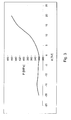
- the profile of the stress P (in MPa) at the edges of the membrane is shown in Fig. 3 as a function of the position of the top surface 9 of the membrane (z) (in relative units with respect to the membrane thickness t of an unsupported portion of a membrane with a substantially uniform thickness) in respect to the overall device surface, which is generally determined by the average position of the upper surface 9 of the membrane at the positions where the membrane 5 is arranged on support structures, here the substrate 1.
- the profile shown in Fig. 3 was calculated using a finite element method, simulating a silicon nitride membrane with a diameter of 30 micron and a thickness t of 1 micron, being deflected at the centre by a pressure difference of 100 kPa.
- a further beneficial effect of having a lowered membrane ( Fig. 2B ) relative to a raised membrane ( Fig. 2A ) and to a membrane of which the top surface 9 is substantially even both over a cavity 6 and over a support structure 1 ( Fig. 1H ), is that the lowered membranes are better protected from the possible damage, when the transducer comes in contact with other objects, in particular solid objects.
- Typical sizes and shapes of electro-acoustic transducer cells fabricated according to the described method are substantially circular structures of several micrometers in diameter, several of which may be arranged to form transducer arrays of various designs.
- the use of known lithography techniques, e.g. for the patterning of the resist layer 2A allow substantially free designing of transducer cells and structures for various purposes, e.g. having different electric and/or acoustic resonance frequencies.
- the amount of sacrificial material 4B in one or more cavities 3 may be varied and/or be structured; this may result in local thickness variations of the membrane material which in turn affect at least its acoustic properties and thus those of the transducer.
- Means for promoting adhesion of the substrate and the membrane material and/or for adapting the crystal structures may be provided for improving at least mechanical properties.
- the present invention allows providing cMUTs with high repeatability since the technology allows relatively easy reproducibility with significantly reduced risks of having uncontrolled changes in device parameters.
Priority Applications (1)
| Application Number | Priority Date | Filing Date | Title |
|---|---|---|---|
| EP08160405A EP2145696A1 (fr) | 2008-07-15 | 2008-07-15 | Transducteur ultrasonique capacitif micro-usiné et procédé de fabrication correspondant |
Applications Claiming Priority (1)
| Application Number | Priority Date | Filing Date | Title |
|---|---|---|---|
| EP08160405A EP2145696A1 (fr) | 2008-07-15 | 2008-07-15 | Transducteur ultrasonique capacitif micro-usiné et procédé de fabrication correspondant |
Publications (1)
| Publication Number | Publication Date |
|---|---|
| EP2145696A1 true EP2145696A1 (fr) | 2010-01-20 |
Family
ID=40070950
Family Applications (1)
| Application Number | Title | Priority Date | Filing Date |
|---|---|---|---|
| EP08160405A Withdrawn EP2145696A1 (fr) | 2008-07-15 | 2008-07-15 | Transducteur ultrasonique capacitif micro-usiné et procédé de fabrication correspondant |
Country Status (1)
| Country | Link |
|---|---|
| EP (1) | EP2145696A1 (fr) |
Cited By (5)
| Publication number | Priority date | Publication date | Assignee | Title |
|---|---|---|---|---|
| CN103906579A (zh) * | 2011-10-28 | 2014-07-02 | 皇家飞利浦有限公司 | 具有塞子的预塌陷电容式微加工换能器单元 |
| CN103917304A (zh) * | 2011-10-28 | 2014-07-09 | 皇家飞利浦有限公司 | 具有应力层的预塌陷电容式微加工换能器单元 |
| CN103958079A (zh) * | 2011-11-17 | 2014-07-30 | 皇家飞利浦有限公司 | 具有环形塌陷区域的预塌陷电容式微机械换能器元件 |
| EP2815700A4 (fr) * | 2012-02-14 | 2015-11-04 | Hitachi Aloka Medical Ltd | Sonde ultrasonore et équipement ultrasonore l'utilisant |
| CN107872760A (zh) * | 2016-09-26 | 2018-04-03 | 思睿逻辑国际半导体有限公司 | Mems设备和方法 |
Citations (8)
| Publication number | Priority date | Publication date | Assignee | Title |
|---|---|---|---|---|
| US5619476A (en) | 1994-10-21 | 1997-04-08 | The Board Of Trustees Of The Leland Stanford Jr. Univ. | Electrostatic ultrasonic transducer |
| US5650572A (en) | 1993-10-25 | 1997-07-22 | Siemens Aktiengesellschaft | Device for ultrasonic flow measurement |
| US5801069A (en) | 1995-09-11 | 1998-09-01 | Mitsubishi Denki Kabushiki Kaisha | Method of fabricating thin film piezoelectric device |
| US5894452A (en) | 1994-10-21 | 1999-04-13 | The Board Of Trustees Of The Leland Stanford Junior University | Microfabricated ultrasonic immersion transducer |
| US20040085858A1 (en) | 2002-08-08 | 2004-05-06 | Khuri-Yakub Butrus T. | Micromachined ultrasonic transducers and method of fabrication |
| US7074634B2 (en) | 2001-05-09 | 2006-07-11 | Consiglio Nazionale Delle Ricerche | Surface micromachining process for manufacturing electro-acoustic transducers, particularly ultrasonic transducers, obtained transducers and intermediate products |
| EP1722595A1 (fr) | 2004-03-05 | 2006-11-15 | Matsushita Electric Industrial Co., Ltd. | Microphone a electret |
| FR2897051A1 (fr) | 2006-02-09 | 2007-08-10 | Gen Electric | Transducteur a ultrasons micro-usine capacitif et procede pour sa fabrication |
-
2008
- 2008-07-15 EP EP08160405A patent/EP2145696A1/fr not_active Withdrawn
Patent Citations (10)
| Publication number | Priority date | Publication date | Assignee | Title |
|---|---|---|---|---|
| US5650572A (en) | 1993-10-25 | 1997-07-22 | Siemens Aktiengesellschaft | Device for ultrasonic flow measurement |
| US5619476A (en) | 1994-10-21 | 1997-04-08 | The Board Of Trustees Of The Leland Stanford Jr. Univ. | Electrostatic ultrasonic transducer |
| US5870351A (en) | 1994-10-21 | 1999-02-09 | The Board Of Trustees Of The Leland Stanford Junior University | Broadband microfabriated ultrasonic transducer and method of fabrication |
| US5894452A (en) | 1994-10-21 | 1999-04-13 | The Board Of Trustees Of The Leland Stanford Junior University | Microfabricated ultrasonic immersion transducer |
| US6004832A (en) | 1994-10-21 | 1999-12-21 | The Board Of Trustees Of The Leland Stanford Junior University | Method of fabricating an electrostatic ultrasonic transducer |
| US5801069A (en) | 1995-09-11 | 1998-09-01 | Mitsubishi Denki Kabushiki Kaisha | Method of fabricating thin film piezoelectric device |
| US7074634B2 (en) | 2001-05-09 | 2006-07-11 | Consiglio Nazionale Delle Ricerche | Surface micromachining process for manufacturing electro-acoustic transducers, particularly ultrasonic transducers, obtained transducers and intermediate products |
| US20040085858A1 (en) | 2002-08-08 | 2004-05-06 | Khuri-Yakub Butrus T. | Micromachined ultrasonic transducers and method of fabrication |
| EP1722595A1 (fr) | 2004-03-05 | 2006-11-15 | Matsushita Electric Industrial Co., Ltd. | Microphone a electret |
| FR2897051A1 (fr) | 2006-02-09 | 2007-08-10 | Gen Electric | Transducteur a ultrasons micro-usine capacitif et procede pour sa fabrication |
Non-Patent Citations (1)
| Title |
|---|
| CALIANO ET AL: "A silicon microfabricated electrostatic transducer: 1 MHz transmission in air and in water", MICROELECTRONIC ENGINEERING, ELSEVIER PUBLISHERS BV., AMSTERDAM, NL, vol. 53, no. 1-4, 1 June 2000 (2000-06-01), pages 573 - 576, XP022553248, ISSN: 0167-9317 * |
Cited By (13)
| Publication number | Priority date | Publication date | Assignee | Title |
|---|---|---|---|---|
| CN103906579B (zh) * | 2011-10-28 | 2016-08-24 | 皇家飞利浦有限公司 | 一种预塌陷电容式微加工换能器单元及其制造方法 |
| CN103917304A (zh) * | 2011-10-28 | 2014-07-09 | 皇家飞利浦有限公司 | 具有应力层的预塌陷电容式微加工换能器单元 |
| CN103906579A (zh) * | 2011-10-28 | 2014-07-02 | 皇家飞利浦有限公司 | 具有塞子的预塌陷电容式微加工换能器单元 |
| CN103917304B (zh) * | 2011-10-28 | 2016-08-17 | 皇家飞利浦有限公司 | 具有应力层的预塌陷电容式微加工换能器单元 |
| CN103958079A (zh) * | 2011-11-17 | 2014-07-30 | 皇家飞利浦有限公司 | 具有环形塌陷区域的预塌陷电容式微机械换能器元件 |
| CN103958079B (zh) * | 2011-11-17 | 2016-08-24 | 皇家飞利浦有限公司 | 具有环形塌陷区域的预塌陷电容式微机械换能器元件 |
| EP2815700A4 (fr) * | 2012-02-14 | 2015-11-04 | Hitachi Aloka Medical Ltd | Sonde ultrasonore et équipement ultrasonore l'utilisant |
| US9846145B2 (en) | 2012-02-14 | 2017-12-19 | Hitachi, Ltd. | Ultrasound probe and ultrasound equipment using same |
| CN107872760A (zh) * | 2016-09-26 | 2018-04-03 | 思睿逻辑国际半导体有限公司 | Mems设备和方法 |
| GB2554470A (en) * | 2016-09-26 | 2018-04-04 | Cirrus Logic Int Semiconductor Ltd | MEMS device and process |
| TWI658986B (zh) * | 2016-09-26 | 2019-05-11 | 席瑞斯邏輯國際半導體有限公司 | Mems裝置與製程 |
| US10477322B2 (en) | 2016-09-26 | 2019-11-12 | Cirrus Logic, Inc. | MEMS device and process |
| CN107872760B (zh) * | 2016-09-26 | 2020-06-23 | 思睿逻辑国际半导体有限公司 | Mems设备 |
Similar Documents
| Publication | Publication Date | Title |
|---|---|---|
| EP3233311B1 (fr) | Transducteurs ultrasoniques micro-usinés piézoélectriques à sensibilité réduite à la contrainte et procédés de fabrication | |
| KR101787187B1 (ko) | 마이크로폰용 시스템 및 방법 | |
| EP2535310B1 (fr) | Dispositifs de type mems à membrane et leurs méthodes de production | |
| EP2692153B1 (fr) | Transducteur acoustique doté d'une géométrie régulant les espaces et procédé de fabrication d'un transducteur acoustique | |
| US6958255B2 (en) | Micromachined ultrasonic transducers and method of fabrication | |
| JP5921079B2 (ja) | 電気機械変換装置及びその作製方法 | |
| EP2771132B1 (fr) | Cellule de transducteur micro-usinée capacitive pré-aplatie dotée d'une couche de contrainte | |
| KR101338856B1 (ko) | 음향 센서 및 그 제조방법 | |
| EP2747904B1 (fr) | Cellule de transducteur micro-usinée capacitive préaffaissée comportant un bouchon | |
| EP2145696A1 (fr) | Transducteur ultrasonique capacitif micro-usiné et procédé de fabrication correspondant | |
| CN112033526B (zh) | 振动传感器及其制造方法 | |
| US10109536B2 (en) | System and method for a microfabricated fracture test structure | |
| JP2012529207A (ja) | マイクロメカニカルマイクロフォン構造体を有する素子、および、マイクロメカニカルマイクロフォン構造体を有する素子の製造方法 | |
| JP5129456B2 (ja) | 梁部を備えた構造体の製造方法およびmemsデバイス | |
| JP6151541B2 (ja) | Mems素子およびその製造方法 | |
| US20130305519A1 (en) | Method Of Manufacturing A Probe Comprising A Cantilever With A Conduit | |
| JP2016022544A (ja) | Mems素子 | |
| JP6659027B2 (ja) | Mems素子およびその製造方法 | |
| CN113747328A (zh) | 微机电结构及其制造方法、晶圆、麦克风和终端 | |
| CN110963458B (zh) | 一种在基板中形成微细结构的方法及微细结构 | |
| CN108540910B (zh) | 麦克风及其制作方法 | |
| JP2018110282A (ja) | 静電容量型トランスデューサ、及びその製造方法 | |
| JP4830545B2 (ja) | 細胞電気生理センサの製造方法 | |
| KR20110029809A (ko) | 초음파 트랜스듀서 및 그 제조 방법 | |
| KR101280349B1 (ko) | Mems 공진기 및 그 제조방법 |
Legal Events
| Date | Code | Title | Description |
|---|---|---|---|
| PUAI | Public reference made under article 153(3) epc to a published international application that has entered the european phase |
Free format text: ORIGINAL CODE: 0009012 |
|
| AK | Designated contracting states |
Kind code of ref document: A1 Designated state(s): AT BE BG CH CY CZ DE DK EE ES FI FR GB GR HR HU IE IS IT LI LT LU LV MC MT NL NO PL PT RO SE SI SK TR |
|
| AX | Request for extension of the european patent |
Extension state: AL BA MK RS |
|
| AKY | No designation fees paid | ||
| REG | Reference to a national code |
Ref country code: DE Ref legal event code: 8566 |
|
| 17P | Request for examination filed |
Effective date: 20101029 |
|
| RBV | Designated contracting states (corrected) |
Designated state(s): AT BE BG CH CY CZ LI |
|
| RBV | Designated contracting states (corrected) |
Designated state(s): AT BE BG CH CY CZ DE DK EE ES FI FR GB GR HR HU IE IS IT LI LT LU LV MC MT NL NO PL PT RO SE SI SK TR |
|
| RBV | Designated contracting states (corrected) |
Designated state(s): AT BE BG CH CY CZ DE DK EE ES FI FR GB GR HR HU IE IS IT LI LT LU LV MC MT NL NO PL PT RO SE SI SK TR |
|
| 17Q | First examination report despatched |
Effective date: 20140611 |
|
| STAA | Information on the status of an ep patent application or granted ep patent |
Free format text: STATUS: THE APPLICATION IS DEEMED TO BE WITHDRAWN |
|
| 18D | Application deemed to be withdrawn |
Effective date: 20151008 |