EP2144113B1 - Optische Vorrichtung, die einen photonischen Kristall auf GaInP-Basis ohne Zwei-Photonen-Absorption umfasst - Google Patents
Optische Vorrichtung, die einen photonischen Kristall auf GaInP-Basis ohne Zwei-Photonen-Absorption umfasst Download PDFInfo
- Publication number
- EP2144113B1 EP2144113B1 EP09164893.1A EP09164893A EP2144113B1 EP 2144113 B1 EP2144113 B1 EP 2144113B1 EP 09164893 A EP09164893 A EP 09164893A EP 2144113 B1 EP2144113 B1 EP 2144113B1
- Authority
- EP
- European Patent Office
- Prior art keywords
- optical
- signal
- optical device
- guide
- layer
- Prior art date
- Legal status (The legal status is an assumption and is not a legal conclusion. Google has not performed a legal analysis and makes no representation as to the accuracy of the status listed.)
- Not-in-force
Links
Images


Classifications
-
- G—PHYSICS
- G02—OPTICS
- G02F—OPTICAL DEVICES OR ARRANGEMENTS FOR THE CONTROL OF LIGHT BY MODIFICATION OF THE OPTICAL PROPERTIES OF THE MEDIA OF THE ELEMENTS INVOLVED THEREIN; NON-LINEAR OPTICS; FREQUENCY-CHANGING OF LIGHT; OPTICAL LOGIC ELEMENTS; OPTICAL ANALOGUE/DIGITAL CONVERTERS
- G02F1/00—Devices or arrangements for the control of the intensity, colour, phase, polarisation or direction of light arriving from an independent light source, e.g. switching, gating or modulating; Non-linear optics
- G02F1/35—Non-linear optics
- G02F1/355—Non-linear optics characterised by the materials used
- G02F1/3556—Semiconductor materials, e.g. quantum wells
-
- B—PERFORMING OPERATIONS; TRANSPORTING
- B82—NANOTECHNOLOGY
- B82Y—SPECIFIC USES OR APPLICATIONS OF NANOSTRUCTURES; MEASUREMENT OR ANALYSIS OF NANOSTRUCTURES; MANUFACTURE OR TREATMENT OF NANOSTRUCTURES
- B82Y20/00—Nanooptics, e.g. quantum optics or photonic crystals
-
- G—PHYSICS
- G02—OPTICS
- G02F—OPTICAL DEVICES OR ARRANGEMENTS FOR THE CONTROL OF LIGHT BY MODIFICATION OF THE OPTICAL PROPERTIES OF THE MEDIA OF THE ELEMENTS INVOLVED THEREIN; NON-LINEAR OPTICS; FREQUENCY-CHANGING OF LIGHT; OPTICAL LOGIC ELEMENTS; OPTICAL ANALOGUE/DIGITAL CONVERTERS
- G02F1/00—Devices or arrangements for the control of the intensity, colour, phase, polarisation or direction of light arriving from an independent light source, e.g. switching, gating or modulating; Non-linear optics
- G02F1/35—Non-linear optics
- G02F1/3511—Self-focusing or self-trapping of light; Light-induced birefringence; Induced optical Kerr-effect
-
- G—PHYSICS
- G02—OPTICS
- G02F—OPTICAL DEVICES OR ARRANGEMENTS FOR THE CONTROL OF LIGHT BY MODIFICATION OF THE OPTICAL PROPERTIES OF THE MEDIA OF THE ELEMENTS INVOLVED THEREIN; NON-LINEAR OPTICS; FREQUENCY-CHANGING OF LIGHT; OPTICAL LOGIC ELEMENTS; OPTICAL ANALOGUE/DIGITAL CONVERTERS
- G02F1/00—Devices or arrangements for the control of the intensity, colour, phase, polarisation or direction of light arriving from an independent light source, e.g. switching, gating or modulating; Non-linear optics
- G02F1/35—Non-linear optics
- G02F1/3515—All-optical modulation, gating, switching, e.g. control of a light beam by another light beam
-
- G—PHYSICS
- G02—OPTICS
- G02F—OPTICAL DEVICES OR ARRANGEMENTS FOR THE CONTROL OF LIGHT BY MODIFICATION OF THE OPTICAL PROPERTIES OF THE MEDIA OF THE ELEMENTS INVOLVED THEREIN; NON-LINEAR OPTICS; FREQUENCY-CHANGING OF LIGHT; OPTICAL LOGIC ELEMENTS; OPTICAL ANALOGUE/DIGITAL CONVERTERS
- G02F1/00—Devices or arrangements for the control of the intensity, colour, phase, polarisation or direction of light arriving from an independent light source, e.g. switching, gating or modulating; Non-linear optics
- G02F1/35—Non-linear optics
- G02F1/3515—All-optical modulation, gating, switching, e.g. control of a light beam by another light beam
- G02F1/3521—All-optical modulation, gating, switching, e.g. control of a light beam by another light beam using a directional coupler
-
- G—PHYSICS
- G02—OPTICS
- G02F—OPTICAL DEVICES OR ARRANGEMENTS FOR THE CONTROL OF LIGHT BY MODIFICATION OF THE OPTICAL PROPERTIES OF THE MEDIA OF THE ELEMENTS INVOLVED THEREIN; NON-LINEAR OPTICS; FREQUENCY-CHANGING OF LIGHT; OPTICAL LOGIC ELEMENTS; OPTICAL ANALOGUE/DIGITAL CONVERTERS
- G02F2202/00—Materials and properties
- G02F2202/32—Photonic crystals
-
- G—PHYSICS
- G02—OPTICS
- G02F—OPTICAL DEVICES OR ARRANGEMENTS FOR THE CONTROL OF LIGHT BY MODIFICATION OF THE OPTICAL PROPERTIES OF THE MEDIA OF THE ELEMENTS INVOLVED THEREIN; NON-LINEAR OPTICS; FREQUENCY-CHANGING OF LIGHT; OPTICAL LOGIC ELEMENTS; OPTICAL ANALOGUE/DIGITAL CONVERTERS
- G02F2203/00—Function characteristic
- G02F2203/15—Function characteristic involving resonance effects, e.g. resonantly enhanced interaction
-
- G—PHYSICS
- G02—OPTICS
- G02F—OPTICAL DEVICES OR ARRANGEMENTS FOR THE CONTROL OF LIGHT BY MODIFICATION OF THE OPTICAL PROPERTIES OF THE MEDIA OF THE ELEMENTS INVOLVED THEREIN; NON-LINEAR OPTICS; FREQUENCY-CHANGING OF LIGHT; OPTICAL LOGIC ELEMENTS; OPTICAL ANALOGUE/DIGITAL CONVERTERS
- G02F2203/00—Function characteristic
- G02F2203/58—Multi-wavelength, e.g. operation of the device at a plurality of wavelengths
- G02F2203/585—Add/drop devices
Definitions
- the field of the invention is that of optical devices based on photonic crystal circuits known to provide original functions in the field of photonics, in particular the all-optical processing of the signal and in particular the sampling of the signal.
- the specificity of this technology is the extreme compactness of the realized structures.
- micro-fabrication e-beam manufacturing, new engraving techniques, etc.
- miniaturized optical components whose properties are remarkable (micro modulators, micro-sensors, nanolasers , etc ...) paving the way for a next phase in which these components will be integrated to achieve a complex optical function.
- the interest of the integration is not so much in improving the performances of a component (for example a modulator or a laser) but rather in the perspective of reducing the bulk, the weight, the consumption and the complexity of the assembly phase of the discrete components when one wants to realize a complex optical function.
- a component for example a modulator or a laser
- Examples of complex optical function may typically be the all-optical routing of information packets or a sampling operation.
- This type of application is based on a key function: a high-speed optical "gate” that opens at a precise time to allow the capture of the header of the packages. Since the rates in question are currently of the order of 10 - 160 Gb / s, these "gates” must switch in less than 10 picoseconds, or even 1 picosecond. These speeds are accessible by exploiting the non-linear optical response.
- the problem in which the present invention thus falls is to have a non-linear response of the Kerr type (refractive index varying with the optical power) without this being accompanied by a 2-photon absorption, followed by a generation of carriers and source of problem.
- materials such as silicon are not suitable for ultra-fast switching applications (area of a few picoseconds).
- a solution presented in literature consists in using direct band semiconductors (for example GaAs and its alumium-based ternary derivatives), the aim being to fix the energy of the forbidden band at a value greater than twice the photon energy involved in the nonlinear process.
- direct band semiconductors for example GaAs and its alumium-based ternary derivatives
- the material of choice is AlGaAs with a molar fraction of aluminum of at least 18%. This material has a strong Kerr-type response and a low 2-photon absorption.
- Photonic crystal technology is well suited to non-linear switching because it allows unprecedented light confinement compared to other optical structures. Recently, a Japanese group ( H. Oda et al., APPLIED PHYSICS LETTERS 90, 231102 (2007) )) has succeeded in producing photonic crystal structures in AlGaAs and shows the Kerr effect.
- the alloy based on Al, Ga, As is a material that is not stable when exposed to oxygen, this phenomenon being amplified by the nanostructuring of the material. This becomes even more serious as the aluminum fraction increases and thus generates a low resistance to the optical flow due to surface defects generated by oxidation.
- the present invention proposes to use a new type of semiconductor material in which it is possible to produce photonic crystal structures, having excellent properties in terms of non-linearity of the third order and exhibiting no phenomenon. of two-photon absorption in the operating wavelength band of the integrating optical device.
- the present invention relates to an optical device operating as an optical gate in a wavelength range centered on a reference wavelength ( ⁇ 0 ) and providing an optical output signal from the injection of a first optical signal
- the optical device comprising a photonic crystal structure comprising a semiconductor substrate and at least one layer of semiconductor material having at least locally a set of periodic patterns corresponding to said photonic crystal structure arranged to form a cavity resonant optics at a wavelength in the operating wavelength range of said device, said semiconductor layer material being an alloy of Gallium, Indium and Phosphorus having no two-photon absorption for photons having a wavelength in the operating wavelength range of said device.
- the device comprises a set of optical cavities for reinforcing the optical output signal.
- the device comprises in said semiconductor layer a first guide and at least one optical cavity coupled to said first guide, at least a first optical signal comprising a set of carrier frequencies and being introduced at said first guide, coupled to the cavity, said cavity providing a filter function and having a resonant frequency such that said frequency makes it possible to extract from said cavity an optical signal at said frequency.
- a first optical signal carrying information is introduced into said guide in a first direction of propagation, a second optical control signal comprising a train of implusions and being introduced into said guide in a second direction propagating opposite said first direction so as to select information contained in said first optical signal.
- the device comprises a second guide coupled to the optical cavity, a first information-carrying optical signal comprising a set of carrier frequencies and being introduced into said first guide, a second optical control signal comprising a pulse train and being introduced into the second guide so as to select information contained in said first optical signal.
- the device comprises a photodetector coupled to said second guide at the end opposite to that by which the control signal is introduced, to recover the optical output signal.
- the first and second guides comprise photonic crystal filters and make it possible to block the control signal
- the device comprises a series of cavities or set of cavities and a series of second guides for addressing a series of control signals.
- the device comprises a series of photodetectors for recovering a series of output signals from the injection of an input optical signal.
- the device comprises a set of optical cavities, making it possible to enhance the interaction of the output optical signal.
- the sacrificial layer is locally disengaged under the layer of semiconductor material comprising the periodic structure.
- the layer of semiconductor material locally comprises a lack of periodic patterns so as to create one or more waveguides, one or more cavities.
- the periodic patterns are holes.
- the present invention provides an optical device incorporating a photonic crystal structure developed in a new type of semiconductor material, in this case a GaInP alloy (in GaAs mesh order) and preferably corresponding to the following chemical formula: Ga 0 , 51 In 0.49 P.
- a new type of semiconductor material in this case a GaInP alloy (in GaAs mesh order) and preferably corresponding to the following chemical formula: Ga 0 , 51 In 0.49 P.
- this material has the same non-linear properties as AlGaAs with a high Al content, while being perfectly stable and resistant to strong optical fluxes.
- the band-gap, the energy gap between the valence band and the GaInP conduction band (precisely Ga 0.51 In 0.49 P), a direct band semiconductor, is about 1.9 eV, negligible two-photon absorption, or even zero, for optical signals in the Telecom band (0.8eV ⁇ 1.9eV / 2).
- figure 2 shows the evolution of the transmission of a photonic crystal structure with a GaAs-type semiconductor material and a GaInP-type semiconductor material according to the invention.
- the transmission is more precisely illustrated by the output power Pout from an input power Pin of a guide made in the structure, this power being expressed in micro watts.
- the two-photon absorption is reflected by a threshold effect of the output power while the GaInP does not exhibit an aborption problem resulting in a saturation effect.
- the Applicant has also experimentally shown properties obtained from photonic crystal waveguides produced within a photonic crystal structure on GaInP.
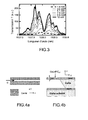
- the figure 3 illustrates in this regard, the spectrum of the transmitted pulse, which shows a strong spectral broadening, proving a self-phase modulation and a hollow in the center of the diagram associated with a non-linear phase change of the order of ⁇ attesting non-linear properties of the material., as described in the article: H. Oda et al., APPLIED PHYSICS LETTERS 90, 231102 (2007) ).
- optical devices comprising a membrane structure in which photonic crystals are produced comprising one or more micro-cavities and one or more waveguides, and in particular examples of optical devices enabling to perform optical switching functions.
- photonic crystals are structures whose dielectric index varies periodically at the wavelength scale over one or more directions of space. Compared to the three-dimensional crystalline structures, it has been shown that a two-dimensional structure could be particularly interesting. In this case, crystals are produced in a thin semiconducting guiding layer, which allows better control and easier technology of compatible production of conventional microelectronics technologies. A very thin layer is thus isolated, thus constituting a membrane that can typically have a thickness h of the order of 150 nanometers to 300 nanometers for applications targeting the spectral range between about 1 micron and 1.6 microns. By a simple scale law, this thickness is adjusted to extend the application to other spectral domains, typically this thickness can be between 0.1 and 0.3 times the wavelength.
- Such a cavity can then provide a filter function with resonance modes or constitute a laser cavity emitting in a plane perpendicular to the plane of the membrane.
- the figure 4a illustrates a top view of a guide G and a cavity Ca made by absence of patterns within a photonic crystal structure Cph developed in a thin layer of GaInP.
- the figure 4b illustrates a sectional view of this thin layer in which one is brought to achieve the various desired functions: resonant cavity, guide, filters, ....
- barrier layer is optional.
- the set of functions can be developed by local etching of the GaInP layer.
- the membrane is released by wet etching of the GaAs sacrificial layer with etching stop on the lower GaInP layer.
- FIGS. 5a and 5b illustrate photographs of photonic crystal structure used in an optical device of the invention and comprising in particular at least one guide G and a cavity Cph, coupled together.
- a carrier wave signal is introduced at one end of the guide.
- the cavity being coupled to the guide and thus powered by the carrier wave signal allows to filter only the frequencies corresponding to the resonant frequencies of the cavity. Following an optical control pulse, this frequency moves and the door opens or closes according to the frequency of the optical carrier of the signal relative to that of the cavity.
- a variant of this structure is an "in line” type configuration, such that the structure transmits to the resonance.
- Another variant consists in the use of several cavities to reinforce the ratio of the signal between the "open” and “closed” states.
- the frequency of the optical cavity may be different from that of the signal, to avoid crosstalk.
- the cavity is designed to have two resonance frequencies.
- One of the major interests of the present invention is to be able to integrate all the functions necessary for the operation of the device within the GaInP layer.
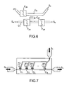
- the figure 6 illustrates in this respect a variant comprising two guides made by breaking periodicity.
- a first input signal Se is introduced into a first guide G 1 and is coupled with the cavity Cph (alternatively, it could be coupled with a set of cavities).
- a control signal S C is in parallel introduced at a second waveguide G 2 , this second waveguide also serves to recover the signal at the output of coupling with the photonic cavity, by a photodetector PD.
- the Fph photonic crystal filter functions are band-pass filters designed to block the control signal and can also be drawn at the frequency break. to avoid unwanted signal feedback that may interfere with useful signals.
- the figure 7 illustrates another variant of optical device of the invention, comprising a series of photonic cavities, a series of photodetectors, a series of second guides, these different components being coupled with an optical signal carrying information packets that should be select with different control signals introduced in the series of second guides.
- optical ports C 1 , C 2 ,..., CN based on photonic crystals make it possible to couple input signals Se and control signals Sc to guides arranged so as to produce an interferometer architecture with a signal. Ss optical output.
- the guides are made within membrane-type photonic crystals, by modification of the periodic structure, typically performed by absence of patterns.
- the device also comprises photodetectors PD1, PD2,..., PDN.
- a series of photodetectors is coupled to the series of second guides, the second guides being bent as shown in FIG. figure 6 .
- the overall size of such a device can be extremely compact, the length of the device illustrated in FIG. figure 7 may be of the order of a few millimeters.
- An alternative to this variant is a device whose series of cavities comprises a set of cavities and no longer a single cavity.
Landscapes
- Physics & Mathematics (AREA)
- Nonlinear Science (AREA)
- Optics & Photonics (AREA)
- General Physics & Mathematics (AREA)
- Chemical & Material Sciences (AREA)
- Engineering & Computer Science (AREA)
- Nanotechnology (AREA)
- Life Sciences & Earth Sciences (AREA)
- Biophysics (AREA)
- Crystallography & Structural Chemistry (AREA)
- Optical Integrated Circuits (AREA)
- Optical Modulation, Optical Deflection, Nonlinear Optics, Optical Demodulation, Optical Logic Elements (AREA)
Claims (14)
- Optische Vorrichtung, die als optische Pforte in einem auf eine Referenzwellenlänge λ0 zentrierten Wellenlängenbereich funktioniert und ab der Einleitung eines ersten optischen Signals ein optisches Ausgangssignal liefert, wobei die optische Vorrichtung eine photonische Kristallstruktur umfasst, die ein Halbleitersubstrat und mindestens eine Halbleitermaterialschicht aufweist, die mindestens lokal eine Gruppe periodischer Motive aufweist, die der photonischen Kristallstruktur entsprechen, die derart angeordnet sind, dass eine optische Resonanzkavität mit einer Wellenlänge im Funktionswellenlängenbereich der Vorrichtung gebildet wird, wobei die Vorrichtung dadurch gekennzeichnet ist, dass das Material der Halbleiterschicht eine Legierung aus Gallium, Indium und Phosphor ist, das für Photonen mit einer Wellenlänge im Funktionswellenlängenbereich der Vorrichtung keine 2-Photonen-Absorption aufweist.
- Optische Vorrichtung nach Anspruch 1, dadurch gekennzeichnet, dass sie eine Gruppe optischer Kavitäten aufweist, die erlauben, das optische Ausgangssignal zu verstärken und die Bandbreite zu erweitern.
- Optische Vorrichtung nach einem der Ansprüche 1 oder 2, dadurch gekennzeichnet, dass sie in der Halbleiterschicht eine erste Führung umfasst, wobei die optische Kavität derart an die erste Führung gekoppelt ist, dass das erste optische Signal, das eine Gruppe von Trägerfrequenzen aufweist, auf Ebene der ersten, an die Kavität gekoppelten Führung einleitbar ist und eine derartige Resonanzfrequenz hat, dass die Frequenz erlaubt, aus der Kavität ein optisches Signal in der Frequenz zu extrahieren.
- Verwendung einer optischen Vorrichtung nach Anspruch 1,die von zwei optischen Signalen adressiert ist, dadurch gekennzeichnet, dass das erste optische Signal als Informationsträger in die Führung gemäß einer ersten Ausbreitungsrichtung eingeleitet wird, wobei ein zweites optisches Steuersignal eine Impulsfolge aufweist und in die Führung gemäß einer zweiten Ausbreitungsrichtung entgegengesetzt zu der ersten Richtung derart eingeleitet wird, dass in dem ersten optischen Signal enthaltene Informationen auswählbar sind.
- Optische Vorrichtung nach Anspruch 1, dadurch gekennzeichnet, dass sie eine zweite Führung umfasst, die an die optische Kavität derart gekoppelt ist, dass das erste optische Signal als Informationsträger, die eine Gruppe von Trägerfrequenzen aufweist, in die erste Führung einleitbar ist und dass ein zweites optisches Steuersignal, das eine Impulsfolge aufweist, in die zweite Führung derart einleitbar ist, dass in dem ersten optischen Signal enthaltene Informationen auswählbar sind.
- Optische Vorrichtung nach Anspruch 5, dadurch gekennzeichnet, dass sie einen an die zweite Führung an dem Ende, das dem gegenüberliegt, durch das das Steuersignal eingeleitet wird, gekoppelten Fotodetektor umfasst, um das optische Ausgangssignal zurückzugewinnen.
- Optische Vorrichtung nach einem der Ansprüche 5 oder 6, dadurch gekennzeichnet, dass die erste und zweite Führung Bandfilter-Photonenkristallfilter aufweisen.
- Optische Vorrichtung nach einem der Ansprüche 5 oder 6, dadurch gekennzeichnet, dass sie eine Reihe von Kavitäten oder Gruppen von Kavitäten und eine Reihe zweiter Führungen umfasst, die erlauben, eine Reihe von Steuersignalen zu adressieren.
- Optische Vorrichtung nach Anspruch 8, dadurch gekennzeichnet, dass sie eine Reihe von Fotodetektoren umfasst, die erlauben, aus einem optischen Eingangssignal eine Reihe von Ausgangsignalen zurückzugewinnen.
- Optische Vorrichtung nach einem der Ansprüche 1 bis 3 und 5 bis 9, dadurch gekennzeichnet, dass sie eine Gruppe optischer Kavitäten aufweist, die erlauben, die Interaktion des optischen Ausgangssignals zu verstärken.
- Optische Vorrichtung nach einem der Ansprüche 1 bis 3 und 5 bis 10, dadurch gekennzeichnet, dass sie auf der Oberfläche eines Substrats aus GaAs die Stapelung folgender Schichten umfasst:- einer GaInP-Schicht,- einer GaAs-Opferschicht,- die Halbleiteimaterialschicht als Ga/In/P- Legierung, die die periodische Struktur aufweist.
- Optische Vorrichtung nach Anspruch 11, dadurch gekennzeichnet, dass die Opferschicht lokal unter der Halbleitermaterialschicht, die die periodische Struktur aufweist, freigelegt ist.
- Optische Vorrichtung nach einem der Ansprüche 1 bis 3 und 5 bis 12, dadurch gekennzeichnet, dass die Halbleitermaterialschicht lokal derart eine Abwesenheit von periodischen Motiven aufweist, dass ein Wellenleiter oder Wellenleiter, eine Kavität oder Kavitäten entstehen.
- Optische Vorrichtung nach einem der Ansprüche 1 bis 3 und 5 bis 13, dadurch gekennzeichnet, dass die periodischen Motive Löcher sind.
Applications Claiming Priority (1)
| Application Number | Priority Date | Filing Date | Title |
|---|---|---|---|
| FR0803991A FR2933786B1 (fr) | 2008-07-11 | 2008-07-11 | Dispositif optique comportant un cristal photonique a base de gainp sans absorption a deux photons |
Publications (2)
| Publication Number | Publication Date |
|---|---|
| EP2144113A1 EP2144113A1 (de) | 2010-01-13 |
| EP2144113B1 true EP2144113B1 (de) | 2015-03-18 |
Family
ID=40276276
Family Applications (1)
| Application Number | Title | Priority Date | Filing Date |
|---|---|---|---|
| EP09164893.1A Not-in-force EP2144113B1 (de) | 2008-07-11 | 2009-07-08 | Optische Vorrichtung, die einen photonischen Kristall auf GaInP-Basis ohne Zwei-Photonen-Absorption umfasst |
Country Status (3)
| Country | Link |
|---|---|
| US (1) | US20100007945A1 (de) |
| EP (1) | EP2144113B1 (de) |
| FR (1) | FR2933786B1 (de) |
Families Citing this family (3)
| Publication number | Priority date | Publication date | Assignee | Title |
|---|---|---|---|---|
| WO2011088367A1 (en) | 2010-01-14 | 2011-07-21 | The Trustees Of Columbia University In The City Of New York | Apparatus and method for generating femtosecond pulses via tempotal solition compression in phtonic crystals |
| KR101063508B1 (ko) * | 2010-03-12 | 2011-09-08 | 인하대학교 산학협력단 | 광잠금 포톤에코 장치 및 방법 |
| CN102654715A (zh) * | 2011-12-27 | 2012-09-05 | 河海大学 | 基于微纳GaAs光学波导的全光调制装置及方法 |
Family Cites Families (12)
| Publication number | Priority date | Publication date | Assignee | Title |
|---|---|---|---|---|
| US6711200B1 (en) * | 1999-09-07 | 2004-03-23 | California Institute Of Technology | Tuneable photonic crystal lasers and a method of fabricating the same |
| US6819845B2 (en) * | 2001-08-02 | 2004-11-16 | Ultradots, Inc. | Optical devices with engineered nonlinear nanocomposite materials |
| FR2834130B1 (fr) * | 2001-12-20 | 2005-02-18 | Thales Sa | Procede d'amelioration des caracteristiques optiques de composants optoelectroniques multicouches |
| JP4569942B2 (ja) * | 2002-09-26 | 2010-10-27 | 三菱電機株式会社 | 光アクティブデバイス |
| FR2855653B1 (fr) * | 2003-05-27 | 2005-10-21 | Thales Sa | Structure amorphe de couplage optique pour detecteur d'ondes electromagnetiques et detecteur associe |
| FR2855654B1 (fr) * | 2003-05-27 | 2006-03-03 | Thales Sa | Detecteur d'ondes electromagnetiques avec surface de couplage optique comprenant des motifs lamellaires |
| FR2863774B1 (fr) * | 2003-12-16 | 2006-03-03 | Thales Sa | Photodetecteur a concentration de champ proche |
| US7483469B2 (en) * | 2004-11-01 | 2009-01-27 | Seiko Epson Corporation | Surface-emitting type semiconductor laser and its manufacturing method, optical module, and light transmission device |
| FR2893184B1 (fr) * | 2005-11-10 | 2007-12-28 | Thales Sa | Structure optique de localisation d'un champ electro-magnetique et dispositif detecteurs ou emetteurs comprenant une telle structure |
| EP2104954B1 (de) * | 2007-01-17 | 2022-03-16 | The Board of Trustees of the University of Illinois | Durch montage auf druckbasis hergestellte optische systeme |
| FR2916093B1 (fr) * | 2007-05-11 | 2009-07-17 | Thales Sa | Lasers semi-conducteurs a contre-reaction repartie monomodes |
| FR2916092B1 (fr) * | 2007-05-11 | 2009-08-07 | Thales Sa | Laser semi-conducteur a contre-reaction repartie forte |
-
2008
- 2008-07-11 FR FR0803991A patent/FR2933786B1/fr active Active
-
2009
- 2009-07-08 EP EP09164893.1A patent/EP2144113B1/de not_active Not-in-force
- 2009-07-09 US US12/499,992 patent/US20100007945A1/en not_active Abandoned
Also Published As
| Publication number | Publication date |
|---|---|
| EP2144113A1 (de) | 2010-01-13 |
| US20100007945A1 (en) | 2010-01-14 |
| FR2933786B1 (fr) | 2010-08-20 |
| FR2933786A1 (fr) | 2010-01-15 |
Similar Documents
| Publication | Publication Date | Title |
|---|---|---|
| US7005669B1 (en) | Quantum dots, nanocomposite materials with quantum dots, devices with quantum dots, and related fabrication methods | |
| Jalali et al. | Silicon photonics | |
| EP0575227B1 (de) | Verfahren und Vorrichtung zur Modulation und Verstärkung von Lichtstrahlen | |
| US6870970B2 (en) | Method of varying optical properties of photonic crystals on fast time scales using energy pulses | |
| JP2002277912A (ja) | 光スイッチ、トランジスタ、コンピュータシステムおよび光信号のスイッチ方法 | |
| EP1162769B1 (de) | Vorrichtung zum Regenerieren optischer Signale | |
| FR2683054A1 (fr) | Modulateur electrooptique integre et procede de fabrication de ce modulateur. | |
| EP0750756A1 (de) | Wellenleiterfrequenzwandler mit hohem wirkungsgrad | |
| WO2001050554A1 (fr) | Structure de reseau par holographie de volume a forte dispersion | |
| EP2144113A1 (de) | Optische Vorrichtung, die einen Photonenkristall auf GaInP-Basis ohne Absorption mit zwei Photonen umfasst | |
| EP1470622B1 (de) | Sättigbares absorberbauteil und verfahren zu dessen herstellung | |
| CA2367708A1 (fr) | Circuit photonique integre comprenant un composant optique resonant et procedes de fabrication de ce circuit | |
| EP0992842B1 (de) | Vorrichtung zum Regenerieren eines Wellenmultiplexsignales mit einem sättigbaren Absorber | |
| EP1089405B1 (de) | Halbleiterlaser mit parametrischer Lichterzeugung | |
| CA2769478A1 (fr) | Dispositifs electro-optiques bases sur la variation d'indice ou d'absorption dans des transitions isb | |
| EP0350110A1 (de) | Integriertes optoelektronisches Halbleitergerät mit einem TE/TM-Modenteiler | |
| EP3599501B1 (de) | Athermischer modulator-umschalter mit zwei übereinander angeordneten ringen | |
| Moss | Novel functions in silicon photonic chips incorporated with graphene oxide thin films | |
| WO2020193786A9 (fr) | Modulateur ultra-rapide de l'amplitude d'un rayonnement laser | |
| FR2713788A1 (fr) | Opérateur optique à hétérostructure à puits quantiques. | |
| Moss | Graphene oxide thin films expand the functionality of silicon photonic chips | |
| Moss | Novel photo-thermal functionality in silicon photonic chips with 2D graphene oxide films | |
| Moss | Optical isolator and power limiter in silicon nanowires with 2D graphene oxide films | |
| Moss | Photo-thermal based novel functions in silicon photonic chips with 2D graphene oxide films | |
| Moss | Novel functionality based on photo-thermal effects in silicon photonic chips with 2D graphene oxide films |
Legal Events
| Date | Code | Title | Description |
|---|---|---|---|
| PUAI | Public reference made under article 153(3) epc to a published international application that has entered the european phase |
Free format text: ORIGINAL CODE: 0009012 |
|
| AK | Designated contracting states |
Kind code of ref document: A1 Designated state(s): AT BE BG CH CY CZ DE DK EE ES FI FR GB GR HR HU IE IS IT LI LT LU LV MC MK MT NL NO PL PT RO SE SI SK SM TR |
|
| 17P | Request for examination filed |
Effective date: 20100507 |
|
| 17Q | First examination report despatched |
Effective date: 20100602 |
|
| GRAP | Despatch of communication of intention to grant a patent |
Free format text: ORIGINAL CODE: EPIDOSNIGR1 |
|
| INTG | Intention to grant announced |
Effective date: 20141119 |
|
| GRAS | Grant fee paid |
Free format text: ORIGINAL CODE: EPIDOSNIGR3 |
|
| GRAA | (expected) grant |
Free format text: ORIGINAL CODE: 0009210 |
|
| AK | Designated contracting states |
Kind code of ref document: B1 Designated state(s): AT BE BG CH CY CZ DE DK EE ES FI FR GB GR HR HU IE IS IT LI LT LU LV MC MK MT NL NO PL PT RO SE SI SK SM TR |
|
| REG | Reference to a national code |
Ref country code: GB Ref legal event code: FG4D Free format text: NOT ENGLISH |
|
| REG | Reference to a national code |
Ref country code: CH Ref legal event code: EP |
|
| REG | Reference to a national code |
Ref country code: IE Ref legal event code: FG4D Free format text: LANGUAGE OF EP DOCUMENT: FRENCH |
|
| REG | Reference to a national code |
Ref country code: AT Ref legal event code: REF Ref document number: 716933 Country of ref document: AT Kind code of ref document: T Effective date: 20150415 |
|
| REG | Reference to a national code |
Ref country code: DE Ref legal event code: R096 Ref document number: 602009030010 Country of ref document: DE Effective date: 20150430 |
|
| REG | Reference to a national code |
Ref country code: NL Ref legal event code: VDEP Effective date: 20150318 |
|
| REG | Reference to a national code |
Ref country code: NL Ref legal event code: VDEP Effective date: 20150318 |
|
| PG25 | Lapsed in a contracting state [announced via postgrant information from national office to epo] |
Ref country code: SE Free format text: LAPSE BECAUSE OF FAILURE TO SUBMIT A TRANSLATION OF THE DESCRIPTION OR TO PAY THE FEE WITHIN THE PRESCRIBED TIME-LIMIT Effective date: 20150318 Ref country code: HR Free format text: LAPSE BECAUSE OF FAILURE TO SUBMIT A TRANSLATION OF THE DESCRIPTION OR TO PAY THE FEE WITHIN THE PRESCRIBED TIME-LIMIT Effective date: 20150318 Ref country code: LT Free format text: LAPSE BECAUSE OF FAILURE TO SUBMIT A TRANSLATION OF THE DESCRIPTION OR TO PAY THE FEE WITHIN THE PRESCRIBED TIME-LIMIT Effective date: 20150318 Ref country code: FI Free format text: LAPSE BECAUSE OF FAILURE TO SUBMIT A TRANSLATION OF THE DESCRIPTION OR TO PAY THE FEE WITHIN THE PRESCRIBED TIME-LIMIT Effective date: 20150318 Ref country code: NO Free format text: LAPSE BECAUSE OF FAILURE TO SUBMIT A TRANSLATION OF THE DESCRIPTION OR TO PAY THE FEE WITHIN THE PRESCRIBED TIME-LIMIT Effective date: 20150618 |
|
| REG | Reference to a national code |
Ref country code: AT Ref legal event code: MK05 Ref document number: 716933 Country of ref document: AT Kind code of ref document: T Effective date: 20150318 |
|
| REG | Reference to a national code |
Ref country code: LT Ref legal event code: MG4D |
|
| PG25 | Lapsed in a contracting state [announced via postgrant information from national office to epo] |
Ref country code: GR Free format text: LAPSE BECAUSE OF FAILURE TO SUBMIT A TRANSLATION OF THE DESCRIPTION OR TO PAY THE FEE WITHIN THE PRESCRIBED TIME-LIMIT Effective date: 20150619 Ref country code: LV Free format text: LAPSE BECAUSE OF FAILURE TO SUBMIT A TRANSLATION OF THE DESCRIPTION OR TO PAY THE FEE WITHIN THE PRESCRIBED TIME-LIMIT Effective date: 20150318 |
|
| PG25 | Lapsed in a contracting state [announced via postgrant information from national office to epo] |
Ref country code: NL Free format text: LAPSE BECAUSE OF FAILURE TO SUBMIT A TRANSLATION OF THE DESCRIPTION OR TO PAY THE FEE WITHIN THE PRESCRIBED TIME-LIMIT Effective date: 20150318 |
|
| PG25 | Lapsed in a contracting state [announced via postgrant information from national office to epo] |
Ref country code: ES Free format text: LAPSE BECAUSE OF FAILURE TO SUBMIT A TRANSLATION OF THE DESCRIPTION OR TO PAY THE FEE WITHIN THE PRESCRIBED TIME-LIMIT Effective date: 20150318 Ref country code: SK Free format text: LAPSE BECAUSE OF FAILURE TO SUBMIT A TRANSLATION OF THE DESCRIPTION OR TO PAY THE FEE WITHIN THE PRESCRIBED TIME-LIMIT Effective date: 20150318 Ref country code: CZ Free format text: LAPSE BECAUSE OF FAILURE TO SUBMIT A TRANSLATION OF THE DESCRIPTION OR TO PAY THE FEE WITHIN THE PRESCRIBED TIME-LIMIT Effective date: 20150318 Ref country code: EE Free format text: LAPSE BECAUSE OF FAILURE TO SUBMIT A TRANSLATION OF THE DESCRIPTION OR TO PAY THE FEE WITHIN THE PRESCRIBED TIME-LIMIT Effective date: 20150318 Ref country code: PT Free format text: LAPSE BECAUSE OF FAILURE TO SUBMIT A TRANSLATION OF THE DESCRIPTION OR TO PAY THE FEE WITHIN THE PRESCRIBED TIME-LIMIT Effective date: 20150720 Ref country code: RO Free format text: LAPSE BECAUSE OF FAILURE TO SUBMIT A TRANSLATION OF THE DESCRIPTION OR TO PAY THE FEE WITHIN THE PRESCRIBED TIME-LIMIT Effective date: 20150318 |
|
| PG25 | Lapsed in a contracting state [announced via postgrant information from national office to epo] |
Ref country code: AT Free format text: LAPSE BECAUSE OF FAILURE TO SUBMIT A TRANSLATION OF THE DESCRIPTION OR TO PAY THE FEE WITHIN THE PRESCRIBED TIME-LIMIT Effective date: 20150318 Ref country code: IS Free format text: LAPSE BECAUSE OF FAILURE TO SUBMIT A TRANSLATION OF THE DESCRIPTION OR TO PAY THE FEE WITHIN THE PRESCRIBED TIME-LIMIT Effective date: 20150718 Ref country code: PL Free format text: LAPSE BECAUSE OF FAILURE TO SUBMIT A TRANSLATION OF THE DESCRIPTION OR TO PAY THE FEE WITHIN THE PRESCRIBED TIME-LIMIT Effective date: 20150318 |
|
| REG | Reference to a national code |
Ref country code: DE Ref legal event code: R097 Ref document number: 602009030010 Country of ref document: DE |
|
| PG25 | Lapsed in a contracting state [announced via postgrant information from national office to epo] |
Ref country code: IT Free format text: LAPSE BECAUSE OF FAILURE TO SUBMIT A TRANSLATION OF THE DESCRIPTION OR TO PAY THE FEE WITHIN THE PRESCRIBED TIME-LIMIT Effective date: 20150318 |
|
| PLBE | No opposition filed within time limit |
Free format text: ORIGINAL CODE: 0009261 |
|
| STAA | Information on the status of an ep patent application or granted ep patent |
Free format text: STATUS: NO OPPOSITION FILED WITHIN TIME LIMIT |
|
| PG25 | Lapsed in a contracting state [announced via postgrant information from national office to epo] |
Ref country code: DK Free format text: LAPSE BECAUSE OF FAILURE TO SUBMIT A TRANSLATION OF THE DESCRIPTION OR TO PAY THE FEE WITHIN THE PRESCRIBED TIME-LIMIT Effective date: 20150318 |
|
| REG | Reference to a national code |
Ref country code: DE Ref legal event code: R119 Ref document number: 602009030010 Country of ref document: DE |
|
| 26N | No opposition filed |
Effective date: 20151221 |
|
| PG25 | Lapsed in a contracting state [announced via postgrant information from national office to epo] |
Ref country code: SI Free format text: LAPSE BECAUSE OF FAILURE TO SUBMIT A TRANSLATION OF THE DESCRIPTION OR TO PAY THE FEE WITHIN THE PRESCRIBED TIME-LIMIT Effective date: 20150318 Ref country code: MC Free format text: LAPSE BECAUSE OF FAILURE TO SUBMIT A TRANSLATION OF THE DESCRIPTION OR TO PAY THE FEE WITHIN THE PRESCRIBED TIME-LIMIT Effective date: 20150318 |
|
| REG | Reference to a national code |
Ref country code: CH Ref legal event code: PL |
|
| GBPC | Gb: european patent ceased through non-payment of renewal fee |
Effective date: 20150708 |
|
| PG25 | Lapsed in a contracting state [announced via postgrant information from national office to epo] |
Ref country code: LU Free format text: LAPSE BECAUSE OF FAILURE TO SUBMIT A TRANSLATION OF THE DESCRIPTION OR TO PAY THE FEE WITHIN THE PRESCRIBED TIME-LIMIT Effective date: 20150708 |
|
| REG | Reference to a national code |
Ref country code: IE Ref legal event code: MM4A |
|
| PG25 | Lapsed in a contracting state [announced via postgrant information from national office to epo] |
Ref country code: CH Free format text: LAPSE BECAUSE OF NON-PAYMENT OF DUE FEES Effective date: 20150731 Ref country code: DE Free format text: LAPSE BECAUSE OF NON-PAYMENT OF DUE FEES Effective date: 20160202 Ref country code: LI Free format text: LAPSE BECAUSE OF NON-PAYMENT OF DUE FEES Effective date: 20150731 Ref country code: GB Free format text: LAPSE BECAUSE OF NON-PAYMENT OF DUE FEES Effective date: 20150708 |
|
| REG | Reference to a national code |
Ref country code: FR Ref legal event code: PLFP Year of fee payment: 8 |
|
| PG25 | Lapsed in a contracting state [announced via postgrant information from national office to epo] |
Ref country code: IE Free format text: LAPSE BECAUSE OF NON-PAYMENT OF DUE FEES Effective date: 20150708 |
|
| PG25 | Lapsed in a contracting state [announced via postgrant information from national office to epo] |
Ref country code: MT Free format text: LAPSE BECAUSE OF FAILURE TO SUBMIT A TRANSLATION OF THE DESCRIPTION OR TO PAY THE FEE WITHIN THE PRESCRIBED TIME-LIMIT Effective date: 20150318 |
|
| PG25 | Lapsed in a contracting state [announced via postgrant information from national office to epo] |
Ref country code: SM Free format text: LAPSE BECAUSE OF FAILURE TO SUBMIT A TRANSLATION OF THE DESCRIPTION OR TO PAY THE FEE WITHIN THE PRESCRIBED TIME-LIMIT Effective date: 20150318 Ref country code: HU Free format text: LAPSE BECAUSE OF FAILURE TO SUBMIT A TRANSLATION OF THE DESCRIPTION OR TO PAY THE FEE WITHIN THE PRESCRIBED TIME-LIMIT; INVALID AB INITIO Effective date: 20090708 Ref country code: BG Free format text: LAPSE BECAUSE OF FAILURE TO SUBMIT A TRANSLATION OF THE DESCRIPTION OR TO PAY THE FEE WITHIN THE PRESCRIBED TIME-LIMIT Effective date: 20150318 |
|
| REG | Reference to a national code |
Ref country code: FR Ref legal event code: PLFP Year of fee payment: 9 |
|
| PG25 | Lapsed in a contracting state [announced via postgrant information from national office to epo] |
Ref country code: CY Free format text: LAPSE BECAUSE OF FAILURE TO SUBMIT A TRANSLATION OF THE DESCRIPTION OR TO PAY THE FEE WITHIN THE PRESCRIBED TIME-LIMIT Effective date: 20150318 |
|
| PG25 | Lapsed in a contracting state [announced via postgrant information from national office to epo] |
Ref country code: BE Free format text: LAPSE BECAUSE OF NON-PAYMENT OF DUE FEES Effective date: 20150731 |
|
| PG25 | Lapsed in a contracting state [announced via postgrant information from national office to epo] |
Ref country code: TR Free format text: LAPSE BECAUSE OF FAILURE TO SUBMIT A TRANSLATION OF THE DESCRIPTION OR TO PAY THE FEE WITHIN THE PRESCRIBED TIME-LIMIT Effective date: 20150318 |
|
| REG | Reference to a national code |
Ref country code: FR Ref legal event code: PLFP Year of fee payment: 10 |
|
| PG25 | Lapsed in a contracting state [announced via postgrant information from national office to epo] |
Ref country code: MK Free format text: LAPSE BECAUSE OF FAILURE TO SUBMIT A TRANSLATION OF THE DESCRIPTION OR TO PAY THE FEE WITHIN THE PRESCRIBED TIME-LIMIT Effective date: 20150318 |
|
| PGFP | Annual fee paid to national office [announced via postgrant information from national office to epo] |
Ref country code: FR Payment date: 20230622 Year of fee payment: 15 |
|
| PG25 | Lapsed in a contracting state [announced via postgrant information from national office to epo] |
Ref country code: FR Free format text: LAPSE BECAUSE OF NON-PAYMENT OF DUE FEES Effective date: 20240731 |