EP2141741A2 - Circuit électronique comprenant un transistor MOS monté en diode à rendement amélioré - Google Patents
Circuit électronique comprenant un transistor MOS monté en diode à rendement amélioré Download PDFInfo
- Publication number
- EP2141741A2 EP2141741A2 EP09164596A EP09164596A EP2141741A2 EP 2141741 A2 EP2141741 A2 EP 2141741A2 EP 09164596 A EP09164596 A EP 09164596A EP 09164596 A EP09164596 A EP 09164596A EP 2141741 A2 EP2141741 A2 EP 2141741A2
- Authority
- EP
- European Patent Office
- Prior art keywords
- transistor
- diode
- power terminal
- source
- mos transistor
- Prior art date
- Legal status (The legal status is an assumption and is not a legal conclusion. Google has not performed a legal analysis and makes no representation as to the accuracy of the status listed.)
- Withdrawn
Links
Images


Classifications
-
- H—ELECTRICITY
- H10—SEMICONDUCTOR DEVICES; ELECTRIC SOLID-STATE DEVICES NOT OTHERWISE PROVIDED FOR
- H10D—INORGANIC ELECTRIC SEMICONDUCTOR DEVICES
- H10D84/00—Integrated devices formed in or on semiconductor substrates that comprise only semiconducting layers, e.g. on Si wafers or on GaAs-on-Si wafers
- H10D84/201—Integrated devices formed in or on semiconductor substrates that comprise only semiconducting layers, e.g. on Si wafers or on GaAs-on-Si wafers characterised by the integration of only components covered by H10D1/00 or H10D8/00, e.g. RLC circuits
- H10D84/204—Integrated devices formed in or on semiconductor substrates that comprise only semiconducting layers, e.g. on Si wafers or on GaAs-on-Si wafers characterised by the integration of only components covered by H10D1/00 or H10D8/00, e.g. RLC circuits of combinations of diodes or capacitors or resistors
- H10D84/212—Integrated devices formed in or on semiconductor substrates that comprise only semiconducting layers, e.g. on Si wafers or on GaAs-on-Si wafers characterised by the integration of only components covered by H10D1/00 or H10D8/00, e.g. RLC circuits of combinations of diodes or capacitors or resistors of only capacitors
- H10D84/217—Integrated devices formed in or on semiconductor substrates that comprise only semiconducting layers, e.g. on Si wafers or on GaAs-on-Si wafers characterised by the integration of only components covered by H10D1/00 or H10D8/00, e.g. RLC circuits of combinations of diodes or capacitors or resistors of only capacitors of only conductor-insulator-semiconductor capacitors
-
- H—ELECTRICITY
- H02—GENERATION; CONVERSION OR DISTRIBUTION OF ELECTRIC POWER
- H02M—APPARATUS FOR CONVERSION BETWEEN AC AND AC, BETWEEN AC AND DC, OR BETWEEN DC AND DC, AND FOR USE WITH MAINS OR SIMILAR POWER SUPPLY SYSTEMS; CONVERSION OF DC OR AC INPUT POWER INTO SURGE OUTPUT POWER; CONTROL OR REGULATION THEREOF
- H02M3/00—Conversion of DC power input into DC power output
- H02M3/02—Conversion of DC power input into DC power output without intermediate conversion into AC
- H02M3/04—Conversion of DC power input into DC power output without intermediate conversion into AC by static converters
- H02M3/06—Conversion of DC power input into DC power output without intermediate conversion into AC by static converters using resistors or capacitors, e.g. potential divider
- H02M3/07—Conversion of DC power input into DC power output without intermediate conversion into AC by static converters using resistors or capacitors, e.g. potential divider using capacitors charged and discharged alternately by semiconductor devices with control electrode, e.g. charge pumps
-
- H—ELECTRICITY
- H10—SEMICONDUCTOR DEVICES; ELECTRIC SOLID-STATE DEVICES NOT OTHERWISE PROVIDED FOR
- H10D—INORGANIC ELECTRIC SEMICONDUCTOR DEVICES
- H10D30/00—Field-effect transistors [FET]
- H10D30/60—Insulated-gate field-effect transistors [IGFET]
- H10D30/721—Insulated-gate field-effect transistors [IGFET] having a gate-to-body connection, i.e. bulk dynamic threshold voltage IGFET
-
- H—ELECTRICITY
- H10—SEMICONDUCTOR DEVICES; ELECTRIC SOLID-STATE DEVICES NOT OTHERWISE PROVIDED FOR
- H10D—INORGANIC ELECTRIC SEMICONDUCTOR DEVICES
- H10D8/00—Diodes
-
- H—ELECTRICITY
- H10—SEMICONDUCTOR DEVICES; ELECTRIC SOLID-STATE DEVICES NOT OTHERWISE PROVIDED FOR
- H10D—INORGANIC ELECTRIC SEMICONDUCTOR DEVICES
- H10D84/00—Integrated devices formed in or on semiconductor substrates that comprise only semiconducting layers, e.g. on Si wafers or on GaAs-on-Si wafers
- H10D84/80—Integrated devices formed in or on semiconductor substrates that comprise only semiconducting layers, e.g. on Si wafers or on GaAs-on-Si wafers characterised by the integration of at least one component covered by groups H10D12/00 or H10D30/00, e.g. integration of IGFETs
- H10D84/811—Combinations of field-effect devices and one or more diodes, capacitors or resistors
Definitions
- the present invention relates to an electronic circuit comprising a MOSFET (metal oxide semiconductor field effect transistor) or diode-mounted MOS transistor, one of whose power terminals receives an oscillating signal, for example of an alternating signal.
- MOSFET metal oxide semiconductor field effect transistor
- diode-mounted MOS transistor one of whose power terminals receives an oscillating signal, for example of an alternating signal.
- the single-wave rectifier circuit consists of a recovery stage, followed by a filtering stage.
- the rectifying stage may comprise a diode which makes it possible to retain, for example, only the positive half-waves of the input signal.
- the filter stage may comprise a capacitor and provide a substantially continuous signal from the positive half cycles.
- the diode is usually replaced by a MOS transistor, mounted diode, that is to say whose gate is connected to the drain.
- MOS transistor mounted diode
- the bulk of the energy losses of the rectifier circuit realized integrally from the transistor when it is passing and depend on the product between the current flowing through the transistor and the drain-source voltage of the transistor.
- the channel current of the transistor varies according to the gate-source voltage, that is to say the drain-source voltage.
- the threshold voltage of the transistor it is necessary that the drain-source voltage remains as low as possible when the transistor is on. It is therefore desirable for the threshold voltage of the transistor to be as low as possible.
- the MOS transistor is formed in and on a layer of semiconductor material polarized by a source of a reference potential, for example ground.
- a source of a reference potential for example ground.
- it is difficult to significantly reduce the threshold voltage of the transistor.
- additional losses are observed because of the leakage current of the MOS transistor in the off state and the conduction of parasitic diodes of the transistor.
- the present invention relates to an electronic circuit comprising a diode-mounted MOS transistor, one of whose power terminals receives an oscillating signal, for example an alternating signal, having reduced losses when the transistor is on.
- the invention aims at reducing the losses due to the leakage current of the transistor when the transistor is off.
- the present invention aims to reduce the losses due to the conduction of parasitic diodes during the evolution of the oscillating signal while the transistor is blocked.
- an embodiment of the present invention provides an integrated circuit having a semiconductor layer; and a MOS transistor comprising first and second power terminals and a substrate isolated from the semiconductor layer, the first power terminal being for receiving an oscillating signal, the gate of the transistor and the substrate being connected to the first power terminal.
- the substrate corresponds to a portion of the semiconductor layer isolated from the remainder of the semiconductor layer by a doped region, the doped region being connected to the second power terminal.
- the doped region is of a first type of conductivity
- the first and second power terminals comprising additional doped regions of the first type of conductivity
- the semiconductor layer being undoped or doped with a second type of conductivity, said portion of the semiconductor layer extending at least between the additional doped regions.
- the circuit comprises a filter connected to the second power terminal.
- the MOS transistor is an N-channel MOS transistor.
- An aspect of the present invention is an electronic circuit comprising an integrated circuit as defined above; and a source of a reference potential connected to the semiconductor layer.
- the electronic circuit further comprises a first capacitor comprising a first armature connected to the first power terminal; a second capacitor comprising a second armature connected to the second power terminal and a third armature connected to the source of the reference potential; and an additional diode-mounted MOS transistor comprising a third power terminal connected to the first power terminal and a fourth power terminal connected to the source of the reference potential.
- the electronic circuit further comprises a first capacitor comprising a first armature connected to the second power terminal and a second armature; a second capacitor comprising a third armature connected to the second armature and a third armature connected to the source of the reference potential; and an additional diode-mounted MOS transistor comprising a third power terminal connected to the first power terminal and a fourth power terminal connected to the source of the reference potential.
- the electronic circuit further comprises a power source; an inductor connecting the power source to the first power terminal; an additional MOS transistor comprising a third power terminal connected to the first power terminal and a fourth power terminal connected to the source of the reference potential; a source of a succession of voltage pulses at the gate of the additional MOS transistor; and a capacitor comprising a first armature connected to the second power terminal and a second armature connected to the source of the reference potential.
- an oscillating signal is a signal that alternately passes from an extreme high value to an extreme low value.
- the extreme high and low values may be of opposite signs.
- the signal is then called alternative. He then successively understands a positive alternation, a negative alternation, a positive alternation, a negative alternation, etc.
- the oscillating signal may be periodic.
- the figure 1 schematically represents a single-phase rectifier circuit with a capacitor filter.
- the circuit 10 comprises two input terminals N 1 and N 2 between which is applied an oscillating voltage V IN , for example an alternating voltage.
- the AC voltage V IN is a sinusoidal voltage.
- the voltage V IN can be provided from a radiofrequency signal picked up by an antenna.
- the AC voltage V IN is a periodic voltage, comprising, for each period, a positive half cycle and a negative half cycle.
- the input terminal N 2 is connected to a source of a reference potential, for example the ground GND.
- the circuit 10 comprises a diode diode whose anode is connected to the input terminal N 1 and whose cathode is connected to a node E.
- a capacitor C is arranged between the node E and a node F connected to the ground GND .
- a resistor R is arranged in parallel across the capacitor C.
- the reference V OUT denotes the voltage between the nodes E and F.
- the function performed by the diode diode of the circuit 10 is performed by a diode-mounted MOS transistor.
- the figure 2 represents an example of a conventional structure of a diode-mounted MOS transistor M formed at a layer 12 of a semiconductor material, for example P-type doped monocrystalline silicon, having an upper surface 13.
- the transistor M is an N-channel transistor.
- the MOS transistor comprises an insulating portion 14, for example made of silicon oxide, covering the layer 12.
- Regions N-type dopants 18, 20 are provided in the layer 12 on either side of the insulating portion 14.
- the regions 18 and 20 extend optionally partially under the insulating portion 14.
- a P-type doped region 22 extends in the layer 12 from the surface 13.
- the region 22 is more heavily doped than the layer 12.
- the insulating portion 14 constitutes the gate insulator of the transistor M and the portion 16 constitutes the gate of the transistor M.
- the region 18 constitutes the source region of the transistor M and the region 20 constitutes the drain region of the transistor M.
- the connections of the elements of the transistor M are made by conductive tracks and vias not shown in detail.
- a terminal G connected to the portion 16, a terminal S connected to the source region 18 and a terminal D connected to the drain region.
- a terminal B is connected to the region 22 and makes it possible to polarize the layer 12.
- gate 16 of transistor M is indifferently referred to as the portion 16 or terminal G
- source of transistor M is region 18 or terminal S
- drain of the transistor M the region 20 or the terminal D.
- the transistor M being diode-mounted, the gate G is connected to the drain D.
- a first parasitic diode Diode BS corresponds to the junction between the layer 12 and the source region 18.
- a second parasitic diode Diode BD corresponds to the junction between the layer 12 and the region of drain 20.
- the figure 3 represents a rectifying circuit 25 similar to the circuit 10 of the figure 1 wherein the function filled by the diode diode is made from the diode-mounted transistor M of the figure 2 .
- the drain D of the transistor M is connected to the input terminal N 1 .
- the source S of the transistor M is connected to the node E.
- the substrate B of the transistor M is biased to ground GND.
- V DS is the voltage between the drain D and the source S of the transistor M
- V GS the voltage between the gate G and the source S of the transistor M
- I N1 is the current at the input terminal N 1 .
- the rectifier circuit 25 is intended to be connected to other circuits at the nodes E and F.
- the losses of the circuit 25 due to the conduction of the transistor M are proportional to the product of the voltage V DS , equal to the voltage V GS , and the current I DS . These losses occur, in steady state, when the voltage V GS is greater than the threshold voltage V t0 .
- the threshold voltage V t0 of the transistor M it is desirable for the threshold voltage V t0 of the transistor M to be as low as possible.
- the relation (1) shows that the threshold voltage V t0 is directly imposed by the value of the voltage V OUT which is generally fixed by the intended application of the rectifier circuit 25. It is therefore difficult to reduce the threshold voltage V t0 .
- the transistor M has a leakage current in the off state, in particular during the negative half-waves of the voltage V IN , which increases the losses of the circuit 25.
- the higher the threshold voltage of a MOS transistor is low the higher the leakage current is important. It is therefore not possible with the circuit 25 to simultaneously reduce the threshold voltage V t0 and the leakage current of the MOS transistor.
- the figure 4 represents the rectifier circuit 25 of the figure 3 in which the parasitic diode diodes BS and diode BD of the transistor M have been represented.
- the parasitic diode Diode BD extends between the terminals N 1 and N 2 , the anode of the diode Diode BD being connected to the input terminal N 2 .
- the parasitic diode Diode BS extends between the nodes E and F, the anode of the diode Diode BS being connected to the node F.
- the diode diode BD diode can become busy. This increases the losses of the circuit 25.
- the input impedance of the circuit 25 is high.
- the input impedance of the circuit 25 drops, which can be detrimental for certain applications. It may therefore be necessary to limit the amplitude of the voltage V IN to prevent the fall of the input impedance of the circuit 25.
- the figure 5 represents the structure of a diode-connected transistor M 'according to an exemplary embodiment of the invention.
- the transistor M ' comprises a substrate isolation structure 30 which delimits a portion 32 of the semiconductor layer 12 around the source and drain regions 18, 20 of the transistor M'.
- the portion 32, electrically isolated from the remainder of the layer 12, is called substrate 32 (in English bulk or body) of the transistor M 'in the following description.
- the doping of the region 32 is chosen to be sufficiently small so that the threshold voltage of the MOS transistor is substantially less than 0.6 V, preferably between 0.1 and 0.3 V.
- the substrate isolation structure 30 comprises a buried N type buried region 34 lying in the layer 12 and extending under the regions 18, 20 and 22.
- the substrate isolation structure 30 further comprises a side wall 36 corresponding to a region of the type N extending from the surface 13 of the layer 12 to the buried region 34 and surrounding the regions 18, 20 and 22.
- a region 38, N-type, more strongly doped than the region 36 extends in the region 36.
- An AC bias terminal of the substrate isolation structure 30 is connected to the region 38.
- a P-type doped region 39 extends in the layer 12 from the surface 13 outside the the substrate isolation structure.
- a terminal W is connected to the region 39 and makes it possible to polarize the remainder of the layer 12. Since the transistor M 'is diode-mounted, the gate G is connected to the In addition, the bias terminal B of the substrate 32 is connected to the drain D and the bias AC terminal of the substrate isolation structure 30 is connected to the source S.
- the polarization terminal W of the layer 12 is connected to the source of the reference potential GND.
- the intrinsic parasitic diodes of the transistor M ' corresponds to the junction between the substrate 32 of the transistor M 'and the source region 18.
- the diode Diode BD corresponds to the junction between the substrate 32 of the transistor M' and the drain region 20.
- the diode W diode corresponds to the junction between the substrate isolation structure 30 and the portion of the layer 12 outside the substrate isolation structure 30.
- the diode ISO diode corresponds to the junction between the substrate 32 of the transistor M 'and the substrate isolation structure 30.
- the figure 6 represents a rectifier circuit 40 similar to the rectifier circuit 25 of the figure 3 in which the transistor M 'is used.
- the diodes Diode ISO and Diode BS extend between the drain D and the node E, the anodes of the diodes Diode ISO and Diode BS being connected to the drain D.
- the diode Diode W extends between the nodes E and F, the anode of the diode diode W being connected to the node F.
- the substrate B being connected to the drain D of the transistor M ', the junction between the substrate 32 and the drain region 20 is short-circuited so that the diode diode BS does not intervene.
- the threshold voltage V t1 therefore varies as a function of the voltage V GS , that is to say as a function of the voltage V DS .
- V t1 decreases when the voltage V GS is positive and increases.
- the threshold voltage V t1 for which the transistor M ' turns on during a positive half cycle of the voltage V IN is lower than the threshold voltage V t0 defined by the relation (1).
- This threshold voltage of the MOS transistor is in any case significantly lower than the direct conduction voltage of a bipolar diode (about 0.6 V).
- the figure 7 represents curves 41, 42 of evolution of the current I DS as a function of the voltage V DS .
- Curve 41 corresponds to circuit 25 of the figure 4 for V OUT equal to 1 V and the curve 42 corresponds to the circuit 40 of the figure 6 .
- the threshold voltage V t1 of the transistor M ' according to the present embodiment of the invention being lower than the threshold voltage V t0 of the transistor M, for the same current I DS , the voltage V DS of the circuit of the figure 6 is less than that of the circuit of the figure 4 .
- the conduction losses of the circuit 40 are thus reduced with respect to the circuit 25.
- the figure 8 represents evolution curves 44, 46 of the leakage current respectively of the transistors M and M 'during a negative alternation of the voltage V IN .
- the threshold voltage V t0 of the transistor M does not vary substantially during a negative half-wave of the voltage V IN (relation (1)). Throughout the negative half cycle, the voltage V GS is negative and greater, in absolute value, than V OUT . The voltage V t1 is therefore greater than the threshold voltage V t0 throughout the negative half cycle. As the leakage current of a MOS transistor decreases as the threshold voltage of the transistor increases, the leakage current of the transistor M 'is smaller than the leakage current of the transistor M by at least a factor of 2 over most of the transistor. negative alternation.
- the figure 9 represents curves 48, 50 of evolution of the current I N1 to the input terminal N 1 as a function of the voltage V IN during a negative half-wave of the voltage V IN .
- Curve 48 corresponds to circuit 25 of figure 4 and the curve 50 corresponds to circuit 40 of the figure 6 .
- the curve 48 comprises a first part 51 which is strongly increasing followed by a second part 52 which is very slightly increasing.
- Curve 50 comprises only a very weakly increasing part.
- the parasitic diode Diode BD tends to be conducting which results in a negative current I N1 which increases strongly, in absolute value, when the negative voltage V IN increases, as a value. absolute (part 51 of curve 48).
- the current I N1 corresponds to the leakage current of the transistor M during the negative half cycle (part 52 of the curve 48).
- the circuit 40 there is no parasitic diode between the input terminals N 1 and N 2 .
- the curve 50 reflects the fact that the current I D is only equal to the leakage current of the transistor M 'throughout the negative half cycle which is lower than the leakage current of the transistor M. The additional losses during an alternation negative of the voltage V IN are therefore reduced for the circuit 40 with respect to the circuit 25.
- the figure 10 represents another example of a diode-mounted MOS transistor structure M "according to the invention, the structure of the transistor M" is similar to that of the transistor M 'of the figure 5 with the difference that the terminal CA is connected to the drain D and not to the source S.
- the terminal W is, as for the transistor M ', connected to the ground GND.
- the expression of the threshold voltage of the transistor M " is given by the relation (2): The same advantages as for the reduction of the threshold voltage are found as for the embodiment described above in relation to the figure 5 .
- the figure 11 represents a circuit 55 similar to the circuit 40 of the figure 6 With the difference that the transistor M 'is replaced by the transistor M ", the parasitic diode Diode W is then situated between the input terminals N 1 and N 2, and the disadvantages of the circuit 10 of the figure 4 with losses due to the conduction of the diode diode W diode during negative halfwaves of the voltage V 1N .
- MOS transistor M ' according to the present embodiment of the invention has been described for a rectifier circuit 40, the transistor M' or M "may be used for other types of electronic circuits implementing a MOS transistor. diode mounted whose drain receives an oscillating signal.
- FIGS 12 to 14 represent other examples of electronic circuits in which the MOS transistor M 'or M "according to the embodiments of the invention described above can be used.
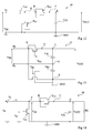
- the figure 12 represents an example of a charge pump energy recovery circuit 60.
- the circuit 60 comprises input terminals A 1 and A 2 receiving the AC voltage V 1N .
- Terminal A 2 is connected to ground GND.
- the terminal A 1 is connected to an armature of a capacitor C A1 whose other armature is connected to a node H.
- a diode-connected transistor T A1 is provided between the node H and the input terminal A 2 .
- the substrate, the gate and the source of transistor T A1 are connected to ground GND.
- the transistor T A1 may have the structure of the transistor M of the figure 2 .
- a diode-connected transistor T A2 is arranged between the node H and a node K.
- the transistor T A2 corresponds to the transistor M 'or M "according to the embodiments of the invention described above.
- the drain of the transistor T A2 are connected to the node H.
- the terminal CA, not shown, and the source of the transistor T A1 are connected to the node K.
- a capacitor C A2 is provided between the node K and the ground GND. OUT is the voltage between node K and ground GND.
- the figure 13 represents an example of a differential input energy recovery circuit 62.
- the circuit 62 comprises input terminals B 1 and B 2 receiving the AC voltage V 1N .
- a diode-connected transistor T B1 is provided between the input terminal B 2 and a node L.
- the transistor T B1 corresponds to the transistor M 'or M "according to the embodiments of the invention described above.
- gate and the drain of the transistor T B1 are connected to the terminal B 1.
- the terminal CA, not shown, and the source of the transistor T A1 are connected to the node L.
- a capacitor C B1 is arranged between the node L and a node O connected to the input terminal B 2.
- a capacitor C B2 is disposed between the node O and a node N.
- the node N is connected to the ground GND
- a diode-connected transistor T B2 is provided between the input terminal B 1 and the node N.
- the substrate, the gate and the drain of the transistor T B2 are connected to the ground GND
- the transistor T B2 can have the structure of the transistor M of the figure 2 .
- the voltage V OUT is taken between the nodes L and N.
- the figure 14 represents an example of an elevator chopper circuit 64.
- the circuit 64 comprises an input terminal E 1 receiving a voltage V E , for example a DC voltage.
- the terminal E 1 is connected to a node P by an inductance L.
- a transistor T C1 is provided between the node P and the ground GND.
- the gate of transistor T C1 receives a succession of voltage pulses V C whose frequency depends on the desired voltage V OUT .
- the oscillating voltage V 1N is the voltage between the node P and the ground GND.
- a diode-connected transistor T C2 is disposed between the node P and a node Q.
- the transistor T C2 corresponds to the transistor M 'or M "according to the embodiments of the invention described above.
- the drain of the transistor T C2 are connected to the node P.
- the terminal CA, not shown, and the source of the transistor T C2 are connected to the node Q.
- a capacitor C1 is arranged between the node Q and the ground GND. is provided across the capacitor C C1.
- the voltage V OUT corresponds to the voltage across the capacitor C C1.
- the operation of the circuit 64 during a cycle of control of transistor T C1 is schematically the following.
- the transistor T C1 When the transistor T C1 is conducting, the voltage V IN is substantially zero.
- Transistor T C2 is then blocked. At the moment when the transistor T C1 goes from the on state to the off state, the voltage V IN rises sharply temporarily due to the inductance L.
- the transistor T C2 becomes conducting resulting in the charge of the capacitor C
- the voltage V IN then decreases to V E causing the blocking of the transistor T C2 .
- the present invention also applies to a P-channel MOS transistor.
- the MOS transistor is, for example, made in a box.
- type N provided at a p-type doped layer.
- the N-type well forms the substrate of the transistor.
- P-type doped regions are provided in the N-type well and form the source and drain regions of the MOS transistor.
- the gate and the substrate are connected to the drain of the transistor.
Landscapes
- Engineering & Computer Science (AREA)
- Power Engineering (AREA)
- Metal-Oxide And Bipolar Metal-Oxide Semiconductor Integrated Circuits (AREA)
- Semiconductor Integrated Circuits (AREA)
Abstract
Description
- La présente invention concerne un circuit électronique comprenant un transistor MOSFET (de l'anglais Metal Oxide Semiconductor Field Effect Transistor) ou transistor MOS, monté en diode, dont l'une des bornes de puissance reçoit un signal oscillant, par exemple de signal alternatif.
- De nombreux circuits électroniques réalisent une fonction de conversion d'énergie. Le plus souvent, il s'agit d'une conversion d'un signal d'entrée alternatif, constitué d'une succession d'alternances positives et négatives, en un signal continu. L'un des circuits électroniques les plus simples pour réaliser cette fonction est le circuit redresseur simple alternance. Il est constitué d'un étage de redressement, suivi d'un étage de filtrage. L'étage de redressement peut comprendre une diode qui permet de conserver, par exemple, seulement les alternances positives du signal d'entrée. L'étage de filtrage peut comprendre un condensateur et fournit un signal sensiblement continu à partir des alternances positives.
- Pour réaliser un circuit redresseur de façon intégrée selon une technologie CMOS, la diode est généralement remplacée par un transistor MOS, monté en diode, c'est-à-dire dont la grille est reliée au drain. L'essentiel des pertes énergétiques du circuit redresseur réalisé de façon intégrée proviennent du transistor lorsque celui-ci est passant et dépendent du produit entre le courant traversant le transistor et la tension drain-source du transistor. Lorsque le transistor est passant, le courant de canal du transistor varie en fonction de la tension grille-source, c'est-à-dire de la tension drain-source. Pour réduire les pertes du circuit redresseur, il faut que la tension drain-source reste la plus faible possible lorsque le transistor est passant. Il est donc souhaitable que la tension de seuil du transistor soit la plus faible possible.
- De façon classique, le transistor MOS est réalisé dans et sur une couche d'un matériau semiconducteur polarisée par une source d'un potentiel de référence, par exemple la masse. Toutefois, avec une telle structure de transistor MOS, il s'avère difficile de diminuer de façon significative la tension de seuil du transistor. En outre, notamment lors des alternances négatives du signal d'entrée, on observe des pertes supplémentaires en raison du courant de fuite du transistor MOS à l'état bloqué et de la conduction de diodes parasites du transistor.
- La présente invention vise un circuit électronique comprenant un transistor MOS monté en diode dont l'une des bornes de puissance reçoit un signal oscillant, par exemple un signal alternatif, ayant des pertes réduites lorsque le transistor est passant.
- Selon un autre objet, l'invention vise à réduire les pertes dues au courant de fuite du transistor lorsque le transistor est bloqué.
- Selon un autre objet, la présente invention vise à réduire les pertes dues à la conduction de diodes parasites au cours de l'évolution du signal oscillant alors que le transistor est bloqué.
- Ainsi, un mode de réalisation de la présente invention prévoit un circuit intégré comportant une couche semiconductrice ; et un transistor MOS comprenant des première et deuxième bornes de puissance et un substrat isolé de la couche semiconductrice, la première borne de puissance étant destinée à recevoir un signal oscillant, la grille du transistor et le substrat étant reliés à la première borne de puissance.
- Selon un exemple de réalisation, le substrat correspond à une portion de la couche semiconductrice isolée du reste de la couche semiconductrice par une région dopée, la région dopée étant reliée à la deuxième borne de puissance.
- Selon un exemple de réalisation, la région dopée est d'un premier type de conductivité, les première et deuxième bornes de puissance comprenant des régions dopées supplémentaires du premier type de conductivité, la couche semiconductrice étant non dopée ou dopée d'un second type de conductivité, ladite portion de la couche semiconductrice s'étendant au moins entre les régions dopées supplémentaires.
- Selon un exemple de réalisation, le circuit comprend un filtre relié à la deuxième borne de puissance.
- Selon un exemple de réalisation, le transistor MOS est un transistor MOS à canal N.
- Un aspect de la présente invention vise un circuit électronique comprenant un circuit intégré tel que défini précédemment ; et une source d'un potentiel de référence reliée à la couche semiconductrice.
- Selon un exemple de réalisation, le circuit électronique comprend, en outre, un premier condensateur comprenant une première armature reliée à la première borne de puissance ; un second condensateur comprenant une seconde armature reliée à la deuxième borne de puissance et une troisième armature reliée à la source du potentiel de référence ; et un transistor MOS supplémentaire, monté en diode, comprenant une troisième borne de puissance reliée à la première borne de puissance et une quatrième borne de puissance reliée à la source du potentiel de référence.
- Selon un exemple de réalisation, le circuit électronique comprend, en outre, un premier condensateur comprenant une première armature reliée à la seconde borne de puissance et une deuxième armature ; un second condensateur comprenant une troisième armature reliée à la deuxième armature et une troisième armature reliée à la source du potentiel de référence ; et un transistor MOS supplémentaire, monté en diode, comprenant une troisième borne de puissance reliée à la première borne de puissance et une quatrième borne de puissance reliée à la source du potentiel de référence.
- Selon un exemple de réalisation, le circuit électronique comprend, en outre, une source d'alimentation ; une inductance reliant la source d'alimentation à la première borne de puissance ; un transistor MOS supplémentaire comprenant une troisième borne de puissance reliée à la première borne de puissance et une quatrième borne de puissance reliée à la source du potentiel de référence ; une source d'une succession d'impulsions de tension à la grille du transistor MOS supplémentaire ; et un condensateur comprenant une première armature reliée à la deuxième borne de puissance et une deuxième armature reliée à la source du potentiel de référence.
- Ces objets, caractéristiques et avantages, ainsi que d'autres seront exposés en détail dans la description suivante de modes de réalisation particuliers faite à titre non-limitatif en relation avec les figures jointes parmi lesquelles :
- la
figure 1 représente de façon schématique un exemple classique d'un circuit redresseur ; - la
figure 2 est une coupe schématique d'un transistor MOS classique monté en diode ; - la
figure 3 représente, de façon schématique, un exemple de circuit redresseur mettant en oeuvre le transistor MOS monté en diode de lafigure 2 ; - la
figure 4 est une vue analogue à lafigure 3 , certaines diodes parasites du transistor MOS monté en diode ayant été représentées ; - la
figure 5 représente un exemple de réalisation d'un transistor MOS monté en diode selon l'invention ; - la
figure 6 représente un circuit redresseur muni du transistor MOS monté en diode de lafigure 5 ; - la
figure 7 représente des courbes d'évolution du courant de canal du transistor MOS monté en diode des circuits desfigures 4 et6 en fonction de la tension drain-source du transistor ; - la
figure 8 représente des courbes d'évolution du courant de fuite du transistor MOS monté en diode des circuits desfigures 4 et6 en fonction de la tension d'entrée ; - la
figure 9 représente des courbes d'évolution du courant au drain du transistor MOS monté en diode des circuits desfigures 4 et6 en fonction de la tension d'entrée ; - la
figure 10 représente un autre exemple de réalisation d'un transistor MOS monté en diode selon l'invention ; - la
figure 11 représente, de façon schématique, un exemple de circuit redresseur mettant en oeuvre le transistor MOS de lafigure 10 ; et - les
figures 12 à 14 représentent d'autres exemples de circuits munis du transistor MOS de lafigure 4 . - Par souci de clarté, de mêmes éléments ont été désignés par de mêmes références aux différentes figures et, de plus, comme cela est habituel dans la représentation des circuits intégrés, les diverses figures ne sont pas tracées à l'échelle. Dans la suite de la description, on appelle bornes de puissance d'un transistor MOS la source et le drain du transistor. En outre, dans la suite de la description, on considère un circuit recevant un signal oscillant. Un signal oscillant est un signal qui passe alternativement d'une valeur extrême haute à une valeur extrême basse. Les valeurs extrêmes haute et basse peuvent être de signes opposés. Le signal est alors dit alternatif. Il comprend alors successivement une alternance positive, une alternance négative, une alternance positive, une alternance négative, etc. Le signal oscillant peut être périodique.
- La
figure 1 représente, de façon schématique, un circuit redresseur 10 simple alternance avec filtre à condensateur. Le circuit 10 comprend deux bornes d'entrée N1 et N2 entre lesquelles est appliquée une tension oscillante VIN, par exemple une tension alternative. A titre d'exemple, la tension alternative VIN est une tension sinusoïdale. La tension VIN peut être fournie à partir d'un signal radiofréquence capté par une antenne. De façon générale, la tension alternative VIN est une tension périodique, comprenant, pour chaque période, une alternance positive et une alternance négative. La borne d'entrée N2 est reliée à une source d'un potentiel de référence, par exemple la masse GND. Le circuit 10 comprend une diode Diode dont l'anode est reliée à la borne d'entrée N1 et dont la cathode est reliée à un noeud E. Un condensateur C est disposé entre le noeud E et un noeud F relié à la masse GND. Une résistance R est disposée en parallèle aux bornes du condensateur C. On désigne par la référence VOUT la tension entre les noeuds E et F. - Lorsque le circuit redresseur 10 doit être réalisé de façon intégrée selon une technologie CMOS, la fonction remplie par la diode Diode du circuit 10, est réalisée par un transistor MOS, monté en diode.
- La
figure 2 représente un exemple d'une structure classique d'un transistor MOS M monté en diode formé au niveau d'une couche 12 d'un matériau semiconducteur, par exemple du silicium monocristallin dopé de type P, ayant une surface supérieure 13. A titre d'exemple, le transistor M est un transistor à canal N. Le transistor MOS comprend une portion isolante 14, par exemple en oxyde de silicium, recouvrant la couche 12. Une portion 16 d'un matériau semiconducteur, par exemple du silicium polycristallin, recouvre la portion isolante 14. Des régions dopées de type N 18, 20 sont prévues dans la couche 12 de part et d'autre de la portion isolante 14. Les régions 18 et 20 s'étendent éventuellement partiellement sous la portion isolante 14. Une région 22 dopée de type P s'étend dans la couche 12 depuis la surface 13. La région 22 est plus fortement dopée que la couche 12. La portion isolante 14 constitue l'isolant de grille du transistor M et la portion 16 constitue la grille du transistor M. La région 18 constitue la région de source du transistor M et la région 20 constitue la région de drain du transistor M. - Les connexions des éléments du transistor M sont réalisées par des pistes et vias conducteurs non représentés en détail. On a schématiquement représenté en
figure 2 une borne G connectée à la portion 16, une borne S connectée à la région de source 18 et une borne D connectée à la région de drain. Une borne B est connectée à la région 22 et permet de polariser la couche 12. Dans la suite de la description, on appelle indifféremment grille du transistor M la portion 16 ou la borne G, source du transistor M la région 18 ou la borne S et drain du transistor M la région 20 ou la borne D. Le transistor M étant monté en diode, la grille G est reliée au drain D. - En
figure 2 , on a représenté deux diodes parasites intrinsèques au transistor M. Une première diode parasite DiodeBS correspond à la jonction entre la couche 12 et la région de source 18. Une seconde diode parasite DiodeBD correspond à la jonction entre la couche 12 et la région de drain 20. - La
figure 3 représente un circuit redresseur 25 analogue au circuit 10 de lafigure 1 dans lequel la fonction remplie par la diode Diode est réalisée à partir du transistor M monté en diode de lafigure 2 . Le drain D du transistor M est relié à la borne d'entrée N1. La source S du transistor M est reliée au noeud E. Le substrat B du transistor M est polarisé à la masse GND. Dans la suite de la description, on appelle VDS la tension entre le drain D et la source S du transistor M, VGS la tension entre la grille G et la source S du transistor M et IN1 est le courant à la borne d'entrée N1. Le circuit redresseur 25 est destiné à être connecté à d'autres circuits au niveau des noeuds E et F. - La tension de seuil Vt0 du transistor M du circuit 10 est donnée par la relation suivante :

où C1, C2 et C3 sont des constantes. En raison du filtrage réalisé par le condensateur C et la résistance R, la tension VOUT varie peu de sorte que la tension de seuil Vt0 peut être considéré comme sensiblement constante. - Les pertes du circuit 25 dues à la conduction du transistor M sont proportionnelles au produit de la tension VDS, égale à la tension VGS, et du courant IDS. Ces pertes se produisent, en régime établi, lorsque la tension VGS est supérieure à la tension de seuil Vt0. Pour minimiser les pertes dues à la conduction du transistor M, il est souhaitable que la tension de seuil Vt0 du transistor M soit la plus faible possible. La relation (1) montre que la tension de seuil Vt0 est directement imposée par la valeur de la tension VOUT qui est généralement fixée par l'application envisagée du circuit redresseur 25. Il s'avère donc difficile de réduire la tension de seuil Vt0. En outre, le transistor M présente un courant de fuite à l'état bloqué, notamment lors des alternances négatives de la tension VIN, qui augmente les pertes du circuit 25. De façon générale, plus la tension de seuil d'un transistor MOS est faible, plus le courant de fuite est important. Il n'est donc pas possible avec le circuit 25 de réduire simultanément la tension de seuil Vt0 et le courant de fuite du transistor MOS.
- La
figure 4 représente le circuit redresseur 25 de lafigure 3 dans lequel les diodes parasites DiodeBS et DiodeBD du transistor M ont été représentées. La diode parasite DiodeBD s'étend entre les bornes N1 et N2, l'anode de la diode DiodeBD étant connectée à la borne d'entrée N2. La diode parasite DiodeBS s'étend entre les noeuds E et F, l'anode de la diode DiodeBS étant connectée au noeud F. Sur chaque alternance négative de la tension VIN, la diode parasite DiodeBD peut devenir passante. Ceci augmente les pertes du circuit 25. Lorsque la diode parasite DiodeBD est bloquée, l'impédance d'entrée du circuit 25 est élevée. Toutefois, lorsque la diode parasite DiodeBD devient passante, l'impédance d'entrée du circuit 25 chute, ce qui peut être pénalisant pour certaines applications. Il peut donc être nécessaire de limiter l'amplitude de la tension VIN pour éviter la chute de l'impédance d'entrée du circuit 25. - La
figure 5 représente la structure d'un transistor M' monté en diode selon un exemple de réalisation de l'invention. Par rapport au transistor M représenté enfigure 2 , le transistor M' comprend une structure 30 d'isolement de substrat qui délimite une partie 32 de la couche semiconductrice 12 autour des régions de source et de drain 18, 20 du transistor M'. La portion 32, électriquement isolée du reste de la couche 12, est appelée substrat 32 (en anglais bulk ou body) du transistor M' dans la suite de la description. Le dopage de la région 32 est choisi suffisamment faible pour que la tension de seuil du transistor MOS soit nettement inférieure à 0,6 V, de préférence comprise entre 0,1 et 0,3 V. La structure 30 d'isolement de substrat comprend une région enterrée 34 de type N située en profondeur dans la couche 12 et s'étendant sous les régions 18, 20 et 22. La structure 30 d'isolement de substrat comprend, en outre, une paroi latérale 36 correspondant à une région de type N s'étendant depuis la surface 13 de la couche 12 jusqu'à la région enterrée 34 et entourant les régions 18, 20 et 22. Une région 38, de type N, plus fortement dopée que la région 36 s'étend dans la région 36 depuis la surface 13. Une borne de polarisation CA de la structure 30 d'isolement de substrat est connectée à la région 38. Une région 39 dopée de type P s'étend dans la couche 12 depuis la surface 13 à l'extérieur de la structure 30 d'isolement de substrat. Une borne W est connectée à la région 39 et permet de polariser le reste de la couche 12. Le transistor M' étant monté en diode, la grille G est reliée au drain D. En outre, la borne B de polarisation du substrat 32 est reliée au drain D et la borne CA de polarisation de la structure 30 d'isolement de substrat est reliée à la source S. La borne W de polarisation de la couche 12 est reliée à la source du potentiel de référence GND. - En
figure 5 , on a représenté schématiquement les diodes parasites intrinsèques du transistor M'. La diode DiodeBS correspond à la jonction entre le substrat 32 du transistor M' et la région de source 18. La diode DiodeBD correspond à la jonction entre le substrat 32 du transistor M' et la région de drain 20. La diode DiodeW correspond à la jonction entre la structure 30 d'isolement de substrat et la partie de la couche 12 à l'extérieur de la structure 30 d'isolement de substrat. La diode DiodeISO correspond à la jonction entre le substrat 32 du transistor M' et la structure 30 d'isolement de substrat. - La
figure 6 représente un circuit redresseur 40 analogue au circuit redresseur 25 de lafigure 3 dans lequel le transistor M' est utilisé. Les diodes parasites DiodeISO, DiodeBS et DiodeW du transistor M' sont représentées. Les diodes DiodeISO et DiodeBS s'étendent entre le drain D et le noeud E, les anodes des diodes DiodeISO et DiodeBS étant reliées au drain D. La diode DiodeW s'étend entre les noeuds E et F, l'anode de la diode DiodeW étant reliée au noeud F. Le substrat B étant relié au drain D du transistor M', la jonction entre le substrat 32 et la région de drain 20 est court-circuitée de sorte que la diode parasite DiodeBS n'intervient pas. - La demanderesse a mis en évidence que pour le transistor M' connecté comme cela est représenté en
figure 6 , la tension de seuil Vt1 du transistor M' est donnée par la relation suivante :
- La tension de seuil Vt1 varie donc en fonction de la tension VGS, c'est-à-dire en fonction de la tension VDS. En particulier Vt1 diminue lorsque que la tension VGS est positive et croît. La tension de seuil Vt1 pour laquelle le transistor M' devient passant lors d'une alternance positive de la tension VIN est inférieure à la tension de seuil Vt0 définie par la relation (1). Cette tension de seuil du transistor MOS est en tout cas nettement inférieure à la tension de conduction en direct d'une diode bipolaire (environ 0,6 V).
- La
figure 7 représente des courbes 41, 42 d'évolution du courant IDS en fonction de la tension VDS. La courbe 41 correspond au circuit 25 de lafigure 4 pour VOUT égal à 1 V et la courbe 42 correspond au circuit 40 de lafigure 6 . La tension de seuil Vt1 du transistor M' selon le présent exemple de réalisation de l'invention étant plus faible que la tension de seuil Vt0 du transistor M, pour un même courant IDS, la tension VDS du circuit de lafigure 6 est inférieure à celle du circuit de lafigure 4 . Les pertes en conduction du circuit 40 sont ainsi diminuées par rapport au circuit 25. En outre, les diodes parasites DiodeISO et DiodeBS du transistor M' ne peuvent pas devenir passantes. - La
figure 8 représente des courbes d'évolution 44, 46 du courant de fuite respectivement des transistors M et M' lors d'une alternance négative de la tension VIN. - Pour le circuit 25 de la
figure 4 , la tension de seuil Vt0 du transistor M ne varie sensiblement pas pendant une alternance négative de la tension VIN (relation (1)). Tout au long de l'alternance négative, la tension VGS est négative et supérieure, en valeur absolue, à VOUT. La tension Vt1 est donc supérieure à la tension de seuil Vt0 tout au long de l'alternance négative. Le courant de fuite d'un transistor MOS diminuant lorsque la tension de seuil du transistor augmente, le courant de fuite du transistor M' est inférieur au courant de fuite du transistor M d'au moins un facteur 2 sur la majeure partie de l'alternance négative. - La
figure 9 représente des courbes 48, 50 d'évolution du courant IN1 à la borne d'entrée N1 en fonction de la tension VIN lors d'une alternance négative de la tension VIN. La courbe 48 correspond au circuit 25 de lafigure 4 et la courbe 50 correspond au circuit 40 de lafigure 6 . La courbe 48 comprend une première partie 51 fortement croissante suivie d'une seconde partie 52 très faiblement croissante. La courbe 50 ne comprend qu'une partie très faiblement croissante. Pour le circuit 25, au cours de l'alternance négative, la diode parasite DiodeBD tend à être passante ce qui se traduit par un courant IN1 négatif qui augmente fortement, en valeur absolue, lorsque la tension VIN négative augmente, en valeur absolue (partie 51 de la courbe 48). Lorsque la diode parasite DiodeBD n'est plus passante, le courant IN1 correspond au courant de fuite du transistor M pendant l'alternance négative (partie 52 de la courbe 48). Pour le circuit 40, il n'y a plus de diode parasite entre les bornes d'entrée N1 et N2. La courbe 50 traduit bien le fait que le courant ID est seulement égal au courant de fuite du transistor M' tout au long de l'alternance négative qui est inférieur au courant de fuite du transistor M. Les pertes supplémentaires lors d'une alternance négative de la tension VIN sont donc diminuées pour le circuit 40 par rapport au circuit 25. En outre, l'absence de diode parasite pour le transistor M' entre les bornes d'entrée N1 et N2 fait qu'il n'y a plus de risque de chute de l'impédance d'entrée du circuit 40. De ce fait, il n'y a plus de contraintes concernant l'amplitude de la tension VIN lors de l'alternance négative et il n'y a pas de risque de perte de modulation. - La
figure 10 représente un autre exemple d'une structure de transistor MOS M" monté en diode selon l'invention. La structure du transistor M" est semblable à celle du transistor M' de lafigure 5 à la différence que la borne CA est connectée au drain D et non à la source S. La borne W est, comme pour le transistor M', reliée à la masse GND. L'expression de la tension de seuil du transistor M" est donnée par la relation (2). On retrouve les mêmes avantages concernant la diminution de la tension seuil que pour l'exemple de réalisation décrit précédemment en relation avec lafigure 5 . - La
figure 11 représente un circuit 55 analogue au circuit 40 de lafigure 6 à la différence que le transistor M' est remplacé par le transistor M". La diode parasite DiodeW est alors située entre les bornes d'entrée N1 et N2. On retrouve alors les inconvénients du circuit 10 de lafigure 4 avec des pertes dues à la conduction de la diode parasite DiodeW au cours des alternances négatives de la tension V1N. - Bien que le transistor MOS M' selon le présent exemple de réalisation de l'invention ait été décrit pour un circuit redresseur 40, le transistor M' ou M" peut être utilisé pour d'autres types de circuits électroniques mettant en oeuvre un transistor MOS monté en diode dont le drain reçoit un signal oscillant.
- Les
figures 12 à 14 représentent d'autres exemples de circuits électroniques dans lesquels le transistor MOS M' ou M" selon les exemples de réalisation de l'invention décrits précédemment peut être utilisé. - La
figure 12 représente un exemple de circuit 60 récupérateur d'énergie à pompes de charge. Le circuit 60 comprend des bornes d'entrée A1 et A2 recevant la tension alternative V1N. La borne A2 est reliée à la masse GND. La borne A1 est connectée à une armature d'un condensateur CA1 dont l'autre armature est reliée à un noeud H. Un transistor TA1 monté en diode est prévu entre le noeud H et la borne d'entrée A2. Le substrat, la grille et la source du transistor TA1 sont reliés à la masse GND. Le transistor TA1 peut avoir la structure du transistor M de lafigure 2 . Un transistor TA2, monté en diode, est disposé entre le noeud H et un noeud K. Le transistor TA2 correspond au transistor M' ou M" selon les exemples de réalisation de l'invention décrits précédemment. Le substrat, la grille et le drain du transistor TA2 sont reliés au noeud H. La borne CA, non représentée, et la source du transistor TA1 sont reliées au noeud K. Un condensateur CA2 est prévu entre le noeud K est la masse GND. La tension VOUT correspond à la tension entre le noeud K et la masse GND. - La
figure 13 représente un exemple de circuit 62 de récupération d'énergie à entrée différentielle. Le circuit 62 comprend des bornes d'entrée B1 et B2 recevant la tension alternative V1N. Un transistor TB1 monté en diode est prévu entre la borne d'entrée B2 et un noeud L. Le transistor TB1 correspond au transistor M' ou M" selon les exemples de réalisation de l'invention décrits précédemment. Le substrat, la grille et le drain du transistor TB1 sont reliés à la borne B1. La borne CA, non représentée, et la source du transistor TA1 sont reliées au noeud L. Un condensateur CB1 est disposé entre le noeud L et un noeud O relié à la borne d'entrée B2. Un condensateur CB2 est disposé entre le noeud O et un noeud N. Le noeud N est relié à la masse GND. Un transistor TB2 monté en diode est prévu entre la borne d'entrée B1 et le noeud N. Le substrat, la grille et le drain du transistor TB2 sont reliés à la masse GND. Le transistor TB2 peut avoir la structure du transistor M de lafigure 2 . La tension VOUT est prise entre les noeuds L et N. - La
figure 14 représente un exemple de circuit 64 hacheur élévateur. Le circuit 64 comprend une borne d'entrée E1 recevant une tension VE, par exemple, une tension continue. La borne E1 est reliée à un noeud P par une inductance L. Un transistor TC1 est prévu entre le noeud P et la masse GND. La grille du transistor TC1 reçoit une succession d'impulsions de tension VC dont la fréquence dépend de la tension VOUT désirée. La tension V1N oscillante est la tension entre le noeud P et la masse GND. Un transistor TC2, monté en diode, est disposé entre le noeud P et un noeud Q. Le transistor TC2 correspond au transistor M' ou M" selon les exemples de réalisation de l'invention décrits précédemment. Le substrat, la grille et le drain du transistor TC2 sont reliés au noeud P. La borne CA, non représentée, et la source du transistor TC2 sont reliées au noeud Q. Un condensateur CC1 est disposé entre le noeud Q et la masse GND. Une résistance RL est prévue aux bornes du condensateur CC1. La tension VOUT correspond à la tension aux bornes du condensateur CC1. Le fonctionnement du circuit 64 au cours d'un cycle de commande du transistor TC1 est schématiquement le suivant. Lorsque le transistor TC1 est passant, la tension VIN est sensiblement nulle. Le transistor TC2 est alors bloqué. Au moment où le transistor TC1 passe de l'état passant à l'état bloqué, la tension VIN s'élève fortement de façon temporaire en raison de l'inductance L. Le transistor TC2 devient passant entraînant la charge du condensateur C. La tension VIN diminue alors jusqu'à VE entraînant le blocage du transistor TC2. - Des modes de réalisation particuliers de la présente invention ont été décrits. Diverses variantes et modifications apparaîtront à l'homme de l'art. En particulier, bien que les exemples de réalisation décrits précédemment concernent un transistor MOS à canal N, la présente invention s'applique également à un transistor MOS à canal P. Dans ce cas, le transistor MOS est, par exemple, réalisé dans un caisson de type N prévu au niveau d'une couche dopée de type P. Le caisson de type N forme le substrat du transistor. Des régions dopées de type P sont prévues dans le caisson de type N et forment les régions de source et de drain du transistor MOS. La grille et le substrat sont reliés au drain du transistor.
Claims (9)
- Circuit intégré (40 ; 60 ; 62 ; 64) comportant :une couche semiconductrice (12) ; etun transistor MOS (M' ; M" ; TA2 ; TB1 ; TC2) comprenant des première et deuxième bornes de puissance (S, D) et un substrat (B) isolé de la couche semiconductrice, la première borne de puissance (D) étant destinée à recevoir un signal oscillant (V1N), la grille (G) du transistor et le substrat étant reliés à la première borne de puissance, ledit transistor MOS étant conçu pour que sa tension de seuil soit inférieure à 0,6 V, de préférence comprise entre 0,1 et 0,3 V.
- Circuit intégré selon la revendication 1, dans lequel le substrat (B) correspond à une portion (32) de la couche semiconductrice (12) isolée du reste de la couche semiconductrice par une région dopée (30), la région dopée étant reliée à la deuxième borne de puissance (S).
- Circuit intégré selon la revendication 2, dans lequel la région dopée (30) est d'un premier type de conductivité, les première et deuxième bornes de puissance (S, D) comprenant des régions dopées supplémentaires (18, 20) du premier type de conductivité, la couche semiconductrice (12) étant non dopée ou dopée d'un second type de conductivité, ladite portion (32) de la couche semiconductrice s'étendant au moins entre les régions dopées supplémentaires.
- Circuit intégré selon l'une quelconque des revendications 1 à 3, comprenant un filtre (R, C) relié à la deuxième borne de puissance (S).
- Circuit intégré selon l'une quelconque des revendications 1 à 4, dans lequel le transistor MOS (M' ; M" ; TA2 ; TB1 ; TC2) est un transistor MOS à canal N.
- Circuit électronique (40 ; 60 ; 62 ; 64) comprenant :un circuit intégré selon l'une quelconque des revendications 1 à 5 ; etune source d'un potentiel de référence (GND) reliée à la couche semiconductrice (12).
- Circuit électronique (60) selon la revendication 6, comprenant, en outre :un premier condensateur (CA1) comprenant une première armature reliée à la première borne de puissance (D) ;un second condensateur (CA2) comprenant une seconde armature reliée à la deuxième borne de puissance (S) et une troisième armature reliée à la source du potentiel de référence (GND) ; etun transistor MOS supplémentaire (TA1), monté en diode, comprenant une troisième borne de puissance reliée à la première borne de puissance et une quatrième borne de puissance reliée à la source du potentiel de référence.
- Circuit électronique (62) selon la revendication 6, comprenant, en outre :un premier condensateur (CB1) comprenant une première armature reliée à la seconde borne de puissance (S) et une deuxième armature ;un second condensateur (CB2) comprenant une troisième armature reliée à la deuxième armature et une troisième armature reliée à la source du potentiel de référence (GND) ; etun transistor MOS supplémentaire (TB2), monté en diode, comprenant une troisième borne de puissance reliée à la première borne de puissance et une quatrième borne de puissance reliée à la source du potentiel de référence.
- Circuit électronique (64) selon la revendication 6, comprenant, en outre :une source d'alimentation (VE) ;une inductance (L) reliant la source d'alimentation à la première borne de puissance (D) ;un transistor MOS supplémentaire (TC1) comprenant une troisième borne de puissance reliée à la première borne de puissance et une quatrième borne de puissance reliée à la source du potentiel de référence (GND) ;une source d'une succession d'impulsions de tension (VC) à la grille du transistor MOS supplémentaire ; etun condensateur (CC1) comprenant une première armature reliée à la deuxième borne de puissance (S) et une deuxième armature reliée à la source du potentiel de référence.
Applications Claiming Priority (1)
| Application Number | Priority Date | Filing Date | Title |
|---|---|---|---|
| FR0854555 | 2008-07-04 |
Publications (2)
| Publication Number | Publication Date |
|---|---|
| EP2141741A2 true EP2141741A2 (fr) | 2010-01-06 |
| EP2141741A3 EP2141741A3 (fr) | 2012-08-15 |
Family
ID=40263168
Family Applications (1)
| Application Number | Title | Priority Date | Filing Date |
|---|---|---|---|
| EP09164596A Withdrawn EP2141741A3 (fr) | 2008-07-04 | 2009-07-03 | Circuit électronique comprenant un transistor MOS monté en diode à rendement amélioré |
Country Status (2)
| Country | Link |
|---|---|
| US (1) | US8445947B2 (fr) |
| EP (1) | EP2141741A3 (fr) |
Cited By (1)
| Publication number | Priority date | Publication date | Assignee | Title |
|---|---|---|---|---|
| FR3041838A1 (fr) * | 2015-09-28 | 2017-03-31 | Commissariat Energie Atomique | Circuit electronique elementaire pour etage d'amplification ou de recopie de signaux analogiques |
Families Citing this family (8)
| Publication number | Priority date | Publication date | Assignee | Title |
|---|---|---|---|---|
| EP2384518B1 (fr) * | 2009-01-06 | 2019-09-04 | STMicroelectronics N.V. | Structures de diode à effet de champ à auto-amorçage et procédés correspondants |
| JP2011138214A (ja) * | 2009-12-25 | 2011-07-14 | Toshiba Corp | 半導体集積回路装置 |
| WO2011108374A1 (fr) * | 2010-03-05 | 2011-09-09 | Semiconductor Energy Laboratory Co., Ltd. | Dispositif à semi-conducteur et procédé de fabrication de dispositif à semi-conducteur |
| JP5587135B2 (ja) * | 2010-10-28 | 2014-09-10 | ルネサスエレクトロニクス株式会社 | 無線通信用半導体装置 |
| DE102010062677A1 (de) * | 2010-12-09 | 2012-06-14 | Robert Bosch Gmbh | Generatorvorrichtung zur Spannungsversorgung eines Kraftfahrzeugs |
| US9553087B1 (en) * | 2015-11-02 | 2017-01-24 | Taiwan Semiconductor Manufacturing Company Ltd. | Semiconductor device |
| US20200194459A1 (en) * | 2018-12-18 | 2020-06-18 | Vanguard International Semiconductor Corporation | Semiconductor devices and methods for fabricating the same |
| CN112421969A (zh) * | 2020-06-22 | 2021-02-26 | 杭州炬华科技股份有限公司 | 一种增强型阻容电源电路 |
Family Cites Families (30)
| Publication number | Priority date | Publication date | Assignee | Title |
|---|---|---|---|---|
| US5240865A (en) * | 1990-07-30 | 1993-08-31 | Texas Instruments Incorporated | Method of forming a thyristor on an SOI substrate |
| JP2771729B2 (ja) | 1992-04-16 | 1998-07-02 | 三菱電機株式会社 | チャージポンプ回路 |
| US5801420A (en) * | 1994-09-08 | 1998-09-01 | Fuji Electric Co. Ltd. | Lateral semiconductor arrangement for power ICS |
| US6285240B1 (en) * | 1999-01-14 | 2001-09-04 | Macronix International Co., Ltd. | Low threshold MOS two phase negative charge pump |
| TW419806B (en) * | 1999-01-25 | 2001-01-21 | Winbond Electronics Corp | Electrostatic discharge device for circuit with an operating voltage larger than the supplied voltage |
| JP4617527B2 (ja) * | 1999-04-08 | 2011-01-26 | 株式会社デンソー | 回路装置 |
| TW451423B (en) * | 2000-02-01 | 2001-08-21 | Ind Tech Res Inst | Latch-up structure for improving CMOS processing using latch-up ion implantation and the manufacturing method thereof |
| US6492208B1 (en) * | 2000-09-28 | 2002-12-10 | Taiwan Semiconductor Manufacturing Company | Embedded SCR protection device for output and input pad |
| US6455902B1 (en) * | 2000-12-06 | 2002-09-24 | International Business Machines Corporation | BiCMOS ESD circuit with subcollector/trench-isolated body mosfet for mixed signal analog/digital RF applications |
| US6537921B2 (en) | 2001-05-23 | 2003-03-25 | Vram Technologies, Llc | Vertical metal oxide silicon field effect semiconductor diodes |
| JP4124981B2 (ja) * | 2001-06-04 | 2008-07-23 | 株式会社ルネサステクノロジ | 電力用半導体装置および電源回路 |
| US6900091B2 (en) * | 2002-08-14 | 2005-05-31 | Advanced Analogic Technologies, Inc. | Isolated complementary MOS devices in epi-less substrate |
| US6934171B2 (en) * | 2003-09-26 | 2005-08-23 | Lsi Logic Corporation | Semiconductor integrated circuit having voltage-down circuit regulator and charge sharing |
| WO2005057628A2 (fr) * | 2003-12-08 | 2005-06-23 | University Of South Florida | Procede et appareil de reduction des fuites dans les circuits integres |
| FR2864343A1 (fr) * | 2003-12-19 | 2005-06-24 | St Microelectronics Sa | Triac fonctionnant dans les quadrants q1 et q4 |
| US7304354B2 (en) * | 2004-02-17 | 2007-12-04 | Silicon Space Technology Corp. | Buried guard ring and radiation hardened isolation structures and fabrication methods |
| JP4593126B2 (ja) * | 2004-02-18 | 2010-12-08 | 三菱電機株式会社 | 半導体装置 |
| US7127216B2 (en) * | 2004-07-06 | 2006-10-24 | Avago Technologies Wireless Ip (Singapore) Pte. Ltd. | Integrated circuit and method for receiving and transmitting signals of different frequency bands |
| JP4566692B2 (ja) * | 2004-10-28 | 2010-10-20 | シャープ株式会社 | 発光ダイオード駆動装置及びそれを備えた光伝送装置 |
| JP4703196B2 (ja) | 2005-01-18 | 2011-06-15 | 株式会社東芝 | 半導体装置 |
| CN100568487C (zh) | 2005-02-16 | 2009-12-09 | 株式会社日立制作所 | 电子标签芯片 |
| US7500118B2 (en) | 2005-03-28 | 2009-03-03 | Akros Silicon Inc. | Network device with power potential rectifier |
| KR100724563B1 (ko) * | 2005-04-29 | 2007-06-04 | 삼성전자주식회사 | 다중 일함수 금속 질화물 게이트 전극을 갖는 모스트랜지스터들, 이를 채택하는 씨모스 집적회로 소자들 및그 제조방법들 |
| US7317229B2 (en) * | 2005-07-20 | 2008-01-08 | Applied Materials, Inc. | Gate electrode structures and methods of manufacture |
| KR100639231B1 (ko) * | 2005-12-30 | 2006-11-01 | 주식회사 하이닉스반도체 | 정전기 방전 보호 회로 |
| JP2007220755A (ja) * | 2006-02-14 | 2007-08-30 | Toshiba Corp | 半導体装置及びその製造方法 |
| US20070228425A1 (en) * | 2006-04-04 | 2007-10-04 | Miller Gayle W | Method and manufacturing low leakage MOSFETs and FinFETs |
| EP1944801A1 (fr) * | 2007-01-10 | 2008-07-16 | Interuniversitair Microelektronica Centrum | Procédés de fabrication d'un dispositif CMOS à travail d'extraction dual |
| JP4989309B2 (ja) * | 2007-05-18 | 2012-08-01 | 株式会社半導体エネルギー研究所 | 液晶表示装置 |
| US7745292B2 (en) * | 2007-10-15 | 2010-06-29 | Infineon Technologies Ag | Method for fabricating a semiconductor gate structure |
-
2009
- 2009-07-02 US US12/497,210 patent/US8445947B2/en active Active
- 2009-07-03 EP EP09164596A patent/EP2141741A3/fr not_active Withdrawn
Cited By (3)
| Publication number | Priority date | Publication date | Assignee | Title |
|---|---|---|---|---|
| FR3041838A1 (fr) * | 2015-09-28 | 2017-03-31 | Commissariat Energie Atomique | Circuit electronique elementaire pour etage d'amplification ou de recopie de signaux analogiques |
| WO2017055709A1 (fr) * | 2015-09-28 | 2017-04-06 | Commissariat A L'energie Atomique Et Aux Energies Alternatives | Circuit electronique elementaire pour etage d'amplification ou de recopie de signaux analogiques |
| US10644690B2 (en) | 2015-09-28 | 2020-05-05 | Commissariat à l'énergie atomique et aux énergies alternatives | Elementary electronic circuit for stage of amplification or repeat of analog signals |
Also Published As
| Publication number | Publication date |
|---|---|
| US8445947B2 (en) | 2013-05-21 |
| US20100034000A1 (en) | 2010-02-11 |
| EP2141741A3 (fr) | 2012-08-15 |
Similar Documents
| Publication | Publication Date | Title |
|---|---|---|
| FR2987496A1 (fr) | Circuit de protection contre les decharges electrostatiques | |
| FR2714547A1 (fr) | Système de commande d'actionneurs à courant continu en électronique de puissance. | |
| WO1998024172A2 (fr) | Dispositif de redressement de tension a composants integres | |
| EP4456362A1 (fr) | Circuit de protection contre les surtensions | |
| FR2694851A1 (fr) | Circuit de tirage vers un état déterminé d'une entrée de circuit intégré. | |
| US20100034000A1 (en) | Electronic circuit having a diode-connected mos transistor with an improved efficiency | |
| FR2858493A1 (fr) | Circuit d'attaque a autoelevation | |
| EP2913849B1 (fr) | Dispositif electronique avec transistor hemt polarisé en inverse | |
| EP0543745B1 (fr) | Transistor MOS à zener de protection intégrée | |
| FR2477338A1 (fr) | Circuit de sortie empeche de se bloquer du fait d'impulsions de tension produites par une charge inductive | |
| EP4358126A1 (fr) | Dispositif electronique | |
| FR3095891A1 (fr) | Circuit électronique | |
| EP0921571B1 (fr) | Dispositif de protection contre des décharges électrostatiques à faible niveau de seuil | |
| EP2966687B1 (fr) | Capteur d'images cmos | |
| EP0881682B1 (fr) | Dispositif de protection contre des surtensions d'un transistor MOS de puissance intégré | |
| FR2737065A1 (fr) | Dispositif semiconducteur incluant un amplificateur de puissance et appareil de telecommunication mobile incluant un tel dispositif semiconducteur | |
| FR3140987A1 (fr) | Transistor de puissance | |
| EP4102701A1 (fr) | Convertisseur de puissance | |
| FR3131981A1 (fr) | Dispositif de protection contre les décharges électrostatiques | |
| FR2545989A1 (fr) | Transistor a effet de champ, fonctionnant en regime d'enrichissement | |
| EP4086973A1 (fr) | Dispositif de suppression de tensions transitoires unidirectionnel sans conduction en direct | |
| EP3754697A1 (fr) | Composant monolithique comportant un transistor de puissance au nitrure de gallium | |
| EP4358406A2 (fr) | Circuit de protection contre les surchauffes | |
| EP4357877A1 (fr) | Circuit regulateur de tension | |
| EP4297090A1 (fr) | Dispositif microélectronique à deux transistors à effet de champ |
Legal Events
| Date | Code | Title | Description |
|---|---|---|---|
| PUAI | Public reference made under article 153(3) epc to a published international application that has entered the european phase |
Free format text: ORIGINAL CODE: 0009012 |
|
| AK | Designated contracting states |
Kind code of ref document: A2 Designated state(s): AT BE BG CH CY CZ DE DK EE ES FI FR GB GR HR HU IE IS IT LI LT LU LV MC MK MT NL NO PL PT RO SE SI SK SM TR |
|
| PUAL | Search report despatched |
Free format text: ORIGINAL CODE: 0009013 |
|
| AK | Designated contracting states |
Kind code of ref document: A3 Designated state(s): AT BE BG CH CY CZ DE DK EE ES FI FR GB GR HR HU IE IS IT LI LT LU LV MC MK MT NL NO PL PT RO SE SI SK SM TR |
|
| AX | Request for extension of the european patent |
Extension state: AL BA RS |
|
| RIC1 | Information provided on ipc code assigned before grant |
Ipc: H01L 27/08 20060101AFI20120710BHEP Ipc: H01L 21/761 20060101ALI20120710BHEP Ipc: H01L 29/78 20060101ALI20120710BHEP Ipc: H02M 7/217 20060101ALI20120710BHEP Ipc: H02M 3/07 20060101ALI20120710BHEP Ipc: H01L 29/861 20060101ALI20120710BHEP |
|
| 17P | Request for examination filed |
Effective date: 20121220 |
|
| 17Q | First examination report despatched |
Effective date: 20130205 |
|
| STAA | Information on the status of an ep patent application or granted ep patent |
Free format text: STATUS: THE APPLICATION HAS BEEN WITHDRAWN |
|
| 18W | Application withdrawn |
Effective date: 20150529 |