EP2141022A2 - Composite semiconductor device, print head and image forming apparatus - Google Patents
Composite semiconductor device, print head and image forming apparatus Download PDFInfo
- Publication number
- EP2141022A2 EP2141022A2 EP09161214A EP09161214A EP2141022A2 EP 2141022 A2 EP2141022 A2 EP 2141022A2 EP 09161214 A EP09161214 A EP 09161214A EP 09161214 A EP09161214 A EP 09161214A EP 2141022 A2 EP2141022 A2 EP 2141022A2
- Authority
- EP
- European Patent Office
- Prior art keywords
- dicing
- semiconductor
- wiring layers
- composite semiconductor
- composite
- Prior art date
- Legal status (The legal status is an assumption and is not a legal conclusion. Google has not performed a legal analysis and makes no representation as to the accuracy of the status listed.)
- Granted
Links
Images





Classifications
-
- B—PERFORMING OPERATIONS; TRANSPORTING
- B41—PRINTING; LINING MACHINES; TYPEWRITERS; STAMPS
- B41J—TYPEWRITERS; SELECTIVE PRINTING MECHANISMS, i.e. MECHANISMS PRINTING OTHERWISE THAN FROM A FORME; CORRECTION OF TYPOGRAPHICAL ERRORS
- B41J2/00—Typewriters or selective printing mechanisms characterised by the printing or marking process for which they are designed
- B41J2/435—Typewriters or selective printing mechanisms characterised by the printing or marking process for which they are designed characterised by selective application of radiation to a printing material or impression-transfer material
- B41J2/447—Typewriters or selective printing mechanisms characterised by the printing or marking process for which they are designed characterised by selective application of radiation to a printing material or impression-transfer material using arrays of radiation sources
- B41J2/45—Typewriters or selective printing mechanisms characterised by the printing or marking process for which they are designed characterised by selective application of radiation to a printing material or impression-transfer material using arrays of radiation sources using light-emitting diode [LED] or laser arrays
-
- H—ELECTRICITY
- H10—SEMICONDUCTOR DEVICES; ELECTRIC SOLID-STATE DEVICES NOT OTHERWISE PROVIDED FOR
- H10P—GENERIC PROCESSES OR APPARATUS FOR THE MANUFACTURE OR TREATMENT OF DEVICES COVERED BY CLASS H10
- H10P54/00—Cutting or separating of wafers, substrates or parts of devices
-
- B—PERFORMING OPERATIONS; TRANSPORTING
- B41—PRINTING; LINING MACHINES; TYPEWRITERS; STAMPS
- B41J—TYPEWRITERS; SELECTIVE PRINTING MECHANISMS, i.e. MECHANISMS PRINTING OTHERWISE THAN FROM A FORME; CORRECTION OF TYPOGRAPHICAL ERRORS
- B41J2202/00—Embodiments of or processes related to ink-jet or thermal heads
- B41J2202/50—Embodiments of processes related to optical heads
Definitions
- the present invention relates to a composite semiconductor device such as an LED (Light Emitting Diode) array manufactured by dicing, and also relates to a print head and an image forming apparatus using the composite semiconductor device.
- a composite semiconductor device such as an LED (Light Emitting Diode) array manufactured by dicing
- a print head and an image forming apparatus using the composite semiconductor device are also referred to.
- the composite semiconductor devices are manufactured by forming a plurality of semiconductor elements on device-forming areas of a semiconductor wafer, and by dicing the semiconductor wafer at dicing areas (between the device-forming areas) to divide the semiconductor wafer into a plurality of semiconductor chips (i.e., composite semiconductor devices).
- a dicing blade that rotates at a high speed is used to divide the semiconductor wafer.
- cracks or chipping may be generated on the semiconductor chips due to an external force applied by the dicing blade.
- the present invention is intended to provide a composite semiconductor device capable of enhancing yield rate by preventing generation of cracks even in a high precision dicing process, and to provide a print head and an image forming apparatus using such a composite semiconductor device.
- the present invention provides a composite semiconductor device formed of a semiconductor wafer having a plurality of device-forming areas in which semiconductor elements are formed and dicing areas defined between the device-forming areas, and formed by dicing the semiconductor wafer at the dicing areas.
- the composite semiconductor device includes a semiconductor substrate, and a plurality of wiring layers layered on the semiconductor substrate.
- the wiring layers include at least conductive films.
- Connecting portions are formed to connect the wiring layers with each other in a layering direction of the wiring layers. Each of the connecting portions is disposed on the device-forming area side with respect to a dicing position defined in the dicing area.
- the connecting portions prevent the propagation of the crack to the inside of the device-forming area. Therefore, generation of cracks on the composite semiconductor device can be prevented, and yield rate can be enhanced.
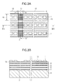
- FIG. 1A is a plan view showing composite semiconductor devices 100 according to the first embodiment of the present invention before the composite semiconductor devices 100 are divided from a semiconductor wafer.
- FIG. 1B is a sectional view taken along line IB-IB in FIG. 1A .
- the composite semiconductor device 100 includes a semiconductor substrate 3 (for example, Si substrate) and a plurality of (in this example, four) wiring layers 2 layered on the semiconductor substrate 3.
- the wiring layers 2 are composed of, at least, conductive films (i.e., wiring patterns). Insulation films 2b are formed on the wiring layers 2.
- a semiconductor thin-film layer 15 is formed on the surface of the semiconductor wafer (i.e., the substrate 3, the wiring layers 2 and the insulation films 2b).
- the semiconductor thin-film layer 15 has a plurality of semiconductor elements 1 as LED elements.
- Device-forming areas 10 are defined on the top surface of the semiconductor wafer.
- the semiconductor thin-film layer 15 with a plurality of the semiconductor elements 1 is disposed in the device-forming areas 10.
- Dicing areas 11 are defined on the top surface of the semiconductor wafer and extend in Y direction ( FIG. 1A ) between the adjacent device-forming areas 10.
- Dicing lines 12 i.e., dicing positions
- the wiring layers 2 can be composed of, for example, Al-based material such as AlSiCu, AlSi, AlNi, AlTi and AlCr, Cu or the like.
- the insulation films 2b can be composed of SiO2, SOG or the like.
- driving circuits are formed on the wiring layers 2 for driving the semiconductor elements 1.
- the semiconductor thin-film layer 15 can be composed of III-V compound semiconductor (for example, GaAs, AlGaAs or the like), III-V nitride semiconductor (for example, GaN, AlGaN of the like) or the like.
- the wiring layers 2 extend also through the dicing area 11.
- each wiring layer 2 is divided into a plurality of small sections so as to form separate pattern portion 7 which is not related to a circuit operation. Since the wiring layers 2 extend also through the dicing area 11, the difference in height between the dicing area 11 and the device-forming area 10 (due to the existence of the wiring layers 2) is reduced, and a flatness of the upper surface of the semiconductor wafer is maintained.
- the separate pattern portions 7 are formed at the same time as the formation of the wiring layers 2 that constitute driving circuits.
- the adjacent wiring layers 2 are connected to each other via connecting portions 8 in the layering direction (i.e., Z direction in FIG. 1B ) of the wiring layers 2.
- the connecting portions 8 are formed of a material such as tungsten having excellent adhesion property, high hardness and high corrosion resistance property.
- Each connecting portion 8 is disposed on the device-forming area 10 side with respect to the dicing position (i.e., the dicing line 12) defined in the dicing area 11.
- each connecting portion 8' is formed on at least an end of the device-forming area 10 so as to face the dicing area 11.
- the connecting portion 8 can be formed so as to surround the device-forming area 10.
- the uppermost wiring layer 2 is connected to the semiconductor thin-film layer 15 via a not shown material having excellent adhesion property (for example, tungsten having high hardness and high corrosion resistance property).
- the wiring layers 2 need to be connected to each other via the connecting portions 8 on at least a position between the dicing line 12 and an end 1a of the endmost semiconductor element 1 closest to the dicing line 12 ( FIG. 1A ).
- a width of each connecting portion 8 in the inward direction of the device-forming area 10 is not limited. Although one connecting portion 8 is provided on each device-forming area 10 side with respect to the dicing position (the dicing line 12) in FIG. 1A , two or more connecting portions 8 can be provided on each device-forming area 10 side with respect to the dicing position.
- a high precision dicing is performed in accordance with downsizing and upgrading of the composite semiconductor device 10.
- the dicing is performed along the dicing lines 12 defined in the dicing area 11 in the close vicinity of the device-forming areas 10 as shown in FIG. 1A .
- FIG. 2 is a sectional view for schematically illustrating a state of the semiconductor wafer in the dicing process.
- a reference numeral 6 indicates a cutting groove formed by a dicing blade.
- a reference numeral 5 indicates a tape bonded onto a backside of the semiconductor substrate 3 so as to prevent divided semiconductor chips from scattering.
- an ultraviolet-curable dicing tape is used as the tape 5.
- the connecting portions 8 prevent propagation of the crack 4 to the inside of the device-forming area 10. Due to the excellent adhesion property of the connecting portions 8, the crack 4 is prevented from reaching inside the device-forming area 10.
- FIG. 3A is a plan view showing a composite semiconductor device according to the comparison example.
- FIG. 3B is a sectional view taken along line IIIB-IIIB in FIG. 3A .
- FIG. 4 is a sectional view for schematically illustrating a state of a semiconductor wafer in the dicing process according to the comparison example.
- components that are the same as those shown in FIGS. 1A, 1B and 2 are assigned the same reference numerals.
- the separate pattern portions 7 effectively prevent propagation of the force to the device-forming area 10.
- the cracks 4 generated from the cutting groove 6 may propagate to the wiring layers 2 in the close vicinity of the cutting groove 6 as shown in FIG. 4 .
- the cracks 4 may cause separation of the wiring layers 2 and may propagate along the wiring' layer 2 to the inside of the device-forming area 10.
- the connecting portion 8 is formed on the device-forming area 10 side with respect to the dicing position, and therefore the connecting portion 8 prevents propagation of the crack 4 to the inside of the device-forming area 10 due to the excellent adhesion property of the connecting portions 8. Therefore, the crack 4 does not affect the semiconductor chip (i.e., the composite semiconductor device 100), with the result that yield ratio in the manufacturing process of the composite semiconductor device 100 can be enhanced.
- FIGS. 5A through 5F and FIGS. 6A through 6F show the manufacturing method of the composite semiconductor device 100 according to the first embodiment of the present invention.
- the semiconductor substrate 3 composed of, for example, Si is prepared.
- a conductive layer 20 (for forming the wiring layer 2) such as AlSiCu, AlSi, AlNi, AlTi and AlCr, Cu are formed on the semiconductor substrate 3.
- the conductive layer 20 is patterned using conventional photolithography, so as to form the wiring layer 2 and the separate pattern portion 7.
- the insulation film 2b is formed on the wiring layer 2 and the separate pattern portion 7 on the semiconductor substrate 3.
- holes 8H are formed through the insulation film 2b in the vicinity of the ends of the device-forming area 10 so that the holes 8H reach the surface of the wiring layer 2.
- the connecting portions 8 of tungsten or the like are formed in the holes 8H.
- FIGS. 5A through 5F are repeated so that a plurality of the wiring layers 2 and insulation films 2b are layered as shown in FIG. 1B .
- the semiconductor wafer obtained by the processes of FIGS. 5A through 5F is expressed as a "semiconductor wafer 21" as shown in FIG. 6A .
- the detail of the semiconductor wafer 21 is omitted in FIGS. 6A through 6F .
- a semiconductor thin-film layer 22 for forming the semiconductor elements 1 (i.e., driven elements) and the semiconductor thin-film layer 15 is bonded onto the upper surface of the semiconductor wafer 21.
- the semiconductor thin-film layer 22 is composed of, for example, a compound semiconductor such as III-V compound semiconductor, for example, GaAs, AlGaAs or the like.
- the semiconductor thin-film layer 22 is patterned using a conventional photolithography so as to form a plurality of semiconductor elements 1 and the semiconductor thin-film layer 15 (omitted in FIG. 6C ) in the device-forming area 10. Further, wirings are formed for electrically connecting the semiconductor elements 1 and driving circuits (not shown).
- cutting grooves 6 are formed on the semiconductor wafer 21 at the dicing area 11 (between the semiconductor elements 1) using the dicing blade to thereby divide the semiconductor wafer 21 into a plurality of chips, so as to obtain a plurality of composite semiconductor devices 100 as was described with reference to FIGS. 1A and 1B .
- the ultraviolet curable dicing tape 5 is bonded onto the backside of the semiconductor wafer 21 to prevent the respective chips (i.e., the composite semiconductor devices 100) from scattering.
- a plurality of composite semiconductor devices 100 are bonded onto a mounting substrate 27 composed of glass epoxy substrate using a dice bond paste 28 or the like as shown in FIG. 6E , for manufacturing the LED array head.
- the composite semiconductor devices 100 are arranged on a line. With such a dice bonding process, an LED array head using the composite semiconductor devices 100 as shown in FIG. 6F is obtained.
- the connecting portion 8 (connecting the wiring layers 2) is disposed on the device-forming area 10 side with respect to the dicing position, and the connecting portion 8 having excellent adhesion property prevents the propagation of the crack 4 to the inside of the device-forming area 10. Accordingly, yield ratio in the manufacturing process of the composite semiconductor device 100 can be enhanced.
- FIG. 7 is a sectional view of a composite semiconductor device 100 according to the modification of the first embodiment of the present invention.
- ends 2a of the wiring layers 2 are arranged along an oblique cutting groove 6. Therefore, the dicing blade is prevented from directly contacting and damaging the wiring layers 2 in the device-forming area 10. Accordingly, it is possible to prevent the generation of the cracks 4 on the wiring layer 2 due to an impact of the dicing blade.
- Each of the connecting portions 8 is disposed on the device-forming area 10 side with respect to the dicing position.
- the connecting portions 8 are also arranged along the oblique cutting groove 6. Therefore, the connecting portions 8 are not affected by the dicing blade, and functions to prevent the propagation of the crack to the inside of the device-forming area 10.
- an interval between endmost LED elements (i.e., endmost semiconductor elements 1) of adjacent LED chips is often used in the high precision dicing between LED chips (the composite semiconductor devices 100), in order to make an interval between endmost LED elements (i.e., endmost semiconductor elements 1) of adjacent LED chips be the same as an interval between adjacent LED elements of the same LED chip (i.e., an interval between light emitting portions).
- FIG. 8 is a sectional view of the composite semiconductor device according to the comparison example.
- components that are the same as those shown in FIG. 7 are assigned the same reference numerals.
- the ends of the wiring layers 2 are arranged vertically (i.e., perpendicular to the surface of the semiconductor substrate 3).
- the dicing blade see, the cutting groove 6 directly contacts the wiring layers 2 in the device-forming area 10, and therefore the cracks 4 are generated on the wiring layer 2 in the device-forming area 10 due to the impact of the dicing blade.
- the dicing blade is prevented from contacting the wiring layers 2 in the device-forming area 10, and therefore the generation of the cracks 4 on the wiring layer 2 in the device-forming area 10 can be prevented.
- FIG. 9 is a sectional view showing a composite semiconductor device 100 according to the second embodiment of the present invention.
- components that are the same as those of the first embodiment are assigned the same reference numerals.
- dividing portions 9 are formed on the device-forming area 10 side with respect to the connecting portions 8.
- Each dividing portion 9 is formed so as to divide the wiring layer 2.
- the manufacturing process of the composite semiconductor device of the second embodiment is substantially the same as that of the first embodiment (see FIGS. 5A through 6F ).
- the dividing portions 9 are formed at the same time as the formation of the wiring layer 2 and the separate pattern portion 7 (see FIG. 5C ).
- the dicing is performed along the dicing line 12 (see FIG. 1A ) in the close vicinity of the device-forming area 10.
- the connecting portions 8 (having excellent adhesion property) prevent the propagation of the crack to the inside of the device-forming area 10.
- the dividing portions 9 in the vicinity of the connecting portions 8 prevent the propagation of stress (generated on the wiring layers 2 due to the external force caused by the dicing) to the inside of the device-forming area 10.
- yield rate can be further enhanced.
- FIG. 10 is a sectional view of a composite semiconductor device according to the modification of the second embodiment of the present invention.
- the oblique dicing (as described with reference to FIG. 7 ) is performed, and the ends 2a of the wiring layers 2 in the device-forming area 10 are arranged along the oblique cutting groove 6 formed by the dicing blade. Therefore, the dicing blade is prevented from directly contacting and damaging the wiring layers 2 in the device-forming area 10. Accordingly, it is possible to prevent the generation of the cracks 4 on the wiring layer 2 due to the impact of the dicing blade.
- Each connecting portion 8 is disposed on the device-forming area 10 side with respect to the dicing position, and each dividing portion 9 is disposed on the device-forming area 10 side with respect to the connecting portion 8.
- the connecting portions 8 and the dividing portions 9 are also arranged along the cutting groove 6. Therefore the connecting portions 8 and the dividing portions 9 are not affected by the dicing blade, and respectively function to prevent the propagation of crack and stress to the inside of the device-forming area 10.
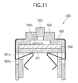
- FIG. 11 is a sectional view showing the LED head 500 according to the embodiments of the present invention.
- FIG. 12 is a plan view showing an example of an LED unit 502 of the LED head 500 shown in FIG. 11 .
- the LED head 500 includes a base 501 and an LED unit 502 mounted on the base 501.
- the LED. unit 502 includes a mounting substrate 502e (corresponding to the mounting substrate 27 as shown in FIG. 6F ) having an elongated shape, a plurality of LED arrays 502a (corresponding to the composite semiconductor devices 100 as shown in FIG. 6F ) mounted on the mounting substrate 502e.
- the LED arrays 502a include light emitting portions (corresponding to the semiconductor elements 1) linearly arranged in a longitudinal direction of the mounting substrate 502e, and driving circuits (not shown) for driving the light emitting portions.
- the mounting substrate 502e has electric components mounting areas 502b and 502c in which electric components are mounted and wirings are formed, a connector 502d for the supply of control signal and electric power from outside, or the like.
- a rod lens array 503 for focusing the lights emitted by the light emitting portions is provided above the LED array 502a.
- the rod lens array 503 is composed of a plurality of optical lenses in the form of columns arranged along the light emitting portions of the LED array 502a.
- the rod lens array 503 is held by a lens holder 504 at a position above the light emitting portions of the LED array 502a.
- the lens holder 504 is provided so as to cover the base 501 and the LED unit 502.
- the base 501, the LED unit 502 and the lens holder 504 are held by a clamper 505.
- the clamper 505 is disposed as so to penetrate through opening 501a and 502a formed on the base 501 and the lens holder 504.
- the lights emitted by the LED unit 502 irradiate a predetermined exterior member via the rod lens array 503.
- the LED head (i.e., the print head) 500 is used as, for example, an exposing device of an image forming apparatus such as an electrophotographic printer, an electrophotographic copier or the like.
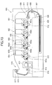
- FIG. 13 is a side view for illustrating a main part of the printer 600 as an image forming apparatus using the composite semiconductor devices according to the embodiments of the present invention.
- the printer 600 includes four process units 601, 602, 603 and 604 arranged in this order from an upstream to a downstream along a feeding path 620 of a recording medium 605.
- the process units 601, 602, 603 and 604 respectively form images of yellow, magenta, cyan and black.
- the process units 601, 602, 603 and 604 have common internal structures, and therefore the structure of the cyan process unit 603 will be described.
- the process unit 603 includes a photosensitive drum 603a as an image bearing body that is rotatable in a direction shown by arrow in FIG. 13 .
- a charging device 603b that uniformly charges the surface of the photosensitive drum 603a
- an exposing device 603c i.e., the LED head 500 shown in FIG.
- rollers and drums are respectively rotated by not a shown driving source via gears.
- a sheet cassette 606 is mounted on a lower part of the printer 600.
- the recording media 605 (such as papers) are stacked in the sheet cassette 606.
- a hopping roller 607 is disposed on the upper side of the sheet cassette 606.
- the hopping roller 607 feeds the recording medium 606 one by one out of the sheet cassette 606.
- Registration rollers 610 and 611 are disposed along the feeding path on the downstream side of the hopping roller 607.
- Pinch rollers 608 and 609 are disposed respectively facing the registration rollers 610 and 611.
- the registration rollers 610 and 611 and the pinch rollers 608 and 609 hold the recording medium 605, correct skew of the recording medium 605, and feed the recording medium 605 along the feeding path 620 toward the process units 601, 602, 603 and 604.
- the hopping roller 607 and the registration rollers 610 and 611 are respectively rotated by a not shown driving source via gears.
- Transfer rollers 612 are disposed so as to face the photosensitive drums 601a, 602a, 603a, 604a of the process units 601, 602, 603 and 604.
- the transfer rollers 612 are composed of semiconductive rubber or the like. Electric potential differences are applied between the surfaces of the photosensitive drums 601a, 602a, 603a and 604a and the surfaces of the transfer rollers 612, so as to transfer the toner images on the photosensitive drums 601a, 602a, 603a and 604a to the recording medium 605.
- a fixing device 613 includes a heat roller and a backup roller that apply heat and pressure to the toner image on the recording medium 605 to thereby fix the toner image to the recording medium 605.
- Ejection rollers 614 and 615 are disposed on the downstream side of the fixing device 613, and pinch rollers 616 and 617 are disposed respectively facing the ejection rollers 614 and 615.
- the ejection rollers 614 and 615 and the pinch rollers 616 and 617 hold the recording medium 605 and eject the recording medium 605 to a stacker portion 618.
- the ejection rollers 614 and 615 are continuously rotated by a not shown driving source via gears.
- the uppermost recording medium 605 of the stack in the sheet cassette 606 is fed out of the sheet cassette 606 by the hopping roller 607.
- the recording medium 605 is further fed by the registration rollers 610 and 611 and the pinch rollers 608 and 609 to reach a portion' between the photosensitive drum 601a of the process unit 601 and the transfer roller 612.
- the toner image formed by the exposing device 601c and developed by the developing device 601d
- the recording medium 605 is fed to the downstream side.
- the recording medium 605 further passes the process units 602, 603 and 604.
- the latent images of respective colors formed by the exposing devices 602c, 603c and 604c are developed by the developing devices 602d, 603d and 604d, and the developed toner images are respectively transferred to the recording surface of the recording medium 605 in an overlapping manner.
- the toner images of respective colors on the recording medium 605 are fixed to the recording medium 605 by the fixing device 613.
- the recording medium 605 is ejected by ejection rollers 614 and 615 and the pinch rollers 616 and 617 to the outside of the printer 600, and is placed on the stacker portion 618.
- the printer has been described as an example of the image forming apparatus.
- the present invention is also applicable to a copier, a facsimile machine, a multifunctional peripheral or the like.
- the composite semiconductor device 100 with the LED elements 1 has been described as an example of the composite semiconductor device 100.
- the composite semiconductor devices have other elements than LED elements.
Landscapes
- Physics & Mathematics (AREA)
- Optics & Photonics (AREA)
- Health & Medical Sciences (AREA)
- General Health & Medical Sciences (AREA)
- Toxicology (AREA)
- Printers Or Recording Devices Using Electromagnetic And Radiation Means (AREA)
- Dicing (AREA)
- Internal Circuitry In Semiconductor Integrated Circuit Devices (AREA)
- Led Device Packages (AREA)
- Facsimile Heads (AREA)
Abstract
Description
- The present invention relates to a composite semiconductor device such as an LED (Light Emitting Diode) array manufactured by dicing, and also relates to a print head and an image forming apparatus using the composite semiconductor device.
- The composite semiconductor devices are manufactured by forming a plurality of semiconductor elements on device-forming areas of a semiconductor wafer, and by dicing the semiconductor wafer at dicing areas (between the device-forming areas) to divide the semiconductor wafer into a plurality of semiconductor chips (i.e., composite semiconductor devices).
- Generally, a dicing blade that rotates at a high speed is used to divide the semiconductor wafer. When the semiconductor wafer is diced using the dicing blade, cracks or chipping may be generated on the semiconductor chips due to an external force applied by the dicing blade.
- In order to prevent generation of cracks and chipping on the semiconductor chips and to thereby enhance yield rate, it is proposed to provide separate pattern portions in the dicing areas of the semiconductor wafer for preventing propagation of the force to the device-forming areas in the dicing process (see, Japanese Laid-Open Patent Publication No.
2008-010571 - Recently, in accordance with downsizing and upgrading of the semiconductor devices, a high precision dicing process has been employed. In the high precision dicing process, the semiconductor wafer is diced at a position in the close vicinity of the device-forming areas. In such a case, the effect of the separate pattern portions decreases, and cracks may be generated on the semiconductor chips. Therefore, it is demanded to prevent generation of cracks on the semiconductor chips (i.e., composite semiconductor devices) even in a high precision dicing process.
- The present invention is intended to provide a composite semiconductor device capable of enhancing yield rate by preventing generation of cracks even in a high precision dicing process, and to provide a print head and an image forming apparatus using such a composite semiconductor device.
- The present invention provides a composite semiconductor device formed of a semiconductor wafer having a plurality of device-forming areas in which semiconductor elements are formed and dicing areas defined between the device-forming areas, and formed by dicing the semiconductor wafer at the dicing areas. The composite semiconductor device includes a semiconductor substrate, and a plurality of wiring layers layered on the semiconductor substrate. The wiring layers include at least conductive films. Connecting portions are formed to connect the wiring layers with each other in a layering direction of the wiring layers. Each of the connecting portions is disposed on the device-forming area side with respect to a dicing position defined in the dicing area.
- With such a configuration, even when a crack is generated on the dicing position due to an external force applied by a dicing blade, the connecting portions prevent the propagation of the crack to the inside of the device-forming area. Therefore, generation of cracks on the composite semiconductor device can be prevented, and yield rate can be enhanced.
- Further scope of applicability of the present invention will become apparent from the detailed description given hereinafter. However, it should be understood that the detailed description and specific examples, while indicating preferred embodiments of the invention, are given by way of illustration only, since various changes and modifications within the spirit and scope of the invention will become apparent to those skilled in the art from this detailed description.
- In the attached drawings:
-
FIG. 1A is a plan view showing a composite semiconductor device according to the first embodiment of the present invention; -
FIG. 1B is a sectional view taken along line IB-IB inFIG. 1A ; -
FIG. 2 is a sectional view for schematically illustrating a state of a semiconductor wafer in a dicing process according to the first embodiment of the present invention; -
FIG. 3A is a plan view showing a composite semiconductor device according to a comparison example; -
FIG. 3B is a sectional view taken along line IIIB-IIIB inFIG. 3A ; -
FIG. 4 is a sectional view for schematically illustrating a state of a semiconductor wafer in a dicing process according to the comparison example; -
FIGS. 5A through 5F are sectional views for illustrating a manufacturing process of the composite semiconductor device according to the first embodiment; -
FIGS. 6A through 6F are sectional views for illustrating the manufacturing processes of the composite semiconductor device according to the first embodiment; -
FIG. 7 is a sectional view for schematically illustrating a modification of the first embodiment of the present invention; -
FIG. 8 is a sectional view for schematically illustrating another comparison example; -
FIG. 9 is a sectional view showing a composite semiconductor device according to the second embodiment of the present invention; -
FIG. 10 is a sectional view for schematically illustrating a modification of the second embodiment of the present invention; -
FIG. 11 is a sectional view showing an LED head using the composite semiconductor device according to the embodiments of the present invention; -
FIG. 12 is a plan view showing an example of an LED unit of the LED head shown inFIG. 11 , and -
FIG. 13 schematically shows a main part of an image forming apparatus using the composite semiconductor device according to the embodiments of the present invention. - Hereinafter, embodiments of the present invention will be described with reference to the attached drawings.
-
FIG. 1A is a plan view showingcomposite semiconductor devices 100 according to the first embodiment of the present invention before thecomposite semiconductor devices 100 are divided from a semiconductor wafer.FIG. 1B is a sectional view taken along line IB-IB inFIG. 1A . - As shown in
FIGS. 1A and 1B , thecomposite semiconductor device 100 includes a semiconductor substrate 3 (for example, Si substrate) and a plurality of (in this example, four)wiring layers 2 layered on thesemiconductor substrate 3. Thewiring layers 2 are composed of, at least, conductive films (i.e., wiring patterns).Insulation films 2b are formed on thewiring layers 2. In this regard, there can be other components (not shown) than theinsulation film 2b on or besides thewiring layers 2 as necessary. - A semiconductor thin-
film layer 15 is formed on the surface of the semiconductor wafer (i.e., thesubstrate 3, thewiring layers 2 and theinsulation films 2b). The semiconductor thin-film layer 15 has a plurality ofsemiconductor elements 1 as LED elements. - Device-forming
areas 10 are defined on the top surface of the semiconductor wafer. The semiconductor thin-film layer 15 with a plurality of thesemiconductor elements 1 is disposed in the device-formingareas 10.Dicing areas 11 are defined on the top surface of the semiconductor wafer and extend in Y direction (FIG. 1A ) between the adjacent device-formingareas 10. Dicing lines 12 (i.e., dicing positions) are defined in thedicing areas 10 and extend in the Y direction in the close vicinity of the device-formingareas 10. - The wiring layers 2 can be composed of, for example, Al-based material such as AlSiCu, AlSi, AlNi, AlTi and AlCr, Cu or the like. The
insulation films 2b can be composed of SiO2, SOG or the like. Not shown driving circuits are formed on the wiring layers 2 for driving thesemiconductor elements 1. The semiconductor thin-film layer 15 can be composed of III-V compound semiconductor (for example, GaAs, AlGaAs or the like), III-V nitride semiconductor (for example, GaN, AlGaN of the like) or the like. - In this embodiment, the wiring layers 2 extend also through the dicing
area 11. In thedicing area 11, eachwiring layer 2 is divided into a plurality of small sections so as to formseparate pattern portion 7 which is not related to a circuit operation. Since the wiring layers 2 extend also through the dicingarea 11, the difference in height between the dicingarea 11 and the device-forming area 10 (due to the existence of the wiring layers 2) is reduced, and a flatness of the upper surface of the semiconductor wafer is maintained. - In this embodiment, the
separate pattern portions 7 are formed at the same time as the formation of the wiring layers 2 that constitute driving circuits. However, it is also possible to form theseparate pattern portions 7 using metal layers different from the wiring layers 2, as long as the flatness of the surface of the semiconductor wafer can be maintained. - The
adjacent wiring layers 2 are connected to each other via connectingportions 8 in the layering direction (i.e., Z direction inFIG. 1B ) of the wiring layers 2. The connectingportions 8 are formed of a material such as tungsten having excellent adhesion property, high hardness and high corrosion resistance property. Each connectingportion 8 is disposed on the device-formingarea 10 side with respect to the dicing position (i.e., the dicing line 12) defined in thedicing area 11. In this example, each connecting portion 8'is formed on at least an end of the device-formingarea 10 so as to face the dicingarea 11. For example, the connectingportion 8 can be formed so as to surround the device-formingarea 10. In this regard, theuppermost wiring layer 2 is connected to the semiconductor thin-film layer 15 via a not shown material having excellent adhesion property (for example, tungsten having high hardness and high corrosion resistance property). - The wiring layers 2 need to be connected to each other via the connecting
portions 8 on at least a position between the dicingline 12 and anend 1a of theendmost semiconductor element 1 closest to the dicing line 12 (FIG. 1A ). However, a width of each connectingportion 8 in the inward direction of the device-formingarea 10 is not limited. Although one connectingportion 8 is provided on each device-formingarea 10 side with respect to the dicing position (the dicing line 12) inFIG. 1A , two or more connectingportions 8 can be provided on each device-formingarea 10 side with respect to the dicing position. - In the manufacturing process of the
composite semiconductor device 10 having the above described configuration, a high precision dicing is performed in accordance with downsizing and upgrading of thecomposite semiconductor device 10. In the high precision dicing, the dicing is performed along the dicinglines 12 defined in thedicing area 11 in the close vicinity of the device-formingareas 10 as shown inFIG. 1A . -
FIG. 2 is a sectional view for schematically illustrating a state of the semiconductor wafer in the dicing process. Areference numeral 6 indicates a cutting groove formed by a dicing blade. Areference numeral 5 indicates a tape bonded onto a backside of thesemiconductor substrate 3 so as to prevent divided semiconductor chips from scattering. For example, an ultraviolet-curable dicing tape is used as thetape 5. - According to the first embodiment of the present invention, even when a
crack 4 is generated from the cuttinggroove 5, the connectingportions 8 prevent propagation of thecrack 4 to the inside of the device-formingarea 10. Due to the excellent adhesion property of the connectingportions 8, thecrack 4 is prevented from reaching inside the device-formingarea 10. - Here, a comparison example will be described.
FIG. 3A is a plan view showing a composite semiconductor device according to the comparison example.FIG. 3B is a sectional view taken along line IIIB-IIIB inFIG. 3A .FIG. 4 is a sectional view for schematically illustrating a state of a semiconductor wafer in the dicing process according to the comparison example. InFIGS. 3A, 3B and4 , components that are the same as those shown inFIGS. 1A, 1B and2 are assigned the same reference numerals. - In the comparison example, no connecting
portion 8 is provided between the wiring layers 2. Instead,separate pattern portion 7 is also formed on the top surface of the semiconductor wafer. - When the dicing is performed along the dicing line 12' at the center of the dicing
area 11, theseparate pattern portions 7 effectively prevent propagation of the force to the device-formingarea 10. However, when the dicing is performed along the dicingline 12 in the close vicinity of the device-formingarea 10, thecracks 4 generated from the cuttinggroove 6 may propagate to the wiring layers 2 in the close vicinity of the cuttinggroove 6 as shown inFIG. 4 . In such a case, thecracks 4 may cause separation of the wiring layers 2 and may propagate along the wiring'layer 2 to the inside of the device-formingarea 10. - In contrast, according to the first embodiment of the present invention, the connecting
portion 8 is formed on the device-formingarea 10 side with respect to the dicing position, and therefore the connectingportion 8 prevents propagation of thecrack 4 to the inside of the device-formingarea 10 due to the excellent adhesion property of the connectingportions 8. Therefore, thecrack 4 does not affect the semiconductor chip (i.e., the composite semiconductor device 100), with the result that yield ratio in the manufacturing process of thecomposite semiconductor device 100 can be enhanced. - Next, a manufacturing method of the
composite semiconductor device 100 according to the first embodiment of the present invention will be described. -
FIGS. 5A through 5F andFIGS. 6A through 6F show the manufacturing method of thecomposite semiconductor device 100 according to the first embodiment of the present invention. - First, as shown in
FIG. 5A , thesemiconductor substrate 3 composed of, for example, Si is prepared. - Next, as shown in
FIG. 5B , a conductive layer 20 (for forming the wiring layer 2) such as AlSiCu, AlSi, AlNi, AlTi and AlCr, Cu are formed on thesemiconductor substrate 3. - Then, as shown in
FIG. 5C , theconductive layer 20 is patterned using conventional photolithography, so as to form thewiring layer 2 and theseparate pattern portion 7. - Next, as shown in
FIG. 5D , theinsulation film 2b is formed on thewiring layer 2 and theseparate pattern portion 7 on thesemiconductor substrate 3. - Then, as shown in
FIG. 5E , holes 8H are formed through theinsulation film 2b in the vicinity of the ends of the device-formingarea 10 so that theholes 8H reach the surface of thewiring layer 2. - Next, as shown in
FIG. 5F , the connectingportions 8 of tungsten or the like are formed in theholes 8H. - The processes of
FIGS. 5A through 5F are repeated so that a plurality of the wiring layers 2 andinsulation films 2b are layered as shown inFIG. 1B . - The semiconductor wafer obtained by the processes of
FIGS. 5A through 5F is expressed as a "semiconductor wafer 21" as shown inFIG. 6A . The detail of thesemiconductor wafer 21 is omitted inFIGS. 6A through 6F . - Next, as shown in
FIG. 6B , a semiconductor thin-film layer 22 for forming the semiconductor elements 1 (i.e., driven elements) and the semiconductor thin-film layer 15 is bonded onto the upper surface of thesemiconductor wafer 21. The semiconductor thin-film layer 22 is composed of, for example, a compound semiconductor such as III-V compound semiconductor, for example, GaAs, AlGaAs or the like. - Then, as shown in
FIG. 6C , the semiconductor thin-film layer 22 is patterned using a conventional photolithography so as to form a plurality ofsemiconductor elements 1 and the semiconductor thin-film layer 15 (omitted inFIG. 6C ) in the device-formingarea 10. Further, wirings are formed for electrically connecting thesemiconductor elements 1 and driving circuits (not shown). - Next, as shown in
FIG. 6D , cuttinggrooves 6 are formed on thesemiconductor wafer 21 at the dicing area 11 (between the semiconductor elements 1) using the dicing blade to thereby divide thesemiconductor wafer 21 into a plurality of chips, so as to obtain a plurality ofcomposite semiconductor devices 100 as was described with reference toFIGS. 1A and 1B . - In this dicing process, the ultraviolet
curable dicing tape 5 is bonded onto the backside of thesemiconductor wafer 21 to prevent the respective chips (i.e., the composite semiconductor devices 100) from scattering. - A plurality of
composite semiconductor devices 100 are bonded onto a mountingsubstrate 27 composed of glass epoxy substrate using adice bond paste 28 or the like as shown inFIG. 6E , for manufacturing the LED array head. Thecomposite semiconductor devices 100 are arranged on a line. With such a dice bonding process, an LED array head using thecomposite semiconductor devices 100 as shown inFIG. 6F is obtained. - As described above, according to the first embodiment of the present invention, the connecting portion 8 (connecting the wiring layers 2) is disposed on the device-forming
area 10 side with respect to the dicing position, and the connectingportion 8 having excellent adhesion property prevents the propagation of thecrack 4 to the inside of the device-formingarea 10. Accordingly, yield ratio in the manufacturing process of thecomposite semiconductor device 100 can be enhanced. -
FIG. 7 is a sectional view of acomposite semiconductor device 100 according to the modification of the first embodiment of the present invention. - As shown in
FIG. 7 , there are cases where the dicing is performed at an angle with respect to a thickness direction of the semiconductor substrate 3 (i.e., the layering direction of the wiring layers 2). Such a dicing is referred to as "oblique dicing". - In this modification, ends 2a of the wiring layers 2 (in the device-forming area 10) are arranged along an
oblique cutting groove 6. Therefore, the dicing blade is prevented from directly contacting and damaging the wiring layers 2 in the device-formingarea 10. Accordingly, it is possible to prevent the generation of thecracks 4 on thewiring layer 2 due to an impact of the dicing blade. - Each of the connecting
portions 8 is disposed on the device-formingarea 10 side with respect to the dicing position. In other words, the connectingportions 8 are also arranged along theoblique cutting groove 6. Therefore, the connectingportions 8 are not affected by the dicing blade, and functions to prevent the propagation of the crack to the inside of the device-formingarea 10. - Other configurations of the modification are the same as those of the first embodiment (see
FIGS. 1A, 1B and2 ). - The above described oblique dicing is often used in the high precision dicing between LED chips (the composite semiconductor devices 100), in order to make an interval between endmost LED elements (i.e., endmost semiconductor elements 1) of adjacent LED chips be the same as an interval between adjacent LED elements of the same LED chip (i.e., an interval between light emitting portions).
- Here, a comparison example will be described.
FIG. 8 is a sectional view of the composite semiconductor device according to the comparison example. InFIG. 8 , components that are the same as those shown inFIG. 7 are assigned the same reference numerals. - In the comparison example, the ends of the wiring layers 2 are arranged vertically (i.e., perpendicular to the surface of the semiconductor substrate 3). When the oblique dicing is performed in the close vicinity of the device-forming
area 10, the dicing blade (see, the cutting groove 6) directly contacts the wiring layers 2 in the device-formingarea 10, and therefore thecracks 4 are generated on thewiring layer 2 in the device-formingarea 10 due to the impact of the dicing blade. - In contrast, according to the modification of the first embodiment of the present invention (
FIG. 7 ), the dicing blade is prevented from contacting the wiring layers 2 in the device-formingarea 10, and therefore the generation of thecracks 4 on thewiring layer 2 in the device-formingarea 10 can be prevented. -
FIG. 9 is a sectional view showing acomposite semiconductor device 100 according to the second embodiment of the present invention. InFIG. 9 , components that are the same as those of the first embodiment (shown inFIGS. 1A, 1B and2 ) are assigned the same reference numerals. - In the second embodiment of the present invention, dividing
portions 9 are formed on the device-formingarea 10 side with respect to the connectingportions 8. Each dividingportion 9 is formed so as to divide thewiring layer 2. In this regard, it is also possible to provide further dividingportions 9 on each device-formingarea 10 side with respect to the connectingportion 8. - The other configurations of the second embodiment are the same as the first embodiment.
- The manufacturing process of the composite semiconductor device of the second embodiment is substantially the same as that of the first embodiment (see
FIGS. 5A through 6F ). In this regard, the dividingportions 9 are formed at the same time as the formation of thewiring layer 2 and the separate pattern portion 7 (seeFIG. 5C ). - As was described in the first embodiment, the dicing is performed along the dicing line 12 (see
FIG. 1A ) in the close vicinity of the device-formingarea 10. Even when a crack is generated from the cuttinggroove 6 by the dicing, the connecting portions 8 (having excellent adhesion property) prevent the propagation of the crack to the inside of the device-formingarea 10. Further, the dividingportions 9 in the vicinity of the connectingportions 8 prevent the propagation of stress (generated on the wiring layers 2 due to the external force caused by the dicing) to the inside of the device-formingarea 10. - Therefore, according to the second embodiment of the present invention, yield rate can be further enhanced.
-
FIG. 10 is a sectional view of a composite semiconductor device according to the modification of the second embodiment of the present invention. - In this modification, the oblique dicing (as described with reference to
FIG. 7 ) is performed, and theends 2a of the wiring layers 2 in the device-formingarea 10 are arranged along theoblique cutting groove 6 formed by the dicing blade. Therefore, the dicing blade is prevented from directly contacting and damaging the wiring layers 2 in the device-formingarea 10. Accordingly, it is possible to prevent the generation of thecracks 4 on thewiring layer 2 due to the impact of the dicing blade. - Each connecting
portion 8 is disposed on the device-formingarea 10 side with respect to the dicing position, and each dividingportion 9 is disposed on the device-formingarea 10 side with respect to the connectingportion 8. In other words, the connectingportions 8 and the dividingportions 9 are also arranged along the cuttinggroove 6. Therefore the connectingportions 8 and the dividingportions 9 are not affected by the dicing blade, and respectively function to prevent the propagation of crack and stress to the inside of the device-formingarea 10. - Although the dicing in the Y direction (see
FIG. 1A ) has been described, the first and second embodiments and modifications thereof can be applied to the dicing in the X direction (seeFIG. 1A ). - Next, a description will be made of an LED head (i.e., a print head) 500 using the
composite semiconductor device 100 according to the first and second embodiments of the present invention with reference toFIGS. 11 and12 .FIG. 11 is a sectional view showing theLED head 500 according to the embodiments of the present invention.FIG. 12 is a plan view showing an example of anLED unit 502 of theLED head 500 shown inFIG. 11 . - As shown in
FIG. 11 , theLED head 500 includes abase 501 and anLED unit 502 mounted on thebase 501. - As shown in
FIG. 12 , the LED.unit 502 includes a mountingsubstrate 502e (corresponding to the mountingsubstrate 27 as shown inFIG. 6F ) having an elongated shape, a plurality ofLED arrays 502a (corresponding to thecomposite semiconductor devices 100 as shown inFIG. 6F ) mounted on the mountingsubstrate 502e. TheLED arrays 502a include light emitting portions (corresponding to the semiconductor elements 1) linearly arranged in a longitudinal direction of the mountingsubstrate 502e, and driving circuits (not shown) for driving the light emitting portions. In addition, the mountingsubstrate 502e has electriccomponents mounting areas connector 502d for the supply of control signal and electric power from outside, or the like. - Further, as shown in
FIG. 11 , arod lens array 503 for focusing the lights emitted by the light emitting portions is provided above theLED array 502a. Therod lens array 503 is composed of a plurality of optical lenses in the form of columns arranged along the light emitting portions of theLED array 502a. Therod lens array 503 is held by alens holder 504 at a position above the light emitting portions of theLED array 502a. - The
lens holder 504 is provided so as to cover thebase 501 and theLED unit 502. Thebase 501, theLED unit 502 and thelens holder 504 are held by aclamper 505. Theclamper 505 is disposed as so to penetrate throughopening base 501 and thelens holder 504. The lights emitted by theLED unit 502 irradiate a predetermined exterior member via therod lens array 503. The LED head (i.e., the print head) 500 is used as, for example, an exposing device of an image forming apparatus such as an electrophotographic printer, an electrophotographic copier or the like. - Next, a description will be made of an image forming apparatus using the above described exposing device (i.e., the LED head 500) with reference to
FIG. 13 . -
FIG. 13 is a side view for illustrating a main part of theprinter 600 as an image forming apparatus using the composite semiconductor devices according to the embodiments of the present invention. As shown inFIG. 13 , theprinter 600 includes fourprocess units feeding path 620 of arecording medium 605. Theprocess units process units cyan process unit 603 will be described. - The
process unit 603 includes aphotosensitive drum 603a as an image bearing body that is rotatable in a direction shown by arrow inFIG. 13 . Along the circumference of thephotosensitive drum 603a, acharging device 603b that uniformly charges the surface of thephotosensitive drum 603a, an exposingdevice 603c (i.e., theLED head 500 shown inFIG. 11 ) that selectively exposes the surface of thephotosensitive drum 603a to form a latent image, a developingdevice 603d that develops the latent image on the surface of thephotosensitive drum 603a using a toner of a predetermined color (cyan), a cleaning device that removes the residual toner from the surface of thephotosensitive drum 603a, or the like in this order along the rotational direction of thephotosensitive drum 603a. These rollers and drums are respectively rotated by not a shown driving source via gears. - A
sheet cassette 606 is mounted on a lower part of theprinter 600. The recording media 605 (such as papers) are stacked in thesheet cassette 606. A hoppingroller 607 is disposed on the upper side of thesheet cassette 606. The hoppingroller 607 feeds therecording medium 606 one by one out of thesheet cassette 606.Registration rollers roller 607.Pinch rollers registration rollers registration rollers pinch rollers recording medium 605, correct skew of therecording medium 605, and feed therecording medium 605 along thefeeding path 620 toward theprocess units roller 607 and theregistration rollers -
Transfer rollers 612 are disposed so as to face thephotosensitive drums process units transfer rollers 612 are composed of semiconductive rubber or the like. Electric potential differences are applied between the surfaces of thephotosensitive drums transfer rollers 612, so as to transfer the toner images on thephotosensitive drums recording medium 605. - A fixing
device 613 includes a heat roller and a backup roller that apply heat and pressure to the toner image on therecording medium 605 to thereby fix the toner image to therecording medium 605.Ejection rollers device 613, and pinchrollers ejection rollers ejection rollers pinch rollers recording medium 605 and eject therecording medium 605 to astacker portion 618. Theejection rollers - Next, an operation of the
printer 600 will be described. - First, the
uppermost recording medium 605 of the stack in thesheet cassette 606 is fed out of thesheet cassette 606 by the hoppingroller 607. Therecording medium 605 is further fed by theregistration rollers pinch rollers photosensitive drum 601a of theprocess unit 601 and thetransfer roller 612. In a state where therecording medium 605 is sandwiched between thephotosensitive drum 601a and thetransfer roller 612, the toner image (formed by the exposing device 601c and developed by the developing device 601d) is transferred from thephotosensitive drum 601a to a recording surface of therecording medium 605, and therecording medium 605 is fed to the downstream side. - The
recording medium 605 further passes theprocess units devices 602c, 603c and 604c are developed by the developingdevices 602d, 603d and 604d, and the developed toner images are respectively transferred to the recording surface of therecording medium 605 in an overlapping manner. The toner images of respective colors on therecording medium 605 are fixed to therecording medium 605 by the fixingdevice 613. Thereafter, therecording medium 605 is ejected byejection rollers pinch rollers printer 600, and is placed on thestacker portion 618. - With such processes, a color image of high quality is formed on the
recording medium 605. - In the above description, the printer has been described as an example of the image forming apparatus. However, the present invention is also applicable to a copier, a facsimile machine, a multifunctional peripheral or the like.
- Further, in the above description, the
composite semiconductor device 100 with theLED elements 1 has been described as an example of thecomposite semiconductor device 100. However, it is also possible that the composite semiconductor devices have other elements than LED elements. - While the preferred embodiments of the present invention have been illustrated in detail, it should be apparent that modifications and improvements may be made to the invention without departing from the spirit and scope of the invention as described in the following claims.
Claims (5)
- A composite semiconductor device (100) formed of a semiconductor wafer (21) having a plurality of device-forming areas (10) in which semiconductor elements (1) are formed and dicing areas (11) defined between said device-forming areas (10), and formed by dicing said semiconductor wafer (21) at said dicing areas (11),
said composite semiconductor device (100) comprising:a semiconductor substrate (3), anda plurality of wiring layers (2) layered on said semiconductor substrate (3), said wiring layers (2) including at least conductive films,wherein connecting portions (8) are formed to connect said wiring layers (2) with each other in a layering direction of said wiring layers (2), each of said connecting portions (8) being disposed on said device-forming area (10) side with respect to a dicing position (12) defined in said dicing area (11). - The composite semiconductor device (100) according to claim 1, wherein said wiring layer (2) has a dividing portion (9) on said device-forming area (10) side with respect to said connecting portion (8).
- The composite semiconductor device (100) according to claim 1 or 2, wherein ends (2a) of said wiring layers (2) are arranged in accordance with an angle at which said semiconductor wafer is diced, each of said ends (2a) being disposed on said device-forming area (10) side with respect to said dicing position (12).
- A print head (500) comprising:a mounting substrate (502e) on which a plurality of said composite semiconductor devices (502a) according to any one of claims 1 to 3 are linearly arranged;a lens array (503) disposed so as to face said composite semiconductor devices (502a), said lens array being configured to focus lights emitted by said semiconductor elements (1) of said composite semiconductor devices (502a).
- An image forming apparatus (600) comprising:said print head (500) according to claim 4, andan image bearing body (601a, 602a, 603a, 604a) having a surface exposed by said print head (500) so as to form a latent image on said surface.
Applications Claiming Priority (1)
| Application Number | Priority Date | Filing Date | Title |
|---|---|---|---|
| JP2008171008A JP2010010595A (en) | 2008-06-30 | 2008-06-30 | Composite semiconductor device, print head, and image forming apparatus |
Publications (3)
| Publication Number | Publication Date |
|---|---|
| EP2141022A2 true EP2141022A2 (en) | 2010-01-06 |
| EP2141022A3 EP2141022A3 (en) | 2012-08-08 |
| EP2141022B1 EP2141022B1 (en) | 2014-03-26 |
Family
ID=41128558
Family Applications (1)
| Application Number | Title | Priority Date | Filing Date |
|---|---|---|---|
| EP09161214.3A Active EP2141022B1 (en) | 2008-06-30 | 2009-05-27 | Composite semiconductor device, print head and image forming apparatus |
Country Status (4)
| Country | Link |
|---|---|
| US (1) | US8130253B2 (en) |
| EP (1) | EP2141022B1 (en) |
| JP (1) | JP2010010595A (en) |
| CN (1) | CN101621048B (en) |
Families Citing this family (4)
| Publication number | Priority date | Publication date | Assignee | Title |
|---|---|---|---|---|
| JP2017055014A (en) * | 2015-09-11 | 2017-03-16 | 株式会社東芝 | Manufacturing method of semiconductor device |
| KR102646901B1 (en) | 2016-12-23 | 2024-03-12 | 삼성전자주식회사 | Image sensor and method of manufacturing the same |
| TWI664747B (en) * | 2017-03-27 | 2019-07-01 | PlayNitride Inc. | Patterned substrate and light emitting diode wafer |
| JP7027234B2 (en) * | 2018-04-16 | 2022-03-01 | 株式会社ディスコ | Wafer processing method |
Citations (4)
| Publication number | Priority date | Publication date | Assignee | Title |
|---|---|---|---|---|
| US6521975B1 (en) | 1999-05-20 | 2003-02-18 | Texas Instruments Incorporated | Scribe street seals in semiconductor devices and method of fabrication |
| JP2006332344A (en) | 2005-05-26 | 2006-12-07 | Matsushita Electric Ind Co Ltd | Semiconductor device |
| JP2008010571A (en) | 2006-06-28 | 2008-01-17 | Oki Data Corp | Semiconductor device, LED head, and image forming apparatus |
| JP2008066716A (en) | 2006-08-10 | 2008-03-21 | Matsushita Electric Ind Co Ltd | Semiconductor device |
Family Cites Families (4)
| Publication number | Priority date | Publication date | Assignee | Title |
|---|---|---|---|---|
| JP2000195827A (en) * | 1998-12-25 | 2000-07-14 | Oki Electric Ind Co Ltd | LED array chip, method of manufacturing the same, and dicing apparatus |
| CN100524680C (en) * | 2005-11-24 | 2009-08-05 | 株式会社理光 | Semiconductor wafer including semiconductor chips divided by scribe lines and process-monitoring electrode pads formed on the scribe lines |
| JP4931422B2 (en) * | 2006-01-13 | 2012-05-16 | 株式会社リコー | Semiconductor wafer |
| KR100881109B1 (en) * | 2005-11-24 | 2009-02-02 | 가부시키가이샤 리코 | A semiconductor wafer comprising a semiconductor chip divided by a scribe line and a process-monitor electrode pad formed on the scribe line |
-
2008
- 2008-06-30 JP JP2008171008A patent/JP2010010595A/en active Pending
-
2009
- 2009-05-27 CN CN200910145514.5A patent/CN101621048B/en active Active
- 2009-05-27 EP EP09161214.3A patent/EP2141022B1/en active Active
- 2009-05-29 US US12/457,019 patent/US8130253B2/en active Active
Patent Citations (4)
| Publication number | Priority date | Publication date | Assignee | Title |
|---|---|---|---|---|
| US6521975B1 (en) | 1999-05-20 | 2003-02-18 | Texas Instruments Incorporated | Scribe street seals in semiconductor devices and method of fabrication |
| JP2006332344A (en) | 2005-05-26 | 2006-12-07 | Matsushita Electric Ind Co Ltd | Semiconductor device |
| JP2008010571A (en) | 2006-06-28 | 2008-01-17 | Oki Data Corp | Semiconductor device, LED head, and image forming apparatus |
| JP2008066716A (en) | 2006-08-10 | 2008-03-21 | Matsushita Electric Ind Co Ltd | Semiconductor device |
Also Published As
| Publication number | Publication date |
|---|---|
| EP2141022B1 (en) | 2014-03-26 |
| JP2010010595A (en) | 2010-01-14 |
| CN101621048B (en) | 2014-07-30 |
| CN101621048A (en) | 2010-01-06 |
| US20090322852A1 (en) | 2009-12-31 |
| US8130253B2 (en) | 2012-03-06 |
| EP2141022A3 (en) | 2012-08-08 |
Similar Documents
| Publication | Publication Date | Title |
|---|---|---|
| CN101064330B (en) | Composite semiconductor light emitting device, led head , and image forming apparatus | |
| US8343848B2 (en) | Semiconductor device, LED print head and image-forming apparatus using same, and method of manufacturing semiconductor device | |
| US20080023716A1 (en) | Semiconductor combined device, light emitting diode head, and image forming apparatus | |
| CN101047174B (en) | Composite semiconductor device, LED head, and image forming apparatus | |
| EP1873825A2 (en) | Semiconductor device, LED head and image forming apparatus | |
| US7893455B2 (en) | Semiconductor light emitting device with stress absorber, LED printhead, and image forming apparatus | |
| US9429867B2 (en) | Semiconductor apparatus, exposing head, and image forming apparatus | |
| JP6508977B2 (en) | Semiconductor device, LED head, and image forming apparatus | |
| US7541620B2 (en) | Semiconductor device, light emitting diode print head, and image forming apparatus | |
| JP2009212394A (en) | Semiconductor device, led head, and image forming apparatus | |
| EP2141022B1 (en) | Composite semiconductor device, print head and image forming apparatus | |
| JP4601464B2 (en) | Semiconductor device, print head, and image forming apparatus using the same | |
| JP2009238893A (en) | Semiconductor device, optical print head, and image forming apparatus | |
| JP6950484B2 (en) | Semiconductor elements, light emitting substrates, optical print heads, image forming devices | |
| JP2016192513A (en) | Semiconductor device, semiconductor element array device, and image forming apparatus | |
| US9614125B2 (en) | Composite element chip, a semiconductor device and manufacturing method thereof, a printing head, and an image forming apparatus | |
| JP6296902B2 (en) | Semiconductor device, image forming apparatus using the semiconductor device, and image reading apparatus | |
| JP2009147352A (en) | Semiconductor device, LED head, and image forming apparatus | |
| JP2008166611A (en) | Light emitting element array, optical print head and image forming apparatus using the same | |
| JP5546315B2 (en) | Electronic device, optical print head, and image forming apparatus | |
| JP2021163941A (en) | Light-emitting element chip, led head and image formation apparatus | |
| JP2010003890A (en) | Compound semiconductor device, print head, and image forming apparatus |
Legal Events
| Date | Code | Title | Description |
|---|---|---|---|
| PUAI | Public reference made under article 153(3) epc to a published international application that has entered the european phase |
Free format text: ORIGINAL CODE: 0009012 |
|
| AK | Designated contracting states |
Kind code of ref document: A2 Designated state(s): AT BE BG CH CY CZ DE DK EE ES FI FR GB GR HR HU IE IS IT LI LT LU LV MC MK MT NL NO PL PT RO SE SI SK TR |
|
| PUAL | Search report despatched |
Free format text: ORIGINAL CODE: 0009013 |
|
| AK | Designated contracting states |
Kind code of ref document: A3 Designated state(s): AT BE BG CH CY CZ DE DK EE ES FI FR GB GR HR HU IE IS IT LI LT LU LV MC MK MT NL NO PL PT RO SE SI SK TR |
|
| RIC1 | Information provided on ipc code assigned before grant |
Ipc: H01L 27/15 20060101ALI20120704BHEP Ipc: H01L 21/78 20060101ALI20120704BHEP Ipc: B41J 2/45 20060101AFI20120704BHEP |
|
| 17P | Request for examination filed |
Effective date: 20130205 |
|
| GRAP | Despatch of communication of intention to grant a patent |
Free format text: ORIGINAL CODE: EPIDOSNIGR1 |
|
| INTG | Intention to grant announced |
Effective date: 20131021 |
|
| GRAS | Grant fee paid |
Free format text: ORIGINAL CODE: EPIDOSNIGR3 |
|
| GRAA | (expected) grant |
Free format text: ORIGINAL CODE: 0009210 |
|
| AK | Designated contracting states |
Kind code of ref document: B1 Designated state(s): AT BE BG CH CY CZ DE DK EE ES FI FR GB GR HR HU IE IS IT LI LT LU LV MC MK MT NL NO PL PT RO SE SI SK TR |
|
| REG | Reference to a national code |
Ref country code: GB Ref legal event code: FG4D |
|
| REG | Reference to a national code |
Ref country code: CH Ref legal event code: EP |
|
| REG | Reference to a national code |
Ref country code: AT Ref legal event code: REF Ref document number: 658754 Country of ref document: AT Kind code of ref document: T Effective date: 20140415 |
|
| REG | Reference to a national code |
Ref country code: IE Ref legal event code: FG4D |
|
| REG | Reference to a national code |
Ref country code: DE Ref legal event code: R096 Ref document number: 602009022711 Country of ref document: DE Effective date: 20140508 |
|
| REG | Reference to a national code |
Ref country code: NL Ref legal event code: T3 |
|
| PG25 | Lapsed in a contracting state [announced via postgrant information from national office to epo] |
Ref country code: NO Free format text: LAPSE BECAUSE OF FAILURE TO SUBMIT A TRANSLATION OF THE DESCRIPTION OR TO PAY THE FEE WITHIN THE PRESCRIBED TIME-LIMIT Effective date: 20140626 Ref country code: LT Free format text: LAPSE BECAUSE OF FAILURE TO SUBMIT A TRANSLATION OF THE DESCRIPTION OR TO PAY THE FEE WITHIN THE PRESCRIBED TIME-LIMIT Effective date: 20140326 |
|
| REG | Reference to a national code |
Ref country code: AT Ref legal event code: MK05 Ref document number: 658754 Country of ref document: AT Kind code of ref document: T Effective date: 20140326 |
|
| REG | Reference to a national code |
Ref country code: LT Ref legal event code: MG4D |
|
| PG25 | Lapsed in a contracting state [announced via postgrant information from national office to epo] |
Ref country code: FI Free format text: LAPSE BECAUSE OF FAILURE TO SUBMIT A TRANSLATION OF THE DESCRIPTION OR TO PAY THE FEE WITHIN THE PRESCRIBED TIME-LIMIT Effective date: 20140326 Ref country code: SE Free format text: LAPSE BECAUSE OF FAILURE TO SUBMIT A TRANSLATION OF THE DESCRIPTION OR TO PAY THE FEE WITHIN THE PRESCRIBED TIME-LIMIT Effective date: 20140326 |
|
| PG25 | Lapsed in a contracting state [announced via postgrant information from national office to epo] |
Ref country code: HR Free format text: LAPSE BECAUSE OF FAILURE TO SUBMIT A TRANSLATION OF THE DESCRIPTION OR TO PAY THE FEE WITHIN THE PRESCRIBED TIME-LIMIT Effective date: 20140326 Ref country code: LV Free format text: LAPSE BECAUSE OF FAILURE TO SUBMIT A TRANSLATION OF THE DESCRIPTION OR TO PAY THE FEE WITHIN THE PRESCRIBED TIME-LIMIT Effective date: 20140326 |
|
| PG25 | Lapsed in a contracting state [announced via postgrant information from national office to epo] |
Ref country code: EE Free format text: LAPSE BECAUSE OF FAILURE TO SUBMIT A TRANSLATION OF THE DESCRIPTION OR TO PAY THE FEE WITHIN THE PRESCRIBED TIME-LIMIT Effective date: 20140326 Ref country code: BE Free format text: LAPSE BECAUSE OF FAILURE TO SUBMIT A TRANSLATION OF THE DESCRIPTION OR TO PAY THE FEE WITHIN THE PRESCRIBED TIME-LIMIT Effective date: 20140326 Ref country code: CY Free format text: LAPSE BECAUSE OF FAILURE TO SUBMIT A TRANSLATION OF THE DESCRIPTION OR TO PAY THE FEE WITHIN THE PRESCRIBED TIME-LIMIT Effective date: 20140326 Ref country code: CZ Free format text: LAPSE BECAUSE OF FAILURE TO SUBMIT A TRANSLATION OF THE DESCRIPTION OR TO PAY THE FEE WITHIN THE PRESCRIBED TIME-LIMIT Effective date: 20140326 Ref country code: IS Free format text: LAPSE BECAUSE OF FAILURE TO SUBMIT A TRANSLATION OF THE DESCRIPTION OR TO PAY THE FEE WITHIN THE PRESCRIBED TIME-LIMIT Effective date: 20140726 Ref country code: BG Free format text: LAPSE BECAUSE OF FAILURE TO SUBMIT A TRANSLATION OF THE DESCRIPTION OR TO PAY THE FEE WITHIN THE PRESCRIBED TIME-LIMIT Effective date: 20140626 Ref country code: RO Free format text: LAPSE BECAUSE OF FAILURE TO SUBMIT A TRANSLATION OF THE DESCRIPTION OR TO PAY THE FEE WITHIN THE PRESCRIBED TIME-LIMIT Effective date: 20140326 |
|
| PG25 | Lapsed in a contracting state [announced via postgrant information from national office to epo] |
Ref country code: ES Free format text: LAPSE BECAUSE OF FAILURE TO SUBMIT A TRANSLATION OF THE DESCRIPTION OR TO PAY THE FEE WITHIN THE PRESCRIBED TIME-LIMIT Effective date: 20140326 Ref country code: PL Free format text: LAPSE BECAUSE OF FAILURE TO SUBMIT A TRANSLATION OF THE DESCRIPTION OR TO PAY THE FEE WITHIN THE PRESCRIBED TIME-LIMIT Effective date: 20140326 Ref country code: SK Free format text: LAPSE BECAUSE OF FAILURE TO SUBMIT A TRANSLATION OF THE DESCRIPTION OR TO PAY THE FEE WITHIN THE PRESCRIBED TIME-LIMIT Effective date: 20140326 Ref country code: AT Free format text: LAPSE BECAUSE OF FAILURE TO SUBMIT A TRANSLATION OF THE DESCRIPTION OR TO PAY THE FEE WITHIN THE PRESCRIBED TIME-LIMIT Effective date: 20140326 |
|
| PG25 | Lapsed in a contracting state [announced via postgrant information from national office to epo] |
Ref country code: LU Free format text: LAPSE BECAUSE OF FAILURE TO SUBMIT A TRANSLATION OF THE DESCRIPTION OR TO PAY THE FEE WITHIN THE PRESCRIBED TIME-LIMIT Effective date: 20140527 Ref country code: PT Free format text: LAPSE BECAUSE OF FAILURE TO SUBMIT A TRANSLATION OF THE DESCRIPTION OR TO PAY THE FEE WITHIN THE PRESCRIBED TIME-LIMIT Effective date: 20140728 |
|
| REG | Reference to a national code |
Ref country code: CH Ref legal event code: PL |
|
| REG | Reference to a national code |
Ref country code: DE Ref legal event code: R097 Ref document number: 602009022711 Country of ref document: DE |
|
| PG25 | Lapsed in a contracting state [announced via postgrant information from national office to epo] |
Ref country code: MC Free format text: LAPSE BECAUSE OF FAILURE TO SUBMIT A TRANSLATION OF THE DESCRIPTION OR TO PAY THE FEE WITHIN THE PRESCRIBED TIME-LIMIT Effective date: 20140326 Ref country code: LI Free format text: LAPSE BECAUSE OF NON-PAYMENT OF DUE FEES Effective date: 20140531 Ref country code: DK Free format text: LAPSE BECAUSE OF FAILURE TO SUBMIT A TRANSLATION OF THE DESCRIPTION OR TO PAY THE FEE WITHIN THE PRESCRIBED TIME-LIMIT Effective date: 20140326 Ref country code: CH Free format text: LAPSE BECAUSE OF NON-PAYMENT OF DUE FEES Effective date: 20140531 |
|
| PLBE | No opposition filed within time limit |
Free format text: ORIGINAL CODE: 0009261 |
|
| STAA | Information on the status of an ep patent application or granted ep patent |
Free format text: STATUS: NO OPPOSITION FILED WITHIN TIME LIMIT |
|
| REG | Reference to a national code |
Ref country code: IE Ref legal event code: MM4A |
|
| 26N | No opposition filed |
Effective date: 20150106 |
|
| PG25 | Lapsed in a contracting state [announced via postgrant information from national office to epo] |
Ref country code: IT Free format text: LAPSE BECAUSE OF FAILURE TO SUBMIT A TRANSLATION OF THE DESCRIPTION OR TO PAY THE FEE WITHIN THE PRESCRIBED TIME-LIMIT Effective date: 20140326 |
|
| REG | Reference to a national code |
Ref country code: DE Ref legal event code: R097 Ref document number: 602009022711 Country of ref document: DE Effective date: 20150106 |
|
| PG25 | Lapsed in a contracting state [announced via postgrant information from national office to epo] |
Ref country code: IE Free format text: LAPSE BECAUSE OF NON-PAYMENT OF DUE FEES Effective date: 20140527 |
|
| PG25 | Lapsed in a contracting state [announced via postgrant information from national office to epo] |
Ref country code: SI Free format text: LAPSE BECAUSE OF FAILURE TO SUBMIT A TRANSLATION OF THE DESCRIPTION OR TO PAY THE FEE WITHIN THE PRESCRIBED TIME-LIMIT Effective date: 20140326 |
|
| PG25 | Lapsed in a contracting state [announced via postgrant information from national office to epo] |
Ref country code: MT Free format text: LAPSE BECAUSE OF FAILURE TO SUBMIT A TRANSLATION OF THE DESCRIPTION OR TO PAY THE FEE WITHIN THE PRESCRIBED TIME-LIMIT Effective date: 20140326 |
|
| REG | Reference to a national code |
Ref country code: FR Ref legal event code: PLFP Year of fee payment: 8 |
|
| PG25 | Lapsed in a contracting state [announced via postgrant information from national office to epo] |
Ref country code: GR Free format text: LAPSE BECAUSE OF FAILURE TO SUBMIT A TRANSLATION OF THE DESCRIPTION OR TO PAY THE FEE WITHIN THE PRESCRIBED TIME-LIMIT Effective date: 20140627 |
|
| PG25 | Lapsed in a contracting state [announced via postgrant information from national office to epo] |
Ref country code: HU Free format text: LAPSE BECAUSE OF FAILURE TO SUBMIT A TRANSLATION OF THE DESCRIPTION OR TO PAY THE FEE WITHIN THE PRESCRIBED TIME-LIMIT; INVALID AB INITIO Effective date: 20090527 Ref country code: TR Free format text: LAPSE BECAUSE OF FAILURE TO SUBMIT A TRANSLATION OF THE DESCRIPTION OR TO PAY THE FEE WITHIN THE PRESCRIBED TIME-LIMIT Effective date: 20140326 |
|
| REG | Reference to a national code |
Ref country code: FR Ref legal event code: PLFP Year of fee payment: 9 |
|
| REG | Reference to a national code |
Ref country code: FR Ref legal event code: PLFP Year of fee payment: 10 |
|
| PG25 | Lapsed in a contracting state [announced via postgrant information from national office to epo] |
Ref country code: MK Free format text: LAPSE BECAUSE OF FAILURE TO SUBMIT A TRANSLATION OF THE DESCRIPTION OR TO PAY THE FEE WITHIN THE PRESCRIBED TIME-LIMIT Effective date: 20140326 |
|
| REG | Reference to a national code |
Ref country code: DE Ref legal event code: R081 Ref document number: 602009022711 Country of ref document: DE Owner name: OKI ELECTRIC INDUSTRY CO., LTD., JP Free format text: FORMER OWNER: OKI DATA CORP., TOKIO/TOKYO, JP |
|
| REG | Reference to a national code |
Ref country code: GB Ref legal event code: 732E Free format text: REGISTERED BETWEEN 20220317 AND 20220323 |
|
| REG | Reference to a national code |
Ref country code: NL Ref legal event code: PD Owner name: OKI ELECTRIC INDUSTRY CO., LTD.; JP Free format text: DETAILS ASSIGNMENT: CHANGE OF OWNER(S), MERGE; FORMER OWNER NAME: OKI DATA CORPORATION Effective date: 20220308 |
|
| REG | Reference to a national code |
Ref country code: FR Ref legal event code: PLFP Year of fee payment: 15 |
|
| PGFP | Annual fee paid to national office [announced via postgrant information from national office to epo] |
Ref country code: NL Payment date: 20250409 Year of fee payment: 17 |
|
| PGFP | Annual fee paid to national office [announced via postgrant information from national office to epo] |
Ref country code: DE Payment date: 20250402 Year of fee payment: 17 |
|
| PGFP | Annual fee paid to national office [announced via postgrant information from national office to epo] |
Ref country code: GB Payment date: 20250401 Year of fee payment: 17 |
|
| PGFP | Annual fee paid to national office [announced via postgrant information from national office to epo] |
Ref country code: FR Payment date: 20250401 Year of fee payment: 17 |