EP2140408B1 - Vorrichtung und verfahren zur quantenberechnung mit qubit-arrays verschränkter zustände anhand linsen mit negativem brechnungsindex - Google Patents
Vorrichtung und verfahren zur quantenberechnung mit qubit-arrays verschränkter zustände anhand linsen mit negativem brechnungsindex Download PDFInfo
- Publication number
- EP2140408B1 EP2140408B1 EP08744366.9A EP08744366A EP2140408B1 EP 2140408 B1 EP2140408 B1 EP 2140408B1 EP 08744366 A EP08744366 A EP 08744366A EP 2140408 B1 EP2140408 B1 EP 2140408B1
- Authority
- EP
- European Patent Office
- Prior art keywords
- atoms
- negative index
- quantum computing
- computing system
- pair
- Prior art date
- Legal status (The legal status is an assumption and is not a legal conclusion. Google has not performed a legal analysis and makes no representation as to the accuracy of the status listed.)
- Active
Links
Images



Classifications
-
- G—PHYSICS
- G02—OPTICS
- G02B—OPTICAL ELEMENTS, SYSTEMS OR APPARATUS
- G02B1/00—Optical elements characterised by the material of which they are made; Optical coatings for optical elements
- G02B1/002—Optical elements characterised by the material of which they are made; Optical coatings for optical elements made of materials engineered to provide properties not available in nature, e.g. metamaterials
- G02B1/007—Optical elements characterised by the material of which they are made; Optical coatings for optical elements made of materials engineered to provide properties not available in nature, e.g. metamaterials made of negative effective refractive index materials
-
- B—PERFORMING OPERATIONS; TRANSPORTING
- B82—NANOTECHNOLOGY
- B82Y—SPECIFIC USES OR APPLICATIONS OF NANOSTRUCTURES; MEASUREMENT OR ANALYSIS OF NANOSTRUCTURES; MANUFACTURE OR TREATMENT OF NANOSTRUCTURES
- B82Y10/00—Nanotechnology for information processing, storage or transmission, e.g. quantum computing or single electron logic
-
- B—PERFORMING OPERATIONS; TRANSPORTING
- B82—NANOTECHNOLOGY
- B82Y—SPECIFIC USES OR APPLICATIONS OF NANOSTRUCTURES; MEASUREMENT OR ANALYSIS OF NANOSTRUCTURES; MANUFACTURE OR TREATMENT OF NANOSTRUCTURES
- B82Y20/00—Nanooptics, e.g. quantum optics or photonic crystals
-
- G—PHYSICS
- G06—COMPUTING OR CALCULATING; COUNTING
- G06N—COMPUTING ARRANGEMENTS BASED ON SPECIFIC COMPUTATIONAL MODELS
- G06N10/00—Quantum computing, i.e. information processing based on quantum-mechanical phenomena
- G06N10/40—Physical realisations or architectures of quantum processors or components for manipulating qubits, e.g. qubit coupling or qubit control
-
- Y—GENERAL TAGGING OF NEW TECHNOLOGICAL DEVELOPMENTS; GENERAL TAGGING OF CROSS-SECTIONAL TECHNOLOGIES SPANNING OVER SEVERAL SECTIONS OF THE IPC; TECHNICAL SUBJECTS COVERED BY FORMER USPC CROSS-REFERENCE ART COLLECTIONS [XRACs] AND DIGESTS
- Y10—TECHNICAL SUBJECTS COVERED BY FORMER USPC
- Y10S—TECHNICAL SUBJECTS COVERED BY FORMER USPC CROSS-REFERENCE ART COLLECTIONS [XRACs] AND DIGESTS
- Y10S977/00—Nanotechnology
- Y10S977/902—Specified use of nanostructure
- Y10S977/932—Specified use of nanostructure for electronic or optoelectronic application
- Y10S977/933—Spintronics or quantum computing
Definitions
- the present invention relates generally to the field of quantum computing, and more particularly, to a quantum computing device and method including qubit arrays of entangled atomic states using negative refractive index lenses.
- a three-dimensional architecture is provided.
- Quantum information processing covers a variety of fields where quantum mechanical effects are used to process information in applications such as computation and communications.
- Quantum computation involves manipulation of data in the form of quantum bits or "qubits.”
- quantum bits In contrast to classical computation, where a bit of information is used to represent only one of two possible logic states, namely a "1" or a "0,” in quantum computation, a qubit can represent both logical states simultaneously as a superposition of quantum states. This property gives rise to powerful computational parallelism. Algorithms that exploit this parallelism have been developed, e.g., for efficiently factorizing large composite integers.
- a generally recognized problem is that quantum computation, and indeed any system involving sensitive information processing, requires a quiet electromagnetic environment to operate. If the system interacts with the environment, it may lose coherence and quantum parallelism may be destroyed.
- a quantum computing system includes qubits that can be controlled and entangled with minimum interaction with external sources.
- the quantum computing system includes qubits that include at least a pair of atoms and a negative index lens disposed between the pair of atoms. Negative index metamaterials and perfect lenses may be used to provide entanglement in neutral atoms.
- One aspect of the disclosed technology relates to a quantum computing system comprising a plurality of qubits.
- Each qubit includes a pair of atoms and a negative index lens disposed between the pair of atoms.
- the quantum computing system further comprises: control circuitry operatively connected to the negative index lenses, the control circuitry being operable to switch the negative index lenses between a negative index state and a positive index state; atomic state reading circuitry configured to determine atomic spin states of the atoms; and an excitation source configured to excite the atoms.
- the negative index lens is arranged to entangle states of the pair of atoms.
- each qubit further includes a second negative index lens disposed adjacent to one of the pair of atoms and a third atom disposed adjacent to the second negative index lens.
- a qubit array includes a plurality of qubits.
- the plurality of qubits is arranged in a two-dimensional architecture.
- the plurality of qubits is arranged in a three-dimensional architecture.
- Another aspect of the disclosed technology relates to a quantum computing method that includes disposing pairs of neutral atoms on opposite sides of negative index lenses, selectively exciting the atoms using an excitation source, selectively energizing and de-energizing the negative index lenses using control circuitry operatively connected to said negative index lenses, the selectively energizing and de-energizing causing the negative index lenses to switch between a positive index state and a negative index state respectively, thereby facilitating entanglement of states of the atoms, and determining the state of at least one of the neutral atoms using atomic state reading circuitry.
- control circuitry is operatively coupled to the excitation source, and the control circuitry and the excitation source cooperate to entangle the qubits.
- One aspect of the disclosed technology includes a quantum computing device having quantum bits (“qubits”) that can be controlled and entangled with minimum interaction with external sources.
- the quantum computing device makes use of a negative index material ("NIM”) to construct a negative index lens.
- NIM negative index material
- the negative index lens is disposed between pairs of neutral atoms to provide entanglement or otherwise controllably couple the neutral atom qubits.
- FIG. 1 illustrates an example of a suitable computing system environment 10 (also referred to as a quantum computing system, a quantum computing device or a quantum computer) in which aspects of the disclosed technology may be implemented.
- the computing system environment 10 is only one example of a suitable computing environment and is not intended to suggest any limitation as to the scope of use or functionality of the disclosed technology. Neither should the computing environment 10 be interpreted as having any dependency or requirement relating to any one or combination of components illustrated in the exemplary operating environment 10.
- aspects of the invention are operational with numerous other general purpose or special purpose computing system environments or configurations.
- Examples of such computing systems, environments, and/or configurations that may be suitable for use with aspects of the invention include, but are not limited to, personal computers, server computers, hand held or laptop devices, multiprocessor systems, microprocessor-based systems, set top boxes, programmable consumer electronics, network PCs, minicomputers, mainframe computers, distributed computing environments that include any suitable system component or device, and the like.
- an exemplary system for implementing aspects of the invention includes a general purpose computing device in the form of a computer 10.
- Components of the computer may include, but are not limited to, a processing unit, e.g., a quantum processing unit 12, a system memory, e.g., a general or conventional system memory 14 and/or a quantum memory 16, and a system bus 18 that couples the various system components, including the system memory (or memories), to the processing unit 12.
- the system bus 18 may be any of several types of bus structures including a memory bus or memory controller, a peripheral bus and a local bus using any of a variety of bus architectures.
- conventional memory 14 may be representative of the overall hierarchy of memory devices containing software and data used to implement the functionality of the computer 10.
- the memory may include, for example, RAM or other volatile solid-state memory, and/or other nonvolatile solid-state memory, a magnetic storage medium such as a hard disc drive, a removable storage medium or other suitable storage media.
- the memory 14 may store drivers 20, e.g., I/O device drivers, application programs 22, an operating system 24 and application program data 26.
- user input interface(s) 30 may couple a variety of user input devices 32, e.g., a mouse, a keyboard, a microphone, a gamepad or the like, to the processing unit 12 via the bus 18.
- a display such as a monitor 34 or other suitable display device may be connected to the system bus 18 via an interface, such as a video interface.
- the computer may also include other peripheral output devices, which may be connected through an output peripheral interface 38.
- the computer 10 may operate in a network environment using logical connections to one or more remote computers, e.g., personal computers, servers, routers, network PCs, peer devices or other common network nodes.
- remote computers e.g., personal computers, servers, routers, network PCs, peer devices or other common network nodes.
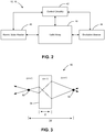
- the qubit array 40 may be operatively coupled to suitable control circuitry 42 that cooperates with or otherwise controls, one or more excitation sources 44, e.g., laser sources or sources of electric or magnetic fields, and one or more atomic state readers 46.
- excitation sources 44 e.g., laser sources or sources of electric or magnetic fields
- atomic state readers 46 e.g., atomic state readers
- the qubit array 40, control circuitry 42, excitation source 44 and atomic state reader 46 cooperate to provide physical qubits that may be entangled as well as individually addressed and set or reset for use in quantum computation processes.
- the qubit 50 includes a pair of atoms 52, e.g., neutral atoms, separated by or otherwise disposed on opposite sides of a negative index lens 54.
- a negative index lens between a pair of atoms, e.g., neutral atoms is believed to provide a physical qubit that is easily entangled, while still being individually addressed.
- the qubit (or qubit arrays) may take one of a variety of different configurations, geometries, properties or the like, without departing from the scope of the present invention.
- the negative lens is comprised of a negative index material ("NIM"), thereby being constructed as a NIM "perfect lens.”
- NIM negative index material
- the negative index lens is depicted as having a thickness d, while the atoms 52 are depicted as being separated by a distance 2d. In this configuration, the optical path length between the atoms is zero.
- the left atom's (e.g., atom A's) wave function e.g., spin down
- the right atom's (e.g., atom B's) wave function e.g., spin up
- the distance between the two focal points of the negative index lens is d(1 - n), where n is the refractive index of the negative index lens.
- n is the refractive index of the negative index lens.
- the thickness d of the negative index lens will depend on a variety of factors, including, the negative index material from which the negative index lens is constructed, e.g., the index of refraction associated with the given negative index material, the types of atoms used in the qubit and the like.
- the negative index lens 52 is constructed from a suitable negative index material, e.g., a metamaterial.
- a suitable negative index material e.g., a metamaterial.
- metamaterials are understood to include materials or objects that gain (electromagnetic) material properties from their structure rather than inheriting then directly from the material of which it is composed. Metamaterials often are associated with material properties not found in naturally-formed substances.
- the qubit 50 will include or otherwise make use of neutral cesium (Cs) atoms.
- Cs cesium
- One advantage associated with the use of Cesium atoms stems from the fact that the Cs atom has a pair of states that are separated by a transition energy equivalent to a 9.2 GHz (GigaHertz) photon.
- each qubit may include or otherwise make use of other atoms, e.g., other neutral atoms, alkaline atoms, exotic atoms and the like.
- suitable atoms include hydrogen, rubidium and positronium.
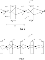
- the qubit includes a pair of negative index lenses 54, which are disposed between or otherwise separate pairs of atoms 52 e.g., neutral atoms.
- the qubit 50 may include or otherwise make use of a variety of atoms, such as neutral atoms or neutral alkaline atoms, e.g., neutral cesium atoms.
- a given negative index lens has a thickness of d, in the case of a "perfect lens" the atoms on opposite sides of the negative index lens 54 may be spaced apart by a distance of 2d.
- FIG. 5 illustrates an exemplary qubit array 40 arranged in accordance with the principles of the disclosed technology.
- the exemplary qubit array 40 includes a plurality of negative index lenses 54, where each negative index lens separates a pair of atoms 52, e.g., neutral atoms.
- the qubit array also includes a pair of negative mirrors 56, e.g., mirrors constructed of a negative index material, thereby providing "perfect mirrors," at the ends of the array.
- negative index mirrors 56 at the ends of the array 40 provide for an optical path length of zero between the respective end atoms 52 and the respective negative index mirrors 56.
- the qubit array is believed effective in providing entangled qubits in conjunction with the capability of modifying and reading individual qubits.
- the qubit array may take on the form of a one-dimensional qubit array (illustrated, for example, in FIG. 5 ).
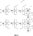
- the qubit array 40 may be extended into two dimensions.
- the qubit array is believed to be extendable into three dimensions, where the three-dimensional qubit array would be structured in a manner similar to that with respect to FIG. 6 only including a third dimension, for example a dimension having atoms and negative index lenses extending into or out of the plane on the page on which FIG. 6 is illustrated.
- excitation signals e.g., signals used to controllably modify individual qubits
- excitation sources for example, a source providing 9.2 GigaHertz (GHz) signals used to excite, for example, cesium atoms.
- the excitation signals may be provided to modify the atoms as required by a given programming algorithm using 9.2 GHz signals.
- lens control signals may be generated by an appropriate excitation source, e.g., a suitable laser source or sources together with optical fibers or arrays of mirrors to controllably direct the energy to selected negative index lenses, or a source of electric or magnetic field sources.
- an appropriate excitation source e.g., a suitable laser source or sources together with optical fibers or arrays of mirrors to controllably direct the energy to selected negative index lenses, or a source of electric or magnetic field sources.
- an appropriate excitation source e.g., a suitable laser source or sources together with optical fibers or arrays of mirrors to controllably direct the energy to selected negative index lenses, or a source of electric or magnetic field sources.
- an appropriate excitation source e.g., a suitable laser source or sources together with optical fibers or arrays of mirrors to controllably direct the energy to selected negative index lenses, or a source of electric or magnetic field sources.
- One advantageous property of the herein-discussed negative index mirrors is that the negative index mirror may be switched between negative
- FIG. 7 schematically illustrates initializing or programming the qubits using the excitation source.
- FIG. 7 illustrates energizing or otherwise activating one or more of the negative index lenses 54 to bring about a "negative index off' state, thereby transitioning the lenses 54 to a positive index material state.
- FIG. 8 illustrates the qubit array of FIG. 7 when the negative index lenses are returned to their negative index material state.
- the states of the atoms within the qubit array may be entangled.
- FIG. 8 illustrates the qubit array where the negative off mechanism has been removed along with removal of 9.2 GHz modification signals. The system can then be viewed as being isolated. At this stage, the atoms may be interrogated to determine their states.
- a quantum computing device employing the above-described qubits and qubit arrays may be operated by initializing the atoms in a set of states, selectively activating and/or deactivating the negative index lenses to initiate a type of quantum evolutionary calculation and interrogating the atoms again after a certain amount of time to obtain a result.
- FIG. 9 While for purposes of simplicity of explanation, the flow charts or functional diagram in FIG. 9 include a series of steps or functional blocks that represent one or more aspects of the quantum computing device employing the herein described qubits and/or qubit arrays, it is to be understood and appreciated that aspects of the invention described herein are not limited to the order of steps or functional blocks, as some steps or functional blocks may, in accordance with aspects of the present invention occur in different orders and/or concurrently with other steps or functional blocks from that shown or described herein. Moreover, not all illustrated steps or functional blocks representing aspects of relevant operation may be required to implement a methodology in accordance with an aspect of the invention. Furthermore, additional steps or functional blocks representative of aspects of relevant operation may be added without departing from the scope of the present invention.
- FIG. 9 an exemplary quantum computation methodology is illustrated in terms of functional blocks.
- a suitable excitation source for example, in the case of cesium atoms, a source capable of generating 9.2 GHz signals.
- the individual qubits within the qubit array may be modified as required by a suitable programming algorithm.
- the negative index lenses are activated or otherwise energized, for example, using a suitable lens control source, such as an array of lasers and mirrors positioned to controllably and selectively activate or deactivate the negative index lenses and mirrors.
- a suitable lens control source such as an array of lasers and mirrors positioned to controllably and selectively activate or deactivate the negative index lenses and mirrors.
- the negative index lenses are deactivated or otherwise returned to their negative index material properties thereby entangling the states of the qubits within the qubit array.
- the qubits or atoms within the qubit array may be probed or otherwise interrogated to determine their current state, e.g., a spin-up state, a spin-down state, or some superposition of a spin-up state and a spin-down state.
- operation of the qubit array disclosed herein includes placing the atoms within the qubit array within a set of states, e.g., in accordance with a predetermined programming algorithm, using selective activation of the negative index lenses to initiate a type of quantum evolutionary calculation, and probing or interrogating atoms within the qubit array after a certain amount of time to obtain a result.
Landscapes
- Engineering & Computer Science (AREA)
- Physics & Mathematics (AREA)
- Nanotechnology (AREA)
- Chemical & Material Sciences (AREA)
- General Physics & Mathematics (AREA)
- Theoretical Computer Science (AREA)
- Mathematical Physics (AREA)
- Crystallography & Structural Chemistry (AREA)
- Optics & Photonics (AREA)
- Data Mining & Analysis (AREA)
- Evolutionary Computation (AREA)
- Computing Systems (AREA)
- General Engineering & Computer Science (AREA)
- Mathematical Optimization (AREA)
- Software Systems (AREA)
- Mathematical Analysis (AREA)
- Pure & Applied Mathematics (AREA)
- Condensed Matter Physics & Semiconductors (AREA)
- Computational Mathematics (AREA)
- Artificial Intelligence (AREA)
- Life Sciences & Earth Sciences (AREA)
- Biophysics (AREA)
- Optical Modulation, Optical Deflection, Nonlinear Optics, Optical Demodulation, Optical Logic Elements (AREA)
Claims (13)
- System zur Quantenberechnung (10), aufweisend:mehrere Qubits (40), wobei jedes Qubit (50) aufweist:ein Paar von Atomen (52); undeine Linse mit negativem Index (54), die zwischen dem Paar von Atomen (52) angeordnet ist;eine Steuerschaltung (42), die operativ mit den Linsen mit negativem Index (54) verbunden ist, wobei die Steuerschaltung (42) betreibbar ist, die Linsen mit negativem Index (54) zwischen einem negativen Indexzustand und einem positiven Indexzustand umzuschalten;Leseschaltung für einen atomaren Zustand (46), die dazu ausgelegt ist, atomare Spinzustände der Atome (52) zu bestimmen; undeine Anregungsquelle (44), die dazu ausgelegt ist, die Atome (52) anzuregen.
- System zur Quantenberechnung nach Anspruch 1, wobei die Linse mit negativem Index (54) angeordnet ist, um Zustände des Paars von Atomen (52) zu verschränken.
- System zur Quantenberechnung nach Anspruch 1, wobei die Linse mit negativem Index (54) angeordnet ist, das Paar von Atomen (52) elektromagnetisch zu verbinden.
- System zur Quantenberechnung nach einem der Ansprüche 1 bis 3, wobei die Linse mit negativem Index (54) zwischen dem Paar von Atomen (52) angeordnet ist, so dass die optische Weglänge zwischen dem Paar von Atomen (52) Null ist.
- System zur Quantenberechnung nach einem der Ansprüche 1 bis 4, wobei das Paar von Atomen (52) aus Cäsiumatomen besteht.
- System zur Quantenberechnung nach einem der Ansprüche 1 bis 4, wobei das Paar von Atomen (52) aus neutralen Atomen besteht.
- System zur Quantenberechnung nach einem der Ansprüche 1 bis 6, wobei die Linse mit negativem Index (54) aus einem Material mit einem Brechungsindex von n = -1 besteht.
- System zur Quantenberechnung nach einem der Ansprüche 1 bis 7, ferner aufweisend:einen ersten Spiegel mit negativem Index (56), der benachbart zu einem ersten Atom des Paars von Atomen (52) angeordnet ist; undeinen zweiten Spiegel mit negativem Index (56), der benachbart zu einem zweiten Atom des Paars von Atomen (52) angeordnet ist.
- System zur Quantenberechnung nach einem der Ansprüche 1 bis 7, wobei jedes Qubit ferner aufweist:eine zweite Linse mit negativem Index (54), die benachbart zu einem des Paars von Atomen (52) angeordnet ist; undein drittes Atom, das benachbart zu der zweiten Linse mit negativem Index angeordnet ist.
- System zur Quantenberechnung nach Anspruch 1, wobei die mehreren Qubits (40) in einer zweidimensionalen Architektur angeordnet sind.
- System zur Quantenberechnung nach Anspruch 1, wobei die mehreren Qubits (40) in einer dreidimensionalen Architektur angeordnet sind.
- Verfahren zur Quantenberechnung, aufweisend:Anordnen von Paaren von neutralen Atomen (52) auf gegenüberliegenden Seiten von Linsen mit negativem Index (54);selektives Anregen der Atome (52) unter Verwendung einer Anregungsquelle (44);selektives Erregen und Entregen der Linsen mit negativem Index (54) unter Verwendung einer Steuerschaltung (42), die mit den Linsen mit negativem Index (54) operativ verbunden ist, wobei das selektive Erregen und Entregen bewirkt, dass die Linsen mit negativem Index (54) zwischen einem positiven Indexzustand und einem negativen Indexzustand umschalten, wodurch die Verschränkung der Zustände der Atome (52) erleichtert wird; undBestimmen des atomaren Spinzustands von mindestens einem der neutralen Atome (52) unter Verwendung einer Leseschaltung für einen atomaren Zustand (46).
- System zur Quantenberechnung nach Anspruch 6, wobei die Steuerschaltung (42) operativ mit der Anregungsquelle (44) gekoppelt ist und wobei die Steuerschaltung (42) und die Anregungsquelle (44) zusammenwirken, um die Qubits (50) zu verschränken.
Applications Claiming Priority (2)
| Application Number | Priority Date | Filing Date | Title |
|---|---|---|---|
| US11/693,405 US7985965B2 (en) | 2007-03-29 | 2007-03-29 | Quantum computing device and method including qubit arrays of entangled states using negative refractive index lenses |
| PCT/US2008/058218 WO2008121641A1 (en) | 2007-03-29 | 2008-03-26 | Quantum computing device and method including qubit arrays of entangled states using negative refractive index lenses |
Publications (2)
| Publication Number | Publication Date |
|---|---|
| EP2140408A1 EP2140408A1 (de) | 2010-01-06 |
| EP2140408B1 true EP2140408B1 (de) | 2018-01-24 |
Family
ID=39521959
Family Applications (1)
| Application Number | Title | Priority Date | Filing Date |
|---|---|---|---|
| EP08744366.9A Active EP2140408B1 (de) | 2007-03-29 | 2008-03-26 | Vorrichtung und verfahren zur quantenberechnung mit qubit-arrays verschränkter zustände anhand linsen mit negativem brechnungsindex |
Country Status (4)
| Country | Link |
|---|---|
| US (1) | US7985965B2 (de) |
| EP (1) | EP2140408B1 (de) |
| JP (1) | JP5242671B2 (de) |
| WO (1) | WO2008121641A1 (de) |
Families Citing this family (47)
| Publication number | Priority date | Publication date | Assignee | Title |
|---|---|---|---|---|
| CA2696210A1 (en) * | 2007-08-28 | 2009-03-12 | Abbott Biotechnology Ltd. | Compositions and methods comprising binding proteins for adalimumab |
| US20110133565A1 (en) * | 2009-12-03 | 2011-06-09 | Koon Hoo Teo | Wireless Energy Transfer with Negative Index Material |
| US20110133566A1 (en) * | 2009-12-03 | 2011-06-09 | Koon Hoo Teo | Wireless Energy Transfer with Negative Material |
| US20110133568A1 (en) * | 2009-12-03 | 2011-06-09 | Bingnan Wang | Wireless Energy Transfer with Metamaterials |
| US9461505B2 (en) * | 2009-12-03 | 2016-10-04 | Mitsubishi Electric Research Laboratories, Inc. | Wireless energy transfer with negative index material |
| US8786135B2 (en) * | 2010-03-25 | 2014-07-22 | Mitsubishi Electric Research Laboratories, Inc. | Wireless energy transfer with anisotropic metamaterials |
| US9944520B2 (en) | 2013-01-15 | 2018-04-17 | Alcatel Lucent | Syndrome of degraded quantum redundancy coded states |
| US9286154B2 (en) | 2013-06-07 | 2016-03-15 | Alcatel Lucent | Error correction for entangled quantum states |
| DE102014007248A1 (de) * | 2014-05-16 | 2015-12-03 | Gerhart Schroff | Verfahren zur wechselwirkungsfreien Verschränkung von Quantenbits in Quantencomputern |
| WO2016028363A2 (en) | 2014-06-06 | 2016-02-25 | Massachusetts Institute Of Technology | Methods, systems, and apparatus for programmable quantum photonic processing |
| US9762262B2 (en) | 2014-06-18 | 2017-09-12 | Alcatel Lucent | Hardware-efficient syndrome extraction for entangled quantum states |
| US9792558B2 (en) * | 2014-09-16 | 2017-10-17 | Quantum Valley Investment Fund LP | Using a mesoscopic system to generate entanglement |
| CA3026091A1 (en) | 2016-06-02 | 2017-12-07 | Massachusetts Institute Of Technology | Apparatus and methods for optical neural network |
| US10634851B2 (en) | 2017-05-17 | 2020-04-28 | Massachusetts Institute Of Technology | Apparatus, systems, and methods for nonblocking optical switching |
| US11017309B2 (en) | 2017-07-11 | 2021-05-25 | Massachusetts Institute Of Technology | Optical Ising machines and optical convolutional neural networks |
| AU2018300240B2 (en) | 2017-07-13 | 2023-06-08 | California Institute Of Technology | Neutral atom quantum information processor |
| US10614371B2 (en) * | 2017-09-29 | 2020-04-07 | International Business Machines Corporation | Debugging quantum circuits by circuit rewriting |
| US11373089B2 (en) | 2018-02-06 | 2022-06-28 | Massachusetts Institute Of Technology | Serialized electro-optic neural network using optical weights encoding |
| TW202005312A (zh) | 2018-05-15 | 2020-01-16 | 美商萊特美特股份有限公司 | 用於訓練基於矩陣的可微分程式的系統及方法 |
| TWI852756B (zh) | 2018-05-15 | 2024-08-11 | 美商萊特美特股份有限公司 | 光子處理系統及方法 |
| US10608663B2 (en) | 2018-06-04 | 2020-03-31 | Lightmatter, Inc. | Real-number photonic encoding |
| WO2019236251A1 (en) | 2018-06-04 | 2019-12-12 | Lightmatter, Inc. | Convolutional layers for neural networks using programmable nanophotonics |
| US11507818B2 (en) | 2018-06-05 | 2022-11-22 | Lightelligence PTE. Ltd. | Optoelectronic computing systems |
| CN113159305B (zh) | 2018-06-05 | 2024-11-19 | 光子智能私营科技有限公司 | 光电计算系统 |
| WO2020047444A1 (en) | 2018-08-31 | 2020-03-05 | President And Fellows Of Harvard College | Quantum computing for combinatorial optimization problems using programmable atom arrays |
| CA3112817A1 (en) | 2018-10-05 | 2020-04-09 | President And Fellows Of Harvard College | Quantum convolutional neural networks |
| WO2020081533A1 (en) | 2018-10-15 | 2020-04-23 | Lightmatter, Inc. | Photonic packages and related methods |
| US11860666B2 (en) | 2018-11-02 | 2024-01-02 | Lightmatter, Inc. | Matrix multiplication using optical processing |
| WO2020102204A1 (en) | 2018-11-12 | 2020-05-22 | Massachusetts Institute Of Technology | Large-scale artificial neural-network accelerators based on coherent detection and optical data fan-out |
| US11734556B2 (en) | 2019-01-14 | 2023-08-22 | Lightelligence PTE. Ltd. | Optoelectronic computing systems |
| TW202113412A (zh) | 2019-01-15 | 2021-04-01 | 美商萊特美特股份有限公司 | 高效率多槽式波導奈米光機電相位調變器 |
| WO2020149871A1 (en) | 2019-01-16 | 2020-07-23 | Lightmatter, Inc. | Optical differential low-noise receivers and related methods |
| WO2020172588A1 (en) | 2019-02-22 | 2020-08-27 | President And Fellows Of Harvard College | Large-scale uniform optical focus array generation with a phase spatial light modulator |
| WO2020176393A1 (en) | 2019-02-25 | 2020-09-03 | Lightmatter, Inc. | Path-number-balanced universal photonic network |
| CA3130114A1 (en) | 2019-02-26 | 2020-09-03 | Lightmatter, Inc. | Hybrid analog-digital matrix processors |
| CA3138309A1 (en) | 2019-05-17 | 2020-11-26 | President And Fellows Of Harvard College | System and method for multiplexed optical addressing of atomic memories |
| JP7612652B2 (ja) | 2019-07-11 | 2025-01-14 | プレジデント アンド フェローズ オブ ハーバード カレッジ | 多キュービット量子ゲートの並行実行のための系および方法 |
| CN114514490A (zh) | 2019-07-29 | 2022-05-17 | 轻物质公司 | 使用线性光子处理器进行模拟计算的系统和方法 |
| TWI858188B (zh) | 2019-11-22 | 2024-10-11 | 美商萊特美特股份有限公司 | 線性光子處理器及相關的方法 |
| TWI767877B (zh) | 2019-12-04 | 2022-06-11 | 新加坡商光子智能私人有限公司 | 光電處理系統 |
| TWI806042B (zh) | 2020-04-29 | 2023-06-21 | 新加坡商光子智能私人有限公司 | 光電處理設備、系統及方法 |
| EP4172814A4 (de) | 2020-06-29 | 2024-09-11 | Lightmatter, Inc. | Prozessor mit schneller vorhersage |
| JP2023536703A (ja) | 2020-07-24 | 2023-08-29 | ライトマター インコーポレイテッド | フォトニックプロセッサにおいて光子の自由度を利用するためのシステム及び方法 |
| CA3196700A1 (en) | 2020-11-20 | 2022-06-23 | President And Fellows Of Harvard College | Topological qubits in a quantum spin liquid |
| US12373687B2 (en) | 2020-11-30 | 2025-07-29 | Lightmatter, Inc. | Machine learning model training using an analog processor |
| CA3204993A1 (en) | 2021-02-12 | 2022-08-18 | Wenchao XU | Ultrafast detector of rydberg atoms |
| WO2023034300A1 (en) | 2021-08-31 | 2023-03-09 | Lightmatter, Inc. | Fiber-coupled laser light source |
Family Cites Families (8)
| Publication number | Priority date | Publication date | Assignee | Title |
|---|---|---|---|---|
| AUPO926897A0 (en) * | 1997-09-17 | 1997-10-09 | Unisearch Limited | Quantum computer |
| EP1262911A1 (de) * | 2001-05-30 | 2002-12-04 | Hitachi Europe Limited | Quantenrechner |
| EP1286303A1 (de) * | 2001-08-13 | 2003-02-26 | Hitachi Europe Limited | Quantenrechner |
| JP4047795B2 (ja) | 2003-10-31 | 2008-02-13 | 株式会社東芝 | 量子計算方法および量子計算機 |
| US7109593B2 (en) | 2004-07-30 | 2006-09-19 | Microsoft Corporation | Systems and methods for performing quantum computations |
| JP3984248B2 (ja) | 2004-08-30 | 2007-10-03 | 株式会社東芝 | 量子コンピューター |
| US7525202B2 (en) | 2004-08-31 | 2009-04-28 | Microsoft Corporation | Quantum computational systems |
| JP2008046470A (ja) * | 2006-08-18 | 2008-02-28 | Olympus Corp | 照明装置、照明方法、及び走査型光学顕微鏡 |
-
2007
- 2007-03-29 US US11/693,405 patent/US7985965B2/en active Active
-
2008
- 2008-03-26 EP EP08744366.9A patent/EP2140408B1/de active Active
- 2008-03-26 WO PCT/US2008/058218 patent/WO2008121641A1/en not_active Ceased
- 2008-03-26 JP JP2010501179A patent/JP5242671B2/ja active Active
Also Published As
| Publication number | Publication date |
|---|---|
| JP5242671B2 (ja) | 2013-07-24 |
| WO2008121641A1 (en) | 2008-10-09 |
| US20080237579A1 (en) | 2008-10-02 |
| US7985965B2 (en) | 2011-07-26 |
| EP2140408A1 (de) | 2010-01-06 |
| JP2010522939A (ja) | 2010-07-08 |
Similar Documents
| Publication | Publication Date | Title |
|---|---|---|
| US7985965B2 (en) | Quantum computing device and method including qubit arrays of entangled states using negative refractive index lenses | |
| EP4097651B1 (de) | Fusions-basierte quantenberechnung | |
| González-Tudela et al. | Mesoscopic entanglement induced by spontaneous emission in solid-state quantum optics | |
| Ballantine et al. | Subradiance-protected excitation spreading in the generation of collimated photon emission from an atomic array | |
| JP7606238B2 (ja) | 量子計算ユニット、単一光子源、量子計算装置、及び量子計算方法 | |
| De Oliveira et al. | Quantum computation with mesoscopic superposition states | |
| Khazali | Discrete-time quantum-walk & Floquet topological insulators via distance-selective Rydberg-interaction | |
| Greentree et al. | Quantum gate for Q switching in monolithic photonic-band-gap cavities containing two-level atoms | |
| Pedersen et al. | Quantum nonlinear metasurfaces from dual arrays of ultracold atoms | |
| JP2008197416A (ja) | 量子計算機および量子計算方法 | |
| Özgün et al. | Tunable zero-index photonic crystal waveguide for two-qubit entanglement detection | |
| Fakhri et al. | Triplet q-cat states of the Biedenharn–Macfarlane q-oscillator with q> 1: H. Fakhri, M. Sayyah-Fard | |
| Feng et al. | Implementation of quantum gates and preparation of entangled states in cavity QED with cold trapped ions | |
| WO2023133306A2 (en) | System and method for resource-efficient individual qubit addressing | |
| Bargatin et al. | Generation of Entanglement in a System of Two Dipole‐Interacting Atoms by Means of Laser Pulses | |
| Shi-Biao | Grover search algorithm in an ion trap system | |
| Trupke et al. | Towards quantum computing with single atoms and optical cavities on atom chips | |
| Doherty et al. | Effects of motion in cavity QED | |
| JP7860150B2 (ja) | 量子計算 | |
| Feng | Quantum computing in cavity QED with cold trapped ions by bichromatic radiation | |
| Caligiuri | Hypercomputation in QED Coherent | |
| Braun | Decoherence in a system of many two-level atoms | |
| Ding | Collective Behavior of Dissipatively-Coupled Photonic Oscillator Networks | |
| Rice | Entanglement, teleportation, and single-photon storage with two-level atoms inside an optical parametric oscillator | |
| Ko et al. | Low-Powered, Electrically Controllable Tamm Plasmons for High On/Off Ratio Optical Switch |
Legal Events
| Date | Code | Title | Description |
|---|---|---|---|
| PUAI | Public reference made under article 153(3) epc to a published international application that has entered the european phase |
Free format text: ORIGINAL CODE: 0009012 |
|
| 17P | Request for examination filed |
Effective date: 20091022 |
|
| AK | Designated contracting states |
Kind code of ref document: A1 Designated state(s): AT BE BG CH CY CZ DE DK EE ES FI FR GB GR HR HU IE IS IT LI LT LU LV MC MT NL NO PL PT RO SE SI SK TR |
|
| DAX | Request for extension of the european patent (deleted) | ||
| 17Q | First examination report despatched |
Effective date: 20170130 |
|
| REG | Reference to a national code |
Ref country code: DE Ref legal event code: R079 Ref document number: 602008053857 Country of ref document: DE Free format text: PREVIOUS MAIN CLASS: G06N0001000000 Ipc: G06N0099000000 |
|
| RIC1 | Information provided on ipc code assigned before grant |
Ipc: G06N 99/00 20100101AFI20170801BHEP Ipc: G02B 1/00 20060101ALI20170801BHEP Ipc: B82Y 10/00 20110101ALI20170801BHEP Ipc: B82Y 20/00 20110101ALI20170801BHEP |
|
| GRAP | Despatch of communication of intention to grant a patent |
Free format text: ORIGINAL CODE: EPIDOSNIGR1 |
|
| INTG | Intention to grant announced |
Effective date: 20170922 |
|
| RIN1 | Information on inventor provided before grant (corrected) |
Inventor name: OWENS, WILLIAM R. Inventor name: ROSENWALD, ROSS D. Inventor name: BARKER, DELMAR L. |
|
| GRAS | Grant fee paid |
Free format text: ORIGINAL CODE: EPIDOSNIGR3 |
|
| GRAA | (expected) grant |
Free format text: ORIGINAL CODE: 0009210 |
|
| AK | Designated contracting states |
Kind code of ref document: B1 Designated state(s): AT BE BG CH CY CZ DE DK EE ES FI FR GB GR HR HU IE IS IT LI LT LU LV MC MT NL NO PL PT RO SE SI SK TR |
|
| REG | Reference to a national code |
Ref country code: GB Ref legal event code: FG4D |
|
| REG | Reference to a national code |
Ref country code: CH Ref legal event code: EP |
|
| REG | Reference to a national code |
Ref country code: AT Ref legal event code: REF Ref document number: 966172 Country of ref document: AT Kind code of ref document: T Effective date: 20180215 |
|
| REG | Reference to a national code |
Ref country code: IE Ref legal event code: FG4D |
|
| REG | Reference to a national code |
Ref country code: DE Ref legal event code: R096 Ref document number: 602008053857 Country of ref document: DE |
|
| REG | Reference to a national code |
Ref country code: FR Ref legal event code: PLFP Year of fee payment: 11 |
|
| REG | Reference to a national code |
Ref country code: NL Ref legal event code: MP Effective date: 20180124 |
|
| REG | Reference to a national code |
Ref country code: LT Ref legal event code: MG4D |
|
| REG | Reference to a national code |
Ref country code: AT Ref legal event code: MK05 Ref document number: 966172 Country of ref document: AT Kind code of ref document: T Effective date: 20180124 |
|
| PG25 | Lapsed in a contracting state [announced via postgrant information from national office to epo] |
Ref country code: NL Free format text: LAPSE BECAUSE OF FAILURE TO SUBMIT A TRANSLATION OF THE DESCRIPTION OR TO PAY THE FEE WITHIN THE PRESCRIBED TIME-LIMIT Effective date: 20180124 |
|
| PG25 | Lapsed in a contracting state [announced via postgrant information from national office to epo] |
Ref country code: LT Free format text: LAPSE BECAUSE OF FAILURE TO SUBMIT A TRANSLATION OF THE DESCRIPTION OR TO PAY THE FEE WITHIN THE PRESCRIBED TIME-LIMIT Effective date: 20180124 Ref country code: ES Free format text: LAPSE BECAUSE OF FAILURE TO SUBMIT A TRANSLATION OF THE DESCRIPTION OR TO PAY THE FEE WITHIN THE PRESCRIBED TIME-LIMIT Effective date: 20180124 Ref country code: CY Free format text: LAPSE BECAUSE OF FAILURE TO SUBMIT A TRANSLATION OF THE DESCRIPTION OR TO PAY THE FEE WITHIN THE PRESCRIBED TIME-LIMIT Effective date: 20180124 Ref country code: HR Free format text: LAPSE BECAUSE OF FAILURE TO SUBMIT A TRANSLATION OF THE DESCRIPTION OR TO PAY THE FEE WITHIN THE PRESCRIBED TIME-LIMIT Effective date: 20180124 Ref country code: NO Free format text: LAPSE BECAUSE OF FAILURE TO SUBMIT A TRANSLATION OF THE DESCRIPTION OR TO PAY THE FEE WITHIN THE PRESCRIBED TIME-LIMIT Effective date: 20180424 Ref country code: FI Free format text: LAPSE BECAUSE OF FAILURE TO SUBMIT A TRANSLATION OF THE DESCRIPTION OR TO PAY THE FEE WITHIN THE PRESCRIBED TIME-LIMIT Effective date: 20180124 |
|
| PG25 | Lapsed in a contracting state [announced via postgrant information from national office to epo] |
Ref country code: BG Free format text: LAPSE BECAUSE OF FAILURE TO SUBMIT A TRANSLATION OF THE DESCRIPTION OR TO PAY THE FEE WITHIN THE PRESCRIBED TIME-LIMIT Effective date: 20180424 Ref country code: IS Free format text: LAPSE BECAUSE OF FAILURE TO SUBMIT A TRANSLATION OF THE DESCRIPTION OR TO PAY THE FEE WITHIN THE PRESCRIBED TIME-LIMIT Effective date: 20180524 Ref country code: GR Free format text: LAPSE BECAUSE OF FAILURE TO SUBMIT A TRANSLATION OF THE DESCRIPTION OR TO PAY THE FEE WITHIN THE PRESCRIBED TIME-LIMIT Effective date: 20180425 Ref country code: PL Free format text: LAPSE BECAUSE OF FAILURE TO SUBMIT A TRANSLATION OF THE DESCRIPTION OR TO PAY THE FEE WITHIN THE PRESCRIBED TIME-LIMIT Effective date: 20180124 Ref country code: SE Free format text: LAPSE BECAUSE OF FAILURE TO SUBMIT A TRANSLATION OF THE DESCRIPTION OR TO PAY THE FEE WITHIN THE PRESCRIBED TIME-LIMIT Effective date: 20180124 Ref country code: LV Free format text: LAPSE BECAUSE OF FAILURE TO SUBMIT A TRANSLATION OF THE DESCRIPTION OR TO PAY THE FEE WITHIN THE PRESCRIBED TIME-LIMIT Effective date: 20180124 Ref country code: AT Free format text: LAPSE BECAUSE OF FAILURE TO SUBMIT A TRANSLATION OF THE DESCRIPTION OR TO PAY THE FEE WITHIN THE PRESCRIBED TIME-LIMIT Effective date: 20180124 |
|
| REG | Reference to a national code |
Ref country code: DE Ref legal event code: R097 Ref document number: 602008053857 Country of ref document: DE |
|
| PG25 | Lapsed in a contracting state [announced via postgrant information from national office to epo] |
Ref country code: EE Free format text: LAPSE BECAUSE OF FAILURE TO SUBMIT A TRANSLATION OF THE DESCRIPTION OR TO PAY THE FEE WITHIN THE PRESCRIBED TIME-LIMIT Effective date: 20180124 Ref country code: IT Free format text: LAPSE BECAUSE OF FAILURE TO SUBMIT A TRANSLATION OF THE DESCRIPTION OR TO PAY THE FEE WITHIN THE PRESCRIBED TIME-LIMIT Effective date: 20180124 Ref country code: RO Free format text: LAPSE BECAUSE OF FAILURE TO SUBMIT A TRANSLATION OF THE DESCRIPTION OR TO PAY THE FEE WITHIN THE PRESCRIBED TIME-LIMIT Effective date: 20180124 |
|
| REG | Reference to a national code |
Ref country code: CH Ref legal event code: PL |
|
| PG25 | Lapsed in a contracting state [announced via postgrant information from national office to epo] |
Ref country code: DK Free format text: LAPSE BECAUSE OF FAILURE TO SUBMIT A TRANSLATION OF THE DESCRIPTION OR TO PAY THE FEE WITHIN THE PRESCRIBED TIME-LIMIT Effective date: 20180124 Ref country code: CZ Free format text: LAPSE BECAUSE OF FAILURE TO SUBMIT A TRANSLATION OF THE DESCRIPTION OR TO PAY THE FEE WITHIN THE PRESCRIBED TIME-LIMIT Effective date: 20180124 Ref country code: SK Free format text: LAPSE BECAUSE OF FAILURE TO SUBMIT A TRANSLATION OF THE DESCRIPTION OR TO PAY THE FEE WITHIN THE PRESCRIBED TIME-LIMIT Effective date: 20180124 Ref country code: MC Free format text: LAPSE BECAUSE OF FAILURE TO SUBMIT A TRANSLATION OF THE DESCRIPTION OR TO PAY THE FEE WITHIN THE PRESCRIBED TIME-LIMIT Effective date: 20180124 |
|
| PLBE | No opposition filed within time limit |
Free format text: ORIGINAL CODE: 0009261 |
|
| STAA | Information on the status of an ep patent application or granted ep patent |
Free format text: STATUS: NO OPPOSITION FILED WITHIN TIME LIMIT |
|
| REG | Reference to a national code |
Ref country code: BE Ref legal event code: MM Effective date: 20180331 |
|
| REG | Reference to a national code |
Ref country code: IE Ref legal event code: MM4A |
|
| PG25 | Lapsed in a contracting state [announced via postgrant information from national office to epo] |
Ref country code: LU Free format text: LAPSE BECAUSE OF NON-PAYMENT OF DUE FEES Effective date: 20180326 |
|
| 26N | No opposition filed |
Effective date: 20181025 |
|
| PG25 | Lapsed in a contracting state [announced via postgrant information from national office to epo] |
Ref country code: IE Free format text: LAPSE BECAUSE OF NON-PAYMENT OF DUE FEES Effective date: 20180326 |
|
| PG25 | Lapsed in a contracting state [announced via postgrant information from national office to epo] |
Ref country code: BE Free format text: LAPSE BECAUSE OF NON-PAYMENT OF DUE FEES Effective date: 20180331 Ref country code: CH Free format text: LAPSE BECAUSE OF NON-PAYMENT OF DUE FEES Effective date: 20180331 Ref country code: LI Free format text: LAPSE BECAUSE OF NON-PAYMENT OF DUE FEES Effective date: 20180331 Ref country code: SI Free format text: LAPSE BECAUSE OF FAILURE TO SUBMIT A TRANSLATION OF THE DESCRIPTION OR TO PAY THE FEE WITHIN THE PRESCRIBED TIME-LIMIT Effective date: 20180124 |
|
| PG25 | Lapsed in a contracting state [announced via postgrant information from national office to epo] |
Ref country code: MT Free format text: LAPSE BECAUSE OF NON-PAYMENT OF DUE FEES Effective date: 20180326 |
|
| PG25 | Lapsed in a contracting state [announced via postgrant information from national office to epo] |
Ref country code: TR Free format text: LAPSE BECAUSE OF FAILURE TO SUBMIT A TRANSLATION OF THE DESCRIPTION OR TO PAY THE FEE WITHIN THE PRESCRIBED TIME-LIMIT Effective date: 20180124 |
|
| PG25 | Lapsed in a contracting state [announced via postgrant information from national office to epo] |
Ref country code: PT Free format text: LAPSE BECAUSE OF FAILURE TO SUBMIT A TRANSLATION OF THE DESCRIPTION OR TO PAY THE FEE WITHIN THE PRESCRIBED TIME-LIMIT Effective date: 20180124 Ref country code: HU Free format text: LAPSE BECAUSE OF FAILURE TO SUBMIT A TRANSLATION OF THE DESCRIPTION OR TO PAY THE FEE WITHIN THE PRESCRIBED TIME-LIMIT; INVALID AB INITIO Effective date: 20080326 |
|
| P01 | Opt-out of the competence of the unified patent court (upc) registered |
Effective date: 20230530 |
|
| PGFP | Annual fee paid to national office [announced via postgrant information from national office to epo] |
Ref country code: DE Payment date: 20250218 Year of fee payment: 18 |
|
| PGFP | Annual fee paid to national office [announced via postgrant information from national office to epo] |
Ref country code: FR Payment date: 20250218 Year of fee payment: 18 |
|
| PGFP | Annual fee paid to national office [announced via postgrant information from national office to epo] |
Ref country code: GB Payment date: 20250221 Year of fee payment: 18 |