EP2136396A1 - Semiconductor integrated circuit and control signal distributing method - Google Patents
Semiconductor integrated circuit and control signal distributing method Download PDFInfo
- Publication number
- EP2136396A1 EP2136396A1 EP07740405A EP07740405A EP2136396A1 EP 2136396 A1 EP2136396 A1 EP 2136396A1 EP 07740405 A EP07740405 A EP 07740405A EP 07740405 A EP07740405 A EP 07740405A EP 2136396 A1 EP2136396 A1 EP 2136396A1
- Authority
- EP
- European Patent Office
- Prior art keywords
- control signal
- circuit
- timing
- ram macro
- areas
- Prior art date
- Legal status (The legal status is an assumption and is not a legal conclusion. Google has not performed a legal analysis and makes no representation as to the accuracy of the status listed.)
- Withdrawn
Links
Images





Classifications
-
- G—PHYSICS
- G11—INFORMATION STORAGE
- G11C—STATIC STORES
- G11C7/00—Arrangements for writing information into, or reading information out from, a digital store
- G11C7/10—Input/output [I/O] data interface arrangements, e.g. I/O data control circuits, I/O data buffers
- G11C7/1015—Read-write modes for single port memories, i.e. having either a random port or a serial port
- G11C7/1042—Read-write modes for single port memories, i.e. having either a random port or a serial port using interleaving techniques, i.e. read-write of one part of the memory while preparing another part
-
- G—PHYSICS
- G06—COMPUTING OR CALCULATING; COUNTING
- G06F—ELECTRIC DIGITAL DATA PROCESSING
- G06F1/00—Details not covered by groups G06F3/00 - G06F13/00 and G06F21/00
- G06F1/26—Power supply means, e.g. regulation thereof
- G06F1/32—Means for saving power
- G06F1/3203—Power management, i.e. event-based initiation of a power-saving mode
-
- G—PHYSICS
- G06—COMPUTING OR CALCULATING; COUNTING
- G06F—ELECTRIC DIGITAL DATA PROCESSING
- G06F1/00—Details not covered by groups G06F3/00 - G06F13/00 and G06F21/00
- G06F1/26—Power supply means, e.g. regulation thereof
- G06F1/32—Means for saving power
- G06F1/3203—Power management, i.e. event-based initiation of a power-saving mode
- G06F1/3234—Power saving characterised by the action undertaken
- G06F1/325—Power saving in peripheral device
- G06F1/3275—Power saving in memory, e.g. RAM, cache
-
- G—PHYSICS
- G11—INFORMATION STORAGE
- G11C—STATIC STORES
- G11C7/00—Arrangements for writing information into, or reading information out from, a digital store
- G11C7/10—Input/output [I/O] data interface arrangements, e.g. I/O data control circuits, I/O data buffers
- G11C7/1072—Input/output [I/O] data interface arrangements, e.g. I/O data control circuits, I/O data buffers for memories with random access ports synchronised on clock signal pulse trains, e.g. synchronous memories, self timed memories
-
- G—PHYSICS
- G11—INFORMATION STORAGE
- G11C—STATIC STORES
- G11C7/00—Arrangements for writing information into, or reading information out from, a digital store
- G11C7/22—Read-write [R-W] timing or clocking circuits; Read-write [R-W] control signal generators or management
-
- G—PHYSICS
- G11—INFORMATION STORAGE
- G11C—STATIC STORES
- G11C7/00—Arrangements for writing information into, or reading information out from, a digital store
- G11C7/22—Read-write [R-W] timing or clocking circuits; Read-write [R-W] control signal generators or management
- G11C7/222—Clock generating, synchronizing or distributing circuits within memory device
-
- G—PHYSICS
- G11—INFORMATION STORAGE
- G11C—STATIC STORES
- G11C8/00—Arrangements for selecting an address in a digital store
- G11C8/18—Address timing or clocking circuits; Address control signal generation or management, e.g. for row address strobe [RAS] or column address strobe [CAS] signals
-
- Y—GENERAL TAGGING OF NEW TECHNOLOGICAL DEVELOPMENTS; GENERAL TAGGING OF CROSS-SECTIONAL TECHNOLOGIES SPANNING OVER SEVERAL SECTIONS OF THE IPC; TECHNICAL SUBJECTS COVERED BY FORMER USPC CROSS-REFERENCE ART COLLECTIONS [XRACs] AND DIGESTS
- Y02—TECHNOLOGIES OR APPLICATIONS FOR MITIGATION OR ADAPTATION AGAINST CLIMATE CHANGE
- Y02D—CLIMATE CHANGE MITIGATION TECHNOLOGIES IN INFORMATION AND COMMUNICATION TECHNOLOGIES [ICT], I.E. INFORMATION AND COMMUNICATION TECHNOLOGIES AIMING AT THE REDUCTION OF THEIR OWN ENERGY USE
- Y02D10/00—Energy efficient computing, e.g. low power processors, power management or thermal management
Definitions
- the present invention relates to a semiconductor integrated circuit that generates phase clocks in accordance with an external clock and a control signal and includes a plurality of areas, each of which performs a predetermined process assigned to each phase clock, and a control signal distribution method.
- a RAM macro that performs a predetermined process in synchronization with a clock may generate phase clocks that are used inside the RAM macro in accordance with an external clock in some cases, for example, in order to perform pipeline processing inside the RAM macro (see Patent Document 1).
- the RAM macro is a circuit configured to perform a predetermined process and is mounted on a chip such as CPU.
- the external clock is classified into two phase clocks, the phase clocks are respectively referred to as a phase 1 clock (hereinafter, "ph1") and a phase 2 clock (hereinafter, "ph2”), and predetermined processes are assigned to the respective phase clocks. For example, the writing of data and the reading of data are performed at ph1 and the control of word line and the control of memory cell are performed at ph2.
- ph1 phase 1 clock
- ph2 phase 2 clock
- predetermined processes are assigned to the respective phase clocks. For example, the writing of data and the reading of data are performed at ph1 and the control of word line and the control of memory cell are performed at ph2.
- RAM macros as described above are mounted on a chip, such as a CPU, switching between ph1 and ph2 is performed on all the RAM macros in the same manner in many cases because of the convenience of clock distribution and CPU setting.
- Patent Document 1 Japanese Laid-open Patent Publication No. 2002-158286
- FIG. 8 is a diagram explaining the problem of a conventional art. As illustrated in FIG. 8 , a chip 10 mounts thereon RAM macro groups 10a and 10b and performs switching between ph1 and ph2 on the RAM macro groups 10a and 10b in the same manner.
- the waveform located at the first stage on the right side of the drawing represents a current waveform for phase clocks of the RAM macro group 10a
- the waveform located at the second stage on the right side represents a current waveform for phase clocks of the RAM macro group 10b
- the waveform located at the third stage on the right side represents a current waveform for all the phase clocks of the RAM macro groups 10a and 10b.
- necessary electric currents are large at ph1, at which addressing (ad) or data reading (read) is performed, and necessary electric currents are small at ph2, at which line selection (w1) is performed.
- the present invention has been achieved in view of the above problems, and an object of the invention is to provide a semiconductor integrated circuit and a control signal distribution method that can prevent the increase of the generation of noise and the current drop.
- the present invention is a semiconductor integrated circuit that includes a plurality of areas, each of which generates phase clocks in accordance with an external clock and control signals and performs a predetermined process assigned to each of the phase clocks.
- the semiconductor integrated circuit includes a control signal distributing unit that adjusts a timing at which the control signal is turned ON or OFF for each of the areas and distributes the adjusted control signals to the plurality of areas so that the plurality of areas do not perform a same process at a same timing.
- the plurality of areas includes a first area group and a second area group, and the control signal distributing unit adjusts the control signals so that a timing at which the control signal output to the first area group is turned on or off and a timing at which the control signal output to the second area group is turned on or off are opposite to each other.
- the first area group and the second area group perform a first process whose power consumption is not less than a predetermined value for a time period for which the control signal is ON and perform a second process whose which power consumption is less than the predetermined value for a time period for which the control signal is OFF.
- a control signal distribution method is for a semiconductor integrated circuit that includes a plurality of areas, each of which generates phase clocks in accordance with an external clock and control signals and performs a predetermined process assigned to the each of the phase clocks.
- the control signal distribution method includes an external clock acquiring step of acquiring the external clock; and an control signal distributing step of adjusting a timing at which the control signal is turned ON or OFF for each of the areas and distributing the adjusted control signals to the plurality of areas by using the external clock so that the plurality of areas do not perform a same process at a same timing.
- the plurality of areas includes a first area group and a second area group, and in the control signal distributing step, the control signals is adjusted so that a timing at which the control signal output to the first area group is turned on or off and a timing at which the control signal output to the second area group is turned on or off are opposite to each other.
- control signal distributing unit adjusts a timing at which the control signal is turned ON or OFF for each of the areas and distributes the adjusted control signals to the plurality of areas so that the plurality of areas do not perform the same process at the same timing, it is possible to prevent the increase of the generation of noise and the drop of current.
- the control signal distributing unit adjusts the control signals so that a timing at which the control signal output to the first area group is turned on or off and a timing at which the control signal output to the second area group is turned on or off are opposite to each other, processes performed by the area groups can be different from each other without changing the setting of each area group, and the value of current can be substantially constant at each timing. Therefore, it is possible to prevent the increase of the generation of noise and the drop of current.
- the value of current can be substantially constant at each timing.
- FIG. 1 is a diagram explaining an outline and a feature of a chip 100 according to the present embodiment.
- the chip 100 mounts thereon RAM macro groups 100a and 100b.
- the RAM macro groups 100a and 100b generate a phase 1 clock (hereinafter, "ph1") and a phase 2 clock (hereinafter, "ph2”) based on an external clock supplied from an outside and phase control signals supplied from the chip 100.
- ph1 phase 1 clock
- ph2 phase 2 clock
- the RAM macro groups 100a and 100b assign a predetermined process to each phase clock in advance, and execute the predetermined process for each phase clock. In an example illustrated in FIG. 1 , the RAM macro groups 100a and 100b assign addressing (ad) and data reading (read) to ph1 and assign line selection (w1) to ph2.
- the waveform located at the first stage on the right side represents a current waveform for phase clocks of the RAM macro group 100a and the waveform located at the second stage on the right side represents a current waveform for phase clocks of the RAM macro group 100b.
- the value of electric currents is not less a predetermined value at the timing ph1 and the value of electric currents is less than the predetermined value at the timing ph2.
- the chip 100 adjusts phase control signals to be input into the RAM macro groups 100a and 100b so that each phase clock of the RAM macro group 100a does not overlap with each phase clock of the RAM macro group 100b.
- the chip 100 adjusts the phase control signals so that the phase clocks ph1 of the RAM macro group 100a sequentially overlap with the phase clocks ph2 of the RAM macro group 100b.
- the chip 100 according to the present embodiment adjusts the phase control signals, two current waveforms corresponding to two phase clocks applied to the RAM macro groups 100a and 100b have a constant size. In other words, the current range for each phase clock has a small difference (see the third stage on the right side of FIG. 1 ). Therefore, it is possible to prevent the increase of the generation of noise and the drop of power supply.
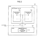
- FIG. 2 is a functional block diagram illustrating the configuration of the chip 100 according to the present embodiment.
- the chip 100 includes a secondary cache 110 and a core 120.
- the secondary cache 110 is a storage unit that acquires various types of data to be used in the core 120 from an external device (not illustrated) and temporarily stores therein the acquired various types of data.
- the secondary cache 110 according to the present invention includes the RAM macro groups 100a and 100b.
- the RAM macro groups 100a and 100b are units that generate the phase clocks ph1 and ph2 based on an external clock supplied from an outside and phase control signals output from a phase control signal generating circuit 130 (the phase control signal generating circuit 130 will be described below) and perform predetermined processes at timings at which the phase clocks are generated.
- FIG. 3 is a diagram explaining a method by which the phase clocks ph1 and ph2 are generated by the RAM macro group.
- the RAM macro group 100a when the RAM macro group 100a generates ph1, the RAM macro group 100a compares an ON/OFF (high/low) state of the external clock and an ON/OFF (high/low) state of the phase control signal. Then, the RAM macro group 100a sets ph1 to ON (high) and ph2 to OFF (low) when the phase control signal is OFF (low) and the external clock is ON (high). The RAM macro group 100a also sets ph1 to OFF (low) and ph2 to ON (high) when the phase control signal is ON (high).
- the RAM macro group 100a when the RAM macro group 100a generates ph2, the RAM macro group 100a compares an ON/OFF (high/low) state of the external clock and an ON/OFF (high/low) state of the phase control signal. Then, the RAM macro group 100a sets ph1 to OFF (low) and ph2 to ON (high) when the phase control signal is ON (high) and the external clock is ON (high). The RAM macro group 100a also sets ph1 to ON (high) and ph2 to OFF (low) when the phase control signal is OFF (low).
- the RAM macro group 100a generates ph1 and ph2 based on the external clock and the phase control signal as described in FIG. 3 and assigns a predetermined process to each of the generated phase clock signals to perform a pipeline processing.
- FIG. 4 is a diagram explaining pipeline processing performed by the RAM macro group 100a. Because pipeline processing performed by the RAM macro group 100b is similar to pipeline processing performed by the RAM macro group 100a, its description is omitted.
- the RAM macro group 100a executes ad1 (the selection of address) at ph1 (Step S1), executes wl1 (the selection of line to be read) at ph2 (Step S2), and executes read1 (the reading of data), wd1 (the selection of line to be written, and ad2 (the selection of address) at ph1 (Step S3).
- a power consumption becomes large at ph1 at which the reading of data is performed (the power consumption becomes is not less than a predetermined value).
- a power consumption becomes small at ph2 at which the other processes are performed (the power consumption is less than the predetermined value).
- the RAM macro group 100a executes write1 (the writing of data) and wl2 (the selection of line to be read) at ph2 (Step S4), executes read2 (the reading of data) and ad3 (the selection of address) at ph1 (Step S5), executes wl3 (the selection of line to be read) at ph2, and executes read3 (the reading of data) at ph1 (Step S7).
- the core 120 is a control unit that operates based on the external clock input from the outside and includes a computing unit for executing a predetermined program and a primary cache for storing therein various types of data.
- the core 120 performs various processes by using these components.
- the core 120 according to the present invention mounts thereon the phase control signal generating circuit 130.
- the phase control signal generating circuit 130 is a device that generates phase control signals and inputs the generated phase control signals into the RAM macro groups 100a and 100b.
- the phase control signal to be input into the RAM macro group 100a is denoted by pc1
- the phase control signal to be input into the RAM macro group 100b is denoted by pc2.
- the phase control signal generating circuit 130 generates pc1 and pc2 so that an ON/OFF (high/low) timing of pc1 and an ON/OFF (high/low) timing of pc2 are opposite to each other.
- the phase control signal generating circuit 130 generates pc1 and pc2 so that the ON (high) timing of pc1 is the OFF (low) timing of pc2 and the OFF (low) timing of pc1 is the ON (high) timing of pc2.
- FIG. 5 is a diagram illustrating an example of the circuit configuration of the phase control signal generating circuit 130.
- the phase control signal generating circuit 130 includes switches 20 and 21, NOT circuits 22 to 25, AND circuits 26 to 29, and OR circuits 30 and 31.
- the switch 20 of them is a switch that is turned on or off in accordance with an electrical signal S input from the outside. Specifically, the switch 20 is turned off for a time period for which the electrical signal S is ON (high) and the switch 20 is turned on for a time period for which the electrical signal S is OFF (low). When the switch 20 is turned on, "High” is inputted into the NOT circuit 22. It is assumed that the electrical signal S is input from the core 120.
- the switch 21 is a switch that is turned on or off in accordance with an electrical signal R input from the outside. Specifically, the switch 21 is turned on for a time period for which the electrical signal R is ON (high) and the switch 21 is turned off for a time period for which the electrical signal R is OFF (low). When the switch 21 is turned on, "Low” is input into the AND circuit 29. It is assumed that the electrical signal R is input from the core 120.
- the NOT circuit 22 is a circuit that reverses an input signal and inputs the inversed signal into an A terminal of the AND circuit 26. Specifically, when the NOT circuit 22 receives "High”, the NOT circuit 22 inputs "Low” into the A terminal of the AND circuit 26. On the other hand, when the NOT circuit 22 receives "Low”, the NOT circuit 22 inputs "High” into the A terminal of the AND circuit 26.
- the NOT circuit 23 is a circuit that reverses an input signal and inputs the inversed signal into an A terminal of the AND circuit 27. Specifically, when the NOT circuit 23 receives "High”, the NOT circuit 23 inputs "Low” into the A terminal of the AND circuit 27. On the other hand, when the NOT circuit 23 receives "Low”, the NOT circuit 23 inputs "High” into the A terminal of the AND circuit 27.
- the NOT circuit 24 is a circuit that reverses an input signal and inputs the reversed signal into an A terminal of the AND circuit 28. Specifically, when the NOT circuit 24 receives "High”, the NOT circuit 24 inputs "Low” into the A terminal of the AND circuit 28. On the other hand, when the NOT circuit 24 receives "Low”, the NOT circuit 24 inputs "High” into the A terminal of the AND circuit 28.
- the NOT circuit 25 is a circuit that reverses an input signal and inputs the reversed signal into an A terminal of the AND circuit 29. Specifically, when the NOT circuit 25 receives "High”, the NOT circuit 25 inputs "Low” into the A terminal of the AND circuit 29. On the other hand, when the NOT circuit 25 receives "Low”, the NOT circuit 25 inputs "High” into the A terminal of the AND circuit 29.
- the AND circuit 26 is a circuit that performs a logical product on signals input from terminals A and B and inputs the result into an A terminal of the OR circuit 30. Specifically, the AND circuit 26 outputs "High” when the signals input from the terminals A and B are “High” and outputs "Low” when at least one of the signals are "Low”.
- the AND circuit 27 is a circuit that performs a logical product on signals input from terminals A and B and inputs the result into a B terminal of the OR circuit 30. Specifically, the AND circuit 27 outputs "High” when the signals input from the terminals A and B are “High” and outputs "Low” when at least one of the signals are "Low”.
- the AND circuit 28 is a circuit that performs a logical product on signals input from terminals A and B and inputs the result into an A terminal of the OR circuit 31. Specifically, the AND circuit 28 outputs "High” when the signals input from the terminals A and B are “High” and outputs "Low” when at least one of the signals are "Low”.
- the AND circuit 29 is a circuit that performs a logical product on signals input from terminals A and B and inputs the result into a B terminal of the OR circuit 31. Specifically, the AND circuit 29 outputs "High” when the signals input from the terminals A and B are “High” and outputs "Low” when at least one of the signals are "Low”.
- the OR circuit 30 is a circuit that performs a logical sum on signals input from the terminals A and B and inputs the result into the RAM macro group 100a as the phase control signal (pc1). Specifically, the OR circuit 30 outputs "High” when any one of the signals input from the terminals A and B is “High” and outputs "Low” when the signals are “Low”. Moreover, the signal output from the OR circuit 30 is fed back to the NOT circuit 22 and the B terminal of the AND circuit 27.
- the OR circuit 31 is a circuit that performs a logical sum on signals input from the terminals A and B and inputs the result into the RAM macro group 100b as the phase control signal (pc2). Specifically, the OR circuit 31 outputs "High” when any one of the signals input from the terminals A and B is “High” and outputs "Low” when the signals are "Low”. Moreover, the signal output from the OR circuit 31 is fed back to the NOT circuit 24 and the B terminal of the AND circuit 29.
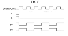
- FIG. 6 is a diagram illustrating a timing chart of the phase control signal generating circuit 130.
- the phase control signals pc1 and pc2 whose on/off states are opposite to each other can be generated by switching the value of the electrical signal S from an initial state “Low” to "High”, switching the value of the electrical signal R from an initial state "High” to “Low”, and inputting the external clock into the phase control signal generating circuit 130.
- FIG. 7 is a timing chart of each phase clock when the phase control signals pc1 and pc2 are input into the RAM macro groups 100a and 100b.
- the timing of ph1 of the RAM macro group 100a coincides with the timing of ph2 of the RAM macro group 100b and the timing of ph2 of the RAM macro group 100a coincides with the timing of ph1 of the RAM macro group 100b.
- the chip (the semiconductor integrated circuit) 100 adjusts a timing at which the phase control signal is turned on or off for each of the RAM macro groups 100a and 100b and distributes the adjusted phase control signal to each of the RAM macro groups 100a and 100b so that the RAM macro groups 100a and 100b do not perform the same process at the same timing. Therefore, the value of current can be constant for each phase clock and thus the increase of the generation of noise and the drop of current can be prevented.
- the chip 100 according to the present embodiment can use the RAM macro groups 100a and 100b without changing the setting of the RAM macro groups 100a and 100b, a manufacturing cost can be reduced.
- each component of each unit illustrated in the drawings is conceptual in functional, and is not necessarily physically configured as illustrated in the drawings. That is, the specific configurations of distribution and integration of the components are not meant to be restricted to those illustrated in the drawings. Therefore, all or a part of the components may be functionally or physically distributed or integrated in arbitrary units in accordance with various types of loads and the state of use.
- the semiconductor integrated circuit and the control signal distribution method according to the present invention are useful for a semiconductor integrated circuit that mounts thereon a RAM macro or the like and particularly is suitable to prevent the increase of noises and the drop of current that occur in the semiconductor integrated circuit.
Landscapes
- Engineering & Computer Science (AREA)
- Theoretical Computer Science (AREA)
- Physics & Mathematics (AREA)
- General Engineering & Computer Science (AREA)
- General Physics & Mathematics (AREA)
- Microelectronics & Electronic Packaging (AREA)
- Semiconductor Integrated Circuits (AREA)
- Static Random-Access Memory (AREA)
- Design And Manufacture Of Integrated Circuits (AREA)
Abstract
Description
- The present invention relates to a semiconductor integrated circuit that generates phase clocks in accordance with an external clock and a control signal and includes a plurality of areas, each of which performs a predetermined process assigned to each phase clock, and a control signal distribution method.
- A RAM macro that performs a predetermined process in synchronization with a clock may generate phase clocks that are used inside the RAM macro in accordance with an external clock in some cases, for example, in order to perform pipeline processing inside the RAM macro (see Patent Document 1). The RAM macro is a circuit configured to perform a predetermined process and is mounted on a chip such as CPU.
- For example, the external clock is classified into two phase clocks, the phase clocks are respectively referred to as a
phase 1 clock (hereinafter, "ph1") and a phase 2 clock (hereinafter, "ph2"), and predetermined processes are assigned to the respective phase clocks. For example, the writing of data and the reading of data are performed at ph1 and the control of word line and the control of memory cell are performed at ph2. When RAM macros as described above are mounted on a chip, such as a CPU, switching between ph1 and ph2 is performed on all the RAM macros in the same manner in many cases because of the convenience of clock distribution and CPU setting. - [Patent Document 1] Japanese Laid-open Patent Publication No.
2002-158286 - However, because switching between ph1 and ph2 is performed on RAM macros mounted on a chip, such as a CPU, in the same manner in the conventional art, there is a problem that the generation of noise and the power supply drop increase.
-
FIG. 8 is a diagram explaining the problem of a conventional art. As illustrated inFIG. 8 , achip 10 mounts thereonRAM macro groups RAM macro groups - The waveform located at the first stage on the right side of the drawing represents a current waveform for phase clocks of the
RAM macro group 10a, the waveform located at the second stage on the right side represents a current waveform for phase clocks of theRAM macro group 10b, and the waveform located at the third stage on the right side represents a current waveform for all the phase clocks of theRAM macro groups RAM macro groups - In this manner, when switching between ph1 and ph2 is performed in the same manner, the timings at which currents are large and the timings at which currents are small of the
RAM macro group 10a overlap with those of theRAM macro group 10b (currents are large at the timing of ph1 and currents are small at the timing of ph2 in an example illustrated inFIG. 8 ). The current range for each of ph1 and ph2 has a large difference. Therefore, this leads to increase the generation of noise and the drop of power supply. - The present invention has been achieved in view of the above problems, and an object of the invention is to provide a semiconductor integrated circuit and a control signal distribution method that can prevent the increase of the generation of noise and the current drop.
- To solve the problem described above and achieve the object, the present invention is a semiconductor integrated circuit that includes a plurality of areas, each of which generates phase clocks in accordance with an external clock and control signals and performs a predetermined process assigned to each of the phase clocks. The semiconductor integrated circuit includes a control signal distributing unit that adjusts a timing at which the control signal is turned ON or OFF for each of the areas and distributes the adjusted control signals to the plurality of areas so that the plurality of areas do not perform a same process at a same timing.
- The plurality of areas includes a first area group and a second area group, and the control signal distributing unit adjusts the control signals so that a timing at which the control signal output to the first area group is turned on or off and a timing at which the control signal output to the second area group is turned on or off are opposite to each other.
- The first area group and the second area group perform a first process whose power consumption is not less than a predetermined value for a time period for which the control signal is ON and perform a second process whose which power consumption is less than the predetermined value for a time period for which the control signal is OFF.
- A control signal distribution method is for a semiconductor integrated circuit that includes a plurality of areas, each of which generates phase clocks in accordance with an external clock and control signals and performs a predetermined process assigned to the each of the phase clocks. The control signal distribution method includes an external clock acquiring step of acquiring the external clock; and an control signal distributing step of adjusting a timing at which the control signal is turned ON or OFF for each of the areas and distributing the adjusted control signals to the plurality of areas by using the external clock so that the plurality of areas do not perform a same process at a same timing.
- The plurality of areas includes a first area group and a second area group, and in the control signal distributing step, the control signals is adjusted so that a timing at which the control signal output to the first area group is turned on or off and a timing at which the control signal output to the second area group is turned on or off are opposite to each other.
- According to the present invention, because the control signal distributing unit adjusts a timing at which the control signal is turned ON or OFF for each of the areas and distributes the adjusted control signals to the plurality of areas so that the plurality of areas do not perform the same process at the same timing, it is possible to prevent the increase of the generation of noise and the drop of current.
- Moreover, according to the present invention, because the plurality of areas includes a first area group and a second area group, and the control signal distributing unit adjusts the control signals so that a timing at which the control signal output to the first area group is turned on or off and a timing at which the control signal output to the second area group is turned on or off are opposite to each other, processes performed by the area groups can be different from each other without changing the setting of each area group, and the value of current can be substantially constant at each timing. Therefore, it is possible to prevent the increase of the generation of noise and the drop of current.
- Moreover, according to the present invention, because the first area group and the second area group perform a first process whose power consumption is not less than a predetermined value for a time period for which the control signal is ON and perform a second process whose power consumption is less than the predetermined value for a time period for which the control signal is OFF, the value of current can be substantially constant at each timing.
-
- [
FIG. 1] FIG. 1 is a diagram explaining an outline and a feature of a chip according to the present embodiment. - [
FIG. 2] FIG. 2 is a functional block diagram illustrating the configuration of the chip according to the present embodiment. - [
FIG. 3] FIG. 3 is a diagram explaining a method by which phase clocks ph1 and ph2 are generated by a RAM macro group. - [
FIG. 4] FIG. 4 is a diagram explaining pipeline processing of the RAM macro group. - [
FIG. 5] FIG. 5 is a diagram illustrating an example of the circuit configuration of a phase control signal generating circuit. - [
FIG. 6] FIG. 6 is a diagram illustrating a timing chart of the phase control signal generating circuit. - [
FIG. 7] FIG. 7 is a timing chart of each phase clock when phase control signals pc1 and pc2 are input into the RAM macro groups. - [
FIG. 8] FIG. 8 is a diagram explaining the problem of a conventional art. -
- 10,100
- chip
- 20, 21
- switch
- 22, 23, 24, 25
- NOT circuit
- 26, 27, 28, 29
- AND circuit
- 30, 31
- OR circuit
- 10a, 10b, 100a, 100b
- RAM macro group
- 110
- secondary cache
- 120
- core
- 130
- phase control signal generating circuit
- Exemplary embodiments of a semiconductor integrated circuit and a control signal distribution method according to the present invention will be explained below in detail with reference to the accompanying drawings. The present invention is not limited to the embodiments explained below.
- First, an outline and a feature of a chip (a semiconductor integrated circuit) according to the present embodiment will be explained.
FIG. 1 is a diagram explaining an outline and a feature of achip 100 according to the present embodiment. As illustrated inFIG. 1 , thechip 100 mounts thereon RAMmacro groups
TheRAM macro groups phase 1 clock (hereinafter, "ph1") and a phase 2 clock (hereinafter, "ph2") based on an external clock supplied from an outside and phase control signals supplied from thechip 100. - The
RAM macro groups FIG. 1 , theRAM macro groups - In
FIG. 1 , the waveform located at the first stage on the right side represents a current waveform for phase clocks of theRAM macro group 100a and the waveform located at the second stage on the right side represents a current waveform for phase clocks of theRAM macro group 100b. As illustrated inFIG. 1 , in both theRAM macro groups - As described in
FIG. 8 , when switching between ph1 and ph2 is performed in the same manner, the timings at which currents are large and the timings at which currents are small of theRAM macro group 100a overlap with those of theRAM macro group 100b. The current range for each of ph1 and ph2 has a large difference. Therefore, thechip 100 according to the present embodiment adjusts phase control signals to be input into theRAM macro groups RAM macro group 100a does not overlap with each phase clock of theRAM macro group 100b. In an example illustrated inFIG. 1 , thechip 100 adjusts the phase control signals so that the phase clocks ph1 of theRAM macro group 100a sequentially overlap with the phase clocks ph2 of theRAM macro group 100b. - In this manner, because the
chip 100 according to the present embodiment adjusts the phase control signals, two current waveforms corresponding to two phase clocks applied to theRAM macro groups FIG. 1 ). Therefore, it is possible to prevent the increase of the generation of noise and the drop of power supply. - Next, the configuration of the
chip 100 according to the present embodiment will be explained.FIG. 2 is a functional block diagram illustrating the configuration of thechip 100 according to the present embodiment. As illustrated inFIG. 2 , thechip 100 includes asecondary cache 110 and acore 120. - The
secondary cache 110 is a storage unit that acquires various types of data to be used in the core 120 from an external device (not illustrated) and temporarily stores therein the acquired various types of data. Particularly, thesecondary cache 110 according to the present invention includes theRAM macro groups - The
RAM macro groups signal generating circuit 130 will be described below) and perform predetermined processes at timings at which the phase clocks are generated. - Now, a method by which the phase clocks ph1 and ph2 are generated by the
RAM macro group 100a will be explained. Because a method by which the phase clocks are generated by theRAM macro group 100b is the same as the method by theRAM macro group 100a, its description is omitted.FIG. 3 is a diagram explaining a method by which the phase clocks ph1 and ph2 are generated by the RAM macro group. - As illustrated in
FIG. 3 , when theRAM macro group 100a generates ph1, theRAM macro group 100a compares an ON/OFF (high/low) state of the external clock and an ON/OFF (high/low) state of the phase control signal. Then, theRAM macro group 100a sets ph1 to ON (high) and ph2 to OFF (low) when the phase control signal is OFF (low) and the external clock is ON (high). TheRAM macro group 100a also sets ph1 to OFF (low) and ph2 to ON (high) when the phase control signal is ON (high). - Moreover, when the
RAM macro group 100a generates ph2, theRAM macro group 100a compares an ON/OFF (high/low) state of the external clock and an ON/OFF (high/low) state of the phase control signal. Then, theRAM macro group 100a sets ph1 to OFF (low) and ph2 to ON (high) when the phase control signal is ON (high) and the external clock is ON (high). TheRAM macro group 100a also sets ph1 to ON (high) and ph2 to OFF (low) when the phase control signal is OFF (low). - The
RAM macro group 100a generates ph1 and ph2 based on the external clock and the phase control signal as described inFIG. 3 and assigns a predetermined process to each of the generated phase clock signals to perform a pipeline processing.FIG. 4 is a diagram explaining pipeline processing performed by theRAM macro group 100a. Because pipeline processing performed by theRAM macro group 100b is similar to pipeline processing performed by theRAM macro group 100a, its description is omitted. - As illustrated in
FIG. 4 , theRAM macro group 100a executes ad1 (the selection of address) at ph1 (Step S1), executes wl1 (the selection of line to be read) at ph2 (Step S2), and executes read1 (the reading of data), wd1 (the selection of line to be written, and ad2 (the selection of address) at ph1 (Step S3). Particularly, a power consumption becomes large at ph1 at which the reading of data is performed (the power consumption becomes is not less than a predetermined value). A power consumption becomes small at ph2 at which the other processes are performed (the power consumption is less than the predetermined value). - Next, the
RAM macro group 100a executes write1 (the writing of data) and wl2 (the selection of line to be read) at ph2 (Step S4), executes read2 (the reading of data) and ad3 (the selection of address) at ph1 (Step S5), executes wl3 (the selection of line to be read) at ph2, and executes read3 (the reading of data) at ph1 (Step S7). - Referring back to explanation of
FIG. 2 , thecore 120 is a control unit that operates based on the external clock input from the outside and includes a computing unit for executing a predetermined program and a primary cache for storing therein various types of data. Thecore 120 performs various processes by using these components. Particularly, thecore 120 according to the present invention mounts thereon the phase controlsignal generating circuit 130. - The phase control
signal generating circuit 130 is a device that generates phase control signals and inputs the generated phase control signals into theRAM macro groups RAM macro group 100a is denoted by pc1 and the phase control signal to be input into theRAM macro group 100b is denoted by pc2. - Particularly, the phase control
signal generating circuit 130 according to the present embodiment generates pc1 and pc2 so that an ON/OFF (high/low) timing of pc1 and an ON/OFF (high/low) timing of pc2 are opposite to each other. In other words, the phase controlsignal generating circuit 130 generates pc1 and pc2 so that the ON (high) timing of pc1 is the OFF (low) timing of pc2 and the OFF (low) timing of pc1 is the ON (high) timing of pc2. - Now, the circuit configuration of the phase control
signal generating circuit 130 will be explained.FIG. 5 is a diagram illustrating an example of the circuit configuration of the phase controlsignal generating circuit 130. As illustrated inFIG. 5 , the phase controlsignal generating circuit 130 includesswitches circuits 22 to 25, ANDcircuits 26 to 29, and ORcircuits - The
switch 20 of them is a switch that is turned on or off in accordance with an electrical signal S input from the outside. Specifically, theswitch 20 is turned off for a time period for which the electrical signal S is ON (high) and theswitch 20 is turned on for a time period for which the electrical signal S is OFF (low). When theswitch 20 is turned on, "High" is inputted into theNOT circuit 22. It is assumed that the electrical signal S is input from thecore 120. - The
switch 21 is a switch that is turned on or off in accordance with an electrical signal R input from the outside. Specifically, theswitch 21 is turned on for a time period for which the electrical signal R is ON (high) and theswitch 21 is turned off for a time period for which the electrical signal R is OFF (low). When theswitch 21 is turned on, "Low" is input into the ANDcircuit 29. It is assumed that the electrical signal R is input from thecore 120. - The
NOT circuit 22 is a circuit that reverses an input signal and inputs the inversed signal into an A terminal of the ANDcircuit 26. Specifically, when theNOT circuit 22 receives "High", theNOT circuit 22 inputs "Low" into the A terminal of the ANDcircuit 26. On the other hand, when theNOT circuit 22 receives "Low", theNOT circuit 22 inputs "High" into the A terminal of the ANDcircuit 26. - The
NOT circuit 23 is a circuit that reverses an input signal and inputs the inversed signal into an A terminal of the ANDcircuit 27. Specifically, when theNOT circuit 23 receives "High", theNOT circuit 23 inputs "Low" into the A terminal of the ANDcircuit 27. On the other hand, when theNOT circuit 23 receives "Low", theNOT circuit 23 inputs "High" into the A terminal of the ANDcircuit 27. - The
NOT circuit 24 is a circuit that reverses an input signal and inputs the reversed signal into an A terminal of the ANDcircuit 28. Specifically, when theNOT circuit 24 receives "High", theNOT circuit 24 inputs "Low" into the A terminal of the ANDcircuit 28. On the other hand, when theNOT circuit 24 receives "Low", theNOT circuit 24 inputs "High" into the A terminal of the ANDcircuit 28. - The
NOT circuit 25 is a circuit that reverses an input signal and inputs the reversed signal into an A terminal of the ANDcircuit 29. Specifically, when theNOT circuit 25 receives "High", theNOT circuit 25 inputs "Low" into the A terminal of the ANDcircuit 29. On the other hand, when theNOT circuit 25 receives "Low", theNOT circuit 25 inputs "High" into the A terminal of the ANDcircuit 29. - The AND
circuit 26 is a circuit that performs a logical product on signals input from terminals A and B and inputs the result into an A terminal of theOR circuit 30. Specifically, the ANDcircuit 26 outputs "High" when the signals input from the terminals A and B are "High" and outputs "Low" when at least one of the signals are "Low". - The AND
circuit 27 is a circuit that performs a logical product on signals input from terminals A and B and inputs the result into a B terminal of theOR circuit 30. Specifically, the ANDcircuit 27 outputs "High" when the signals input from the terminals A and B are "High" and outputs "Low" when at least one of the signals are "Low". - The AND
circuit 28 is a circuit that performs a logical product on signals input from terminals A and B and inputs the result into an A terminal of theOR circuit 31. Specifically, the ANDcircuit 28 outputs "High" when the signals input from the terminals A and B are "High" and outputs "Low" when at least one of the signals are "Low". - The AND
circuit 29 is a circuit that performs a logical product on signals input from terminals A and B and inputs the result into a B terminal of theOR circuit 31. Specifically, the ANDcircuit 29 outputs "High" when the signals input from the terminals A and B are "High" and outputs "Low" when at least one of the signals are "Low". - The OR
circuit 30 is a circuit that performs a logical sum on signals input from the terminals A and B and inputs the result into theRAM macro group 100a as the phase control signal (pc1). Specifically, theOR circuit 30 outputs "High" when any one of the signals input from the terminals A and B is "High" and outputs "Low" when the signals are "Low". Moreover, the signal output from theOR circuit 30 is fed back to theNOT circuit 22 and the B terminal of the ANDcircuit 27. - The OR
circuit 31 is a circuit that performs a logical sum on signals input from the terminals A and B and inputs the result into theRAM macro group 100b as the phase control signal (pc2). Specifically, theOR circuit 31 outputs "High" when any one of the signals input from the terminals A and B is "High" and outputs "Low" when the signals are "Low". Moreover, the signal output from theOR circuit 31 is fed back to theNOT circuit 24 and the B terminal of the ANDcircuit 29. - Next, it will be explained about a relationship between the electrical signals S and R, the external clocks, and the phase control signals pc1 and pc2 of the phase control
signal generating circuit 130 described inFIG. 5 .FIG. 6 is a diagram illustrating a timing chart of the phase controlsignal generating circuit 130. As illustrated inFIG. 6 , the phase control signals pc1 and pc2 whose on/off states are opposite to each other can be generated by switching the value of the electrical signal S from an initial state "Low" to "High", switching the value of the electrical signal R from an initial state "High" to "Low", and inputting the external clock into the phase controlsignal generating circuit 130. - Now, it will be explained about a relationship between the phase clocks when the phase control signals pc1 and pc2 are input into the
RAM macro groups FIG. 7 is a timing chart of each phase clock when the phase control signals pc1 and pc2 are input into theRAM macro groups FIG. 7 , because pc1 and pc2 have opposite signals, the timing of ph1 of theRAM macro group 100a coincides with the timing of ph2 of theRAM macro group 100b and the timing of ph2 of theRAM macro group 100a coincides with the timing of ph1 of theRAM macro group 100b. - In this manner, because the timing of ph1 of the
RAM macro group 100a coincides with the timing of ph2 of theRAM macro group 100b and the timing of ph2 of theRAM macro group 100a coincides with the timing of ph1 of theRAM macro group 100b, the magnitude of current is constant for each phase clock. Therefore, it is possible to prevent the increase of the generation of noise and the drop of current. - As described above, the chip (the semiconductor integrated circuit) 100 according to the present embodiment adjusts a timing at which the phase control signal is turned on or off for each of the
RAM macro groups RAM macro groups RAM macro groups - Moreover, because the
chip 100 according to the present embodiment can use theRAM macro groups RAM macro groups - In the meantime, among the processes described in the present embodiment, all or a part of processes explained as being automatically performed may be manually performed. Alternatively, all or a part of processes explained as being manually performed may be automatically performed through a known method. In addition, the process procedures, control procedures, specific names, and information including various types of data and parameters described in the specification and illustrated in the drawings can be arbitrarily changed unless otherwise specified.
- Each component of each unit illustrated in the drawings is conceptual in functional, and is not necessarily physically configured as illustrated in the drawings. That is, the specific configurations of distribution and integration of the components are not meant to be restricted to those illustrated in the drawings. Therefore, all or a part of the components may be functionally or physically distributed or integrated in arbitrary units in accordance with various types of loads and the state of use.
- As described above, the semiconductor integrated circuit and the control signal distribution method according to the present invention are useful for a semiconductor integrated circuit that mounts thereon a RAM macro or the like and particularly is suitable to prevent the increase of noises and the drop of current that occur in the semiconductor integrated circuit.
Claims (6)
- A semiconductor integrated circuit that includes a plurality of areas, each of which generates phase clocks in accordance with an external clock and control signals and performs a predetermined process assigned to each of the phase clocks, the semiconductor integrated circuit comprising:a control signal distributing unit that adjusts a timing at which the control signal is turned ON or OFF for each of the areas and distributes the adjusted control signals to the plurality of areas so that the plurality of areas do not perform a same process at a same timing.
- The semiconductor integrated circuit according to claim 1, wherein
the plurality of areas includes a first area group and a second area group, and
the control signal distributing unit adjusts the control signals so that a timing at which the control signal output to the first area group is turned on or off and a timing at which the control signal output to the second area group is turned on or off are opposite to each other. - The semiconductor integrated circuit according to claim 1 or 2, wherein the first area group and the second area group perform a first process whose power consumption is not less than a predetermined value for a time period for which the control signal is ON and perform a second process whose which power consumption is less than the predetermined value for a time period for which the control signal is OFF.
- A control signal distribution method for a semiconductor integrated circuit that includes a plurality of areas, each of which generates phase clocks in accordance with an external clock and control signals and performs a predetermined process assigned to the each of the phase clocks, the control signal distribution method comprising:an external clock acquiring step of acquiring the external clock; andan control signal distributing step of adjusting a timing at which the control signal is turned ON or OFF for each of the areas and distributing the adjusted control signals to the plurality of areas by using the external clock so that the plurality of areas do not perform a same process at a same timing.
- The control signal distribution method according to claim 4, wherein
the plurality of areas includes a first area group and a second area group, and
in the control signal distributing step, the control signals is adjusted so that a timing at which the control signal output to the first area group is turned on or off and a timing at which the control signal output to the second area group is turned on or off are opposite to each other. - The control signal distribution method according to claims 4 or 5, wherein the first area group and the second area group perform a first process whose power consumption is not less than a predetermined value for a time period for which the control signal is ON and perform a second process whose which power consumption is less than the predetermined value for a time period for which the control signal is OFF.
Applications Claiming Priority (1)
| Application Number | Priority Date | Filing Date | Title |
|---|---|---|---|
| PCT/JP2007/056967 WO2008126229A1 (en) | 2007-03-29 | 2007-03-29 | Semiconductor integrated circuit and control signal distributing method |
Publications (2)
| Publication Number | Publication Date |
|---|---|
| EP2136396A1 true EP2136396A1 (en) | 2009-12-23 |
| EP2136396A4 EP2136396A4 (en) | 2010-06-02 |
Family
ID=39863410
Family Applications (1)
| Application Number | Title | Priority Date | Filing Date |
|---|---|---|---|
| EP07740405A Withdrawn EP2136396A4 (en) | 2007-03-29 | 2007-03-29 | INTEGRATED SEMICONDUCTOR CIRCUIT AND METHOD FOR CONTROLLING SIGNAL DISTRIBUTION |
Country Status (4)
| Country | Link |
|---|---|
| US (1) | US7999594B2 (en) |
| EP (1) | EP2136396A4 (en) |
| JP (1) | JP4774119B2 (en) |
| WO (1) | WO2008126229A1 (en) |
Family Cites Families (10)
| Publication number | Priority date | Publication date | Assignee | Title |
|---|---|---|---|---|
| US5666322A (en) * | 1995-09-21 | 1997-09-09 | Nec Electronics, Inc. | Phase-locked loop timing controller in an integrated circuit memory |
| JP3345282B2 (en) * | 1996-06-10 | 2002-11-18 | 株式会社日立製作所 | Design method of semiconductor integrated circuit device |
| TW318933B (en) | 1996-03-08 | 1997-11-01 | Hitachi Ltd | Semiconductor IC device having a memory and a logic circuit implemented with a single chip |
| JP4552258B2 (en) | 2000-03-29 | 2010-09-29 | エルピーダメモリ株式会社 | Semiconductor memory device |
| JP3620440B2 (en) | 2000-11-20 | 2005-02-16 | 日本電気株式会社 | Semiconductor integrated circuit and clock distribution method thereof |
| US20060194160A1 (en) | 2003-03-10 | 2006-08-31 | Shinji Kokuo | Gas combustion-control method and gas combustion device |
| US8190808B2 (en) | 2004-08-17 | 2012-05-29 | Rambus Inc. | Memory device having staggered memory operations |
| JP4343859B2 (en) * | 2005-02-17 | 2009-10-14 | 株式会社日立製作所 | Semiconductor device |
| KR100665232B1 (en) * | 2005-12-26 | 2007-01-09 | 삼성전자주식회사 | Synchronous Semiconductor Memory Device |
| US7616043B2 (en) * | 2008-02-12 | 2009-11-10 | Sony Computer Entertainment Inc. | Methods and apparatus for managing LSI power consumption and degradation using clock signal conditioning |
-
2007
- 2007-03-29 JP JP2009508779A patent/JP4774119B2/en not_active Expired - Fee Related
- 2007-03-29 WO PCT/JP2007/056967 patent/WO2008126229A1/en not_active Ceased
- 2007-03-29 EP EP07740405A patent/EP2136396A4/en not_active Withdrawn
-
2009
- 2009-09-29 US US12/585,962 patent/US7999594B2/en not_active Expired - Fee Related
Also Published As
| Publication number | Publication date |
|---|---|
| JPWO2008126229A1 (en) | 2010-07-22 |
| US7999594B2 (en) | 2011-08-16 |
| EP2136396A4 (en) | 2010-06-02 |
| US20100019823A1 (en) | 2010-01-28 |
| WO2008126229A1 (en) | 2008-10-23 |
| JP4774119B2 (en) | 2011-09-14 |
Similar Documents
| Publication | Publication Date | Title |
|---|---|---|
| US6614700B2 (en) | Circuit configuration with a memory array | |
| KR960010963B1 (en) | Memory device with test function | |
| US20120155200A1 (en) | Memory device, memory system including the same, and control method thereof | |
| KR20110093086A (en) | Semiconductor memory device using internal high power supply voltage in self-refresh mode and method for applying high power supply voltage | |
| US7558979B2 (en) | Methods for determining simultaneous switching induced data output timing skew | |
| EP1606823B1 (en) | Two-dimensional data memory | |
| EP2136396A1 (en) | Semiconductor integrated circuit and control signal distributing method | |
| US6385746B1 (en) | Memory test circuit | |
| US7457185B2 (en) | Semiconductor memory device with advanced refresh control | |
| JPH1092175A (en) | Cas signal generator of synchronous dram | |
| US6704243B2 (en) | Apparatus for generating memory-internal command signals from a memory operation command | |
| US20040260934A1 (en) | Memory chip having an integrated address scrambler unit and method for scrambling an address in an integrated memory | |
| US6772271B2 (en) | Reduction of bank switching instructions in main memory of data processing apparatus having main memory and plural memory | |
| JP2004022014A (en) | Semiconductor device and method for testing the same | |
| US20010012290A1 (en) | Data input circuit and semiconductor device utilizing data input circuit | |
| CN110322911B (en) | Method and system for controlling retention margin of semiconductor memory device | |
| US6707705B2 (en) | Integrated dynamic memory device and method for operating an integrated dynamic memory | |
| JP2005267369A (en) | Memory control device and method | |
| KR20190020411A (en) | Arbitrary circuit for pseudo dual port memory | |
| JP2573068B2 (en) | Digital pattern generator | |
| CN119181406A (en) | Nonvolatile memory, operation method of nonvolatile memory and electronic device | |
| US8836360B2 (en) | Semiconductor device including integrated circuit | |
| KR20030023337A (en) | Test mode entry method of semiconductor memory device and disposition of test mode line using it | |
| KR100481828B1 (en) | Control method of memory using a variable address control circuit | |
| KR0116915Y1 (en) | Dynamic memory |
Legal Events
| Date | Code | Title | Description |
|---|---|---|---|
| PUAI | Public reference made under article 153(3) epc to a published international application that has entered the european phase |
Free format text: ORIGINAL CODE: 0009012 |
|
| 17P | Request for examination filed |
Effective date: 20091026 |
|
| AK | Designated contracting states |
Kind code of ref document: A1 Designated state(s): AT BE BG CH CY CZ DE DK EE ES FI FR GB GR HU IE IS IT LI LT LU LV MC MT NL PL PT RO SE SI SK TR |
|
| A4 | Supplementary search report drawn up and despatched |
Effective date: 20100507 |
|
| RIC1 | Information provided on ipc code assigned before grant |
Ipc: H01L 27/04 20060101ALI20100429BHEP Ipc: H01L 21/822 20060101AFI20081104BHEP Ipc: G11C 7/10 20060101ALI20100429BHEP |
|
| DAX | Request for extension of the european patent (deleted) | ||
| 17Q | First examination report despatched |
Effective date: 20110519 |
|
| RIC1 | Information provided on ipc code assigned before grant |
Ipc: G11C 8/18 20060101ALI20131011BHEP Ipc: G11C 7/22 20060101AFI20131011BHEP Ipc: G06F 1/32 20060101ALI20131011BHEP Ipc: G11C 7/10 20060101ALI20131011BHEP |
|
| GRAC | Information related to communication of intention to grant a patent modified |
Free format text: ORIGINAL CODE: EPIDOSCIGR1 |
|
| GRAP | Despatch of communication of intention to grant a patent |
Free format text: ORIGINAL CODE: EPIDOSNIGR1 |
|
| INTG | Intention to grant announced |
Effective date: 20131213 |
|
| INTG | Intention to grant announced |
Effective date: 20131216 |
|
| STAA | Information on the status of an ep patent application or granted ep patent |
Free format text: STATUS: THE APPLICATION IS DEEMED TO BE WITHDRAWN |
|
| 18D | Application deemed to be withdrawn |
Effective date: 20140429 |