EP2136378A1 - Electronic component - Google Patents
Electronic component Download PDFInfo
- Publication number
- EP2136378A1 EP2136378A1 EP09251572A EP09251572A EP2136378A1 EP 2136378 A1 EP2136378 A1 EP 2136378A1 EP 09251572 A EP09251572 A EP 09251572A EP 09251572 A EP09251572 A EP 09251572A EP 2136378 A1 EP2136378 A1 EP 2136378A1
- Authority
- EP
- European Patent Office
- Prior art keywords
- electrode
- internal electrode
- width
- electronic component
- axis direction
- Prior art date
- Legal status (The legal status is an assumption and is not a legal conclusion. Google has not performed a legal analysis and makes no representation as to the accuracy of the status listed.)
- Granted
Links
Images


Classifications
-
- H—ELECTRICITY
- H01—ELECTRIC ELEMENTS
- H01C—RESISTORS
- H01C7/00—Non-adjustable resistors formed as one or more layers or coatings; Non-adjustable resistors made from powdered conducting material or powdered semi-conducting material with or without insulating material
- H01C7/04—Non-adjustable resistors formed as one or more layers or coatings; Non-adjustable resistors made from powdered conducting material or powdered semi-conducting material with or without insulating material having negative temperature coefficient
-
- H—ELECTRICITY
- H01—ELECTRIC ELEMENTS
- H01C—RESISTORS
- H01C7/00—Non-adjustable resistors formed as one or more layers or coatings; Non-adjustable resistors made from powdered conducting material or powdered semi-conducting material with or without insulating material
- H01C7/18—Non-adjustable resistors formed as one or more layers or coatings; Non-adjustable resistors made from powdered conducting material or powdered semi-conducting material with or without insulating material comprising a plurality of layers stacked between terminals
-
- H—ELECTRICITY
- H01—ELECTRIC ELEMENTS
- H01C—RESISTORS
- H01C7/00—Non-adjustable resistors formed as one or more layers or coatings; Non-adjustable resistors made from powdered conducting material or powdered semi-conducting material with or without insulating material
- H01C7/04—Non-adjustable resistors formed as one or more layers or coatings; Non-adjustable resistors made from powdered conducting material or powdered semi-conducting material with or without insulating material having negative temperature coefficient
- H01C7/041—Non-adjustable resistors formed as one or more layers or coatings; Non-adjustable resistors made from powdered conducting material or powdered semi-conducting material with or without insulating material having negative temperature coefficient formed with two or more layers
-
- H—ELECTRICITY
- H01—ELECTRIC ELEMENTS
- H01C—RESISTORS
- H01C7/00—Non-adjustable resistors formed as one or more layers or coatings; Non-adjustable resistors made from powdered conducting material or powdered semi-conducting material with or without insulating material
- H01C7/008—Thermistors
Definitions
- the present invention relates to electronic components, and an electronic component that incorporates a thermistor.
- FIG. 10A illustrates the laminated thermistor 110 viewed from the lamination direction (z-axis direction), and Fig. 10B is a cross-sectional view of the laminated thermistor 110 in an xy plane.
- the laminated thermistor 110 includes an internal electrode 106a connected to an external electrode 114a, an internal electrode 106b connected to an external electrode 114b, and an internal electrode 107 overlapping the internal electrodes 106a and 106b.
- An electronic component that incorporates a thermistor is used in various devices, such as a cellular phone, a personal computer, or a power supply component. To support various uses, it is desired for such an electronic component incorporating a thermistor to allow variations in the value of resistance of the thermistor to be increased without a significant change of thermistor characteristics, such as a decried rate of change of resistance or breakdown voltage.
- the value of resistance in the laminated thermistor 110 depends on the sum of the area S11 of the region E11 where the internal electrode 106a and the internal electrode 107 overlap each other and the area S12 of the region E12 where the internal electrode 106b and the internal electrode 107 overlap each other.
- One possible approach to adjusting the value of resistance in the laminated thermistor 110 is to change the sum of the areas S11 and S12 of the two regions E11 and E12.
- the laminated thermistor 110 because, even if the internal electrode 107 is displaced in its x-axis direction and the area S11 of the region E11, where the internal electrode 106a and the internal electrode 107 overlap each other, is increased, the area S12 of the region E12, where the internal electrode 106b and the internal electrode 107 overlap each other, is reduced, the sum of the two areas S11 and S12 is constant. Accordingly, in order to change the value of resistance in the laminated thermistor 110, it is necessary to change the design, for example, the size or shape, of the internal electrodes 106a, 106b, and 107 for each of various thermistors.
- Embodiments of the present invention provide an electronic component allowing its value of resistance to be changed without a significant change of its basic structure, and in particular, allowing fine adjustment to the value of resistance.
- the invention is defined in the independent claims to which reference is now directed. Preferred features are set out in the dependent claims.
- an electronic component includes a layered structure, a first external electrode and a second external electrode, an isolated electrode, a first internal electrode, and a second internal electrode.
- the layered structure includes laminated ceramic layers.
- the first external electrode and a second external electrode are disposed on a surface of the layered structure.
- the isolated electrode extends in a predetermined direction inside the layered structure and is unconnected to the first external electrode and the second external electrode.
- the first internal electrode is connected to the first external electrode.
- the first internal electrode faces a first end of the isolated electrode such that one of the ceramic layers is disposed therebetween.
- the second internal electrode is connected to the second external electrode.
- the second internal electrode faces a second end of the isolated electrode such that one of the ceramic layers is disposed therebetween.
- the isolated electrode When viewed in plan from a direction in which the ceramic layers are laminated, the isolated electrode includes a non-overlapping portion including a first section having a first width between opposite ends thereof and a second section having a second width between opposite ends thereof, and the first width is larger than the second width, the non-overlapping portion not overlapping the first internal electrode and the second internal electrode, the first section being adjacent to the first internal electrode or the second internal electrode, the second section being adjacent the other one of the first internal electrode and the second internal electrode, the first width and the second width being substantially perpendicular to the predetermined direction.
- the first width is larger than the second width.
- the amount of increase or decrease in the area of the overlapping portion between the first internal electrode and the isolated electrode is larger than the amount of increase or decrease in the area of the overlapping portion between the second internal electrode and the isolated electrode. Accordingly, the sum of the area of the overlapping portion between the first internal electrode and the isolated electrode and the area of the overlapping portion between the second internal electrode and the isolated electrode can be increased or reduced, and the value of resistance of the electronic component can be reduced or increased. As a result, fine adjustment of the value of resistance can be made merely by movement of the isolated electrode without having to change the design of the isolated electrode, for example, the size or shape.
- the first width may be larger than the second width even when the isolated electrode is moved in the predetermined direction.
- the isolated electrode may have a width being substantially perpendicular to the predetermined direction and reducing in a direction from the first end to the second end thereof, and each of the first internal electrode and the second internal electrode may have a width being substantially perpendicular to the predetermined direction and being equal to or larger than each of the width of the isolated electrode at the first end and the width of the isolated electrode at the second end.
- the width of the isolated electrode being substantially perpendicular to the predetermined direction reduces in the direction from the first end to the second end of the isolated electrode.
- the first width is always larger than the second width.
- the range of the adjustment of the value of resistance can be increased by an increase in the amount of movement of the isolated electrode.
- each of the width of the first internal electrode and the width of the second internal electrode substantially perpendicular to the predetermined direction are equal to or larger than each of the width of the isolated electrode at the first end and that at the second end.
- the isolated electrode is less prone to projecting from the first and second internal electrodes. As a result, unevenness of the value of resistance of the electronic component can be suppressed.
- the isolated electrode may include a space that has no conductive film, and the space may have a width being substantially perpendicular to the predetermined direction and increasing in a direction from the first end to the second end of the isolated electrode. Therefore, the outer shape of the isolated electrode can remain substantially rectangular, and this can suppress unevenness of the value of resistance.
- each of the isolated electrode, the first internal electrode, and the second internal electrode may have a width being substantially perpendicular to the predetermined direction and increasing in a direction from the first end to the second end of the isolated electrode.
- the isolated electrode, the first internal electrode, and the second internal electrode may have substantially the same electrode pattern. Therefore, the isolated electrode, the first internal electrode, and the second internal electrode can be formed using one kind of electrode pattern. Therefore, the efficiency in manufacturing the electronic component is enhanced.
- the first width at opposite ends of the first section of the non-overlapping portion of the isolated electrode which does not overlap the first internal electrode and the second internal electrode and is in contact with the first internal electrode is larger than the second width at opposite ends of the second section of the non-overlapping portion of the isolated electrode in contact with the second internal electrode.
- the electronic component is a laminated electronic component that incorporates a negative temperature coefficient (NTC) thermistor.
- NTC negative temperature coefficient
- Fig. 1 is an external perspective view of an electronic component 10a according to an embodiment of the present invention.
- Fig. 2 is an exploded view of a layered structure 12 of the electronic component 10a.
- the direction in which ceramic green sheets are laminated in the process of forming the electronic component 10a is defined as the lamination direction. That lamination direction indicates a z-axis direction; the substantially longitudinal direction of the electronic component 10a indicates an x-axis direction; and a direction substantially perpendicular to the x-axis and z-axis indicates a y-axis direction.
- the x-axis, y-axis, and z-axis are substantially perpendicular to a corresponding side of the electronic component 10a.
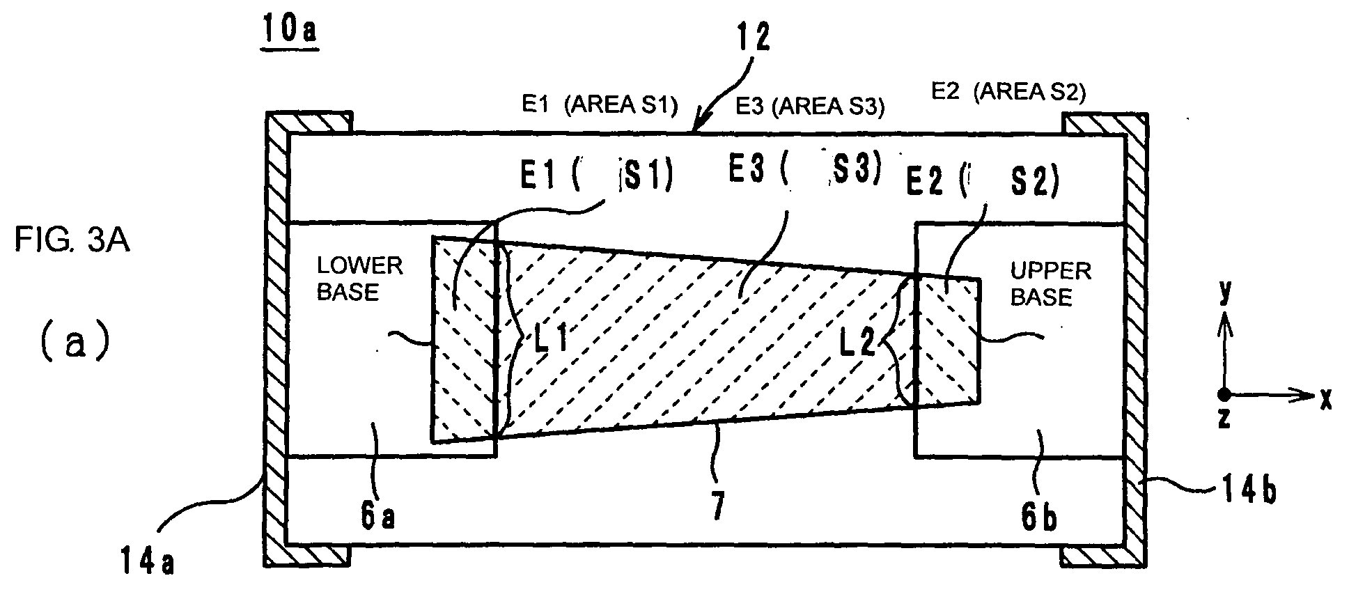
- Fig. 3A illustrates the electronic component 10a viewed in plan from the z-axis direction.
- Fig. 3B is a cross-sectional view of the electronic component 10a in an xy plane.
- the electronic component 10a includes the substantially rectangular parallelepiped layered structure 12 and external electrodes 14a and 14b disposed on the surface of the layered structure 12.
- the layered structure 12 incorporates a thermistor.
- the external electrodes 14a and 14b are disposed so as to cover respective side faces of the layered structure 12 at opposite ends in the x-axis direction.
- the layered structure 12 includes a plurality of internal electrodes and ceramic layers laminated together and incorporates the thermistor, as described below. More specifically, the layered structure 12 is formed by lamination of a plurality of ceramic layers 5a, 5b, 5c, 4a, 4b, 5d, 5e, and 5f in this order, as illustrated in Fig. 2 .
- the plurality of ceramic layers 5a to 5c, 4a, 4b, and 5d to 5f are substantially rectangular semiconductor layers having substantially the same area and shape.
- a substantially rectangular internal electrode 6a is disposed on a principal surface of the ceramic layer 4a.
- the internal electrode 6a substantially vertically extends from a short side of the ceramic layer 4a placed in the negative x-axis direction to the positive x-axis direction.
- the internal electrode 6a is connected to the external electrode 14a at the short side placed in the negative x-axis direction, as illustrated in Figs. 3A and 3B .
- a substantially rectangular internal electrode 6b is disposed on the principal surface of the ceramic layer 4a.
- the internal electrode 6b substantially vertically extends from a short side of the ceramic layer 4a placed in the positive x-axis direction to the negative x-axis direction.
- the internal electrode 6b is connected to the external electrode 14b at the short side placed in the positive x-axis direction, as illustrated in Figs. 3A and 3B .
- the internal electrodes 6a and 6b have substantially the same width in the y-axis direction.
- the internal electrodes 6a and 6b are aligned in a line along the x-axis direction and are separated by a predetermined gap.
- a substantially isosceles trapezoidal internal electrode 7 (isolated or unconnected electrode) is disposed on a principal surface of the ceramic layer 4b.
- the internal electrode 7 extends in the x-axis direction and is not connected to the external electrodes 14a and 14b. More specifically, as illustrated in Fig. 3A , the width of the internal electrode 7 in the y-axis direction reduces in the direction from a side placed on an end in the negative x-axis direction (hereinafter referred to as the lower base) to another side placed on an end in the positive x-axis direction (hereinafter referred to as the upper base).
- the height direction of the substantially isosceles trapezoidal internal electrode 7 is substantially the same as the x-axis direction.
- the internal electrode 6a when viewed in plan from the z-axis direction, faces the lower base of the internal electrode 7 such that the ceramic layer 4a is disposed therebetween.
- the internal electrode 6b faces the upper base of the internal electrode 7 such that the ceramic layer 4a is disposed therebetween.
- the ceramic layer 4a and the internal electrodes 7, 6a, and 6b constitute the thermistor.
- the ceramic layers 5a to 5c, 4a, 4b, and 5d to 5f illustrated in the exploded perspective view of Fig. 2 are laminated in this order from above in the z-axis direction to form the layered structure 12.
- the external electrodes 14a and 14b are formed on the surface of the layered structure 12. In such a way, the electronic component 10a is obtained.
- the electronic component 10a formed in the above-described way allows the value of resistance to be both increased and reduced without a change of the design of the internal electrode 7, for example the size or shape, thus enabling fine adjustment of the value of resistance, as described below with reference to Figs. 3 to 5 .
- the value of resistance can be increased by the movement of the internal electrode 7 in the positive x-axis direction and can be reduced by the movement of the internal electrode 7 in the negative x-axis direction. That is, for the electronic component 10a, the value of resistance of the electronic component 10a illustrated in Figs. 3A and 3B can be increased and reduced, thus enabling the electronic component to have various values of resistance. Fine adjustment of the value of resistance of the electronic component 10a can be made without having to change the design of the internal electrode 7, for example, the size or shape.
- Fig. 4A illustrates the electronic component 10a viewed in plan from the z-axis direction when the internal electrode 7 is moved by ⁇ L in the positive x-axis direction from the state shown in Figs. 3A and 3B .
- Fig. 4B illustrates the amount of decrease in the area of a portion where the internal electrode 6a and the internal electrode 7 overlap each other.
- Fig. 4C illustrates the amount of increase in the area of a portion where the internal electrode 6b and the internal electrode 7 overlap each other.
- Fig. 5A illustrates the electronic component 10a viewed in plan from the z-axis direction when the internal electrode 7 is moved by ⁇ L in the negative x-axis direction from the state illustrated in Figs. 3A and 3B .
- Fig. 5B is a cross-sectional view of the electronic component 10a illustrated in Fig. 5A in an xy plane.
- a region E1 indicates a region of the internal electrode 7 that overlaps the internal electrode 6a
- a region E2 indicates a region of the internal electrode 7 that overlaps the internal electrode 6b
- a region E3 indicates a region of the internal electrode 7 that overlaps neither of the internal electrodes 6a and 6b.
- the region E1 has an area S1
- the region E2 has an area S2
- the region E3 has an area S3.
- the internal electrode 6a has a width in the y-axis direction that is slightly larger than the width of the lower base of the internal electrode 7 in the y-axis direction.
- the internal electrode 6b has a width in the y-axis direction that is larger than the width of the upper base of the internal electrode 7 in the y-axis direction.
- a width L1 in the y-axis direction between the opposite ends of a portion of the region E3 that is in contact with the internal electrode 6a in plan view is larger than a width L2 in the y-axis direction between the opposite ends of a portion of the region E3 that is in contact with the internal electrode 6b in plan view.
- the amount of increase and decrease in the area S1 of the region E1 can be larger than that in the area S2 of the region E2 when the internal electrode 7 is moved in the x-axis direction. That is, the area S3 of the region E3 can be increased and reduced merely by the movement of the internal electrode 7 without a change of the shape of the internal electrode 6a, 6b, or 7. The details are described below.
- the area S1 of the region E1 is reduced by the area ⁇ S1 corresponding to a substantially isosceles trapezoidal region ⁇ E1.
- the amount of movement of the internal electrode 7 to adjust the value of resistance is no more than 0.05 mm. Accordingly, the region ⁇ E1 can be approximated to a rectangle having the length L1 and the width ⁇ L, as illustrated in Fig. 4B .
- the area S2 of the region E2 is increased by the area ⁇ S2 corresponding to a substantially isosceles trapezoidal region ⁇ E2. Accordingly, the region ⁇ E2 can be approximated to a rectangle having the length L2 and the width ⁇ L, as illustrated in Fig. 4C .
- the area ⁇ S1 of the region ⁇ E1 and the area ⁇ S2 of the region ⁇ E2 are compared with each other, because the width L1 is larger than the width L2, the area ⁇ S1 is larger than the area ⁇ S2. That is, in the electronic component 10a, the sum of the areas of the overlapping portions where the internal electrodes 6a and 6b overlap the internal electrode 7, i.e., the sum of the area S1 of the region E1 and the area S2 of the region E2 can be reduced by the movement of the internal electrode 7 in the positive x-axis direction.
- the value of resistance of the electronic component 10a depends on the sum of the areas S1 and S2. When the sum of the areas S1 and S2 is reduced by the movement of the internal electrode 7 in the positive x-axis direction, the value of resistance of the electronic component 10a is increased.
- the internal electrodes 6a, 6b, and 7 in the electronic component 10a have a structure and arrangement in which the width L1 is larger than the width L2. Accordingly, the value of resistance of the electronic component 10a can be reduced or increased by the movement of the internal electrode 7 in the positive x-axis direction or the negative x-axis direction. As a result, fine adjustment of the value of resistance can be made without having to change the design of the internal electrode 7, for example, the size or shape.
- the width of the internal electrode 7 in the y-axis direction reduces in the positive x-axis direction, as illustrated in Fig. 3A .
- the width L1 is always larger than the width L2. Accordingly, in the electronic component 10a, an increase in the amount of movement of the internal electrode 7 enables an increase in the range of adjustment of the value of resistance.
- each of the width of the internal electrode 6a in the y-axis direction and the width of the internal electrode 6b in the y-axis direction is larger than each of the length of the lower base of the internal electrode 7 and the length of the upper base of the internal electrode 7. Accordingly, even if the internal electrode 7 is displaced by misregistration in laminating ceramic green sheets in the process of forming the layered structure 12 of the electronic component 10a, the internal electrode 7 is less prone to projecting from the edges of the internal electrodes 6a, 6b, and 7 in the y-axis direction. As a result, unevenness of the value of resistance of the electronic component 10a can be suppressed.
- an electronic component having a desired value of resistance may be unobtainable.
- the internal electrode 7 may be moved in the x-axis direction.
- Figs. 6A to 6C illustrate models used in the simulation.
- Fig. 6A illustrates a first model corresponding to the electronic component 10a viewed in plan from the z-axis direction.
- Fig. 6B illustrates a second model corresponding to the laminated thermistor described in the patent document previously mentioned in the description of the related art viewed in plan from the z-axis direction.
- Fig. 6C is a cross-sectional view of the first and second models in an xy plane.
- the internal electrodes 6a, 6b, 7, 106a, 106b, and 107 of the two models illustrated in Figs. 6A and 6B were moved in the x-axis direction, and the values of resistance of the electronic component 10a and the laminated thermistor 110 were calculated.
- the conditions of the simulation are described below.
- the model of 0603 chip size (approximately 0.6 mm ⁇ 0.3 mm ⁇ 0.3 mm) is used, and the internal electrodes 6a, 6b, and 7 are disposed, similar to the electronic component 10a illustrated in Figs. 3A and 3B .
- the two internal electrodes 6a and the two internal electrodes 6b are disposed, and the internal electrode 7 is sandwiched between the two internal electrodes 6a and between the two internal electrodes 6b.
- the length L11 of the upper base of the internal electrode 7 is approximately 0.16 mm
- the length L12 of the lower base thereof is approximately 0.2 mm
- the height L13 thereof is approximately 0.405 mm.
- the width L12 of each of the internal electrodes 6a and 6b is approximately 0.2 mm.
- the gap between the internal electrodes 6a and 6b is indicated by L15.
- the model of 0603 chip size (approximately 0.6 mm ⁇ 0.3 mm ⁇ 0.3 mm) is used, and the internal electrodes 106a, 106b, and 107 are disposed, similar to the laminated thermistor 110 illustrated in Figs. 10A and 10B .
- the two internal electrodes 106a and the two internal electrodes 106b are disposed, and the internal electrode 107 is sandwiched between the two internal electrodes 106a and between the two internal electrodes 106b.
- the width L21 of the internal electrode 107 is approximately 0.2 mm, and the height L23 thereof is approximately 0.38 mm.
- the width L21 of each of the internal electrodes 106a and 106b is approximately 0.2 mm.
- the gap between the internal electrodes 106a and 106b is indicated by L25.
- the values of resistance were calculated when the internal electrodes 7 and 107 were displaced by approximately ⁇ 0.05 mm in the x-axis direction from the respective reference positions.
- the reference position for the internal electrode 7 is the position of the internal electrode 7 when the overlap portion between the internal electrodes 7 and 6a and the overlap portion between the internal electrodes 7 and 6b have substantially the same width in the x-axis direction.
- the reference position for the internal electrode 107 indicates the position thereof when the overlap portion between the internal electrodes 107 and 106a and the overlap portion between the internal electrodes 107 and 106b have substantially the same width in the x-axis direction.
- Fig. 7 is a graph that illustrates the results of the simulation. The vertical axis indicates the values of resistance, and the horizontal axis indicates the magnitudes of the gaps.
- the simulation reveals that the value of resistance in the laminated thermistor described in the above-mentioned patent document cannot be changed even by the movement of the internal electrode 107, whereas the value of resistance in the electronic component 10a can be changed by the movement of the internal electrode 7.
- minute changes in the value of resistance can be made. Accordingly, the use of the electronic components 10a results in obtainment of an electronic component having various values of resistance.
- the value of resistance is approximately 11 k ⁇ and remains invariant. Also, even when the gap L25 is incremented by approximately 0.01 mm, the value of resistance can only be changed discontinuously in units of approximately 0.4 k ⁇ to 0.5 k ⁇ . In contrast to this, in the first model, as illustrated in Fig. 7 , when the gap L15 is increased by approximately 0.01 mm, the value of resistance is reduced by approximately 0.4 k ⁇ to 0.5 k ⁇ .
- the value of resistance is changed by approximately 0.4 k ⁇ to 0.5 k ⁇ . That is, in the first model, the value of resistance can be continuously changed in the range of approximately 8.9 k ⁇ to 11.2 k ⁇ by the adjustment of the gap L15 in units of approximately 0.01 mm and the movement of the internal electrode 7 in units of approximately 0.05 mm. In other words, in the electronic component 10a, the value of resistance can be adjusted more minutely in a wider range.
- a small amount of displacement of the value of resistance resulting from print blurring or light printing of the internal electrodes 6a, 6b, and 7 can be corrected by adjustment of the amount of movement of the internal electrode 7 and the magnitude of the gap L15.
- the value of resistance of the electronic component 10a can be reduced or increased by the movement of the internal electrode 7 in the positive or negative x-axis direction because the internal electrode 7 has a substantially isosceles trapezoidal shape.
- the value of resistance of the electronic component can be reduced or increased from substantially the same principle by the use of a structure and arrangement in which the width L1 is larger than the width L2 in the internal electrodes 6a, 6b, and 7.
- Modified examples of the electronic component 10a are described below with reference to the drawings.
- Figs. 8A to 8C and 9A and 9B illustrate electronic components 10b to 10f according to the modified examples viewed in plan from the z-axis direction.
- Fig. 8A illustrates the electronic component 10b according to a first modified example viewed in plan from the z-axis direction.
- the internal electrode 7 included in the electronic component 10b has the shape of a combination of a substantially rectangle and a substantially semicircle. More specifically, the internal electrode 7 has a shape in which the substantially semicircular electrode is coupled to a portion of the substantially rectangular electrode in the positive x-axis direction. Even in the electronic component 10b including the internal electrode 7 having such a shape, the width L1 is larger than the width L2. As a result, the value of resistance of the electronic component 10b can be reduced or increased by the movement of the internal electrode 7 in the positive or negative x-axis direction.
- Fig. 8B illustrates the electronic component 10c according to a second modified example viewed in plan from the z-axis direction.
- the internal electrode 7 included in the electronic component 10c has the shape of a combination of a substantially isosceles trapezoid and a substantially rectangle. More specifically, the internal electrode 7 has a shape in which the substantially rectangular electrode is coupled to a portion of the substantially isosceles trapezoidal electrode in the negative x-axis direction. Even in the electronic component 10c including the internal electrode 7 having such a shape, the width L1 is larger than the width L2. As a result, the value of resistance of the electronic component 10c can be reduced or increased by the movement of the internal electrode 7 in the positive or negative x-axis direction.
- the width of the internal electrode 7 in the y-axis direction reduces in the positive x-axis direction.
- this is not the only way to have the width L1 larger than the width L2.
- Other ways are described below using other modified examples.
- Fig. 8C illustrates the electronic component 10d according to a third modified example viewed in plan from the z-axis direction.
- the internal electrode 7 included in the electronic component 10d has a substantially rectangular shape. It is noted that the internal electrode 7 has a substantially triangular space B that has no conductive film therein.
- the space B has a shape in which the width thereof in the y-axis direction increases in the direction from the edge at which the internal electrode 7 and the internal electrode 6a overlap each other to the edge at which the internal electrode 7 and the internal electrode 6b overlap each other.
- each of the widths L1 and L2 is the magnitude in which the width of the space B in the y-axis direction is subtracted from the width of the internal electrode 7 in the y-axis direction.
- the width of the internal electrode 7 in the y-axis direction is constant in the x-axis direction, whereas the width of the space B in the y-axis direction increases in the positive x-axis direction.
- the width L1 is larger than the width L2.
- the value of resistance of the electronic component 10d can be reduced or increased by the movement of the internal electrode 7 in the positive or negative x-axis direction.
- the outer shape of the internal electrode 7 in the electronic component 10d can remain substantially rectangular, unevenness of the value of resistance of the electronic component 10d can be suppressed.
- the space B may be substantially trapezoidal.
- Fig. 9A illustrates the electronic component 10e according to a fourth modified example viewed in plan from the z-axis direction.
- the internal electrode 7 included in the electronic component 10e has a substantially rectangular shape, and each of the internal electrodes 6a and 6b has a substantially isosceles trapezoidal shape. More specifically, the width of each of the internal electrodes 6a and 6b in the y-axis direction increases in the positive x-axis direction. In addition, the width of the internal electrode 6a in the y-axis direction is equal to (in Fig.
- the width L1 can be larger than the width L2.
- the value of resistance of the electronic component 10e can be reduced or increased by the movement of the internal electrode 7 in the positive or negative x-axis direction.
- Fig. 9B illustrates the electronic component 10f according to a fifth modified example viewed in plan from the z-axis direction.
- the internal electrode 7 included in the electronic component 10f has a substantially isosceles trapezoidal shape, similar to the internal electrode 7 of the electronic component 10a illustrated in Fig. 3A .
- Each of the internal electrodes 6a and 6b included in electronic component 10f has a substantially isosceles trapezoidal shape, similar to those of the electronic component 10e illustrated in Fig. 9A . More specifically, the width of each of the internal electrodes 6a, 6b, and 7 in the y-axis direction increases in the positive x-axis direction.
- the width of the internal electrode 6a in the y-axis direction at the edge in the positive x-axis direction is larger than the width of the internal electrode 7 in the y-axis direction at the edge in the negative x-axis direction.
- the width of the internal electrode 6b in the y-axis direction at the edge in the negative x-axis direction is larger than the width of the internal electrode 7 in the y-axis direction at the edge in the positive x-axis direction.
- the width L1 can be larger than the width L2.
- this modification example is advantageous in efficiency of mass production because substantially the same electrode pattern can be used in the internal electrodes 6a, 6b, and 7.
- the width L1 be always larger than the width L2 even when the internal electrode 7 is moved in the x-axis direction. It is noted that the amount of movement of the internal electrode 7 to adjust the value of resistance is slight in many cases. Accordingly, it is only required that the width L1 be larger than the width L2 at least within the range at which the internal electrode 7 is moved to adjust the value of resistance, so the width L2 may be larger than the width L1 in the other range.
- the range of the amount of movement of the internal electrode 7 to adjust the value of resistance may be, for example, approximately 0.05 mm.
- the electronic components 10a to 10f according to the above embodiment and modified examples are illustrated by way of example.
- the present invention is not limited to these above-described embodiment and examples.
- the internal electrodes 6a and 6b may be disposed on different planes.
- One example of this case is that the internal electrodes 6a and 6b are disposed on first and second planes, respectively, that face and sandwich the isolated electrode 7.
- a method of manufacturing the electronic components 10a to 10f is described below with reference to Figs. 1 and 2 .
- a method of manufacturing the electronic component 10a is described as one example of the method of manufacturing the electronic components 10a to 10f.
- An organic binder, a disperser, and water are added to the obtained calcined powder, and they are mixed together with a zirconia ball for several hours, and slurry is produced.
- a ceramic green sheet having a thickness of approximately 20 to 30 ⁇ m is formed by the use of the slurry by the doctor blade technique.
- conductive paste containing silver-palladium as a conductive component is printed by screen printing on ceramic green sheets being to be the ceramic layers 4a and 4b, and conductive paste films to be the internal electrodes 6a, 6b, and 7 illustrated in Fig. 2 are formed.
- ceramic green sheets to be ceramic layers 5f, 5e, 5d, 4b, 4a, 5c, 5b, and 5a are laminated from below in sequence and pressed and attached. Additionally, they are cut into desired dimensions, and the green layered structure 12 is obtained.
- the ceramic green sheet to be the ceramic layer 4a is laminated while the position of the internal electrode 7 is adjusted such that the area S1 of the region E1, where the internal electrode 6a and the internal electrode 7 overlap each other, and the area S2 of the region E2, where the internal electrode 6b and the internal electrode 7 overlap each other, have desired areas.
- the internal electrode 7 is moved in the positive x-axis direction when the ceramic green sheet to be the ceramic sheet 4a is laminated. If light printing occurs in the conductive paste, the areas S1 and S2 would be smaller than desired areas and the value of resistance of the electronic component 10a would be larger than a desired value. To avoid this, the internal electrode 7 is moved in the negative x-axis direction when the ceramic green sheet to be the ceramic sheet 4a is laminated.
- the green layered structure 12 is degreased for approximately 20 hours at approximately 350°C in the atmosphere, and is baked for approximately two hours at approximately 1200°C in an air atmosphere. In such a way, the baked layered structure 12 is obtained.
- a silver baking electrode is formed on a side face of the layered structure 12.
- a nickel plating film is formed on the silver electrode, and a tin plating film is further formed to form the external electrodes 14a and 14b.
- the electronic component 10a is completed.
Landscapes
- Engineering & Computer Science (AREA)
- Microelectronics & Electronic Packaging (AREA)
- Physics & Mathematics (AREA)
- Electromagnetism (AREA)
- Thermistors And Varistors (AREA)
- Fixed Capacitors And Capacitor Manufacturing Machines (AREA)
- Ceramic Capacitors (AREA)
Abstract
Description
- The present invention relates to electronic components, and an electronic component that incorporates a thermistor.
- A known example of a traditional electronic component that incorporates a thermistor is a laminated thermistor described in Japanese Unexamined Patent Application Publication No.
5-243007 Figs. 10A and 10B illustrate that laminatedthermistor 110.Fig. 10A illustrates the laminatedthermistor 110 viewed from the lamination direction (z-axis direction), andFig. 10B is a cross-sectional view of the laminatedthermistor 110 in an xy plane. The laminatedthermistor 110 includes an internal electrode 106a connected to an external electrode 114a, aninternal electrode 106b connected to anexternal electrode 114b, and aninternal electrode 107 overlapping theinternal electrodes 106a and 106b. - An electronic component that incorporates a thermistor is used in various devices, such as a cellular phone, a personal computer, or a power supply component. To support various uses, it is desired for such an electronic component incorporating a thermistor to allow variations in the value of resistance of the thermistor to be increased without a significant change of thermistor characteristics, such as a decried rate of change of resistance or breakdown voltage.
- The applicant has appreciated that an electronic component is desired that allows the value of resistance to be adjusted easily and minutely without a significant change of the structure among thermistors in which various values of resistance are required.
- However, it is difficult for the laminated
thermistor 110 described in the above-mentioned patent document to allow the value of resistance to be changed without a significant change of the structure for reasons explained below. The value of resistance in the laminatedthermistor 110 depends on the sum of the area S11 of the region E11 where the internal electrode 106a and theinternal electrode 107 overlap each other and the area S12 of the region E12 where theinternal electrode 106b and theinternal electrode 107 overlap each other. One possible approach to adjusting the value of resistance in the laminatedthermistor 110 is to change the sum of the areas S11 and S12 of the two regions E11 and E12. - However, in the case of the laminated
thermistor 110, because, even if theinternal electrode 107 is displaced in its x-axis direction and the area S11 of the region E11, where the internal electrode 106a and theinternal electrode 107 overlap each other, is increased, the area S12 of the region E12, where theinternal electrode 106b and theinternal electrode 107 overlap each other, is reduced, the sum of the two areas S11 and S12 is constant. Accordingly, in order to change the value of resistance in the laminatedthermistor 110, it is necessary to change the design, for example, the size or shape, of theinternal electrodes thermistor 110 described in the above-mentioned patent document, it is difficult to easily change the value of resistance without having to significantly change the structure. With a method of changing the shape of theinternal electrodes - Embodiments of the present invention provide an electronic component allowing its value of resistance to be changed without a significant change of its basic structure, and in particular, allowing fine adjustment to the value of resistance. The invention is defined in the independent claims to which reference is now directed. Preferred features are set out in the dependent claims.
- According to preferred embodiments of the present invention, an electronic component includes a layered structure, a first external electrode and a second external electrode, an isolated electrode, a first internal electrode, and a second internal electrode. The layered structure includes laminated ceramic layers. The first external electrode and a second external electrode are disposed on a surface of the layered structure. The isolated electrode extends in a predetermined direction inside the layered structure and is unconnected to the first external electrode and the second external electrode. The first internal electrode is connected to the first external electrode. The first internal electrode faces a first end of the isolated electrode such that one of the ceramic layers is disposed therebetween. The second internal electrode is connected to the second external electrode. The second internal electrode faces a second end of the isolated electrode such that one of the ceramic layers is disposed therebetween. When viewed in plan from a direction in which the ceramic layers are laminated, the isolated electrode includes a non-overlapping portion including a first section having a first width between opposite ends thereof and a second section having a second width between opposite ends thereof, and the first width is larger than the second width, the non-overlapping portion not overlapping the first internal electrode and the second internal electrode, the first section being adjacent to the first internal electrode or the second internal electrode, the second section being adjacent the other one of the first internal electrode and the second internal electrode, the first width and the second width being substantially perpendicular to the predetermined direction.
- With the above electronic component, the first width is larger than the second width. Thus, in the electronic component, when the isolated electrode is moved in the predetermined direction, the amount of increase or decrease in the area of the overlapping portion between the first internal electrode and the isolated electrode is larger than the amount of increase or decrease in the area of the overlapping portion between the second internal electrode and the isolated electrode. Accordingly, the sum of the area of the overlapping portion between the first internal electrode and the isolated electrode and the area of the overlapping portion between the second internal electrode and the isolated electrode can be increased or reduced, and the value of resistance of the electronic component can be reduced or increased. As a result, fine adjustment of the value of resistance can be made merely by movement of the isolated electrode without having to change the design of the isolated electrode, for example, the size or shape.
- In the above electronic component, the first width may be larger than the second width even when the isolated electrode is moved in the predetermined direction.
- In the above electronic component, the isolated electrode may have a width being substantially perpendicular to the predetermined direction and reducing in a direction from the first end to the second end thereof, and each of the first internal electrode and the second internal electrode may have a width being substantially perpendicular to the predetermined direction and being equal to or larger than each of the width of the isolated electrode at the first end and the width of the isolated electrode at the second end.
- In the above electronic component, the width of the isolated electrode being substantially perpendicular to the predetermined direction reduces in the direction from the first end to the second end of the isolated electrode. Thus, irrespective of the amount of movement of the isolated electrode, the first width is always larger than the second width. As a result, the range of the adjustment of the value of resistance can be increased by an increase in the amount of movement of the isolated electrode. In addition, in the above electronic component, each of the width of the first internal electrode and the width of the second internal electrode substantially perpendicular to the predetermined direction are equal to or larger than each of the width of the isolated electrode at the first end and that at the second end. Accordingly, in the process of forming the layered structure in the electronic component, even if the isolated electrode is displaced in a direction substantially perpendicular to the predetermined direction because of misregistration in laminating ceramic green sheets, the isolated electrode is less prone to projecting from the first and second internal electrodes. As a result, unevenness of the value of resistance of the electronic component can be suppressed.
- In the above electronic component, the isolated electrode may include a space that has no conductive film, and the space may have a width being substantially perpendicular to the predetermined direction and increasing in a direction from the first end to the second end of the isolated electrode. Therefore, the outer shape of the isolated electrode can remain substantially rectangular, and this can suppress unevenness of the value of resistance.
- In the above electronic component, each of the isolated electrode, the first internal electrode, and the second internal electrode may have a width being substantially perpendicular to the predetermined direction and increasing in a direction from the first end to the second end of the isolated electrode. The isolated electrode, the first internal electrode, and the second internal electrode may have substantially the same electrode pattern. Therefore, the isolated electrode, the first internal electrode, and the second internal electrode can be formed using one kind of electrode pattern. Therefore, the efficiency in manufacturing the electronic component is enhanced.
- With the electronic component according to at least one of preferred embodiments of the present invention, when viewed in plan from the lamination direction, the first width at opposite ends of the first section of the non-overlapping portion of the isolated electrode which does not overlap the first internal electrode and the second internal electrode and is in contact with the first internal electrode is larger than the second width at opposite ends of the second section of the non-overlapping portion of the isolated electrode in contact with the second internal electrode. Accordingly, the value of resistance can be changed without a significant change of the structure. In particular, the value of resistance can be minutely changed. Therefore, variations in the value of resistance being slightly different can be increased without a significant change of thermistor characteristics.
- Other features, elements, characteristics and advantages of the present invention will become more apparent from the following detailed description of preferred embodiments of the present invention.
- A preferred embodiment of the invention will now be described by way of example only and with reference to the accompanying drawings in which:
-
Fig. 1 is an external perspective view of an electronic component according to an embodiment of the present invention; -
Fig. 2 is an exploded perspective view of a layered structure of the electronic component illustrated inFig. 1 ; -
Fig. 3A illustrates the electronic component shown inFig. 1 viewed in plan from a z-axis direction;Fig. 3B is a cross-sectional view of the electronic component illustrated inFig. 1 in an xy plane; -
Fig. 4A illustrates the embodiment of the electronic component viewed in plan from the z-axis direction when an internal electrode is moved by ΔL in a positive x-axis direction from the state shown inFigs. 3A and 3B ;Fig. 4B illustrates the amount of decrease of the area of a portion where internal electrodes overlap each other;Fig. 4C illustrates the amount of increase of the area of a portion where internal electrodes overlap each other; -
Fig. 5A illustrates the embodiment of the electronic component viewed in plan from the z-axis direction when the internal electrode is moved by ΔL in a negative x-axis direction from the state shown inFigs. 3A and 3B ;Fig. 5B is a cross-sectional view of the electronic component illustrated inFig. 5A ; -
Fig. 6A illustrates a first model corresponding to the electronic component shown inFig. 1 viewed in plan from the z-axis direction;Fig. 6B illustrates a second model corresponding to a laminated thermistor described in the patent document mentioned in the description of the related art viewed in plan from the z-axis direction;Fig. 6C is a cross-sectional view of the first and second models in an xy plane; -
Fig. 7 is a graph that illustrates results of a simulation; -
Figs. 8A to 8C illustrate electronic components according to modified examples embodying the present invention viewed in plan from the z-axis direction; -
Figs. 9A and 9B illustrate electronic components according to other modified examples embodying the present invention viewed in plan from the z-axis direction; and -
Figs. 10A and 10B illustrate the laminated thermistor described in the patent document mentioned in the description of the related art. - An electronic component according to an embodiment of the present invention is described below. The electronic component is a laminated electronic component that incorporates a negative temperature coefficient (NTC) thermistor.
-
Fig. 1 is an external perspective view of an electronic component 10a according to an embodiment of the present invention.Fig. 2 is an exploded view of alayered structure 12 of the electronic component 10a. In the following description, the direction in which ceramic green sheets are laminated in the process of forming the electronic component 10a is defined as the lamination direction. That lamination direction indicates a z-axis direction; the substantially longitudinal direction of the electronic component 10a indicates an x-axis direction; and a direction substantially perpendicular to the x-axis and z-axis indicates a y-axis direction. The x-axis, y-axis, and z-axis are substantially perpendicular to a corresponding side of the electronic component 10a.Fig. 3A illustrates the electronic component 10a viewed in plan from the z-axis direction.Fig. 3B is a cross-sectional view of the electronic component 10a in an xy plane. - As illustrated in
Fig. 1 , the electronic component 10a includes the substantially rectangular parallelepiped layeredstructure 12 andexternal electrodes 14a and 14b disposed on the surface of the layeredstructure 12. The layeredstructure 12 incorporates a thermistor. Theexternal electrodes 14a and 14b are disposed so as to cover respective side faces of the layeredstructure 12 at opposite ends in the x-axis direction. - The layered
structure 12 includes a plurality of internal electrodes and ceramic layers laminated together and incorporates the thermistor, as described below. More specifically, the layeredstructure 12 is formed by lamination of a plurality ofceramic layers 5a, 5b, 5c, 4a, 4b, 5d, 5e, and 5f in this order, as illustrated inFig. 2 . The plurality of ceramic layers 5a to 5c, 4a, 4b, and 5d to 5f are substantially rectangular semiconductor layers having substantially the same area and shape. - As illustrated in
Fig. 2 , a substantially rectangularinternal electrode 6a is disposed on a principal surface of the ceramic layer 4a. Theinternal electrode 6a substantially vertically extends from a short side of the ceramic layer 4a placed in the negative x-axis direction to the positive x-axis direction. Theinternal electrode 6a is connected to the external electrode 14a at the short side placed in the negative x-axis direction, as illustrated inFigs. 3A and 3B . - As illustrated in
Fig. 2 , a substantially rectangularinternal electrode 6b is disposed on the principal surface of the ceramic layer 4a. Theinternal electrode 6b substantially vertically extends from a short side of the ceramic layer 4a placed in the positive x-axis direction to the negative x-axis direction. Theinternal electrode 6b is connected to theexternal electrode 14b at the short side placed in the positive x-axis direction, as illustrated inFigs. 3A and 3B . - As illustrated in
Figs. 2, 3A, and 3B , theinternal electrodes internal electrodes - As illustrated in
Figs. 2, 3A, and 3B , a substantially isosceles trapezoidal internal electrode 7 (isolated or unconnected electrode) is disposed on a principal surface of the ceramic layer 4b. Theinternal electrode 7 extends in the x-axis direction and is not connected to theexternal electrodes 14a and 14b. More specifically, as illustrated inFig. 3A , the width of theinternal electrode 7 in the y-axis direction reduces in the direction from a side placed on an end in the negative x-axis direction (hereinafter referred to as the lower base) to another side placed on an end in the positive x-axis direction (hereinafter referred to as the upper base). The height direction of the substantially isosceles trapezoidalinternal electrode 7 is substantially the same as the x-axis direction. - As illustrated in
Fig. 3A , when viewed in plan from the z-axis direction, theinternal electrode 6a faces the lower base of theinternal electrode 7 such that the ceramic layer 4a is disposed therebetween. Similarly, theinternal electrode 6b faces the upper base of theinternal electrode 7 such that the ceramic layer 4a is disposed therebetween. The ceramic layer 4a and theinternal electrodes - The ceramic layers 5a to 5c, 4a, 4b, and 5d to 5f illustrated in the exploded perspective view of
Fig. 2 are laminated in this order from above in the z-axis direction to form the layeredstructure 12. Theexternal electrodes 14a and 14b are formed on the surface of the layeredstructure 12. In such a way, the electronic component 10a is obtained. Advantages - The electronic component 10a formed in the above-described way allows the value of resistance to be both increased and reduced without a change of the design of the
internal electrode 7, for example the size or shape, thus enabling fine adjustment of the value of resistance, as described below with reference toFigs. 3 to 5 . More specifically, the value of resistance can be increased by the movement of theinternal electrode 7 in the positive x-axis direction and can be reduced by the movement of theinternal electrode 7 in the negative x-axis direction. That is, for the electronic component 10a, the value of resistance of the electronic component 10a illustrated inFigs. 3A and 3B can be increased and reduced, thus enabling the electronic component to have various values of resistance. Fine adjustment of the value of resistance of the electronic component 10a can be made without having to change the design of theinternal electrode 7, for example, the size or shape. -
Fig. 4A illustrates the electronic component 10a viewed in plan from the z-axis direction when theinternal electrode 7 is moved by ΔL in the positive x-axis direction from the state shown inFigs. 3A and 3B .Fig. 4B illustrates the amount of decrease in the area of a portion where theinternal electrode 6a and theinternal electrode 7 overlap each other.Fig. 4C illustrates the amount of increase in the area of a portion where theinternal electrode 6b and theinternal electrode 7 overlap each other.Fig. 5A illustrates the electronic component 10a viewed in plan from the z-axis direction when theinternal electrode 7 is moved by ΔL in the negative x-axis direction from the state illustrated inFigs. 3A and 3B .Fig. 5B is a cross-sectional view of the electronic component 10a illustrated inFig. 5A in an xy plane. - In
Fig. 3A , a region E1 indicates a region of theinternal electrode 7 that overlaps theinternal electrode 6a, a region E2 indicates a region of theinternal electrode 7 that overlaps theinternal electrode 6b, and a region E3 indicates a region of theinternal electrode 7 that overlaps neither of theinternal electrodes - As illustrated in
Fig. 3A , in the electronic component 10a, theinternal electrode 6a has a width in the y-axis direction that is slightly larger than the width of the lower base of theinternal electrode 7 in the y-axis direction. Theinternal electrode 6b has a width in the y-axis direction that is larger than the width of the upper base of theinternal electrode 7 in the y-axis direction. When the neighborhood of the lower base of the substantially isosceles trapezoidalinternal electrode 7 overlaps theinternal electrode 6a and the neighborhood of the upper base thereof overlaps theinternal electrode 6b, a width L1 in the y-axis direction between the opposite ends of a portion of the region E3 that is in contact with theinternal electrode 6a in plan view is larger than a width L2 in the y-axis direction between the opposite ends of a portion of the region E3 that is in contact with theinternal electrode 6b in plan view. - In the case where the width L1 is larger than the width L2, as described above, the amount of increase and decrease in the area S1 of the region E1 can be larger than that in the area S2 of the region E2 when the
internal electrode 7 is moved in the x-axis direction. That is, the area S3 of the region E3 can be increased and reduced merely by the movement of theinternal electrode 7 without a change of the shape of theinternal electrode - When the
internal electrode 7 is moved by ΔL in the positive x-axis direction, as illustrated inFigs. 4A and 4B, the area S1 of the region E1 is reduced by the area ΔS1 corresponding to a substantially isosceles trapezoidal region ΔE1. Here, the amount of movement of theinternal electrode 7 to adjust the value of resistance is no more than 0.05 mm. Accordingly, the region ΔE1 can be approximated to a rectangle having the length L1 and the width ΔL, as illustrated inFig. 4B . Similarly, the area S2 of the region E2 is increased by the area ΔS2 corresponding to a substantially isosceles trapezoidal region ΔE2. Accordingly, the region ΔE2 can be approximated to a rectangle having the length L2 and the width ΔL, as illustrated inFig. 4C . - When the area ΔS1 of the region ΔE1 and the area ΔS2 of the region ΔE2 are compared with each other, because the width L1 is larger than the width L2, the area ΔS1 is larger than the area ΔS2. That is, in the electronic component 10a, the sum of the areas of the overlapping portions where the
internal electrodes internal electrode 7, i.e., the sum of the area S1 of the region E1 and the area S2 of the region E2 can be reduced by the movement of theinternal electrode 7 in the positive x-axis direction. The value of resistance of the electronic component 10a depends on the sum of the areas S1 and S2. When the sum of the areas S1 and S2 is reduced by the movement of theinternal electrode 7 in the positive x-axis direction, the value of resistance of the electronic component 10a is increased. - In contrast, as illustrated in
Figs. 5A and 5B , when theinternal electrode 7 is moved in the negative x-axis direction, the sum of the areas S1 and S2 is increased and the value of resistance of the electronic component 10a is reduced. The principle of this is substantially the same as that in the movement of theinternal electrode 7 in the positive x-axis direction described above, so the description thereof is not repeated here. - As explained above, the
internal electrodes internal electrode 7 in the positive x-axis direction or the negative x-axis direction. As a result, fine adjustment of the value of resistance can be made without having to change the design of theinternal electrode 7, for example, the size or shape. - Additionally, in the electronic component 10a, the width of the
internal electrode 7 in the y-axis direction reduces in the positive x-axis direction, as illustrated inFig. 3A . Thus, irrespective of the amount of movement of theinternal electrode 7, the width L1 is always larger than the width L2. Accordingly, in the electronic component 10a, an increase in the amount of movement of theinternal electrode 7 enables an increase in the range of adjustment of the value of resistance. - Furthermore, in the electronic component 10a, as illustrated in
Fig. 3A , each of the width of theinternal electrode 6a in the y-axis direction and the width of theinternal electrode 6b in the y-axis direction is larger than each of the length of the lower base of theinternal electrode 7 and the length of the upper base of theinternal electrode 7. Accordingly, even if theinternal electrode 7 is displaced by misregistration in laminating ceramic green sheets in the process of forming thelayered structure 12 of the electronic component 10a, theinternal electrode 7 is less prone to projecting from the edges of theinternal electrodes - In some cases, depending on conditions, such as temperature and humidity, because of print blurring or light printing occurring in the process of printing an internal electrode on a ceramic layer, an electronic component having a desired value of resistance may be unobtainable. To address this, with the aim of minutely adjusting the value of resistance to a desired value of resistance, the
internal electrode 7 may be moved in the x-axis direction. - The inventor of the present invention performed a simulation described below to clarify advantages offered by the electronic component 10a.
Figs. 6A to 6C illustrate models used in the simulation.Fig. 6A illustrates a first model corresponding to the electronic component 10a viewed in plan from the z-axis direction.Fig. 6B illustrates a second model corresponding to the laminated thermistor described in the patent document previously mentioned in the description of the related art viewed in plan from the z-axis direction.Fig. 6C is a cross-sectional view of the first and second models in an xy plane. In this simulation, theinternal electrodes Figs. 6A and 6B were moved in the x-axis direction, and the values of resistance of the electronic component 10a and thelaminated thermistor 110 were calculated. The conditions of the simulation are described below. - In the first model illustrated in
Fig. 6A , the model of 0603 chip size (approximately 0.6 mm × 0.3 mm × 0.3 mm) is used, and theinternal electrodes Figs. 3A and 3B . In contrast to the electronic component 10a, the twointernal electrodes 6a and the twointernal electrodes 6b are disposed, and theinternal electrode 7 is sandwiched between the twointernal electrodes 6a and between the twointernal electrodes 6b. The length L11 of the upper base of theinternal electrode 7 is approximately 0.16 mm, the length L12 of the lower base thereof is approximately 0.2 mm, and the height L13 thereof is approximately 0.405 mm. The width L12 of each of theinternal electrodes internal electrodes - In the second model illustrated in
Fig. 6B , the model of 0603 chip size (approximately 0.6 mm × 0.3 mm × 0.3 mm) is used, and theinternal electrodes laminated thermistor 110 illustrated inFigs. 10A and 10B . In contrast to thelaminated thermistor 110, the two internal electrodes 106a and the twointernal electrodes 106b are disposed, and theinternal electrode 107 is sandwiched between the two internal electrodes 106a and between the twointernal electrodes 106b. The width L21 of theinternal electrode 107 is approximately 0.2 mm, and the height L23 thereof is approximately 0.38 mm. The width L21 of each of theinternal electrodes 106a and 106b is approximately 0.2 mm. The gap between theinternal electrodes 106a and 106b is indicated by L25. - Under the above simulation conditions, the values of resistance were calculated when the
internal electrodes internal electrode 7 is the position of theinternal electrode 7 when the overlap portion between theinternal electrodes internal electrodes internal electrode 107 indicates the position thereof when the overlap portion between theinternal electrodes 107 and 106a and the overlap portion between theinternal electrodes Fig. 7 is a graph that illustrates the results of the simulation. The vertical axis indicates the values of resistance, and the horizontal axis indicates the magnitudes of the gaps. - As illustrated in
Fig. 7 , in the second model corresponding to the laminated thermistor described in the above-mentioned patent document, when the gap L25 is approximately 0.15 mm, the value of resistance is approximately 11 kΩ, for example, and even if theinternal electrode 107 is moved, the value of resistance remains invariant. In contrast, in the first model corresponding to the electronic component 10a, when the gap L15 is approximately 0.15 mm, the value of resistance is changed from approximately 10.7 kΩ to 11.2 kΩ if theinternal electrode 7 is moved. Thus, it is understood that a change of approximately 0.4 kΩ to 0.5 kΩ is obtainable merely by the movement of theinternal electrode 7. That is, the simulation reveals that the value of resistance in the laminated thermistor described in the above-mentioned patent document cannot be changed even by the movement of theinternal electrode 107, whereas the value of resistance in the electronic component 10a can be changed by the movement of theinternal electrode 7. In addition, minute changes in the value of resistance can be made. Accordingly, the use of the electronic components 10a results in obtainment of an electronic component having various values of resistance. - As illustrated in
Fig. 7 , in the second model, even when the gap L25 is fixed at approximately 0.150 mm and theinternal electrode 107 is moved, the value of resistance is approximately 11 kΩ and remains invariant. Also, even when the gap L25 is incremented by approximately 0.01 mm, the value of resistance can only be changed discontinuously in units of approximately 0.4 kΩ to 0.5 kΩ. In contrast to this, in the first model, as illustrated inFig. 7 , when the gap L15 is increased by approximately 0.01 mm, the value of resistance is reduced by approximately 0.4 kΩ to 0.5 kΩ. In addition, when the gap L15 is fixed and theinternal electrode 7 is moved by approximately 0.05 mm, the value of resistance is changed by approximately 0.4 kΩ to 0.5 kΩ. That is, in the first model, the value of resistance can be continuously changed in the range of approximately 8.9 kΩ to 11.2 kΩ by the adjustment of the gap L15 in units of approximately 0.01 mm and the movement of theinternal electrode 7 in units of approximately 0.05 mm. In other words, in the electronic component 10a, the value of resistance can be adjusted more minutely in a wider range. Accordingly, in the electronic component 10a, a small amount of displacement of the value of resistance resulting from print blurring or light printing of theinternal electrodes internal electrode 7 and the magnitude of the gap L15. - As is clear from
Figs. 3A, 3B, and 4A to 4C , even without the above description, the value of resistance of the electronic component 10a can be reduced or increased by the movement of theinternal electrode 7 in the positive or negative x-axis direction because theinternal electrode 7 has a substantially isosceles trapezoidal shape. However, even when theinternal electrode 7 has a shape other than such a substantially isosceles trapezoid, the value of resistance of the electronic component can be reduced or increased from substantially the same principle by the use of a structure and arrangement in which the width L1 is larger than the width L2 in theinternal electrodes Figs. 8A to 8C and 9A and 9B illustrateelectronic components 10b to 10f according to the modified examples viewed in plan from the z-axis direction. -
Fig. 8A illustrates theelectronic component 10b according to a first modified example viewed in plan from the z-axis direction. Theinternal electrode 7 included in theelectronic component 10b has the shape of a combination of a substantially rectangle and a substantially semicircle. More specifically, theinternal electrode 7 has a shape in which the substantially semicircular electrode is coupled to a portion of the substantially rectangular electrode in the positive x-axis direction. Even in theelectronic component 10b including theinternal electrode 7 having such a shape, the width L1 is larger than the width L2. As a result, the value of resistance of theelectronic component 10b can be reduced or increased by the movement of theinternal electrode 7 in the positive or negative x-axis direction. -
Fig. 8B illustrates the electronic component 10c according to a second modified example viewed in plan from the z-axis direction. Theinternal electrode 7 included in the electronic component 10c has the shape of a combination of a substantially isosceles trapezoid and a substantially rectangle. More specifically, theinternal electrode 7 has a shape in which the substantially rectangular electrode is coupled to a portion of the substantially isosceles trapezoidal electrode in the negative x-axis direction. Even in the electronic component 10c including theinternal electrode 7 having such a shape, the width L1 is larger than the width L2. As a result, the value of resistance of the electronic component 10c can be reduced or increased by the movement of theinternal electrode 7 in the positive or negative x-axis direction. - In the above-described electronic components 10a to 10c, in order to have the width L1 larger than the width L2, the width of the
internal electrode 7 in the y-axis direction reduces in the positive x-axis direction. However, this is not the only way to have the width L1 larger than the width L2. Other ways are described below using other modified examples. -
Fig. 8C illustrates theelectronic component 10d according to a third modified example viewed in plan from the z-axis direction. Theinternal electrode 7 included in theelectronic component 10d has a substantially rectangular shape. It is noted that theinternal electrode 7 has a substantially triangular space B that has no conductive film therein. The space B has a shape in which the width thereof in the y-axis direction increases in the direction from the edge at which theinternal electrode 7 and theinternal electrode 6a overlap each other to the edge at which theinternal electrode 7 and theinternal electrode 6b overlap each other. - In the
electronic component 10d, as illustrated inFig. 8C , each of the widths L1 and L2 is the magnitude in which the width of the space B in the y-axis direction is subtracted from the width of theinternal electrode 7 in the y-axis direction. The width of theinternal electrode 7 in the y-axis direction is constant in the x-axis direction, whereas the width of the space B in the y-axis direction increases in the positive x-axis direction. Accordingly, in theelectronic component 10d, the width L1 is larger than the width L2. As a result, the value of resistance of theelectronic component 10d can be reduced or increased by the movement of theinternal electrode 7 in the positive or negative x-axis direction. In addition, because the outer shape of theinternal electrode 7 in theelectronic component 10d can remain substantially rectangular, unevenness of the value of resistance of theelectronic component 10d can be suppressed. In theelectronic component 10d, the space B may be substantially trapezoidal. -
Fig. 9A illustrates the electronic component 10e according to a fourth modified example viewed in plan from the z-axis direction. Theinternal electrode 7 included in the electronic component 10e has a substantially rectangular shape, and each of theinternal electrodes internal electrodes internal electrode 6a in the y-axis direction is equal to (inFig. 9A ) or smaller than the width of theinternal electrode 7 in the y-axis direction at the end in the negative x-axis direction (the width of theinternal electrode 7 in the y-axis direction in the case illustrated inFig. 9A , where theinternal electrode 7 is substantially rectangular). Even with the use of theinternal electrodes internal electrode 7 in the positive or negative x-axis direction. -
Fig. 9B illustrates theelectronic component 10f according to a fifth modified example viewed in plan from the z-axis direction. Theinternal electrode 7 included in theelectronic component 10f has a substantially isosceles trapezoidal shape, similar to theinternal electrode 7 of the electronic component 10a illustrated inFig. 3A . Each of theinternal electrodes electronic component 10f has a substantially isosceles trapezoidal shape, similar to those of the electronic component 10e illustrated inFig. 9A . More specifically, the width of each of theinternal electrodes internal electrode 6a in the y-axis direction at the edge in the positive x-axis direction is larger than the width of theinternal electrode 7 in the y-axis direction at the edge in the negative x-axis direction. Additionally, the width of theinternal electrode 6b in the y-axis direction at the edge in the negative x-axis direction is larger than the width of theinternal electrode 7 in the y-axis direction at the edge in the positive x-axis direction. Even with the use of theinternal electrodes electronic component 10f can be reduced or increased by the movement of theinternal electrode 7 in the positive or negative x-axis direction. In particular, this modification example is advantageous in efficiency of mass production because substantially the same electrode pattern can be used in theinternal electrodes - In the electronic components 10a to 10f, it is preferable that the width L1 be always larger than the width L2 even when the
internal electrode 7 is moved in the x-axis direction. It is noted that the amount of movement of theinternal electrode 7 to adjust the value of resistance is slight in many cases. Accordingly, it is only required that the width L1 be larger than the width L2 at least within the range at which theinternal electrode 7 is moved to adjust the value of resistance, so the width L2 may be larger than the width L1 in the other range. The range of the amount of movement of theinternal electrode 7 to adjust the value of resistance may be, for example, approximately 0.05 mm. - The electronic components 10a to 10f according to the above embodiment and modified examples are illustrated by way of example. The present invention is not limited to these above-described embodiment and examples. For example, the
internal electrodes internal electrodes isolated electrode 7. - A method of manufacturing the electronic components 10a to 10f is described below with reference to
Figs. 1 and2 . Here, a method of manufacturing the electronic component 10a is described as one example of the method of manufacturing the electronic components 10a to 10f. - First, as a material, approximately 78.5 mol% Mn3O4, approximately 21.5 mol% NiO, and, when these materials are 100 molar parts, approximately 0.5 molar part of TiO2 are prepared. Then, pure water is added to compounded powder, the mixture is subjected to a mixing and crushing process together with a zirconia ball for approximately 10 hours. After dried, the mixture is calcined at approximately 1100°C for approximately two hours.
- An organic binder, a disperser, and water are added to the obtained calcined powder, and they are mixed together with a zirconia ball for several hours, and slurry is produced.
- Then, a ceramic green sheet having a thickness of approximately 20 to 30 µm is formed by the use of the slurry by the doctor blade technique.
- Then, conductive paste containing silver-palladium as a conductive component is printed by screen printing on ceramic green sheets being to be the ceramic layers 4a and 4b, and conductive paste films to be the
internal electrodes Fig. 2 are formed. - Then, it is checked whether print blurring or light printing occurs in the conductive paste films to be the
internal electrodes - Then, ceramic green sheets to be
ceramic layers 5f, 5e, 5d, 4b, 4a, 5c, 5b, and 5a are laminated from below in sequence and pressed and attached. Additionally, they are cut into desired dimensions, and the green layeredstructure 12 is obtained. In the process of laminating the ceramic layer 4a, the ceramic green sheet to be the ceramic layer 4a is laminated while the position of theinternal electrode 7 is adjusted such that the area S1 of the region E1, where theinternal electrode 6a and theinternal electrode 7 overlap each other, and the area S2 of the region E2, where theinternal electrode 6b and theinternal electrode 7 overlap each other, have desired areas. In particular, if print blurring occurs in the conductive paste, the areas S1 and S2 would be larger than desired areas and the value of resistance of the electronic component 10a would be smaller than a desired value. To avoid this, theinternal electrode 7 is moved in the positive x-axis direction when the ceramic green sheet to be the ceramic sheet 4a is laminated. If light printing occurs in the conductive paste, the areas S1 and S2 would be smaller than desired areas and the value of resistance of the electronic component 10a would be larger than a desired value. To avoid this, theinternal electrode 7 is moved in the negative x-axis direction when the ceramic green sheet to be the ceramic sheet 4a is laminated. - Then, the green layered
structure 12 is degreased for approximately 20 hours at approximately 350°C in the atmosphere, and is baked for approximately two hours at approximately 1200°C in an air atmosphere. In such a way, the bakedlayered structure 12 is obtained. - Then, by applying barrel polishing using silicon and aluminum polishing media to the layered
structure 12, the corners of edges and edge lines are rounded. - Then, a silver baking electrode is formed on a side face of the layered
structure 12. Subsequently, a nickel plating film is formed on the silver electrode, and a tin plating film is further formed to form theexternal electrodes 14a and 14b. Through the above steps, the electronic component 10a is completed. - While preferred embodiments of the invention have been described above, it is to be understood that variations and modifications will be apparent to those skilled in the art without departing from the scope of the invention defined in the following claims.
Claims (5)
- An electronic component comprising:a layered structure including laminated ceramic layers;a first external electrode and a second external electrode disposed on a surface of the layered structure;an unconnected electrode extending in a predetermined direction inside the layered structure and being unconnected to the first external electrode and the second external electrode;a first internal electrode connected to the first external electrode, the first internal electrode facing a first end of the unconnected electrode such that one of the ceramic layers is disposed therebetween; anda second internal electrode connected to the second external electrode, the second internal electrode facing a second end of the unconnected electrode such that one of the ceramic layers is disposed therebetween,wherein, when viewed in plan from a direction in which the ceramic layers are laminated, the unconnected electrode includes a non-overlapping portion including a first section having a first width between opposite ends thereof and a second section having a second width between opposite ends thereof, and the first width is larger than the second width, the non-overlapping portion not overlapping the first internal electrode and the second internal electrode, the first section being in contact with at least one of the first internal electrode and the second internal electrode, the second section being in contact with the other one of the first internal electrode and the second internal electrode, the first width and the second width being substantially perpendicular to the predetermined direction.
- The electronic component according to Claim 1,
wherein the first width is larger than the second width even when the unconnected electrode is moved in the predetermined direction. - The electronic component according to Claim 1 or 2,
wherein the unconnected electrode has a width being substantially perpendicular to the predetermined direction and reducing in a direction from the first end to the second end thereof,
each of the first internal electrode and the second internal electrode has a width being substantially perpendicular to the predetermined direction and being equal to or larger than each of the width of the unconnected electrode at the first end and the width of the unconnected electrode at the second end. - The electronic component according to Claim 1 or 2,
wherein the unconnected electrode includes a space that has no conductive film, and
the space has a width being substantially perpendicular to the predetermined direction and increasing in a direction from the first end to the second end of the unconnected electrode. - The electronic component according to Claim 1 or 2,
wherein each of the unconnected electrode, the first internal electrode, and the second internal electrode has a width being substantially perpendicular to the predetermined direction and increasing a direction from the first end to the second end of the unconnected electrode, and
the unconnected electrode, the first internal electrode, and the second internal electrode have substantially the same electrode pattern.
Applications Claiming Priority (1)
| Application Number | Priority Date | Filing Date | Title |
|---|---|---|---|
| JP2008156083A JP4492737B2 (en) | 2008-06-16 | 2008-06-16 | Electronic components |
Publications (2)
| Publication Number | Publication Date |
|---|---|
| EP2136378A1 true EP2136378A1 (en) | 2009-12-23 |
| EP2136378B1 EP2136378B1 (en) | 2014-03-05 |
Family
ID=41100739
Family Applications (1)
| Application Number | Title | Priority Date | Filing Date |
|---|---|---|---|
| EP09251572.5A Not-in-force EP2136378B1 (en) | 2008-06-16 | 2009-06-16 | Electronic component |
Country Status (6)
| Country | Link |
|---|---|
| US (1) | US7889049B2 (en) |
| EP (1) | EP2136378B1 (en) |
| JP (1) | JP4492737B2 (en) |
| KR (1) | KR101014133B1 (en) |
| CN (1) | CN101609739B (en) |
| TW (1) | TWI396207B (en) |
Cited By (1)
| Publication number | Priority date | Publication date | Assignee | Title |
|---|---|---|---|---|
| WO2014139696A1 (en) * | 2013-03-15 | 2014-09-18 | Epcos Ag | Electronic component |
Families Citing this family (8)
| Publication number | Priority date | Publication date | Assignee | Title |
|---|---|---|---|---|
| WO2014128996A1 (en) * | 2013-02-21 | 2014-08-28 | 株式会社村田製作所 | Chip-type positive temperature coefficient thermistor element |
| JP6418246B2 (en) * | 2014-11-07 | 2018-11-07 | 株式会社村田製作所 | Thermistor element |
| TWI585785B (en) * | 2014-11-26 | 2017-06-01 | Murata Manufacturing Co | Electronic parts manufacturing methods, electronic components and electronic devices |
| TWI587324B (en) * | 2014-11-26 | 2017-06-11 | Murata Manufacturing Co | Manufacturing method of thermal resistance |
| DE102019105116A1 (en) * | 2019-02-28 | 2020-09-03 | Tdk Electronics Ag | Component |
| US12033773B2 (en) * | 2019-06-03 | 2024-07-09 | Tdk Electronics Ag | Component and use of a component |
| JP2021057556A (en) * | 2019-10-02 | 2021-04-08 | Tdk株式会社 | NTC thermistor element |
| DE112020005494T5 (en) * | 2019-11-08 | 2022-10-13 | Tdk Electronics Ag | varistor |
Citations (3)
| Publication number | Priority date | Publication date | Assignee | Title |
|---|---|---|---|---|
| JPH05243007A (en) | 1992-02-27 | 1993-09-21 | Murata Mfg Co Ltd | Laminated thermistor |
| JPH10135007A (en) * | 1996-11-01 | 1998-05-22 | Mitsubishi Materials Corp | Chip type thermistor |
| JPH11102803A (en) * | 1997-09-26 | 1999-04-13 | Tdk Corp | Laminated chip ntc thermistor |
Family Cites Families (11)
| Publication number | Priority date | Publication date | Assignee | Title |
|---|---|---|---|---|
| JPH0653008A (en) * | 1992-07-29 | 1994-02-25 | Taiyo Yuden Co Ltd | Multilayered thermistor |
| US5347423A (en) * | 1992-08-24 | 1994-09-13 | Murata Erie North America, Inc. | Trimmable composite multilayer capacitor and method |
| JPH1064704A (en) * | 1996-08-21 | 1998-03-06 | Sumitomo Metal Ind Ltd | Multilayer chip electronic components |
| JPH10106807A (en) * | 1996-10-02 | 1998-04-24 | Mitsubishi Materials Corp | Chip type thermistor |
| US6151326A (en) * | 1996-10-24 | 2000-11-21 | Hewlett-Packard Company | Method and apparatus for automatic device segmentation and port-to-segment distribution |
| JP3254399B2 (en) * | 1997-02-03 | 2002-02-04 | ティーディーケイ株式会社 | Multilayer chip varistor and method of manufacturing the same |
| EP0895276A1 (en) * | 1997-07-31 | 1999-02-03 | STMicroelectronics S.r.l. | Process for manufacturing integrated microstructures of single-crystal semiconductor material |
| JPH11273914A (en) * | 1998-03-26 | 1999-10-08 | Murata Mfg Co Ltd | Laminated varistor |
| JP3440883B2 (en) * | 1999-06-10 | 2003-08-25 | 株式会社村田製作所 | Chip type negative characteristic thermistor |
| JP2001274003A (en) * | 2000-03-27 | 2001-10-05 | Matsushita Electric Ind Co Ltd | Chip type thermistor |
| JP2006190774A (en) * | 2005-01-05 | 2006-07-20 | Murata Mfg Co Ltd | Laminated ceramic electronic component |
-
2008
- 2008-06-16 JP JP2008156083A patent/JP4492737B2/en active Active
-
2009
- 2009-03-12 TW TW098107964A patent/TWI396207B/en not_active IP Right Cessation
- 2009-06-11 KR KR1020090051803A patent/KR101014133B1/en not_active Expired - Fee Related
- 2009-06-15 CN CN2009101394372A patent/CN101609739B/en not_active Expired - Fee Related
- 2009-06-15 US US12/484,290 patent/US7889049B2/en not_active Expired - Fee Related
- 2009-06-16 EP EP09251572.5A patent/EP2136378B1/en not_active Not-in-force
Patent Citations (3)
| Publication number | Priority date | Publication date | Assignee | Title |
|---|---|---|---|---|
| JPH05243007A (en) | 1992-02-27 | 1993-09-21 | Murata Mfg Co Ltd | Laminated thermistor |
| JPH10135007A (en) * | 1996-11-01 | 1998-05-22 | Mitsubishi Materials Corp | Chip type thermistor |
| JPH11102803A (en) * | 1997-09-26 | 1999-04-13 | Tdk Corp | Laminated chip ntc thermistor |
Cited By (1)
| Publication number | Priority date | Publication date | Assignee | Title |
|---|---|---|---|---|
| WO2014139696A1 (en) * | 2013-03-15 | 2014-09-18 | Epcos Ag | Electronic component |
Also Published As
| Publication number | Publication date |
|---|---|
| TW201001446A (en) | 2010-01-01 |
| JP2009302355A (en) | 2009-12-24 |
| CN101609739A (en) | 2009-12-23 |
| JP4492737B2 (en) | 2010-06-30 |
| TWI396207B (en) | 2013-05-11 |
| KR101014133B1 (en) | 2011-02-14 |
| CN101609739B (en) | 2012-09-26 |
| US7889049B2 (en) | 2011-02-15 |
| EP2136378B1 (en) | 2014-03-05 |
| US20090309691A1 (en) | 2009-12-17 |
| KR20090130815A (en) | 2009-12-24 |
Similar Documents
| Publication | Publication Date | Title |
|---|---|---|
| EP2136378B1 (en) | Electronic component | |
| KR101681358B1 (en) | A multilayer ceramic capacitor and a method for manufactuaring the same | |
| CN110246690B (en) | Multilayer ceramic electronic component | |
| KR101463125B1 (en) | Laminated ceramic capacitor | |
| US9076597B2 (en) | Monolithic ceramic capacitor | |
| KR101514512B1 (en) | A multilayer ceramic capacitor and a method for manufactuaring the same | |
| CN102971808B (en) | Chip thermistor and manufacturing method thereof | |
| CN104465085B (en) | Multilayer ceramic electronic component and the plate for being provided with the multilayer ceramic electronic component | |
| JP5459295B2 (en) | ESD protection device and manufacturing method thereof | |
| KR20140121725A (en) | A multilayer ceramic capacitor and a method for manufactuaring the same | |
| KR20130039400A (en) | Multilayered ceramic electronic component and manufacturing method thereof | |
| CN104347268A (en) | Multilayer ceramic capacitor and board having same mounted thereon | |
| US20170092424A1 (en) | Laminated capacitor | |
| KR20230093209A (en) | Multi-layered ceramic electronic component | |
| JP2014222812A (en) | Oscillation device | |
| TWI490897B (en) | Multilayered ceramic capacitor and method of manufacturing the same | |
| JP2012059800A (en) | Multilayer ceramic electronic component | |
| KR20130120813A (en) | Multi-layered ceramic electronic component | |
| US6912761B2 (en) | Method of producing multilayer piezoelectric resonator | |
| JP4840392B2 (en) | Multilayer capacitor | |
| JP2004111489A (en) | Stacked type ceramic capacitor and its manufacturing method | |
| KR101565725B1 (en) | A multilayer ceramic capacitor and a method for manufactuaring the same | |
| JP2011114265A (en) | Laminated ceramic electronic component | |
| US20240177894A1 (en) | Laminated varistor | |
| JP2000058382A (en) | Chip type CR parts |
Legal Events
| Date | Code | Title | Description |
|---|---|---|---|
| PUAI | Public reference made under article 153(3) epc to a published international application that has entered the european phase |
Free format text: ORIGINAL CODE: 0009012 |
|
| 17P | Request for examination filed |
Effective date: 20090629 |
|
| AK | Designated contracting states |
Kind code of ref document: A1 Designated state(s): AT BE BG CH CY CZ DE DK EE ES FI FR GB GR HR HU IE IS IT LI LT LU LV MC MK MT NL NO PL PT RO SE SI SK TR |
|
| 17Q | First examination report despatched |
Effective date: 20100330 |
|
| GRAP | Despatch of communication of intention to grant a patent |
Free format text: ORIGINAL CODE: EPIDOSNIGR1 |
|
| INTG | Intention to grant announced |
Effective date: 20131004 |
|
| RAP1 | Party data changed (applicant data changed or rights of an application transferred) |
Owner name: MURATA MANUFACTURING CO., LTD. |
|
| RIN1 | Information on inventor provided before grant (corrected) |
Inventor name: ITO, HIROMASA |
|
| GRAS | Grant fee paid |
Free format text: ORIGINAL CODE: EPIDOSNIGR3 |
|
| GRAA | (expected) grant |
Free format text: ORIGINAL CODE: 0009210 |
|
| AK | Designated contracting states |
Kind code of ref document: B1 Designated state(s): AT BE BG CH CY CZ DE DK EE ES FI FR GB GR HR HU IE IS IT LI LT LU LV MC MK MT NL NO PL PT RO SE SI SK TR |
|
| REG | Reference to a national code |
Ref country code: GB Ref legal event code: FG4D |
|
| REG | Reference to a national code |
Ref country code: CH Ref legal event code: EP |
|
| REG | Reference to a national code |
Ref country code: AT Ref legal event code: REF Ref document number: 655364 Country of ref document: AT Kind code of ref document: T Effective date: 20140315 |
|
| REG | Reference to a national code |
Ref country code: IE Ref legal event code: FG4D |
|
| REG | Reference to a national code |
Ref country code: DE Ref legal event code: R096 Ref document number: 602009022163 Country of ref document: DE Effective date: 20140417 |
|
| REG | Reference to a national code |
Ref country code: AT Ref legal event code: MK05 Ref document number: 655364 Country of ref document: AT Kind code of ref document: T Effective date: 20140305 |
|
| REG | Reference to a national code |
Ref country code: NL Ref legal event code: VDEP Effective date: 20140305 |
|
| PG25 | Lapsed in a contracting state [announced via postgrant information from national office to epo] |
Ref country code: NO Free format text: LAPSE BECAUSE OF FAILURE TO SUBMIT A TRANSLATION OF THE DESCRIPTION OR TO PAY THE FEE WITHIN THE PRESCRIBED TIME-LIMIT Effective date: 20140605 Ref country code: LT Free format text: LAPSE BECAUSE OF FAILURE TO SUBMIT A TRANSLATION OF THE DESCRIPTION OR TO PAY THE FEE WITHIN THE PRESCRIBED TIME-LIMIT Effective date: 20140305 |
|
| REG | Reference to a national code |
Ref country code: LT Ref legal event code: MG4D |
|
| PG25 | Lapsed in a contracting state [announced via postgrant information from national office to epo] |
Ref country code: AT Free format text: LAPSE BECAUSE OF FAILURE TO SUBMIT A TRANSLATION OF THE DESCRIPTION OR TO PAY THE FEE WITHIN THE PRESCRIBED TIME-LIMIT Effective date: 20140305 Ref country code: FI Free format text: LAPSE BECAUSE OF FAILURE TO SUBMIT A TRANSLATION OF THE DESCRIPTION OR TO PAY THE FEE WITHIN THE PRESCRIBED TIME-LIMIT Effective date: 20140305 Ref country code: CY Free format text: LAPSE BECAUSE OF FAILURE TO SUBMIT A TRANSLATION OF THE DESCRIPTION OR TO PAY THE FEE WITHIN THE PRESCRIBED TIME-LIMIT Effective date: 20140305 Ref country code: SE Free format text: LAPSE BECAUSE OF FAILURE TO SUBMIT A TRANSLATION OF THE DESCRIPTION OR TO PAY THE FEE WITHIN THE PRESCRIBED TIME-LIMIT Effective date: 20140305 |
|
| PG25 | Lapsed in a contracting state [announced via postgrant information from national office to epo] |
Ref country code: HR Free format text: LAPSE BECAUSE OF FAILURE TO SUBMIT A TRANSLATION OF THE DESCRIPTION OR TO PAY THE FEE WITHIN THE PRESCRIBED TIME-LIMIT Effective date: 20140305 Ref country code: LV Free format text: LAPSE BECAUSE OF FAILURE TO SUBMIT A TRANSLATION OF THE DESCRIPTION OR TO PAY THE FEE WITHIN THE PRESCRIBED TIME-LIMIT Effective date: 20140305 |
|
| PG25 | Lapsed in a contracting state [announced via postgrant information from national office to epo] |
Ref country code: BG Free format text: LAPSE BECAUSE OF FAILURE TO SUBMIT A TRANSLATION OF THE DESCRIPTION OR TO PAY THE FEE WITHIN THE PRESCRIBED TIME-LIMIT Effective date: 20140605 Ref country code: IS Free format text: LAPSE BECAUSE OF FAILURE TO SUBMIT A TRANSLATION OF THE DESCRIPTION OR TO PAY THE FEE WITHIN THE PRESCRIBED TIME-LIMIT Effective date: 20140705 Ref country code: EE Free format text: LAPSE BECAUSE OF FAILURE TO SUBMIT A TRANSLATION OF THE DESCRIPTION OR TO PAY THE FEE WITHIN THE PRESCRIBED TIME-LIMIT Effective date: 20140305 Ref country code: NL Free format text: LAPSE BECAUSE OF FAILURE TO SUBMIT A TRANSLATION OF THE DESCRIPTION OR TO PAY THE FEE WITHIN THE PRESCRIBED TIME-LIMIT Effective date: 20140305 Ref country code: BE Free format text: LAPSE BECAUSE OF FAILURE TO SUBMIT A TRANSLATION OF THE DESCRIPTION OR TO PAY THE FEE WITHIN THE PRESCRIBED TIME-LIMIT Effective date: 20140305 Ref country code: RO Free format text: LAPSE BECAUSE OF FAILURE TO SUBMIT A TRANSLATION OF THE DESCRIPTION OR TO PAY THE FEE WITHIN THE PRESCRIBED TIME-LIMIT Effective date: 20140305 Ref country code: CZ Free format text: LAPSE BECAUSE OF FAILURE TO SUBMIT A TRANSLATION OF THE DESCRIPTION OR TO PAY THE FEE WITHIN THE PRESCRIBED TIME-LIMIT Effective date: 20140305 |
|
| PG25 | Lapsed in a contracting state [announced via postgrant information from national office to epo] |
Ref country code: PL Free format text: LAPSE BECAUSE OF FAILURE TO SUBMIT A TRANSLATION OF THE DESCRIPTION OR TO PAY THE FEE WITHIN THE PRESCRIBED TIME-LIMIT Effective date: 20140305 Ref country code: SK Free format text: LAPSE BECAUSE OF FAILURE TO SUBMIT A TRANSLATION OF THE DESCRIPTION OR TO PAY THE FEE WITHIN THE PRESCRIBED TIME-LIMIT Effective date: 20140305 Ref country code: ES Free format text: LAPSE BECAUSE OF FAILURE TO SUBMIT A TRANSLATION OF THE DESCRIPTION OR TO PAY THE FEE WITHIN THE PRESCRIBED TIME-LIMIT Effective date: 20140305 |
|
| REG | Reference to a national code |
Ref country code: DE Ref legal event code: R097 Ref document number: 602009022163 Country of ref document: DE |
|
| PG25 | Lapsed in a contracting state [announced via postgrant information from national office to epo] |
Ref country code: PT Free format text: LAPSE BECAUSE OF FAILURE TO SUBMIT A TRANSLATION OF THE DESCRIPTION OR TO PAY THE FEE WITHIN THE PRESCRIBED TIME-LIMIT Effective date: 20140707 |
|
| PLBE | No opposition filed within time limit |
Free format text: ORIGINAL CODE: 0009261 |
|
| STAA | Information on the status of an ep patent application or granted ep patent |
Free format text: STATUS: NO OPPOSITION FILED WITHIN TIME LIMIT |
|
| PG25 | Lapsed in a contracting state [announced via postgrant information from national office to epo] |
Ref country code: DK Free format text: LAPSE BECAUSE OF FAILURE TO SUBMIT A TRANSLATION OF THE DESCRIPTION OR TO PAY THE FEE WITHIN THE PRESCRIBED TIME-LIMIT Effective date: 20140305 Ref country code: MC Free format text: LAPSE BECAUSE OF FAILURE TO SUBMIT A TRANSLATION OF THE DESCRIPTION OR TO PAY THE FEE WITHIN THE PRESCRIBED TIME-LIMIT Effective date: 20140305 Ref country code: LU Free format text: LAPSE BECAUSE OF FAILURE TO SUBMIT A TRANSLATION OF THE DESCRIPTION OR TO PAY THE FEE WITHIN THE PRESCRIBED TIME-LIMIT Effective date: 20140616 |
|
| REG | Reference to a national code |
Ref country code: CH Ref legal event code: PL |
|
| 26N | No opposition filed |
Effective date: 20141208 |
|
| GBPC | Gb: european patent ceased through non-payment of renewal fee |
Effective date: 20140616 |
|
| REG | Reference to a national code |
Ref country code: DE Ref legal event code: R097 Ref document number: 602009022163 Country of ref document: DE Effective date: 20141208 |
|
| REG | Reference to a national code |
Ref country code: IE Ref legal event code: MM4A |
|
| REG | Reference to a national code |
Ref country code: FR Ref legal event code: ST Effective date: 20150227 |
|
| PG25 | Lapsed in a contracting state [announced via postgrant information from national office to epo] |
Ref country code: IT Free format text: LAPSE BECAUSE OF FAILURE TO SUBMIT A TRANSLATION OF THE DESCRIPTION OR TO PAY THE FEE WITHIN THE PRESCRIBED TIME-LIMIT Effective date: 20140305 |
|
| PG25 | Lapsed in a contracting state [announced via postgrant information from national office to epo] |
Ref country code: CH Free format text: LAPSE BECAUSE OF NON-PAYMENT OF DUE FEES Effective date: 20140630 Ref country code: IE Free format text: LAPSE BECAUSE OF NON-PAYMENT OF DUE FEES Effective date: 20140616 Ref country code: LI Free format text: LAPSE BECAUSE OF NON-PAYMENT OF DUE FEES Effective date: 20140630 |
|
| PG25 | Lapsed in a contracting state [announced via postgrant information from national office to epo] |
Ref country code: SI Free format text: LAPSE BECAUSE OF FAILURE TO SUBMIT A TRANSLATION OF THE DESCRIPTION OR TO PAY THE FEE WITHIN THE PRESCRIBED TIME-LIMIT Effective date: 20140305 Ref country code: GB Free format text: LAPSE BECAUSE OF NON-PAYMENT OF DUE FEES Effective date: 20140616 Ref country code: FR Free format text: LAPSE BECAUSE OF NON-PAYMENT OF DUE FEES Effective date: 20140630 |
|
| PG25 | Lapsed in a contracting state [announced via postgrant information from national office to epo] |
Ref country code: MT Free format text: LAPSE BECAUSE OF FAILURE TO SUBMIT A TRANSLATION OF THE DESCRIPTION OR TO PAY THE FEE WITHIN THE PRESCRIBED TIME-LIMIT Effective date: 20140305 |
|
| PG25 | Lapsed in a contracting state [announced via postgrant information from national office to epo] |
Ref country code: GR Free format text: LAPSE BECAUSE OF FAILURE TO SUBMIT A TRANSLATION OF THE DESCRIPTION OR TO PAY THE FEE WITHIN THE PRESCRIBED TIME-LIMIT Effective date: 20140606 |
|
| PG25 | Lapsed in a contracting state [announced via postgrant information from national office to epo] |
Ref country code: TR Free format text: LAPSE BECAUSE OF FAILURE TO SUBMIT A TRANSLATION OF THE DESCRIPTION OR TO PAY THE FEE WITHIN THE PRESCRIBED TIME-LIMIT Effective date: 20140305 Ref country code: HU Free format text: LAPSE BECAUSE OF FAILURE TO SUBMIT A TRANSLATION OF THE DESCRIPTION OR TO PAY THE FEE WITHIN THE PRESCRIBED TIME-LIMIT; INVALID AB INITIO Effective date: 20090616 |
|
| PG25 | Lapsed in a contracting state [announced via postgrant information from national office to epo] |
Ref country code: MK Free format text: LAPSE BECAUSE OF FAILURE TO SUBMIT A TRANSLATION OF THE DESCRIPTION OR TO PAY THE FEE WITHIN THE PRESCRIBED TIME-LIMIT Effective date: 20140305 |
|
| PGFP | Annual fee paid to national office [announced via postgrant information from national office to epo] |
Ref country code: DE Payment date: 20200618 Year of fee payment: 12 |
|
| REG | Reference to a national code |
Ref country code: DE Ref legal event code: R119 Ref document number: 602009022163 Country of ref document: DE |
|
| PG25 | Lapsed in a contracting state [announced via postgrant information from national office to epo] |
Ref country code: DE Free format text: LAPSE BECAUSE OF NON-PAYMENT OF DUE FEES Effective date: 20220101 |