EP2133877A1 - Peelable sheet for stamper receiving layer, and sheet for production of optical recording medium - Google Patents
Peelable sheet for stamper receiving layer, and sheet for production of optical recording medium Download PDFInfo
- Publication number
- EP2133877A1 EP2133877A1 EP08721411A EP08721411A EP2133877A1 EP 2133877 A1 EP2133877 A1 EP 2133877A1 EP 08721411 A EP08721411 A EP 08721411A EP 08721411 A EP08721411 A EP 08721411A EP 2133877 A1 EP2133877 A1 EP 2133877A1
- Authority
- EP
- European Patent Office
- Prior art keywords
- stamper
- release
- receiving layer
- sheet
- release agent
- Prior art date
- Legal status (The legal status is an assumption and is not a legal conclusion. Google has not performed a legal analysis and makes no representation as to the accuracy of the status listed.)
- Granted
Links
Images


Classifications
-
- G—PHYSICS
- G11—INFORMATION STORAGE
- G11B—INFORMATION STORAGE BASED ON RELATIVE MOVEMENT BETWEEN RECORD CARRIER AND TRANSDUCER
- G11B7/00—Recording or reproducing by optical means, e.g. recording using a thermal beam of optical radiation by modifying optical properties or the physical structure, reproducing using an optical beam at lower power by sensing optical properties; Record carriers therefor
- G11B7/24—Record carriers characterised by shape, structure or physical properties, or by the selection of the material
- G11B7/241—Record carriers characterised by shape, structure or physical properties, or by the selection of the material characterised by the selection of the material
- G11B7/252—Record carriers characterised by shape, structure or physical properties, or by the selection of the material characterised by the selection of the material of layers other than recording layers
-
- G—PHYSICS
- G11—INFORMATION STORAGE
- G11B—INFORMATION STORAGE BASED ON RELATIVE MOVEMENT BETWEEN RECORD CARRIER AND TRANSDUCER
- G11B7/00—Recording or reproducing by optical means, e.g. recording using a thermal beam of optical radiation by modifying optical properties or the physical structure, reproducing using an optical beam at lower power by sensing optical properties; Record carriers therefor
- G11B7/24—Record carriers characterised by shape, structure or physical properties, or by the selection of the material
- G11B7/241—Record carriers characterised by shape, structure or physical properties, or by the selection of the material characterised by the selection of the material
- G11B7/252—Record carriers characterised by shape, structure or physical properties, or by the selection of the material characterised by the selection of the material of layers other than recording layers
- G11B7/257—Record carriers characterised by shape, structure or physical properties, or by the selection of the material characterised by the selection of the material of layers other than recording layers of layers having properties involved in recording or reproduction, e.g. optical interference layers or sensitising layers or dielectric layers, which are protecting the recording layers
-
- G—PHYSICS
- G11—INFORMATION STORAGE
- G11B—INFORMATION STORAGE BASED ON RELATIVE MOVEMENT BETWEEN RECORD CARRIER AND TRANSDUCER
- G11B7/00—Recording or reproducing by optical means, e.g. recording using a thermal beam of optical radiation by modifying optical properties or the physical structure, reproducing using an optical beam at lower power by sensing optical properties; Record carriers therefor
- G11B7/24—Record carriers characterised by shape, structure or physical properties, or by the selection of the material
- G11B7/26—Apparatus or processes specially adapted for the manufacture of record carriers
-
- G—PHYSICS
- G11—INFORMATION STORAGE
- G11B—INFORMATION STORAGE BASED ON RELATIVE MOVEMENT BETWEEN RECORD CARRIER AND TRANSDUCER
- G11B7/00—Recording or reproducing by optical means, e.g. recording using a thermal beam of optical radiation by modifying optical properties or the physical structure, reproducing using an optical beam at lower power by sensing optical properties; Record carriers therefor
- G11B7/24—Record carriers characterised by shape, structure or physical properties, or by the selection of the material
- G11B7/26—Apparatus or processes specially adapted for the manufacture of record carriers
- G11B7/263—Preparing and using a stamper, e.g. pressing or injection molding substrates
-
- Y—GENERAL TAGGING OF NEW TECHNOLOGICAL DEVELOPMENTS; GENERAL TAGGING OF CROSS-SECTIONAL TECHNOLOGIES SPANNING OVER SEVERAL SECTIONS OF THE IPC; TECHNICAL SUBJECTS COVERED BY FORMER USPC CROSS-REFERENCE ART COLLECTIONS [XRACs] AND DIGESTS
- Y10—TECHNICAL SUBJECTS COVERED BY FORMER USPC
- Y10T—TECHNICAL SUBJECTS COVERED BY FORMER US CLASSIFICATION
- Y10T428/00—Stock material or miscellaneous articles
- Y10T428/21—Circular sheet or circular blank
-
- Y—GENERAL TAGGING OF NEW TECHNOLOGICAL DEVELOPMENTS; GENERAL TAGGING OF CROSS-SECTIONAL TECHNOLOGIES SPANNING OVER SEVERAL SECTIONS OF THE IPC; TECHNICAL SUBJECTS COVERED BY FORMER USPC CROSS-REFERENCE ART COLLECTIONS [XRACs] AND DIGESTS
- Y10—TECHNICAL SUBJECTS COVERED BY FORMER USPC
- Y10T—TECHNICAL SUBJECTS COVERED BY FORMER US CLASSIFICATION
- Y10T428/00—Stock material or miscellaneous articles
- Y10T428/31504—Composite [nonstructural laminate]
- Y10T428/31652—Of asbestos
- Y10T428/31663—As siloxane, silicone or silane
Definitions
- the present invention relates to a release sheet for stamper-receiving layer, on which a stamper-receiving layer to be used for producing an optical recording medium is laminated, and to an optical recording medium-producing sheet comprising the release sheet for stamper-receiving layer.
- stamper-receiving layers As layers onto which the convex-concave pattern is transferred, stamper-receiving layers, wherein once the convex-concave pattern has been transferred thereto from the stamper, the layers are cured through irradiation of energy beams and the convex-concave pattern is fixed thereby, are studied.
- Optical recording medium-producing sheets having such stamper-receiving layers have ordinarily a structure wherein one or both faces of the stamper-receiving layer are protected by a release sheet.
- the convex-concave pattern transferred to the stamper-receiving layer constitutes pits or groove/lands that are important for recording information in the optical recording medium. Therefore, there should be no irregularities, other than the convex-concave pattern, on the convex-concave pattern transfer surface of the stamper-receiving layer, with a view to achieve accurate reproduction of the recorded information.
- concave-shaped defects having a diameter of about 500 ⁇ m may occur on the convex-concave pattern transfer surface of the cured stamper-receiving layer.
- concave defects on the convex-concave pattern transfer surface of the cured stamper-receiving layer may give rise to signal errors at portions where the concave defects are present, when the stamper-receiving layer is built into the optical recording medium.
- a first invention is a release sheet for stamper-receiving layer, on which a stamper-receiving layer to be used for producing an optical recording medium is laminated, the release sheet comprising, on a side to which said stamper-receiving layer is laminated, a release agent layer, wherein the release agent layer is formed using a release agent that contains an organopolysiloxane (other than an MQ resin below) containing an alkenyl group in the molecule, an MQ resin containing an alkenyl group and having, as constituent components, M units represented by formula (1) R 1 2 R 2 -Si-O- .(1) (where, R 1 denotes an organic group and R 2 denotes an alkenyl group), and Q units represented by formula (2) and a cross-linking agent, and that does not substantially contain particles consisting of inorganic matter, and the alkenyl group content in the MQ resin ranges from 0.5 to 5wt% (Invention 1).
- the diameter of concave defects that appear in the convex-concave pattern transfer surface of conventional stamper-receiving layers is of about 500 ⁇ m. Therefore, these concave defects are believed to be caused by particles consisting of inorganic matter, for instance silica particles or the like, that are added to the release agent layer of a heavy release force type release sheet that is laminated on the convex-concave pattern transfer surface of the stamper-receiving layer.
- particles consisting of inorganic matter should not be added, but this would preclude obtaining heavy-release force, since the purpose of adding particles consisting of inorganic matter is to achieve heavy release.
- the alkenyl group content in the MQ resin is greater than usual, which allows increasing cross-linking density and achieving a desired release force, even when not using particles consisting of inorganic matter.
- optical recording medium in the present description encompasses any medium where information can be recorded and reproduced optically.
- such media include mainly reproduction-only, write-once or rewritable disk-like media (for instance, so called optical disks (including magnet-optical disks) such as CD, CD-ROM, CD-R, CD-RW, DVD, DVD-ROM, DVD-R, DVD-RW, DVD-RAM, LD, Blu-ray Disc, HD DVD and MO ).
- the alkenyl group content in the organopolysiloxane ranges from 0.1 to 3wt% (Invention 2).
- the surface roughness (Ra) of the release agent layer is not greater than 0.05 ⁇ m, and the surface roughness (Rz) of the release agent layer is not greater than 4.0 ⁇ m (Invention 3).
- the release agent layer has a release force of 300 to 800 mN/50mm relative to the stamper-receiving layer before curing that is laminated on the release agent layer (Invention 4).
- a second invention provides an optical recording medium-producing sheet comprising the above-mentioned release sheet (Inventions 1 to 4) ; and an energy-beam curable stamper-receiving layer, laminated on the release agent layer of the release sheet, and having a storage elastic modulus before curing of 1 ⁇ 10 3 to 1 ⁇ 10 6 Pa (Invention 5).
- a third invention provides an optical recording medium-producing sheet comprising a first above-mentioned release sheet (Invention 4) ; an energy-beam curable stamper-receiving layer, laminated on the release agent layer of the first release sheet, and having a storage elastic modulus before curing of 1 ⁇ 10 3 to 1 ⁇ 10 6 Pa; and a second release sheet, laminated on the stamper-receiving layer on an opposite side to the first release sheet, and having a release force of 50 to 200 mN/50mm relative to the stamper-receiving layer (Invention 6).
- a first above-mentioned release sheet Invention 4
- an energy-beam curable stamper-receiving layer laminated on the release agent layer of the first release sheet, and having a storage elastic modulus before curing of 1 ⁇ 10 3 to 1 ⁇ 10 6 Pa
- a second release sheet laminated on the stamper-receiving layer on an opposite side to the first release sheet, and having a release force of 50 to 200 mN
- the present invention allows suppressing the occurrence of concave defects, caused by the release sheet, on the convex-concave pattern transfer surface of the stamper-receiving layer, while achieving a desired release force in the release sheet.
- FIG. 1 is a cross-sectional diagram of an optical recording medium-producing sheet according to an embodiment of the present invention.
- an optical recording medium-producing sheet 1 according to the present embodiment comprises a stamper-receiving layer 2, a heavy release force type release sheet 3 laminated on the face of the stamper-receiving layer 2 where a convex-concave pattern is to be transferred (lower face in Fig. 1 ), and a light release force type release sheet 4 laminated on the other face of the stamper-receiving layer 2 (upper face in Fig. 1 ).
- the heavy release force type release sheet 3 comprises a base material 31, and a release agent layer 32 formed on the face of the base material 31 on a side to which the stamper-receiving layer 2 is laminated.
- the base material 31 of the heavy release force type release sheet 3 is not particularly limited, and may be appropriately selected from among any base materials used in conventional release sheets.
- Examples of such a base material 31 include resin films, for instance, polyester films such as polyethylene terephthalate or polyethylene naphthalate films; polyolefin films such as polypropylene or polymethylpentene films; or polycarbonate films, polyvinyl acetate films or the like.
- the thickness of the base material 31 is not particularly limited, but ranges ordinarily from about 10 to about 200 ⁇ m, preferably from about 25 to about 75 ⁇ m.
- the release agent layer 32 of the heavy release force type release sheet 3 is a layer formed using a heavy release force type release agent (hereafter, "release agent H").
- the release agent H contains at least an organopolysiloxane (A) as a base polymer, an MQ resin (B) and a cross-linking agent (C), and does not substantially contain particles consisting of inorganic matter (for instance silica particles).
- A organopolysiloxane
- B MQ resin
- C cross-linking agent
- Such substantial absence of particles consisting of inorganic matter allows preventing the particles from forming protrusions on the release agent layer 32, and allows enhancing the smoothness of the surface of the release agent layer 32. In turn, this allows suppressing the occurrence of concave defects in the convex-concave pattern transfer surface of the stamper-receiving layer 2 that is closely touched to the release agent layer 32.
- the organopolysiloxane (A) is an organopolysiloxane containing an alkenyl group in the molecule, other than the below-described MQ resin (B).
- the organopolysiloxane (A) there is preferably used a diorganopolysiloxane having, as a main structural unit, the bifunctional structural unit (D unit) represented by formula (3).
- R 3 denotes a substituted or unsubstituted C1 to C20, preferably C1 to C12 alkyl group or aryl group, for instance an alkyl group such as a methyl group, ethyl group, propyl group or butyl group; a cycloalkyl group such as a cyclohexyl group; an aryl group such as a phenyl group or tolyl group; or a chloromethyl group, a trifluoropropyl group, a cyanoethyl group or the like resulting from substituting some or all the hydrogen atoms of the foregoing groups with a halogen atom, a cyano group or the like.
- Industrially preferred among the above groups is a methyl group or phenyl group.
- R 4 is the same functional group as R 3 , or is selected from among a preferably C2 to C8 alkenyl group such as a vinyl group, allyl group or propenyl group, a C1 to C8 alkoxy group such as a methoxy group, ethoxy group, propoxy group or methoxyethoxy group, or hydroxyl group or epoxy group.
- a preferably C2 to C8 alkenyl group such as a vinyl group, allyl group or propenyl group
- a C1 to C8 alkoxy group such as a methoxy group, ethoxy group, propoxy group or methoxyethoxy group, or hydroxyl group or epoxy group.
- Industrially preferred among the foregoing are methyl, phenyl or vinyl groups.
- R 3 and R 4 may be identical or dissimilar.
- the O (oxygen atom) in formula (3) forms siloxane bonds shared by adjacent structural units.
- the ends of the above-described diorganopolysiloxane are capped by hydroxyl groups or by monofunctional structural units represented by formula (4) and that share an oxygen atom (R 3 -) n (R 4 -) 3-n Si-O- (4)
- R 3 and R 4 may be the same as above, but preferably R 3 is a methyl group or phenyl group, and R 4 is a methyl group, phenyl group or vinyl group.
- n is an integer from 1 to 3).
- the above-described diorganopolysiloxane has essentially a linear structure, but may also have a branched structure partially comprising trifunctional structural units (T units) represented by formula (5) and/or tetrafunctional structural units (Q units) represented by formula (2).
- T units trifunctional structural units
- Q units tetrafunctional structural units
- R 4 may be the same as above, but is preferably methyl group, phenyl group or vinyl group, in industrial terms.
- a predetermined proportion of R 4 must be an alkenyl group, preferably, in particular, a vinyl group.
- the alkenyl group content in the organopolysiloxane (A) ranges preferably from 0.1 to 3wt%, in particular from 0.5 to 2.5wt%.
- cross-linking density cannot be sufficiently increased, which may preclude obtaining a desired release force in the formed release agent layer 32.
- the cross-linking density becomes excessive when the content of alkenyl group is greater than 3wt%, which may preclude obtaining a desired release force in the formed release agent layer 32.
- the average degree of polymerization of the organopolysiloxane (A) ranges preferably from 2000 to 7000, in particular from 3000 to 6000.
- the MQ resin (B) comprises, as constituent components, monofunctional structural units (M units) represented by formula (1) R 1 2 R 2 -Si-O- (1) and tetrafunctional structural units (Q units) represented by formula (2)
- R 1 denotes an organic group and R 2 an alkenyl group.
- the organic group of R 1 is a C1 to C20, preferably a C1 to C12 substituted or unsubstituted alkyl group or aryl group, for instance an alkyl group such as a methyl group, ethyl group, propyl group or butyl group; a cycloalkyl group such as a cyclohexyl group; an aryl group such as a phenyl group or tolyl group; or a chloromethyl group, a trifluoropropyl group, a cyanoethyl group or the like resulting from substituting some or all the hydrogen atoms of the foregoing groups with a halogen atom, a cyano group or the like; in industrial terms, R 1 is preferably a methyl group or phenyl group.
- alkenyl group examples include, for instance, a vinyl group, allyl group, methacryl group, hexenyl group, butadienyl group, hexadienyl group, cyclopentenyl group, cyclopentadienyl group, cyclohexenyl group or the like, preferably, in particular, vinyl group.
- the O (oxygen atom) in formula (1) and formula (2) forms siloxane bonds shared by adjacent structural units.
- the ends of the MQ resin (B) are capped by hydroxyl groups or by monofunctional structural units, represented by formula (4), that share an oxygen atom.
- the M units of the MQ resin (B) may be also units in which R 2 in formula (1) is the same organic group as R 1 (R 1 and R 2 may be identical or dissimilar).
- the MQ resin (B) comprises only M units represented by formula (1) and Q units represented by formula (2), but may also partially comprise D units represented by formula (3) and/or T units represented by formula (5).
- the alkenyl group content in the MQ resin (B) ranges preferably from 0.5 to 5wt%, in particular from 1 to 4wt%.
- cross-linking density cannot be sufficiently increased, which may preclude obtaining a desired release force in the formed release agent layer 32.
- cross-linking density becomes excessive when the content of alkenyl group is greater than 5wt%, which may preclude obtaining a desired release force in the formed release agent layer 32.
- the weight-average molecular weight of the MQ resin (B) ranges preferably from 1000 to 7000, in particular from 2000 to 6000.
- the blending amount of the MQ resin (B) ranges preferably from 30 to 90 parts by weight, in particular from 40 to 80 parts by weight, relative to 100 parts by weight of the organopolysiloxane (A).
- the blending amount of the MQ resin (B) is smaller than 30 parts by weight, cross-linking density cannot be sufficiently increased, which may preclude obtaining a desired release force in the formed release agent layer 32.
- the blending amount of the MQ resin (B) is greater than 90 parts by weight, the cross-linking density becomes excessive, which may preclude obtaining a desired release force in the formed release agent layer 32.
- cross-linking agent (C) there can be used, for instance, a polyorganosiloxane having at least two hydrogen atoms bonded to silicon atoms in the molecule.
- a polyorganosiloxane having at least two hydrogen atoms bonded to silicon atoms in the molecule.
- silicone resins such as a dimethylhydrogensiloxy end-capped dimethylsiloxane-methylhydrogensiloxane copolymer, a trimethylsiloxy end-capped dimethylsiloxane-methylhydrogensiloxane copolymer, a trimethylsiloxyend-cappedpoly(methylhydrogensiloxane), or a poly (hydrogen silsesquioxane).
- the usage amount of the cross-linking agent ranges ordinarily from 0.1 to 100 parts by weight, preferably from 0.3 to 50 parts by weight, relative to a total 100 parts by weight of organopolysiloxane (A) and MQ resin (B).
- the release agent H may optionally contain a catalyst, an addition reaction inhibitor and the like.
- the catalyst used may be an ordinary platinum-group compound.
- platinum-group compounds include, for instance, platinum chloride complexes, chloroplatinic acid, alcohol-modified chloroplatinic acid, olefin complexes of chloroplatinic acid, as well as palladium or rhodium catalysts.
- the usage amount of the catalyst ranges from about 0.1 to about 5 parts by weight relative to the total weight of the organopolysiloxane (A), the MQ resin (B) and the cross-linking agent (C).
- the addition reaction inhibitor is a component used for imparting storage stability at room temperature to the organopolysiloxane (A) and the MQ resin (B) when an addition reaction is utilized to.
- Specific examples of the addition reaction inhibitor include, for instance, 3,5-dimethyl-1-hexin-3-ol, 3-methyl-1-penten-3-ol, 3-methyl-3-penten-1-yne, 3,5-dimethyl-3-hexen-1-yne, tetravinyl siloxane rings, benzotriazole or the like.
- the usage amount of the addition reaction inhibitor ranges ordinarily from 0.01 to 20 parts by weight, preferably from 0.1 to 15 parts by weight relative to a total 100 parts by weight of the organopolysiloxane (A), the MQ resin (B) and the cross-linking agent (C).
- the various components of the release agent H are blended first at their predetermined ratios to prepare a coating solution having a viscosity that allows coating.
- the organic solvent used herein is not particularly limited, and various solvents may be used, for instance a hydrocarbon compound such as toluene, hexane or heptane, as well as ethyl acetate, methyl ethyl ketone or mixtures of the foregoing.
- the coating solution thus prepared is coated onto the surface of the base material 31 by, for instance, gravure coating, bar coating, spray coating or the like.
- the solids-basis coating amount is appropriately adjusted so as to range ordinarily from 0.01 to 3.0 g/m 2 , preferably from 0.02 to 1.5 g/m 2 .
- Application of the coating solution is followed by drying, heating, UV irradiation or the like, to cure the release agent H and yield thereby the release agent layer 32.
- the thickness of the release agent layer 32 ranges preferably from 0.03 to 0.2 ⁇ m, in particular from 0.05 to 0.15 ⁇ m.
- the release agent layer 32 exhibits excellent surface smoothness, since it is formed using the release agent H, which does not substantially contain particles consisting of inorganic matter. Specifically, it is possible to form a release agent layer 32 having a surface roughness (Ra) no greater than 0.05 ⁇ m and a surface roughness (Rz) no greater than 4.0 ⁇ m.
- Such surface roughness in the release agent layer 32 allows suppressing the occurrence of concave defects in the convex-concave pattern transfer surface of the stamper-receiving layer 2 that is closely touched to the release agent layer 32.
- the frequency of occurrence of concave defects having diameters of 100 ⁇ m or greater in the convex-concave pattern transfer surface of the stamper-receiving layer 2 (after drying, before curing) can be kept at no more than 0.5 defects/m 2 .
- the release agent layer 32 is formed using an MQ resin having a greater alkenyl group content than usual. This allows, as a result, increasing cross-linking density and achieving greater release force. Specifically, there can be formed a heavy release force type release agent layer 32 having a release force of 300 to 800 mN/50mm, in particular 300 to 600 mN/50mm, relative to the stamper-receiving layer 2 before curing that is laminated on the release agent layer 32.
- the silicone resin that makes up the release agent layer 32 has high cross-linking density. This allows suppressing the amount of silicone being transferred to the stamper-receiving layer 2 that is laminated on the release agent layer 32. Specifically, the amount of silicone being transferred to the convex-concave pattern transfer surface of the stamper-receiving layer 2 (after drying, before curing) can be kept no greater than 2.0Atom%. Suppressing thus the silicone transfer amount allows reliably forming a reflective film on the convex-concave pattern transfer surface of the stamper-receiving layer 2.
- the stamper-receiving layer 2, onto which the convex-concave pattern formed on the stamper is transferred, is a layer comprising pits or groove/lands.
- the stamper-receiving layer 2 contains, as a main component, a polymer material having energy-beam curability, preferably, an acrylate copolymer having energy-beam curable groups in the side chains, in particular, an energy-beam curable copolymer having a molecular weight not lower than 100,000 and having energy-beam curable groups in the side chains, obtained through reaction of an acrylic copolymer having monomer units that contain a functional group, and a compound containing unsaturated groups having substituents that bond to the functional group.
- the stamper-receiving layer 2 contains optionally a photopolymerization initiator, a polymer component or oligomer component lacking energy-beam curability, an energy-beam curable polyfunctional monomer or oligomer component, a cross-linking agent, as well as other additives (UV absorbents, plasticizers, fillers, antioxidants, tackifiers, pigments, dyes, coupling agents or the like).
- the storage elastic modulus of the stamper-receiving layer 2 before curing ranges preferably from 1 ⁇ 10 3 to 1 ⁇ 10 6 Pa, in particular from 1 ⁇ 10 4 to 5 ⁇ 10 5 Pa.
- the measurement temperature of the "storage elastic modulus before curing" is a temperature identical to that of the work environment where the stamper is superposed (pressed) against the optical recording medium-producing sheet 1. That is, when the stamper and the optical recording medium-producing sheet 1 are superposed at room temperature, the storage elastic modulus is measured at room temperature, and when the stamper and the optical recording medium-producing sheet 1 are superposed under heating, the storage elastic modulus is measured at the same temperature as the heating temperature.
- the convex-concave pattern formed on the stamper is transferred precisely to the stamper-receiving layer 2 by merely pressing the stamper against the stamper-receiving layer 2. This makes optical disk manufacture extremely simple.
- the storage elastic modulus of the stamper-receiving layer 2 after curing is preferably not smaller than 1 ⁇ 10 7 Pa, and in particular, ranges from 1 ⁇ 10 8 to 1 ⁇ 10 11 Pa.
- the measurement temperature of the "storage elastic modulus after curing" is set at the same temperature as that of the storage environment of the optical disk, i.e. at room temperature.
- the thickness of the stamper-receiving layer 2 is determined in accordance with the depth of the pits or grooves to be formed, but ranges ordinarily from about 5 to about 100 ⁇ m, preferably from about 5 to about 50 ⁇ m.
- the light release force type release sheet 4 comprises a base material 41 and a release agent layer 42 formed on the face of the base material 41 onto which the stamper-receiving layer 2 is laminated.
- the base material 41 of the light release force type release sheet 4 is not particularly limited, and the base materials that are exemplified above as the base material 31 of heavy release force type release sheet 3 may be used as the base material 41.
- the release agent layer 42 of the light release force type release sheet 4 is a layer formed using a light release force type release agent.
- the light release force type release agent used is not particularly limited, and may be, for instance, a silicone resin, a fluororesin, an alkyd resin, a long-chain alkyl resin or the like.
- the release agent has a silicone resin as a main component.
- the release force of the release agent layer 42 ranges preferably from 50 to 200 mN/50mm, in particular from 50 to 150 mN/50mm.
- the light release force type release sheet 4 can be produced in accordance with the same method as the above-described heavy release force type release sheet 3.
- the optical recording medium-producing sheet 1 there may be prepared a coating solution of the material that makes up the stamper-receiving layer 2, the coating solution being then coated, by, for instance, gravure coating, bar coating or spray coating, onto one of the release sheets, ordinarily onto the release agent layer 32 of the heavy release force type release sheet 3, followed by drying, to form the stamper-receiving layer 2.
- the other release sheet ordinarily the release agent layer 42 of the light release force type release sheet 4
- the other release sheet ordinarily the release agent layer 42 of the light release force type release sheet 4
- the light release force type release sheet 4 of the optical recording medium-producing sheet 1 is peeled off, to expose one of the faces of the stamper-receiving layer 2, as illustrated in Fig. 2(a) .
- the stamper-receiving layer 2 can be prevented from peeling off the heavy release force type release sheet 3 because of the release force difference of the light release force type release sheet 4 and the heavy release force type release sheet 3 relative to the stamper-receiving layer 2.
- the exposed stamper-receiving layer 2 is laminated and pressure-bonded onto an optical recording medium substrate 5 made of polycarbonate, as illustrated in Fig. 2(b) .
- the heavy release force type release sheet 3 laminated on the stamper-receiving layer 2 is peeled off, to expose the convex-concave pattern transfer surface of the stamper-receiving layer 2, as illustrated in Fig. 2(c) .
- a stamper S is pressed against the surface of the exposed stamper-receiving layer 2, to transfer the convex-concave pattern of the stamper S to the stamper-receiving layer 2, as illustrated in Fig. 2(d) .
- energy beams are irradiated to the stamper-receiving layer 2, using an energy beam irradiation apparatus (for instance, an UV lamp L in Fig. 2 ), from the side of the optical recording medium substrate 5, as illustrated in Fig. 2(e) .
- the stamper-receiving layer 2 is cured thereby, with an accompanying increase in storage elastic modulus.
- the stamper S is removed off the stamper-receiving layer 2, as illustrated in Fig. 2(e) .
- Pits or groove/lands are formed thus on the stamper-receiving layer 2 through transfer/fixing of the convex-concave pattern of the stamper S.
- the release agent layer 32 of the heavy release force type release sheet 3 closely touched to the stamper-receiving layer 2 is formed using a release agent not substantially containing inorganic matter particles. This has the effect of preventing formation of concave defects, caused by such particles, on the convex-concave pattern transfer surface of the stamper-receiving layer 2.
- a reflective film 6 is formed, by sputtering or the like, on the convex-concave pattern transfer surface of the stamper-receiving layer 2, as illustrated in Fig. 2(f) .
- the reflective film 6 may be a multilayer film further comprising a recording layer such as a phase-change recording layer.
- a cover sheet 8 is laminated on the reflective film 6, with an adhesive 7 interposed in between, as illustrated in Fig. 2 (g) , to yield an optical recordingmedium.
- the optical recording medium thus obtained does not substantially have concave defects on the convex-concave pattern transfer surface of the stamper-receiving layer 2. This prevents the occurrence of signal errors caused by such concave defects.
- a release agent coating solution having a 1.5wt% solids concentration was obtained by mixing, and diluting in a mixed solvent of toluene/MEK, 100 parts by weight of a mixture (BY24-567, by Dow Corning Toray Co.,Ltd., solids 41wt%, containing 60 parts by weight of MQ resin having vinyl groups relative to 100 parts by weight of dimethylpolysiloxane having vinyl groups) of dimethylpolysiloxane having vinyl groups (vinyl group content: 1.5wt%, average degree of polymerization: 4500), polymethylhydrogensiloxane, and an MQ resin having vinyl groups (vinyl group content in the MQ resin: 2.0wt%, weight-average molecular weight: 4000) ; 9.
- An acrylate copolymer solution A (solids concentration 35wt%) having a weight-average molecular weight of 850,000 was obtained by reacting 80 parts by weight of n-butyl acrylate with 20 parts by weight of acrylic acid in a mixed solvent of ethyl acetate and methyl ethyl ketone (weight ratio 50:50).
- stamper-receiving layer was coated by knife coater (28.5 g/m 2 ) onto the release agent layer of the heavy release force type release sheet, and was dried for 1 minute at 90°C, to form a 25 ⁇ m-thick stamper-receiving layer.
- a release sheet SP-PET38GS, by LINTEC Corporation
- a light release force type release sheet obtained by subjecting one face of a 38 ⁇ m-thick polyethylene terephthalate film to a release treatment with a light release force type silicone resin, was laminated on the surface of the stamper-receiving layer.
- a release agent coating solution having a 1.5wt% solids concentration was obtained by mixing, and diluting in a mixed solvent of toluene/MEK, 50 parts by weight of a mixture (BY24-510, by Dow Corning Toray Co.,Ltd., solids 30wt%) of dimethylpolysiloxane having vinyl groups and polymethylhydrogensiloxane; 50 parts by weight of a mixture (BY24-562, by Dow Corning Toray Co.,Ltd., solids 30wt%) of silica and an MQ resin having vinyl groups (vinyl group content in the MQ resin: 2.0wt%); 5.0 parts by weight of a reaction inhibitor (BY24-808 by Dow Corning Toray Co.,Ltd., solids 20wt%); and 2.0 parts by weight of a platinum catalyst (CAT-BY24-835 by Dow Corning Toray Co.,Ltd.).
- a mixture BY24-510, by Dow Corning Toray Co.,Ltd
- a 38 ⁇ m-thick polyethylene terephthalate film (T-100, by Mitsubishi Chemical polyester film) was prepared then as the base material.
- the release agent coating solution was uniformly coated onto the base material to a coating thickness of 0.1 ⁇ m, and was cured in a thermal treatment at 140°C, to yield a release sheet which a release agent layer was formed on one face of the base material.
- An optical recording medium-producing sheet was produced in the similar way as in Example 1 but using herein the heavy release force type release sheet obtained above.
- the surface roughness (Ra) and surface roughness (Rz) of the release agent layers of the heavy release force type release sheets obtained in the example and comparative example were measured using a surface roughness meter (SVP-3000S4 by Mitutoyo CORPORATION). The results are given in Table 1.
- the release force of the light release force type release sheet from the stamper-receiving layer and the release force of the heavy release force type release sheet from the stamper-receiving layer were measured for the optical recording medium-producing sheets obtained in the example and comparative example. The results are given in Table 1.
- the optical recording medium-producing sheets obtained in the example and comparative example were left to stand for 1 day in an environment at a temperature of 23°C and 50% humidity, after which samples 50 mm wide and 200 mm long were cut out of the sheets.
- the heavy release force type release sheet 3 was fixed to a mount, and then the release force of the light release force type release sheet was measured using a tensile tester with which the light release force type release sheet was pulled in the 180° direction at a peeling speed of 0.3 m/minute.
- the light release force type release sheets were removed from the optical recording medium-producing sheets obtained in the example and comparative example, and a 50 ⁇ m-thickpolyethylene terephthalate film was stuck to the exposed surface of the stamper-receiving layer.
- the sheets were left to stand for 1 day in an environment at a temperature of 23°C and 50% humidity, after which samples 50 mm wide and 200 mm long were cut out.
- the stuck polyethylene terephthalate film was fixed to a mount, and then the release force of the heavy release force type release sheet was measured using a tensile tester with which the heavy release force type release sheet was pulled in the 180° direction at a peeling speed of 0.3 m/minute.
- the heavy release force type release sheet was peeled off the stamper-receiving layer in the optical recording medium-producing sheets obtained in the example and comparative example.
- the number of concave defects on the surface of the exposed stamper-receiving layers was measured using a defect analyzer (B-LSC-5790-LA, by Mec Co.).
- the samples were 1000 mm wide ⁇ 250 m long. The results are given in Table 2.
- the heavy release force type release sheet was peeled off the stamper-receiving layer in the optical recording medium-producing sheets obtained in the example and comparative example.
- the silicone transfer amount at the surface of the exposed stamper-receiving layers was measured by scanning X-ray photoelectron spectroscopy (using a PHI Quantera SXM, by Ulvac Phi) (measured elements: silicon (Si) and carbon (C)).
- the silicone transfer amount, obtained as the value Si/(Si+C)times 100, is expressed in "Atom%". The results are given in Table 1.
- Example 1 Comparative example 1 Surface roughness (Ra) ( ⁇ m) 0.047 0.057 Surface roughness (Rz) ( ⁇ m) 2.99 4.35 Release force of light release force type release sheet (mN/50mm) 135 135 Release force of heavy release force type release sheet (mN/50mm) 450 480 Silicone transfer amount (Atom%) 1.18 8.42
- Example 1 Comparative example 1 Defect count (defects) (defects/m 2 ) Defect count (defects) (defects/m 2 ) 0.1 to 0.3 61 0.15 114 0.49 0.3 to 0.5 23 0.06 52 0.22 ⁇ 0.5 3 0.01 13 0.06 Total 87 0.22 179 0.77
- Table 1 and Table 2 show a significant reduction in the number of concave defects in the stamper-receiving layer, and an extremely small amount of silicone transfer, when using the heavy release force type release sheet produced in the example.
- the present invention is useful for producing signal error-free optical recording media with good yield.
Landscapes
- Engineering & Computer Science (AREA)
- Manufacturing & Machinery (AREA)
- Laminated Bodies (AREA)
- Manufacturing Optical Record Carriers (AREA)
- Compositions Of Macromolecular Compounds (AREA)
Abstract
R1 2R2-Si-O- (1)
(where, R1 denotes an organic group and R2 denotes an alkenyl group), and Q units represented by formula (2)
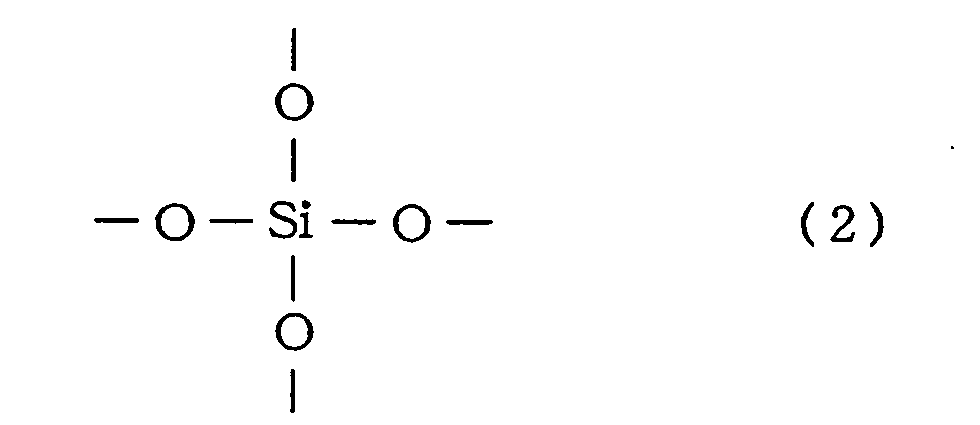
the alkenyl group content in said MQ resin ranges from 0.5 to 5wt%. The release sheet 3 can reduce concave defects on a convex-concave pattern transfer surface of the stamper receiving layer 2.
Description
- The present invention relates to a release sheet for stamper-receiving layer, on which a stamper-receiving layer to be used for producing an optical recording medium is laminated, and to an optical recording medium-producing sheet comprising the release sheet for stamper-receiving layer.
- In conventional optical recording medium manufacture, known methods for forming convex-concave shapes called pits or groove/lands, for information recording, include methods wherein a convex-concave pattern corresponding to the convex-concave shapes is transferred from a stamper having the convex-concave pattern to a constituent layer of the optical recording medium. As layers onto which the convex-concave pattern is transferred, stamper-receiving layers, wherein once the convex-concave pattern has been transferred thereto from the stamper, the layers are cured through irradiation of energy beams and the convex-concave pattern is fixed thereby, are studied. Optical recording medium-producing sheets having such stamper-receiving layers have ordinarily a structure wherein one or both faces of the stamper-receiving layer are protected by a release sheet.
- Patent document 1: Japanese Patent No.
3338660 - Patent document 2: Japanese Patent Application Laid-open No.
2002-25110 - The convex-concave pattern transferred to the stamper-receiving layer constitutes pits or groove/lands that are important for recording information in the optical recording medium. Therefore, there should be no irregularities, other than the convex-concave pattern, on the convex-concave pattern transfer surface of the stamper-receiving layer, with a view to achieve accurate reproduction of the recorded information.
- In conventional optical recording medium-producing sheets, however, concave-shaped defects (concave defects) having a diameter of about 500 µm may occur on the convex-concave pattern transfer surface of the cured stamper-receiving layer. Such concave defects on the convex-concave pattern transfer surface of the cured stamper-receiving layer may give rise to signal errors at portions where the concave defects are present, when the stamper-receiving layer is built into the optical recording medium.
- In the light of the above, it is an object of the present invention to provide a release sheet for stamper-receiving layers, and an optical recording medium-producing sheet, where concave defects are unlikely to occur in the convex-concave pattern transfer surface of the stamper-receiving layer.
- In order to achieve the above object, a first invention is a release sheet for stamper-receiving layer, on which a stamper-receiving layer to be used for producing an optical recording medium is laminated,
the release sheet comprising, on a side to which said stamper-receiving layer is laminated, a release agent layer,
wherein the release agent layer is formed using a release agent that contains an organopolysiloxane (other than an MQ resin below) containing an alkenyl group in the molecule, an MQ resin containing an alkenyl group and having, as constituent components, M units represented by formula (1)
R1 2R2-Si-O- .(1)
(where, R1 denotes an organic group and R2 denotes an alkenyl group), and Q units represented by formula (2)
the alkenyl group content in the MQ resin ranges from 0.5 to 5wt% (Invention 1). - The diameter of concave defects that appear in the convex-concave pattern transfer surface of conventional stamper-receiving layers is of about 500 µm. Therefore, these concave defects are believed to be caused by particles consisting of inorganic matter, for instance silica particles or the like, that are added to the release agent layer of a heavy release force type release sheet that is laminated on the convex-concave pattern transfer surface of the stamper-receiving layer. Thus, particles consisting of inorganic matter should not be added, but this would preclude obtaining heavy-release force, since the purpose of adding particles consisting of inorganic matter is to achieve heavy release. In the present invention (Invention 1), the alkenyl group content in the MQ resin is greater than usual, which allows increasing cross-linking density and achieving a desired release force, even when not using particles consisting of inorganic matter.
- The "optical recording medium" in the present description encompasses any medium where information can be recorded and reproduced optically. Although not limited thereto, such media include mainly reproduction-only, write-once or rewritable disk-like media (for instance, so called optical disks (including magnet-optical disks) such as CD, CD-ROM, CD-R, CD-RW, DVD, DVD-ROM, DVD-R, DVD-RW, DVD-RAM, LD, Blu-ray Disc, HD DVD and MO ).
- In the above invention (Invention 1), preferably, the alkenyl group content in the organopolysiloxane ranges from 0.1 to 3wt% (Invention 2).
- In the above inventions (
Inventions 1 and 2), preferably, the surface roughness (Ra) of the release agent layer is not greater than 0.05 µm, and the surface roughness (Rz) of the release agent layer is not greater than 4.0 µm (Invention 3). - In the above inventions (
Inventions 1 to 3), preferably, the release agent layer has a release force of 300 to 800 mN/50mm relative to the stamper-receiving layer before curing that is laminated on the release agent layer (Invention 4). - A second invention provides an optical recording medium-producing sheet comprising the above-mentioned release sheet (
Inventions 1 to 4) ; and an energy-beam curable stamper-receiving layer, laminated on the release agent layer of the release sheet, and having a storage elastic modulus before curing of 1×10³ to 1×10⁶ Pa (Invention 5). - A third invention provides an optical recording medium-producing sheet comprising a first above-mentioned release sheet (Invention 4) ; an energy-beam curable stamper-receiving layer, laminated on the release agent layer of the first release sheet, and having a storage elastic modulus before curing of 1×10³ to 1×10⁶ Pa; and a second release sheet, laminated on the stamper-receiving layer on an opposite side to the first release sheet, and having a release force of 50 to 200 mN/50mm relative to the stamper-receiving layer (Invention 6).
- The present invention allows suppressing the occurrence of concave defects, caused by the release sheet, on the convex-concave pattern transfer surface of the stamper-receiving layer, while achieving a desired release force in the release sheet.
-
-
Fig. 1 is a cross-sectional diagram of an optical recording medium-producing sheet according to an embodiment of the present invention; and -
Fig. 2 is a diagram illustrating an example of method for producing an optical recording medium using the optical recording medium-producing sheet according to the embodiment. -
- 1 optical recording medium-producing sheet
- 2 stamper-receiving layer
- 3 heavy release force type release sheet
- 31 base material
- 32 release agent layer
- 4 light release force type release sheet
- 41 base material
- 42 release agent layer
- Hereinafter, an embodiment of the present invention will be explained.
Fig. 1 is a cross-sectional diagram of an optical recording medium-producing sheet according to an embodiment of the present invention. As illustrated inFig. 1 , an optical recording medium-producingsheet 1 according to the present embodiment comprises a stamper-receivinglayer 2, a heavy release forcetype release sheet 3 laminated on the face of the stamper-receivinglayer 2 where a convex-concave pattern is to be transferred (lower face inFig. 1 ), and a light release forcetype release sheet 4 laminated on the other face of the stamper-receiving layer 2 (upper face inFig. 1 ). - The heavy release force
type release sheet 3 comprises abase material 31, and arelease agent layer 32 formed on the face of thebase material 31 on a side to which the stamper-receivinglayer 2 is laminated. - The
base material 31 of the heavy release forcetype release sheet 3 is not particularly limited, and may be appropriately selected from among any base materials used in conventional release sheets. Examples of such abase material 31 include resin films, for instance, polyester films such as polyethylene terephthalate or polyethylene naphthalate films; polyolefin films such as polypropylene or polymethylpentene films; or polycarbonate films, polyvinyl acetate films or the like. - The thickness of the
base material 31 is not particularly limited, but ranges ordinarily from about 10 to about 200 µm, preferably from about 25 to about 75 µm. - The
release agent layer 32 of the heavy release forcetype release sheet 3 is a layer formed using a heavy release force type release agent (hereafter, "release agent H"). The release agent H contains at least an organopolysiloxane (A) as a base polymer, an MQ resin (B) and a cross-linking agent (C), and does not substantially contain particles consisting of inorganic matter (for instance silica particles). Such substantial absence of particles consisting of inorganic matter allows preventing the particles from forming protrusions on therelease agent layer 32, and allows enhancing the smoothness of the surface of therelease agent layer 32. In turn, this allows suppressing the occurrence of concave defects in the convex-concave pattern transfer surface of the stamper-receivinglayer 2 that is closely touched to therelease agent layer 32. - The organopolysiloxane (A) is an organopolysiloxane containing an alkenyl group in the molecule, other than the below-described MQ resin (B). As the organopolysiloxane (A) there is preferably used a diorganopolysiloxane having, as a main structural unit, the bifunctional structural unit (D unit) represented by formula (3).

- In formula (3), R3 denotes a substituted or unsubstituted C1 to C20, preferably C1 to C12 alkyl group or aryl group, for instance an alkyl group such as a methyl group, ethyl group, propyl group or butyl group; a cycloalkyl group such as a cyclohexyl group; an aryl group such as a phenyl group or tolyl group; or a chloromethyl group, a trifluoropropyl group, a cyanoethyl group or the like resulting from substituting some or all the hydrogen atoms of the foregoing groups with a halogen atom, a cyano group or the like. Industrially preferred among the above groups is a methyl group or phenyl group.
- Meanwhile, R4 is the same functional group as R3, or is selected from among a preferably C2 to C8 alkenyl group such as a vinyl group, allyl group or propenyl group, a C1 to C8 alkoxy group such as a methoxy group, ethoxy group, propoxy group or methoxyethoxy group, or hydroxyl group or epoxy group. Industrially preferred among the foregoing are methyl, phenyl or vinyl groups. R3 and R4 may be identical or dissimilar.
- The O (oxygen atom) in formula (3) forms siloxane bonds shared by adjacent structural units.
- Preferably, the ends of the above-described diorganopolysiloxane are capped by hydroxyl groups or by monofunctional structural units represented by formula (4) and that share an oxygen atom
(R3-)n(R4-)3-nSi-O- (4)
(In formula (4), R3 and R4 may be the same as above, but preferably R3 is a methyl group or phenyl group, and R4 is a methyl group, phenyl group or vinyl group. n is an integer from 1 to 3). - The above-described diorganopolysiloxane has essentially a linear structure, but may also have a branched structure partially comprising trifunctional structural units (T units) represented by formula (5) and/or tetrafunctional structural units (Q units) represented by formula (2).

- In formula (3) and formula (5), a predetermined proportion of R4 must be an alkenyl group, preferably, in particular, a vinyl group. The alkenyl group content in the organopolysiloxane (A) ranges preferably from 0.1 to 3wt%, in particular from 0.5 to 2.5wt%. When the alkenyl group content is smaller than 0.1wt%, cross-linking density cannot be sufficiently increased, which may preclude obtaining a desired release force in the formed
release agent layer 32. On the other hand, the cross-linking density becomes excessive when the content of alkenyl group is greater than 3wt%, which may preclude obtaining a desired release force in the formedrelease agent layer 32. - The average degree of polymerization of the organopolysiloxane (A) ranges preferably from 2000 to 7000, in particular from 3000 to 6000.
- The MQ resin (B) comprises, as constituent components, monofunctional structural units (M units) represented by formula (1)
R1 2R2-Si-O- (1)
and tetrafunctional structural units (Q units) represented by formula (2)
- In formula (1), R1 denotes an organic group and R2 an alkenyl group. Preferably, the organic group of R1 is a C1 to C20, preferably a C1 to C12 substituted or unsubstituted alkyl group or aryl group, for instance an alkyl group such as a methyl group, ethyl group, propyl group or butyl group; a cycloalkyl group such as a cyclohexyl group; an aryl group such as a phenyl group or tolyl group; or a chloromethyl group, a trifluoropropyl group, a cyanoethyl group or the like resulting from substituting some or all the hydrogen atoms of the foregoing groups with a halogen atom, a cyano group or the like; in industrial terms, R1 is preferably a methyl group or phenyl group.
- Examples of the alkenyl group include, for instance, a vinyl group, allyl group, methacryl group, hexenyl group, butadienyl group, hexadienyl group, cyclopentenyl group, cyclopentadienyl group, cyclohexenyl group or the like, preferably, in particular, vinyl group.
- The O (oxygen atom) in formula (1) and formula (2) forms siloxane bonds shared by adjacent structural units.
- Preferably, the ends of the MQ resin (B) are capped by hydroxyl groups or by monofunctional structural units, represented by formula (4), that share an oxygen atom.
- Besides those represented by formula (1), the M units of the MQ resin (B) may be also units in which R2 in formula (1) is the same organic group as R1 (R1 and R2 may be identical or dissimilar).
- Fundamentally, the MQ resin (B) comprises only M units represented by formula (1) and Q units represented by formula (2), but may also partially comprise D units represented by formula (3) and/or T units represented by formula (5).
- The alkenyl group content in the MQ resin (B) ranges preferably from 0.5 to 5wt%, in particular from 1 to 4wt%. When the alkenyl group content is smaller than 0.5wt%, cross-linking density cannot be sufficiently increased, which may preclude obtaining a desired release force in the formed
release agent layer 32. On the other hand, cross-linking density becomes excessive when the content of alkenyl group is greater than 5wt%, which may preclude obtaining a desired release force in the formedrelease agent layer 32. - The weight-average molecular weight of the MQ resin (B) ranges preferably from 1000 to 7000, in particular from 2000 to 6000.
- The blending amount of the MQ resin (B) ranges preferably from 30 to 90 parts by weight, in particular from 40 to 80 parts by weight, relative to 100 parts by weight of the organopolysiloxane (A). When the blending amount of the MQ resin (B) is smaller than 30 parts by weight, cross-linking density cannot be sufficiently increased, which may preclude obtaining a desired release force in the formed
release agent layer 32. On the other hand, when the blending amount of the MQ resin (B) is greater than 90 parts by weight, the cross-linking density becomes excessive, which may preclude obtaining a desired release force in the formedrelease agent layer 32. - As the cross-linking agent (C) there can be used, for instance, a polyorganosiloxane having at least two hydrogen atoms bonded to silicon atoms in the molecule. Specific examples thereof include silicone resins such as a dimethylhydrogensiloxy end-capped dimethylsiloxane-methylhydrogensiloxane copolymer, a trimethylsiloxy end-capped dimethylsiloxane-methylhydrogensiloxane copolymer, a trimethylsiloxyend-cappedpoly(methylhydrogensiloxane), or a poly (hydrogen silsesquioxane). The usage amount of the cross-linking agent ranges ordinarily from 0.1 to 100 parts by weight, preferably from 0.3 to 50 parts by weight, relative to a total 100 parts by weight of organopolysiloxane (A) and MQ resin (B).
- Besides the components (A) to (C) above, the release agent H may optionally contain a catalyst, an addition reaction inhibitor and the like. The catalyst used may be an ordinary platinum-group compound. Examples of platinum-group compounds include, for instance, platinum chloride complexes, chloroplatinic acid, alcohol-modified chloroplatinic acid, olefin complexes of chloroplatinic acid, as well as palladium or rhodium catalysts. The usage amount of the catalyst ranges from about 0.1 to about 5 parts by weight relative to the total weight of the organopolysiloxane (A), the MQ resin (B) and the cross-linking agent (C).
- The addition reaction inhibitor is a component used for imparting storage stability at room temperature to the organopolysiloxane (A) and the MQ resin (B) when an addition reaction is utilized to. Specific examples of the addition reaction inhibitor include, for instance, 3,5-dimethyl-1-hexin-3-ol, 3-methyl-1-penten-3-ol, 3-methyl-3-penten-1-yne, 3,5-dimethyl-3-hexen-1-yne, tetravinyl siloxane rings, benzotriazole or the like. The usage amount of the addition reaction inhibitor ranges ordinarily from 0.01 to 20 parts by weight, preferably from 0.1 to 15 parts by weight relative to a total 100 parts by weight of the organopolysiloxane (A), the MQ resin (B) and the cross-linking agent (C).
- To form the
release agent layer 32 on thebase material 31, the various components of the release agent H are blended first at their predetermined ratios to prepare a coating solution having a viscosity that allows coating. The organic solvent used herein is not particularly limited, and various solvents may be used, for instance a hydrocarbon compound such as toluene, hexane or heptane, as well as ethyl acetate, methyl ethyl ketone or mixtures of the foregoing. - The coating solution thus prepared is coated onto the surface of the
base material 31 by, for instance, gravure coating, bar coating, spray coating or the like. The solids-basis coating amount is appropriately adjusted so as to range ordinarily from 0.01 to 3.0 g/m2, preferably from 0.02 to 1.5 g/m2. Application of the coating solution is followed by drying, heating, UV irradiation or the like, to cure the release agent H and yield thereby therelease agent layer 32. - The thickness of the
release agent layer 32 ranges preferably from 0.03 to 0.2 µm, in particular from 0.05 to 0.15 µm. - The
release agent layer 32 exhibits excellent surface smoothness, since it is formed using the release agent H, which does not substantially contain particles consisting of inorganic matter. Specifically, it is possible to form arelease agent layer 32 having a surface roughness (Ra) no greater than 0.05 µm and a surface roughness (Rz) no greater than 4.0 µm. - Such surface roughness in the
release agent layer 32 allows suppressing the occurrence of concave defects in the convex-concave pattern transfer surface of the stamper-receivinglayer 2 that is closely touched to therelease agent layer 32. Specifically, the frequency of occurrence of concave defects having diameters of 100 µm or greater in the convex-concave pattern transfer surface of the stamper-receiving layer 2 (after drying, before curing) can be kept at no more than 0.5 defects/m2. - The
release agent layer 32 is formed using an MQ resin having a greater alkenyl group content than usual. This allows, as a result, increasing cross-linking density and achieving greater release force. Specifically, there can be formed a heavy release force typerelease agent layer 32 having a release force of 300 to 800 mN/50mm, in particular 300 to 600 mN/50mm, relative to the stamper-receivinglayer 2 before curing that is laminated on therelease agent layer 32. - As described above, the silicone resin that makes up the
release agent layer 32 has high cross-linking density. This allows suppressing the amount of silicone being transferred to the stamper-receivinglayer 2 that is laminated on therelease agent layer 32. Specifically, the amount of silicone being transferred to the convex-concave pattern transfer surface of the stamper-receiving layer 2 (after drying, before curing) can be kept no greater than 2.0Atom%. Suppressing thus the silicone transfer amount allows reliably forming a reflective film on the convex-concave pattern transfer surface of the stamper-receivinglayer 2. - The stamper-receiving
layer 2, onto which the convex-concave pattern formed on the stamper is transferred, is a layer comprising pits or groove/lands. The stamper-receivinglayer 2 contains, as a main component, a polymer material having energy-beam curability, preferably, an acrylate copolymer having energy-beam curable groups in the side chains, in particular, an energy-beam curable copolymer having a molecular weight not lower than 100,000 and having energy-beam curable groups in the side chains, obtained through reaction of an acrylic copolymer having monomer units that contain a functional group, and a compound containing unsaturated groups having substituents that bond to the functional group. In addition, the stamper-receivinglayer 2 contains optionally a photopolymerization initiator, a polymer component or oligomer component lacking energy-beam curability, an energy-beam curable polyfunctional monomer or oligomer component, a cross-linking agent, as well as other additives (UV absorbents, plasticizers, fillers, antioxidants, tackifiers, pigments, dyes, coupling agents or the like). - The storage elastic modulus of the stamper-receiving
layer 2 before curing ranges preferably from 1×10³ to 1×10⁶ Pa, in particular from 1×10⁴ to 5×10⁵ Pa. The measurement temperature of the "storage elastic modulus before curing" is a temperature identical to that of the work environment where the stamper is superposed (pressed) against the optical recording medium-producingsheet 1. That is, when the stamper and the optical recording medium-producingsheet 1 are superposed at room temperature, the storage elastic modulus is measured at room temperature, and when the stamper and the optical recording medium-producingsheet 1 are superposed under heating, the storage elastic modulus is measured at the same temperature as the heating temperature. - When the storage elastic modulus of the stamper-receiving
layer 2 before curing is kept within the above ranges, the convex-concave pattern formed on the stamper is transferred precisely to the stamper-receivinglayer 2 by merely pressing the stamper against the stamper-receivinglayer 2. This makes optical disk manufacture extremely simple. - The storage elastic modulus of the stamper-receiving
layer 2 after curing is preferably not smaller than 1×10⁷ Pa, and in particular, ranges from 1×10⁸ to 1×10¹¹ Pa. The measurement temperature of the "storage elastic modulus after curing" is set at the same temperature as that of the storage environment of the optical disk, i.e. at room temperature. - When the storage elastic modulus of the stamper-receiving
layer 2 after curing is kept within the above range, the pits or groove/lands transferred to the stamper-receivinglayer 2 become reliably fixed through curing. This allays the concern of breakage and/or deformation of the pits or groove/lands during separation of the stamper and the stamper-receivinglayer 2. - The thickness of the stamper-receiving
layer 2 is determined in accordance with the depth of the pits or grooves to be formed, but ranges ordinarily from about 5 to about 100 µm, preferably from about 5 to about 50 µm. - The light release force
type release sheet 4 comprises abase material 41 and arelease agent layer 42 formed on the face of thebase material 41 onto which the stamper-receivinglayer 2 is laminated. - The
base material 41 of the light release forcetype release sheet 4 is not particularly limited, and the base materials that are exemplified above as thebase material 31 of heavy release forcetype release sheet 3 may be used as thebase material 41. - The
release agent layer 42 of the light release forcetype release sheet 4 is a layer formed using a light release force type release agent. So long as therelease agent layer 42 has a desired release force, the light release force type release agent used is not particularly limited, and may be, for instance, a silicone resin, a fluororesin, an alkyd resin, a long-chain alkyl resin or the like. Preferably, the release agent has a silicone resin as a main component. The release force of therelease agent layer 42 ranges preferably from 50 to 200 mN/50mm, in particular from 50 to 150 mN/50mm. - The light release force
type release sheet 4 can be produced in accordance with the same method as the above-described heavy release forcetype release sheet 3. - To manufacture the optical recording medium-producing
sheet 1 according to the present embodiment there may be prepared a coating solution of the material that makes up the stamper-receivinglayer 2, the coating solution being then coated, by, for instance, gravure coating, bar coating or spray coating, onto one of the release sheets, ordinarily onto therelease agent layer 32 of the heavy release forcetype release sheet 3, followed by drying, to form the stamper-receivinglayer 2. Thereafter, the other release sheet, ordinarily therelease agent layer 42 of the light release forcetype release sheet 4, may be laminated onto the surface of the stamper-receivinglayer 2 in such a manner that therelease agent layer 42 is in contact with the stamper-receivinglayer 2. - With reference to
Fig. 2 , an explanation follows next on an example of a method for producing an optical recording medium using the above-described optical recording medium-producingsheet 1. - Firstly, the light release force
type release sheet 4 of the optical recording medium-producingsheet 1 is peeled off, to expose one of the faces of the stamper-receivinglayer 2, as illustrated inFig. 2(a) . The stamper-receivinglayer 2 can be prevented from peeling off the heavy release forcetype release sheet 3 because of the release force difference of the light release forcetype release sheet 4 and the heavy release forcetype release sheet 3 relative to the stamper-receivinglayer 2. - Next, the exposed stamper-receiving
layer 2 is laminated and pressure-bonded onto an opticalrecording medium substrate 5 made of polycarbonate, as illustrated inFig. 2(b) . The heavy release forcetype release sheet 3 laminated on the stamper-receivinglayer 2 is peeled off, to expose the convex-concave pattern transfer surface of the stamper-receivinglayer 2, as illustrated inFig. 2(c) . - Next, a stamper S is pressed against the surface of the exposed stamper-receiving
layer 2, to transfer the convex-concave pattern of the stamper S to the stamper-receivinglayer 2, as illustrated inFig. 2(d) . With the stamper S closely touched to the stamper-receivinglayer 2, energy beams are irradiated to the stamper-receivinglayer 2, using an energy beam irradiation apparatus (for instance, an UV lamp L inFig. 2 ), from the side of the opticalrecording medium substrate 5, as illustrated inFig. 2(e) . The stamper-receivinglayer 2 is cured thereby, with an accompanying increase in storage elastic modulus. - Thereafter, the stamper S is removed off the stamper-receiving
layer 2, as illustrated inFig. 2(e) . Pits or groove/lands are formed thus on the stamper-receivinglayer 2 through transfer/fixing of the convex-concave pattern of the stamper S. Therelease agent layer 32 of the heavy release forcetype release sheet 3 closely touched to the stamper-receivinglayer 2 is formed using a release agent not substantially containing inorganic matter particles. This has the effect of preventing formation of concave defects, caused by such particles, on the convex-concave pattern transfer surface of the stamper-receivinglayer 2. - Next, a
reflective film 6 is formed, by sputtering or the like, on the convex-concave pattern transfer surface of the stamper-receivinglayer 2, as illustrated inFig. 2(f) . Thereflective film 6 may be a multilayer film further comprising a recording layer such as a phase-change recording layer. - Lastly, a
cover sheet 8 is laminated on thereflective film 6, with an adhesive 7 interposed in between, as illustrated inFig. 2 (g) , to yield an optical recordingmedium. The optical recording medium thus obtained does not substantially have concave defects on the convex-concave pattern transfer surface of the stamper-receivinglayer 2. This prevents the occurrence of signal errors caused by such concave defects. - The embodiments explained above are described to facilitate understanding of the present invention and is not to limit the present invention. Accordingly, respective elements disclosed in the above embodiments include all design modifications and equivalents belonging to the technical scope of the present invention.
- Following is a more detailed description of the present invention through examples and so on; however, the scope of the present invention is not limited by these examples and so on.
- A release agent coating solution having a 1.5wt% solids concentration was obtained by mixing, and diluting in a mixed solvent of toluene/MEK, 100 parts by weight of a mixture (BY24-567, by Dow Corning Toray Co.,Ltd., solids 41wt%, containing 60 parts by weight of MQ resin having vinyl groups relative to 100 parts by weight of dimethylpolysiloxane having vinyl groups) of dimethylpolysiloxane having vinyl groups (vinyl group content: 1.5wt%, average degree of polymerization: 4500), polymethylhydrogensiloxane, and an MQ resin having vinyl groups (vinyl group content in the MQ resin: 2.0wt%, weight-average molecular weight: 4000) ; 9. 5 parts by weight of a reaction inhibitor (BY24-808, by Dow Corning Toray Co.,Ltd., solids 20wt%); and 2.5 parts by weight of a platinum catalyst (CAT-BY24-835, by Dow Corning Toray Co.,Ltd., solids 100wt%). A 38 µm-thick polyethylene terephthalate film (T-100, by Mitsubishi Chemical polyester film) was prepared then as the base material. The release agent coating solution was uniformly coated onto the base material to a coating thickness of 0.1 µm, and was cured in a thermal treatment at 140°C, to yield a release sheet which a release agent layer was formed on one face of the base material.
- An acrylate copolymer solution A (solids concentration 35wt%) having a weight-average molecular weight of 850,000 was obtained by reacting 80 parts by weight of n-butyl acrylate with 20 parts by weight of acrylic acid in a mixed solvent of ethyl acetate and methyl ethyl ketone (weight ratio 50:50). In 35 parts by weight (solids) of the obtained acrylate copolymer solution A there were dissolved 2.5 parts by weight of 2,2-dimethoxy-1,2-diphenylethan-1-one (Irgacure 651, by Ciba Specialty Chemicals) as a photopolymerization initiator; 28 parts by weight of a composition comprising energy beam-curable polyfunctional monomers and oligomers (KAYARAD NKR-001, made by Nippon Kayaku Co., Ltd.); 7 parts by weight of an energy-beam curable urethane acrylate compound (Shiko UV-6020EA, by Nippon Synthetic Chemical Industry Co., Ltd.); and 0.5 parts by weight of a cross-linking agent comprising a polyisocyanate compound (Oribain BHS-8515, by Toyo Ink Mfg. Co., Ltd.); the solids concentration of the resulting solution was adjusted to 40wt%, to yield a coating agent for stamper-receiving layer.
- The obtained coating agent for stamper-receiving layer was coated by knife coater (28.5 g/m2) onto the release agent layer of the heavy release force type release sheet, and was dried for 1 minute at 90°C, to form a 25 µm-thick stamper-receiving layer. To prepare an optical recording medium-producing sheet, a release sheet (SP-PET38GS, by LINTEC Corporation), as a light release force type release sheet, obtained by subjecting one face of a 38 µm-thick polyethylene terephthalate film to a release treatment with a light release force type silicone resin, was laminated on the surface of the stamper-receiving layer.
- A release agent coating solution having a 1.5wt% solids concentration was obtained by mixing, and diluting in a mixed solvent of toluene/MEK, 50 parts by weight of a mixture (BY24-510, by Dow Corning Toray Co.,Ltd., solids 30wt%) of dimethylpolysiloxane having vinyl groups and polymethylhydrogensiloxane; 50 parts by weight of a mixture (BY24-562, by Dow Corning Toray Co.,Ltd., solids 30wt%) of silica and an MQ resin having vinyl groups (vinyl group content in the MQ resin: 2.0wt%); 5.0 parts by weight of a reaction inhibitor (BY24-808 by Dow Corning Toray Co.,Ltd., solids 20wt%); and 2.0 parts by weight of a platinum catalyst (CAT-BY24-835 by Dow Corning Toray Co.,Ltd.). A 38 µm-thick polyethylene terephthalate film (T-100, by Mitsubishi Chemical polyester film) was prepared then as the base material. The release agent coating solution was uniformly coated onto the base material to a coating thickness of 0.1 µm, and was cured in a thermal treatment at 140°C, to yield a release sheet which a release agent layer was formed on one face of the base material.
- An optical recording medium-producing sheet was produced in the similar way as in Example 1 but using herein the heavy release force type release sheet obtained above.
- The surface roughness (Ra) and surface roughness (Rz) of the release agent layers of the heavy release force type release sheets obtained in the example and comparative example were measured using a surface roughness meter (SVP-3000S4 by Mitutoyo CORPORATION). The results are given in Table 1.
- The release force of the light release force type release sheet from the stamper-receiving layer and the release force of the heavy release force type release sheet from the stamper-receiving layer were measured for the optical recording medium-producing sheets obtained in the example and comparative example. The results are given in Table 1.
- The optical recording medium-producing sheets obtained in the example and comparative example were left to stand for 1 day in an environment at a temperature of 23°C and 50% humidity, after which samples 50 mm wide and 200 mm long were cut out of the sheets. The heavy release force
type release sheet 3 was fixed to a mount, and then the release force of the light release force type release sheet was measured using a tensile tester with which the light release force type release sheet was pulled in the 180° direction at a peeling speed of 0.3 m/minute. - To measure the release force of the heavy release force type release sheets, the light release force type release sheets were removed from the optical recording medium-producing sheets obtained in the example and comparative example, and a 50 µm-thickpolyethylene terephthalate film was stuck to the exposed surface of the stamper-receiving layer. The sheets were left to stand for 1 day in an environment at a temperature of 23°C and 50% humidity, after which samples 50 mm wide and 200 mm long were cut out. The stuck polyethylene terephthalate film was fixed to a mount, and then the release force of the heavy release force type release sheet was measured using a tensile tester with which the heavy release force type release sheet was pulled in the 180° direction at a peeling speed of 0.3 m/minute.
- The heavy release force type release sheet was peeled off the stamper-receiving layer in the optical recording medium-producing sheets obtained in the example and comparative example. The number of concave defects on the surface of the exposed stamper-receiving layers was measured using a defect analyzer (B-LSC-5790-LA, by Mec Co.). The samples were 1000 mm wide × 250 m long. The results are given in Table 2.
- The heavy release force type release sheet was peeled off the stamper-receiving layer in the optical recording medium-producing sheets obtained in the example and comparative example. The silicone transfer amount at the surface of the exposed stamper-receiving layers was measured by scanning X-ray photoelectron spectroscopy (using a PHI Quantera SXM, by Ulvac Phi) (measured elements: silicon (Si) and carbon (C)). The silicone transfer amount, obtained as the value Si/(Si+C)times 100, is expressed in "Atom%". The results are given in Table 1.
-
[Table 1] Example 1 Comparative example 1 Surface roughness (Ra) (µm) 0.047 0.057 Surface roughness (Rz) (µm) 2.99 4.35 Release force of light release force type release sheet (mN/50mm) 135 135 Release force of heavy release force type release sheet (mN/50mm) 450 480 Silicone transfer amount (Atom%) 1.18 8.42 -
[Table 2] Size (mm) Example 1 Comparative example 1 Defect count
(defects)(defects/m2) Defect count
(defects)(defects/m2) 0.1 to 0.3 61 0.15 114 0.49 0.3 to 0.5 23 0.06 52 0.22 ≥ 0.5 3 0.01 13 0.06 Total 87 0.22 179 0.77 - Table 1 and Table 2 show a significant reduction in the number of concave defects in the stamper-receiving layer, and an extremely small amount of silicone transfer, when using the heavy release force type release sheet produced in the example.
- The present invention is useful for producing signal error-free optical recording media with good yield.
Claims (6)
- A release sheet for stamper-receiving layer, on which a stamper-receiving layer to be used for producing an optical recording medium is laminated,
the release sheet comprising, on a side to which said stamper-receiving layer is laminated, a release agent layer,
wherein said release agent layer is formed using a release agent that contains an organopolysiloxane (other than an MQ resin below) containing an alkenyl group in the molecule, an MQ resin containing an alkenyl group and having, as constituent components, M units represented by formula (1)
R1 2R2-Si-O- (1)
(where, R1 denotes an organic group and R2 denotes an alkenyl group), and Q units represented by formula (2)
the alkenyl group content in said MQ resin ranges from 0.5 to 5wt%. - The release sheet for stamper-receiving layers according to claim 1, wherein the alkenyl group content in said organopolysiloxane ranges from 0.1 to 3wt%.
- The release sheet for stamper-receiving layers according to claim 1 or 2, wherein the surface roughness (Ra) of said release agent layer is not greater than 0.05 µm, and the surface roughness (Rz) of said release agent layer is not greater than 4.0 µm.
- The release sheet for stamper-receiving layer according to any of claims 1 to 3, wherein said release agent layer has a release force of 300 to 800 mN/50mm relative to the stamper-receiving layer before curing that is laminated on said release agent layer.
- An optical recording medium-producing sheet, comprising:the release sheet according to any of claims 1 to 4; andan energy-beam curable stamper-receiving layer, laminated on the release agent layer of said release sheet, and having a storage elastic modulus before curing of 1×10³ to 1×10⁶ Pa.
- An optical recording medium-producing sheet, comprising:a first release sheet according to claim 4;an energy-beam curable stamper-receiving layer, laminated on the release agent layer of said first release sheet, and having a storage elastic modulus before curing of 1×10³ to 1×10⁶ Pa; anda second release sheet, laminated on said stamper-receiving layer on an opposite side to said first release sheet, and having a release force of 50 to 200 mN/50mm relative to said stamper-receiving layer.
Applications Claiming Priority (2)
| Application Number | Priority Date | Filing Date | Title |
|---|---|---|---|
| JP2007092158 | 2007-03-30 | ||
| PCT/JP2008/053991 WO2008126524A1 (en) | 2007-03-30 | 2008-03-05 | Peelable sheet for stamper receiving layer, and sheet for production of optical recording medium |
Publications (3)
| Publication Number | Publication Date |
|---|---|
| EP2133877A1 true EP2133877A1 (en) | 2009-12-16 |
| EP2133877A4 EP2133877A4 (en) | 2012-01-04 |
| EP2133877B1 EP2133877B1 (en) | 2012-12-19 |
Family
ID=39863682
Family Applications (1)
| Application Number | Title | Priority Date | Filing Date |
|---|---|---|---|
| EP20080721411 Not-in-force EP2133877B1 (en) | 2007-03-30 | 2008-03-05 | Peelable sheet for stamper receiving layer, and sheet for production of optical recording medium |
Country Status (6)
| Country | Link |
|---|---|
| US (1) | US8409684B2 (en) |
| EP (1) | EP2133877B1 (en) |
| JP (1) | JP5419277B2 (en) |
| KR (1) | KR101481392B1 (en) |
| TW (1) | TWI424432B (en) |
| WO (1) | WO2008126524A1 (en) |
Cited By (1)
| Publication number | Priority date | Publication date | Assignee | Title |
|---|---|---|---|---|
| WO2011002604A1 (en) * | 2009-07-02 | 2011-01-06 | Brady Worldwide, Inc. | Silicone optical film with release layers |
Families Citing this family (1)
| Publication number | Priority date | Publication date | Assignee | Title |
|---|---|---|---|---|
| JP5171332B2 (en) * | 2008-03-18 | 2013-03-27 | リンテック株式会社 | Release sheet, polarizing plate with release sheet, and substrate-less double-sided adhesive sheet |
Family Cites Families (7)
| Publication number | Priority date | Publication date | Assignee | Title |
|---|---|---|---|---|
| GB9322794D0 (en) * | 1993-11-05 | 1993-12-22 | Dow Corning | Silicone release compositions |
| JP3338660B2 (en) | 1998-01-21 | 2002-10-28 | ソニー株式会社 | optical disk |
| JP2002025110A (en) | 2000-07-13 | 2002-01-25 | Bridgestone Corp | Recording medium |
| JP4359411B2 (en) * | 2001-10-09 | 2009-11-04 | リンテック株式会社 | Optical disc manufacturing sheet |
| JP3989755B2 (en) * | 2002-03-18 | 2007-10-10 | リンテック株式会社 | Optical disc manufacturing sheet |
| JP2005255706A (en) * | 2004-03-09 | 2005-09-22 | Lintec Corp | Hardenable pressure-sensitive adhesive composition, sheet for manufacturing optical disc and optical disc |
| JP4764173B2 (en) * | 2006-01-16 | 2011-08-31 | 株式会社ブリヂストン | Photocurable transfer sheet, method for producing optical information recording medium using the same, and optical information recording medium |
-
2008
- 2008-03-05 JP JP2009508977A patent/JP5419277B2/en not_active Expired - Fee Related
- 2008-03-05 EP EP20080721411 patent/EP2133877B1/en not_active Not-in-force
- 2008-03-05 KR KR1020097019325A patent/KR101481392B1/en not_active Expired - Fee Related
- 2008-03-05 WO PCT/JP2008/053991 patent/WO2008126524A1/en not_active Ceased
- 2008-03-05 US US12/450,179 patent/US8409684B2/en not_active Expired - Fee Related
- 2008-03-12 TW TW97108681A patent/TWI424432B/en not_active IP Right Cessation
Cited By (1)
| Publication number | Priority date | Publication date | Assignee | Title |
|---|---|---|---|---|
| WO2011002604A1 (en) * | 2009-07-02 | 2011-01-06 | Brady Worldwide, Inc. | Silicone optical film with release layers |
Also Published As
| Publication number | Publication date |
|---|---|
| EP2133877A4 (en) | 2012-01-04 |
| KR101481392B1 (en) | 2015-01-12 |
| EP2133877B1 (en) | 2012-12-19 |
| TW200849242A (en) | 2008-12-16 |
| TWI424432B (en) | 2014-01-21 |
| JPWO2008126524A1 (en) | 2010-07-22 |
| JP5419277B2 (en) | 2014-02-19 |
| US20100040822A1 (en) | 2010-02-18 |
| US8409684B2 (en) | 2013-04-02 |
| KR20090123886A (en) | 2009-12-02 |
| WO2008126524A1 (en) | 2008-10-23 |
Similar Documents
| Publication | Publication Date | Title |
|---|---|---|
| CN100401401C (en) | optical information medium | |
| EP1835001A1 (en) | Composition for coating, hard coat film and optical recording medium | |
| KR20050041899A (en) | Coating composition, hard coat film and optical disk | |
| EP1469466B1 (en) | Optical recording medium-producing sheet and optical recording medium | |
| EP1626395B1 (en) | Coating composition, coating film, method of manufacturing coating film, and optical recording medium | |
| US5151310A (en) | Information recording medium | |
| US20080226889A1 (en) | Curable compositions | |
| EP2133877B1 (en) | Peelable sheet for stamper receiving layer, and sheet for production of optical recording medium | |
| KR20120112027A (en) | Sheet for manufacturing multi-layer optical record media, multi-layer structure for optical record media and multi-layer optical structure | |
| JP4033224B2 (en) | Ultraviolet curable resin composition and optical information recording medium | |
| JP3989755B2 (en) | Optical disc manufacturing sheet | |
| TWI419929B (en) | Ultraviolet curable resin composition and optical information recording media | |
| JP2008044237A (en) | Release agent, method for forming concave / convex pattern using the same, method for producing optical information recording medium, and optical information recording medium | |
| JP2006048798A (en) | Sheet for forming protective layer of optical recording medium, optical recording medium and manufacturing method of those | |
| JPWO2008111312A1 (en) | Multilayer information recording medium manufacturing method, signal transfer substrate and manufacturing method thereof | |
| JP4658858B2 (en) | Photocurable transfer sheet, method for producing optical information recording medium using the same, and optical information recording medium | |
| JP2003338089A (en) | Optical information recording medium | |
| JP2006236518A (en) | Sheet for protective layer formation of optical recording medium, optical recording medium and manufacturing method of those | |
| JP2006277809A (en) | Surface protecting film for polycarbonate | |
| JP2006035733A (en) | Surface protective film, surface protective laminate, and method for producing surface protective laminate | |
| JP2518954C (en) | ||
| JP3975806B2 (en) | Photosensitive element for optical disk spacer formation and optical disk | |
| JP4244823B2 (en) | Ultraviolet curable composition for optical disc, optical disc using the composition, and production method | |
| JP2007149229A (en) | Energy ray curing resin composition for stamper receiving layer, sheet for manufacturing optical recording medium and optical recording medium |
Legal Events
| Date | Code | Title | Description |
|---|---|---|---|
| PUAI | Public reference made under article 153(3) epc to a published international application that has entered the european phase |
Free format text: ORIGINAL CODE: 0009012 |
|
| 17P | Request for examination filed |
Effective date: 20091006 |
|
| AK | Designated contracting states |
Kind code of ref document: A1 Designated state(s): AT BE BG CH CY CZ DE DK EE ES FI FR GB GR HR HU IE IS IT LI LT LU LV MC MT NL NO PL PT RO SE SI SK TR |
|
| DAX | Request for extension of the european patent (deleted) | ||
| A4 | Supplementary search report drawn up and despatched |
Effective date: 20111207 |
|
| RIC1 | Information provided on ipc code assigned before grant |
Ipc: G11B 7/26 20060101ALI20111201BHEP Ipc: G11B 7/257 20060101AFI20111201BHEP |
|
| GRAP | Despatch of communication of intention to grant a patent |
Free format text: ORIGINAL CODE: EPIDOSNIGR1 |
|
| GRAS | Grant fee paid |
Free format text: ORIGINAL CODE: EPIDOSNIGR3 |
|
| GRAA | (expected) grant |
Free format text: ORIGINAL CODE: 0009210 |
|
| AK | Designated contracting states |
Kind code of ref document: B1 Designated state(s): AT BE BG CH CY CZ DE DK EE ES FI FR GB GR HR HU IE IS IT LI LT LU LV MC MT NL NO PL PT RO SE SI SK TR |
|
| REG | Reference to a national code |
Ref country code: GB Ref legal event code: FG4D |
|
| REG | Reference to a national code |
Ref country code: CH Ref legal event code: EP |
|
| REG | Reference to a national code |
Ref country code: AT Ref legal event code: REF Ref document number: 589751 Country of ref document: AT Kind code of ref document: T Effective date: 20130115 |
|
| REG | Reference to a national code |
Ref country code: DE Ref legal event code: R096 Ref document number: 602008020953 Country of ref document: DE Effective date: 20130207 |
|
| REG | Reference to a national code |
Ref country code: NL Ref legal event code: T3 |
|
| PG25 | Lapsed in a contracting state [announced via postgrant information from national office to epo] |
Ref country code: FI Free format text: LAPSE BECAUSE OF FAILURE TO SUBMIT A TRANSLATION OF THE DESCRIPTION OR TO PAY THE FEE WITHIN THE PRESCRIBED TIME-LIMIT Effective date: 20121219 Ref country code: SE Free format text: LAPSE BECAUSE OF FAILURE TO SUBMIT A TRANSLATION OF THE DESCRIPTION OR TO PAY THE FEE WITHIN THE PRESCRIBED TIME-LIMIT Effective date: 20121219 Ref country code: NO Free format text: LAPSE BECAUSE OF FAILURE TO SUBMIT A TRANSLATION OF THE DESCRIPTION OR TO PAY THE FEE WITHIN THE PRESCRIBED TIME-LIMIT Effective date: 20130319 Ref country code: HR Free format text: LAPSE BECAUSE OF FAILURE TO SUBMIT A TRANSLATION OF THE DESCRIPTION OR TO PAY THE FEE WITHIN THE PRESCRIBED TIME-LIMIT Effective date: 20121219 Ref country code: ES Free format text: LAPSE BECAUSE OF FAILURE TO SUBMIT A TRANSLATION OF THE DESCRIPTION OR TO PAY THE FEE WITHIN THE PRESCRIBED TIME-LIMIT Effective date: 20130330 Ref country code: LT Free format text: LAPSE BECAUSE OF FAILURE TO SUBMIT A TRANSLATION OF THE DESCRIPTION OR TO PAY THE FEE WITHIN THE PRESCRIBED TIME-LIMIT Effective date: 20121219 |
|
| REG | Reference to a national code |
Ref country code: AT Ref legal event code: MK05 Ref document number: 589751 Country of ref document: AT Kind code of ref document: T Effective date: 20121219 |
|
| REG | Reference to a national code |
Ref country code: LT Ref legal event code: MG4D |
|
| PG25 | Lapsed in a contracting state [announced via postgrant information from national office to epo] |
Ref country code: LV Free format text: LAPSE BECAUSE OF FAILURE TO SUBMIT A TRANSLATION OF THE DESCRIPTION OR TO PAY THE FEE WITHIN THE PRESCRIBED TIME-LIMIT Effective date: 20121219 Ref country code: SI Free format text: LAPSE BECAUSE OF FAILURE TO SUBMIT A TRANSLATION OF THE DESCRIPTION OR TO PAY THE FEE WITHIN THE PRESCRIBED TIME-LIMIT Effective date: 20121219 Ref country code: GR Free format text: LAPSE BECAUSE OF FAILURE TO SUBMIT A TRANSLATION OF THE DESCRIPTION OR TO PAY THE FEE WITHIN THE PRESCRIBED TIME-LIMIT Effective date: 20130320 |
|
| PG25 | Lapsed in a contracting state [announced via postgrant information from national office to epo] |
Ref country code: AT Free format text: LAPSE BECAUSE OF FAILURE TO SUBMIT A TRANSLATION OF THE DESCRIPTION OR TO PAY THE FEE WITHIN THE PRESCRIBED TIME-LIMIT Effective date: 20121219 Ref country code: BE Free format text: LAPSE BECAUSE OF FAILURE TO SUBMIT A TRANSLATION OF THE DESCRIPTION OR TO PAY THE FEE WITHIN THE PRESCRIBED TIME-LIMIT Effective date: 20121219 Ref country code: CZ Free format text: LAPSE BECAUSE OF FAILURE TO SUBMIT A TRANSLATION OF THE DESCRIPTION OR TO PAY THE FEE WITHIN THE PRESCRIBED TIME-LIMIT Effective date: 20121219 Ref country code: SK Free format text: LAPSE BECAUSE OF FAILURE TO SUBMIT A TRANSLATION OF THE DESCRIPTION OR TO PAY THE FEE WITHIN THE PRESCRIBED TIME-LIMIT Effective date: 20121219 Ref country code: BG Free format text: LAPSE BECAUSE OF FAILURE TO SUBMIT A TRANSLATION OF THE DESCRIPTION OR TO PAY THE FEE WITHIN THE PRESCRIBED TIME-LIMIT Effective date: 20130319 Ref country code: EE Free format text: LAPSE BECAUSE OF FAILURE TO SUBMIT A TRANSLATION OF THE DESCRIPTION OR TO PAY THE FEE WITHIN THE PRESCRIBED TIME-LIMIT Effective date: 20121219 Ref country code: IS Free format text: LAPSE BECAUSE OF FAILURE TO SUBMIT A TRANSLATION OF THE DESCRIPTION OR TO PAY THE FEE WITHIN THE PRESCRIBED TIME-LIMIT Effective date: 20130419 |
|
| PG25 | Lapsed in a contracting state [announced via postgrant information from national office to epo] |
Ref country code: RO Free format text: LAPSE BECAUSE OF FAILURE TO SUBMIT A TRANSLATION OF THE DESCRIPTION OR TO PAY THE FEE WITHIN THE PRESCRIBED TIME-LIMIT Effective date: 20121219 Ref country code: PL Free format text: LAPSE BECAUSE OF FAILURE TO SUBMIT A TRANSLATION OF THE DESCRIPTION OR TO PAY THE FEE WITHIN THE PRESCRIBED TIME-LIMIT Effective date: 20121219 Ref country code: PT Free format text: LAPSE BECAUSE OF FAILURE TO SUBMIT A TRANSLATION OF THE DESCRIPTION OR TO PAY THE FEE WITHIN THE PRESCRIBED TIME-LIMIT Effective date: 20130419 |
|
| PLBE | No opposition filed within time limit |
Free format text: ORIGINAL CODE: 0009261 |
|
| STAA | Information on the status of an ep patent application or granted ep patent |
Free format text: STATUS: NO OPPOSITION FILED WITHIN TIME LIMIT |
|
| PG25 | Lapsed in a contracting state [announced via postgrant information from national office to epo] |
Ref country code: MC Free format text: LAPSE BECAUSE OF NON-PAYMENT OF DUE FEES Effective date: 20130331 Ref country code: DK Free format text: LAPSE BECAUSE OF FAILURE TO SUBMIT A TRANSLATION OF THE DESCRIPTION OR TO PAY THE FEE WITHIN THE PRESCRIBED TIME-LIMIT Effective date: 20121219 |
|
| REG | Reference to a national code |
Ref country code: CH Ref legal event code: PL |
|
| 26N | No opposition filed |
Effective date: 20130920 |
|
| PG25 | Lapsed in a contracting state [announced via postgrant information from national office to epo] |
Ref country code: CY Free format text: LAPSE BECAUSE OF FAILURE TO SUBMIT A TRANSLATION OF THE DESCRIPTION OR TO PAY THE FEE WITHIN THE PRESCRIBED TIME-LIMIT Effective date: 20121219 |
|
| REG | Reference to a national code |
Ref country code: FR Ref legal event code: ST Effective date: 20131129 |
|
| PG25 | Lapsed in a contracting state [announced via postgrant information from national office to epo] |
Ref country code: IT Free format text: LAPSE BECAUSE OF FAILURE TO SUBMIT A TRANSLATION OF THE DESCRIPTION OR TO PAY THE FEE WITHIN THE PRESCRIBED TIME-LIMIT Effective date: 20121219 |
|
| REG | Reference to a national code |
Ref country code: IE Ref legal event code: MM4A |
|
| REG | Reference to a national code |
Ref country code: DE Ref legal event code: R097 Ref document number: 602008020953 Country of ref document: DE Effective date: 20130920 |
|
| PG25 | Lapsed in a contracting state [announced via postgrant information from national office to epo] |
Ref country code: LI Free format text: LAPSE BECAUSE OF NON-PAYMENT OF DUE FEES Effective date: 20130331 Ref country code: CH Free format text: LAPSE BECAUSE OF NON-PAYMENT OF DUE FEES Effective date: 20130331 Ref country code: FR Free format text: LAPSE BECAUSE OF NON-PAYMENT OF DUE FEES Effective date: 20130402 Ref country code: IE Free format text: LAPSE BECAUSE OF NON-PAYMENT OF DUE FEES Effective date: 20130305 |
|
| PG25 | Lapsed in a contracting state [announced via postgrant information from national office to epo] |
Ref country code: MT Free format text: LAPSE BECAUSE OF FAILURE TO SUBMIT A TRANSLATION OF THE DESCRIPTION OR TO PAY THE FEE WITHIN THE PRESCRIBED TIME-LIMIT Effective date: 20121219 |
|
| PG25 | Lapsed in a contracting state [announced via postgrant information from national office to epo] |
Ref country code: TR Free format text: LAPSE BECAUSE OF FAILURE TO SUBMIT A TRANSLATION OF THE DESCRIPTION OR TO PAY THE FEE WITHIN THE PRESCRIBED TIME-LIMIT Effective date: 20121219 |
|
| PG25 | Lapsed in a contracting state [announced via postgrant information from national office to epo] |
Ref country code: LU Free format text: LAPSE BECAUSE OF NON-PAYMENT OF DUE FEES Effective date: 20130305 Ref country code: HU Free format text: LAPSE BECAUSE OF FAILURE TO SUBMIT A TRANSLATION OF THE DESCRIPTION OR TO PAY THE FEE WITHIN THE PRESCRIBED TIME-LIMIT; INVALID AB INITIO Effective date: 20080305 |
|
| PGFP | Annual fee paid to national office [announced via postgrant information from national office to epo] |
Ref country code: NL Payment date: 20180214 Year of fee payment: 11 |
|
| PGFP | Annual fee paid to national office [announced via postgrant information from national office to epo] |
Ref country code: DE Payment date: 20180220 Year of fee payment: 11 Ref country code: GB Payment date: 20180228 Year of fee payment: 11 |
|
| REG | Reference to a national code |
Ref country code: DE Ref legal event code: R119 Ref document number: 602008020953 Country of ref document: DE |
|
| REG | Reference to a national code |
Ref country code: NL Ref legal event code: MM Effective date: 20190401 |
|
| GBPC | Gb: european patent ceased through non-payment of renewal fee |
Effective date: 20190305 |
|
| PG25 | Lapsed in a contracting state [announced via postgrant information from national office to epo] |
Ref country code: NL Free format text: LAPSE BECAUSE OF NON-PAYMENT OF DUE FEES Effective date: 20190401 Ref country code: DE Free format text: LAPSE BECAUSE OF NON-PAYMENT OF DUE FEES Effective date: 20191001 Ref country code: GB Free format text: LAPSE BECAUSE OF NON-PAYMENT OF DUE FEES Effective date: 20190305 |