EP2133207A2 - Thermal head - Google Patents
Thermal head Download PDFInfo
- Publication number
- EP2133207A2 EP2133207A2 EP09006973A EP09006973A EP2133207A2 EP 2133207 A2 EP2133207 A2 EP 2133207A2 EP 09006973 A EP09006973 A EP 09006973A EP 09006973 A EP09006973 A EP 09006973A EP 2133207 A2 EP2133207 A2 EP 2133207A2
- Authority
- EP
- European Patent Office
- Prior art keywords
- layer
- heat
- thermal head
- heat insulating
- glass
- Prior art date
- Legal status (The legal status is an assumption and is not a legal conclusion. Google has not performed a legal analysis and makes no representation as to the accuracy of the status listed.)
- Granted
Links
- 238000010438 heat treatment Methods 0.000 claims abstract description 15
- 239000011521 glass Substances 0.000 claims description 31
- 239000000463 material Substances 0.000 claims description 13
- 238000010304 firing Methods 0.000 claims description 5
- 239000010410 layer Substances 0.000 description 84
- 239000000758 substrate Substances 0.000 description 13
- 239000000919 ceramic Substances 0.000 description 8
- 238000004519 manufacturing process Methods 0.000 description 6
- 230000004043 responsiveness Effects 0.000 description 4
- 230000008859 change Effects 0.000 description 3
- 238000005338 heat storage Methods 0.000 description 3
- 230000008901 benefit Effects 0.000 description 2
- 230000000694 effects Effects 0.000 description 2
- 230000005855 radiation Effects 0.000 description 2
- 230000008646 thermal stress Effects 0.000 description 2
- PNEYBMLMFCGWSK-UHFFFAOYSA-N Alumina Chemical compound [O-2].[O-2].[O-2].[Al+3].[Al+3] PNEYBMLMFCGWSK-UHFFFAOYSA-N 0.000 description 1
- 230000004075 alteration Effects 0.000 description 1
- 229910052782 aluminium Inorganic materials 0.000 description 1
- XAGFODPZIPBFFR-UHFFFAOYSA-N aluminium Chemical compound [Al] XAGFODPZIPBFFR-UHFFFAOYSA-N 0.000 description 1
- 229910010293 ceramic material Inorganic materials 0.000 description 1
- 230000002950 deficient Effects 0.000 description 1
- 230000020169 heat generation Effects 0.000 description 1
- 238000009413 insulation Methods 0.000 description 1
- 239000007769 metal material Substances 0.000 description 1
- 229910052752 metalloid Inorganic materials 0.000 description 1
- 150000002738 metalloids Chemical class 0.000 description 1
- 238000012986 modification Methods 0.000 description 1
- 230000004048 modification Effects 0.000 description 1
- 238000002161 passivation Methods 0.000 description 1
- 235000011837 pasties Nutrition 0.000 description 1
- 230000000191 radiation effect Effects 0.000 description 1
- 229910052710 silicon Inorganic materials 0.000 description 1
- 239000010703 silicon Substances 0.000 description 1
- 239000002356 single layer Substances 0.000 description 1
Images
Classifications
-
- B—PERFORMING OPERATIONS; TRANSPORTING
- B41—PRINTING; LINING MACHINES; TYPEWRITERS; STAMPS
- B41J—TYPEWRITERS; SELECTIVE PRINTING MECHANISMS, i.e. MECHANISMS PRINTING OTHERWISE THAN FROM A FORME; CORRECTION OF TYPOGRAPHICAL ERRORS
- B41J2/00—Typewriters or selective printing mechanisms characterised by the printing or marking process for which they are designed
- B41J2/315—Typewriters or selective printing mechanisms characterised by the printing or marking process for which they are designed characterised by selective application of heat to a heat sensitive printing or impression-transfer material
- B41J2/32—Typewriters or selective printing mechanisms characterised by the printing or marking process for which they are designed characterised by selective application of heat to a heat sensitive printing or impression-transfer material using thermal heads
- B41J2/335—Structure of thermal heads
- B41J2/33505—Constructional details
- B41J2/3351—Electrode layers
-
- B—PERFORMING OPERATIONS; TRANSPORTING
- B41—PRINTING; LINING MACHINES; TYPEWRITERS; STAMPS
- B41J—TYPEWRITERS; SELECTIVE PRINTING MECHANISMS, i.e. MECHANISMS PRINTING OTHERWISE THAN FROM A FORME; CORRECTION OF TYPOGRAPHICAL ERRORS
- B41J2/00—Typewriters or selective printing mechanisms characterised by the printing or marking process for which they are designed
- B41J2/315—Typewriters or selective printing mechanisms characterised by the printing or marking process for which they are designed characterised by selective application of heat to a heat sensitive printing or impression-transfer material
- B41J2/32—Typewriters or selective printing mechanisms characterised by the printing or marking process for which they are designed characterised by selective application of heat to a heat sensitive printing or impression-transfer material using thermal heads
- B41J2/335—Structure of thermal heads
- B41J2/33505—Constructional details
- B41J2/33515—Heater layers
-
- B—PERFORMING OPERATIONS; TRANSPORTING
- B41—PRINTING; LINING MACHINES; TYPEWRITERS; STAMPS
- B41J—TYPEWRITERS; SELECTIVE PRINTING MECHANISMS, i.e. MECHANISMS PRINTING OTHERWISE THAN FROM A FORME; CORRECTION OF TYPOGRAPHICAL ERRORS
- B41J2/00—Typewriters or selective printing mechanisms characterised by the printing or marking process for which they are designed
- B41J2/315—Typewriters or selective printing mechanisms characterised by the printing or marking process for which they are designed characterised by selective application of heat to a heat sensitive printing or impression-transfer material
- B41J2/32—Typewriters or selective printing mechanisms characterised by the printing or marking process for which they are designed characterised by selective application of heat to a heat sensitive printing or impression-transfer material using thermal heads
- B41J2/335—Structure of thermal heads
- B41J2/33505—Constructional details
- B41J2/33525—Passivation layers
-
- B—PERFORMING OPERATIONS; TRANSPORTING
- B41—PRINTING; LINING MACHINES; TYPEWRITERS; STAMPS
- B41J—TYPEWRITERS; SELECTIVE PRINTING MECHANISMS, i.e. MECHANISMS PRINTING OTHERWISE THAN FROM A FORME; CORRECTION OF TYPOGRAPHICAL ERRORS
- B41J2/00—Typewriters or selective printing mechanisms characterised by the printing or marking process for which they are designed
- B41J2/315—Typewriters or selective printing mechanisms characterised by the printing or marking process for which they are designed characterised by selective application of heat to a heat sensitive printing or impression-transfer material
- B41J2/32—Typewriters or selective printing mechanisms characterised by the printing or marking process for which they are designed characterised by selective application of heat to a heat sensitive printing or impression-transfer material using thermal heads
- B41J2/335—Structure of thermal heads
- B41J2/33505—Constructional details
- B41J2/3353—Protective layers
-
- B—PERFORMING OPERATIONS; TRANSPORTING
- B41—PRINTING; LINING MACHINES; TYPEWRITERS; STAMPS
- B41J—TYPEWRITERS; SELECTIVE PRINTING MECHANISMS, i.e. MECHANISMS PRINTING OTHERWISE THAN FROM A FORME; CORRECTION OF TYPOGRAPHICAL ERRORS
- B41J2/00—Typewriters or selective printing mechanisms characterised by the printing or marking process for which they are designed
- B41J2/315—Typewriters or selective printing mechanisms characterised by the printing or marking process for which they are designed characterised by selective application of heat to a heat sensitive printing or impression-transfer material
- B41J2/32—Typewriters or selective printing mechanisms characterised by the printing or marking process for which they are designed characterised by selective application of heat to a heat sensitive printing or impression-transfer material using thermal heads
- B41J2/335—Structure of thermal heads
- B41J2/33505—Constructional details
- B41J2/33535—Substrates
-
- B—PERFORMING OPERATIONS; TRANSPORTING
- B41—PRINTING; LINING MACHINES; TYPEWRITERS; STAMPS
- B41J—TYPEWRITERS; SELECTIVE PRINTING MECHANISMS, i.e. MECHANISMS PRINTING OTHERWISE THAN FROM A FORME; CORRECTION OF TYPOGRAPHICAL ERRORS
- B41J2/00—Typewriters or selective printing mechanisms characterised by the printing or marking process for which they are designed
- B41J2/315—Typewriters or selective printing mechanisms characterised by the printing or marking process for which they are designed characterised by selective application of heat to a heat sensitive printing or impression-transfer material
- B41J2/32—Typewriters or selective printing mechanisms characterised by the printing or marking process for which they are designed characterised by selective application of heat to a heat sensitive printing or impression-transfer material using thermal heads
- B41J2/335—Structure of thermal heads
- B41J2/3355—Structure of thermal heads characterised by materials
Definitions
- the present invention contains subject matter related to Japanese Patent Application No. 2008-150375 filed in the Japanese Patent Office on June 09, 2008, the entire contents of which being incorporated herein by reference.
- the present invention relates to a thermal head that uses a glass layer having low thermal diffusivity.
- thermal head having two-layer structure where a glass layer functioning as a heat storing layer is formed on the upper surface of a ceramic substrate made of alumina ceramic or the like as shown in Fig. 3 , or a thermal head 1 that is formed of a single glass layer as shown in Fig. 4 (for example, see Japanese Unexamined Patent Application Publication No. 2004-50712 and Japanese Unexamined Patent Application Publication No. 02-200452 ).
- the glass layer of the thermal head having the two-layer structure is formed by printing a pasty glaze material on the upper surface of the ceramic substrate, and performing high-temperature firing.
- a material of the ceramic substrate is different from that of the glaze material of the glass layer, there has been a problem in that warpage occurs on the glass substrate after the high-temperature firing or cracks are generated on a laminate interface.
- specifications such as the thickness of the glass layer or the ceramic substrate, the aspect ratio of the substrate, and an area ratio, was adjusted in order to cope with the problem such as warpage or the like.
- the thickness of the thermal head formed of a single glass layer is set to 0.5 mm or less in order to obtain excellent printing characteristics.
- the thin thermal head is apt to be broken when being handled in the manufacturing process, there has been a problem in that it is difficult to handle the thermal head. In order to solve this problem, it has been considered that the thickness of the glass layer is increased.
- heat is excessively stored in the thermal head, there has been generated another problem in that printing characteristics deteriorate due to an ink mark such as so-called tailing.
- An advantage of some aspects of the invention is to provide a thermal head that can easily solve problems such as handling and warpage of a substrate during manufacture, has large the degree of freedom in designing a substrate, and can effectively achieve power saving.
- a thermal head has three-layer structure that includes a heat insulating layer on which heating elements are formed, a heat radiating layer that is provided under the heat insulating layer, and a heat storing layer that is provided under the heat radiating layer.
- the heating elements formed on the heat insulating layer are disposed so as to be spaced apart from the heat storing layer provided under the heat radiating layer. Accordingly, if thermal responsiveness, a heat radiating property, and a heat storing property according to the thermal diffusivity of each layer are considered, it is possible to easily and appropriately design a thermal head so as to save power.
- each of the heat insulating layer and the heat storing layer may be a glass layer that is made of the same material formed by high-temperature firing.
- thermal head glass layers made of the same material are formed on and under the heat radiating layer, so that the deformation caused by thermal stress, that is, the warpage of the substrate may be effectively suppressed.
- a material, which allows heat to be easily controlled, may be selected for the heat radiating layer that is disposed between the heat insulating layer and the heat storing layer.
- the total thickness of the thermal head is also increased due to the three-layer structure, and the thermal head is also easily handled in a manufacturing process.
- the thermal head according to the aspect of the invention has advantages of easily solving problems such as handling and warpage of a substrate during manufacture, having large the degree of freedom in designing a substrate, and effectively achieving power saving.
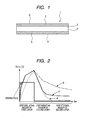
- Fig. 1 is a cross-sectional view of the main structure of a thermal head according to an embodiment of the invention.
- a thermal head 1 has three-layer structure that includes a heat insulating layer 2 on which heating elements are formed, a heat radiating layer 3 that is provided under the heat insulating layer 2, and a heat storing layer 4 that is provided under the heat radiating layer 3.
- Each of the heat insulating layer 2 and the heat storing layer 4 is a glass layer 5 that is made of the same glaze material formed by known high-temperature firing, and the heat radiating layer 3 is formed of a ceramic layer 6.
- Heating elements, electrode patterns, a passivation film, and the like are formed on the upper surface of the glass layer that functions as the heat insulating layer 2.
- the heat radiating layer 3 which is provided under the heat insulating layer 2, appropriately radiates heat, which is generated by the heating elements formed on the heat insulating layer 2, through heat sinks (not shown) and the like. Further, the heat storing layer 4, which is provided under the heat radiating layer 3, stores heat that is generated by the heating elements.
- glass having low thermal diffusivity (0.2 to 0.4 mm 2 /sec) is used for the glass layer 5 that forms each of the heat insulating layer 2 and the heat storing layer 4.
- the thickness of the glass layer 5 is small as described above, the glass layer 5 is apt to be broken in a manufacturing process, so that it is difficult to handle the glass layer 5.
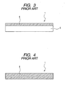
- the thickness of the glass layer 5 is large, heat is excessively stored in the glass layer 5, so that dots of printing results are deformed or a phenomenon such as so-called tailing is apt to occur. Accordingly, it is important to adjust the thickness of the glass layer 5 so that the heat storing layer 4 can store heat at appropriate temperature as shown in Fig. 2 , for example, until the next pulse current is supplied to the thermal head after the insulation and radiation when one pulse current is supplied to the thermal head (one dot).
- Fig. 2 shows the temperature change (graph denoted by "A” in Fig. 2 ) of a thermal head (see Fig. 3 ) in the related art having two-layer structure where a glaze glass layer functioning as a heat storing layer 4 is formed on the upper surface of a ceramic substrate, the temperature change (graph denoted by "B” in Fig. 2 ) of a thermal head (see Fig. 4 ) having single-layer structure where a glass layer having low thermal diffusivity is thick, and the temperature change (graph denoted by "C” in Fig. 2 ) of the thermal head 1 having three-layer structure according to this embodiment.
- thermal diffusivity of the glaze glass layer of the thermal head corresponding to the graph denoted by "A" in Fig. 2 is high as shown in Fig. 2 , much time (start-up time) is required until the temperature of a heating element reaches temperature suitable for printing as compared to the other two thermal heads. That is, immediately after current is supplied (one pulse current is applied), thermal responsiveness deteriorates (see a heat insulating region). Further, since the heat radiating layer 3 (ceramic layer 6) radiates heat, it is possible to prevent heat from being excessively stored. However, in contrast, it is understood that there also is no heat storage effect (see a heat storing region). Meanwhile, the thermal head, which corresponds to the graph denoted by "B" in Fig.
- the thermal head 2 is formed of a single glass layer 5 having low thermal diffusivity. Accordingly, if one pulse current is applied to this thermal head, the temperature of the heating element instantly rises. However, a heat radiation effect is small, so that heat is excessively stored (see a heat storing region). Therefore, if the next current is supplied (one pulse current is applied), the heating element is overheated more than necessary. For this reason, there is a concern that printed dots are deformed or so-called tailing occurs. Accordingly, the thickness of the glass layer 5 is adjusted so that the thermal head shows the balance of the thermal responsiveness corresponding to the graph denoted by "C" in Fig. 2 .
- the heat storing layer is spaced apart from the heating elements formed on the heat insulating layer. Accordingly, it may be possible to lower the driving voltage applied to the heating element without defective printing that is caused by excessive heat storage in the vicinity of the heating element. As a result, it may be possible to achieve power saving.
- the thicknesses of the heat insulating layer 2 and the heat storing layer 4, which are formed on and under the heat radiating layer 3, are not limited to the same thickness, and may be controlled according to the energy that causes heat generation. Accordingly, it is possible to increase the degree of freedom in designing a thermal head.
- the material of the heat radiating layer 3 is not limited to a ceramic material.
- a metalloid material such as silicon or a metal material such as aluminum may be used as the material of the heat radiating layer 3.
- the thermal head 1 is not formed of only glass layers 5 and the heat radiating layer 3 formed of a ceramic layer 6 is interposed between the glass layers 5, it is easy to handle the thermal head 1 in the manufacturing process.
Landscapes
- Electronic Switches (AREA)
- Resistance Heating (AREA)
- Surface Heating Bodies (AREA)
Abstract
Description
- The present invention contains subject matter related to Japanese Patent Application No.
2008-150375 - The present invention relates to a thermal head that uses a glass layer having low thermal diffusivity.
- In the past, there has been used a thermal head having two-layer structure where a glass layer functioning as a heat storing layer is formed on the upper surface of a ceramic substrate made of alumina ceramic or the like as shown in
Fig. 3 , or athermal head 1 that is formed of a single glass layer as shown inFig. 4 (for example, see Japanese Unexamined Patent Application Publication No.2004-50712 02-200452 - The glass layer of the thermal head having the two-layer structure is formed by printing a pasty glaze material on the upper surface of the ceramic substrate, and performing high-temperature firing. However, since the coefficient of thermal expansion of a material of the ceramic substrate is different from that of the glaze material of the glass layer, there has been a problem in that warpage occurs on the glass substrate after the high-temperature firing or cracks are generated on a laminate interface. Accordingly, specifications, such as the thickness of the glass layer or the ceramic substrate, the aspect ratio of the substrate, and an area ratio, was adjusted in order to cope with the problem such as warpage or the like. However, it was very difficult to adjust the specifications.
- Further, the thickness of the thermal head formed of a single glass layer is set to 0.5 mm or less in order to obtain excellent printing characteristics. However, since the thin thermal head is apt to be broken when being handled in the manufacturing process, there has been a problem in that it is difficult to handle the thermal head. In order to solve this problem, it has been considered that the thickness of the glass layer is increased. However, since heat is excessively stored in the thermal head, there has been generated another problem in that printing characteristics deteriorate due to an ink mark such as so-called tailing.
- An advantage of some aspects of the invention is to provide a thermal head that can easily solve problems such as handling and warpage of a substrate during manufacture, has large the degree of freedom in designing a substrate, and can effectively achieve power saving.
- According to an aspect of the invention, a thermal head has three-layer structure that includes a heat insulating layer on which heating elements are formed, a heat radiating layer that is provided under the heat insulating layer, and a heat storing layer that is provided under the heat radiating layer.
- In the thermal head, the heating elements formed on the heat insulating layer are disposed so as to be spaced apart from the heat storing layer provided under the heat radiating layer. Accordingly, if thermal responsiveness, a heat radiating property, and a heat storing property according to the thermal diffusivity of each layer are considered, it is possible to easily and appropriately design a thermal head so as to save power.
- Further, in the thermal head according to the aspect of the invention, each of the heat insulating layer and the heat storing layer may be a glass layer that is made of the same material formed by high-temperature firing.
- In the thermal head, glass layers made of the same material are formed on and under the heat radiating layer, so that the deformation caused by thermal stress, that is, the warpage of the substrate may be effectively suppressed. A material, which allows heat to be easily controlled, may be selected for the heat radiating layer that is disposed between the heat insulating layer and the heat storing layer. In addition, the total thickness of the thermal head is also increased due to the three-layer structure, and the thermal head is also easily handled in a manufacturing process.
- As described above, the thermal head according to the aspect of the invention has advantages of easily solving problems such as handling and warpage of a substrate during manufacture, having large the degree of freedom in designing a substrate, and effectively achieving power saving.
-
-
Fig. 1 is a cross-sectional view of the main structure of a thermal head according to an embodiment of the invention. -
Fig. 2 is an image view describing the thermal responsiveness of the thermal head according to the embodiment of the invention while the thermal head is compared with a thermal head in the related art. -
Fig. 3 is a cross-sectional view of the main structure of a thermal head in the related art. -
Fig. 4 is a cross-sectional view of the main structure of another thermal head in the related art. -
Fig. 1 is a cross-sectional view of the main structure of a thermal head according to an embodiment of the invention. - A
thermal head 1 according to the embodiment has three-layer structure that includes aheat insulating layer 2 on which heating elements are formed, a heat radiatinglayer 3 that is provided under theheat insulating layer 2, and aheat storing layer 4 that is provided under theheat radiating layer 3. - Each of the
heat insulating layer 2 and theheat storing layer 4 is aglass layer 5 that is made of the same glaze material formed by known high-temperature firing, and theheat radiating layer 3 is formed of aceramic layer 6. - Heating elements, electrode patterns, a passivation film, and the like are formed on the upper surface of the glass layer that functions as the
heat insulating layer 2. - Further, the
heat radiating layer 3, which is provided under theheat insulating layer 2, appropriately radiates heat, which is generated by the heating elements formed on theheat insulating layer 2, through heat sinks (not shown) and the like. Further, theheat storing layer 4, which is provided under theheat radiating layer 3, stores heat that is generated by the heating elements. - In this embodiment, glass having low thermal diffusivity (0.2 to 0.4 mm2/sec) is used for the
glass layer 5 that forms each of theheat insulating layer 2 and theheat storing layer 4. If the thickness of theglass layer 5 is small as described above, theglass layer 5 is apt to be broken in a manufacturing process, so that it is difficult to handle theglass layer 5. If the thickness of theglass layer 5 is large, heat is excessively stored in theglass layer 5, so that dots of printing results are deformed or a phenomenon such as so-called tailing is apt to occur. Accordingly, it is important to adjust the thickness of theglass layer 5 so that theheat storing layer 4 can store heat at appropriate temperature as shown inFig. 2 , for example, until the next pulse current is supplied to the thermal head after the insulation and radiation when one pulse current is supplied to the thermal head (one dot). - Meanwhile,
Fig. 2 shows the temperature change (graph denoted by "A" inFig. 2 ) of a thermal head (seeFig. 3 ) in the related art having two-layer structure where a glaze glass layer functioning as aheat storing layer 4 is formed on the upper surface of a ceramic substrate, the temperature change (graph denoted by "B" inFig. 2 ) of a thermal head (seeFig. 4 ) having single-layer structure where a glass layer having low thermal diffusivity is thick, and the temperature change (graph denoted by "C" inFig. 2 ) of thethermal head 1 having three-layer structure according to this embodiment. - Since the thermal diffusivity of the glaze glass layer of the thermal head corresponding to the graph denoted by "A" in
Fig. 2 is high as shown inFig. 2 , much time (start-up time) is required until the temperature of a heating element reaches temperature suitable for printing as compared to the other two thermal heads. That is, immediately after current is supplied (one pulse current is applied), thermal responsiveness deteriorates (see a heat insulating region). Further, since the heat radiating layer 3 (ceramic layer 6) radiates heat, it is possible to prevent heat from being excessively stored. However, in contrast, it is understood that there also is no heat storage effect (see a heat storing region). Meanwhile, the thermal head, which corresponds to the graph denoted by "B" inFig. 2 , is formed of asingle glass layer 5 having low thermal diffusivity. Accordingly, if one pulse current is applied to this thermal head, the temperature of the heating element instantly rises. However, a heat radiation effect is small, so that heat is excessively stored (see a heat storing region). Therefore, if the next current is supplied (one pulse current is applied), the heating element is overheated more than necessary. For this reason, there is a concern that printed dots are deformed or so-called tailing occurs. Accordingly, the thickness of theglass layer 5 is adjusted so that the thermal head shows the balance of the thermal responsiveness corresponding to the graph denoted by "C" inFig. 2 . In contrast, since the temperature of the heating element of the thermal head corresponding to the graph denoted by "C" inFig. 2 can instantly rise (see a heat insulating region) by the application of one pulse current, an appropriate heat storage effect is obtained without excessive heat radiation (see a heat radiating region and a heat storing region). Accordingly, it is possible to reduce energy by lowering a driving voltage to be applied next time. - As described above, in the thermal head according to this embodiment, the heat storing layer is spaced apart from the heating elements formed on the heat insulating layer. Accordingly, it may be possible to lower the driving voltage applied to the heating element without defective printing that is caused by excessive heat storage in the vicinity of the heating element. As a result, it may be possible to achieve power saving.
- Further, glass layers made of the same material are formed on and under the
heat radiating layer 3, so that the deformation caused by thermal stress, that is, the warpage of the substrate may be effectively suppressed. Meanwhile, the thicknesses of theheat insulating layer 2 and the heat storinglayer 4, which are formed on and under theheat radiating layer 3, are not limited to the same thickness, and may be controlled according to the energy that causes heat generation. Accordingly, it is possible to increase the degree of freedom in designing a thermal head. - Furthermore, a material, which allows heat to be easily controlled, may be selected for the
heat radiating layer 3 that is disposed between theheat insulating layer 2 and theheat storing layer 4. That is, the material of theheat radiating layer 3 is not limited to a ceramic material. For example, a metalloid material such as silicon or a metal material such as aluminum may be used as the material of theheat radiating layer 3. - Meanwhile, since the
thermal head 1 is not formed ofonly glass layers 5 and theheat radiating layer 3 formed of aceramic layer 6 is interposed between theglass layers 5, it is easy to handle thethermal head 1 in the manufacturing process. - It should be understood by those skilled in the art that various modifications, combinations, sub-combinations and alterations may occur depending on design requirements and other factors insofar as they are within the scope of the appended claims of the equivalents thereof.
Claims (3)
- A thermal head having three-layer structure that includes a heat insulating layer on which heating elements are formed, a heat radiating layer that is provided under the heat insulating layer, and a heat storing layer that is provided under the heat radiating layer.
- The thermal head according to claim 1,
wherein each of the heat insulating layer and the heat storing layer is a glass layer that is made of the same material formed by high-temperature firing. - The thermal head according to claim 1 or 2,
wherein the glass layer has thermal diffusivity in the range of 0.2 to 0.4 (mm2/sec).
Applications Claiming Priority (1)
| Application Number | Priority Date | Filing Date | Title |
|---|---|---|---|
| JP2008150375A JP2009292119A (en) | 2008-06-09 | 2008-06-09 | Thermal head |
Publications (3)
| Publication Number | Publication Date |
|---|---|
| EP2133207A2 true EP2133207A2 (en) | 2009-12-16 |
| EP2133207A3 EP2133207A3 (en) | 2010-07-21 |
| EP2133207B1 EP2133207B1 (en) | 2011-10-12 |
Family
ID=41066644
Family Applications (1)
| Application Number | Title | Priority Date | Filing Date |
|---|---|---|---|
| EP09006973A Not-in-force EP2133207B1 (en) | 2008-06-09 | 2009-05-25 | Thermal head |
Country Status (5)
| Country | Link |
|---|---|
| US (1) | US20090305056A1 (en) |
| EP (1) | EP2133207B1 (en) |
| JP (1) | JP2009292119A (en) |
| CN (1) | CN101602293A (en) |
| AT (1) | ATE528143T1 (en) |
Families Citing this family (2)
| Publication number | Priority date | Publication date | Assignee | Title |
|---|---|---|---|---|
| CN109968826B (en) * | 2017-03-20 | 2020-04-10 | 深圳市博思得科技发展有限公司 | Thermal print head |
| JP7606861B2 (en) | 2020-12-04 | 2024-12-26 | ローム株式会社 | Thermal printhead, its manufacturing method, and thermal printer |
Citations (3)
| Publication number | Priority date | Publication date | Assignee | Title |
|---|---|---|---|---|
| JPH02200452A (en) | 1989-01-31 | 1990-08-08 | Shinko Electric Co Ltd | Metallic substrate for thermal head |
| JP2004050712A (en) | 2002-07-23 | 2004-02-19 | Aoi Electronics Co Ltd | Glaze substrate and thermal head |
| JP2008150375A (en) | 2006-12-14 | 2008-07-03 | Novartis Ag | Production method |
Family Cites Families (11)
| Publication number | Priority date | Publication date | Assignee | Title |
|---|---|---|---|---|
| DE3536268A1 (en) * | 1985-10-11 | 1987-04-16 | Bayer Ag | SURFACE HEATING ELEMENTS |
| JPS62278058A (en) * | 1986-05-27 | 1987-12-02 | Matsushita Electric Ind Co Ltd | Thermal head |
| JPS6391262A (en) * | 1986-10-06 | 1988-04-21 | Hitachi Ltd | Constitution of thermal head |
| JPS63118271A (en) * | 1986-11-07 | 1988-05-23 | Tdk Corp | Substrate for thermal head and manufacture thereof |
| JPS6463162A (en) * | 1987-09-03 | 1989-03-09 | Hitachi Ltd | Thermal recording head |
| JP2550400B2 (en) * | 1988-10-31 | 1996-11-06 | 松下電器産業株式会社 | Insulating substrate and thermal head using the same |
| US5252988A (en) * | 1989-12-15 | 1993-10-12 | Sharp Kabushiki Kaisha | Thermal head for thermal recording machine |
| JP3133081B2 (en) * | 1991-01-22 | 2001-02-05 | 株式会社東芝 | Thermal head |
| JP3305764B2 (en) * | 1992-07-28 | 2002-07-24 | ニッコー株式会社 | Method for manufacturing substrate for thermal head |
| JP2002307732A (en) * | 2001-04-16 | 2002-10-23 | Alps Electric Co Ltd | Thermal head |
| JP2006272891A (en) * | 2005-03-30 | 2006-10-12 | Fuji Photo Film Co Ltd | Thermal-storage correcting method, thermal printer and thermal-storage correcting program |
-
2008
- 2008-06-09 JP JP2008150375A patent/JP2009292119A/en not_active Withdrawn
-
2009
- 2009-05-21 CN CNA2009101389618A patent/CN101602293A/en active Pending
- 2009-05-25 AT AT09006973T patent/ATE528143T1/en not_active IP Right Cessation
- 2009-05-25 EP EP09006973A patent/EP2133207B1/en not_active Not-in-force
- 2009-06-03 US US12/477,415 patent/US20090305056A1/en not_active Abandoned
Patent Citations (3)
| Publication number | Priority date | Publication date | Assignee | Title |
|---|---|---|---|---|
| JPH02200452A (en) | 1989-01-31 | 1990-08-08 | Shinko Electric Co Ltd | Metallic substrate for thermal head |
| JP2004050712A (en) | 2002-07-23 | 2004-02-19 | Aoi Electronics Co Ltd | Glaze substrate and thermal head |
| JP2008150375A (en) | 2006-12-14 | 2008-07-03 | Novartis Ag | Production method |
Also Published As
| Publication number | Publication date |
|---|---|
| ATE528143T1 (en) | 2011-10-15 |
| EP2133207B1 (en) | 2011-10-12 |
| EP2133207A3 (en) | 2010-07-21 |
| JP2009292119A (en) | 2009-12-17 |
| US20090305056A1 (en) | 2009-12-10 |
| CN101602293A (en) | 2009-12-16 |
Similar Documents
| Publication | Publication Date | Title |
|---|---|---|
| US9414512B2 (en) | Substrate for power module, substrate with heat sink for power module, power module, method for producing substrate for power module, and method for producing substrate with heat sink for power module | |
| WO2015111520A1 (en) | Thermal print head and thermal printer | |
| EP2364855B1 (en) | Thermal head, printer, and manufacturing method for the thermal head | |
| RU2414354C1 (en) | Base of head for liquid discharge, method of its manufacturing and liquid discharge head | |
| CN100572081C (en) | thermal print head | |
| US10121574B2 (en) | Resistor and method for manufacturing resistor | |
| JP6676369B2 (en) | Thermal printhead and thermal printer | |
| EP2133207B1 (en) | Thermal head | |
| US7969458B2 (en) | Thermal printhead | |
| US9302495B2 (en) | Thermal head, printer, and method of manufacturing thermal head | |
| JP3868755B2 (en) | Thermal head and manufacturing method thereof | |
| JP2005280203A (en) | Thermal head and its manufacturing method | |
| US11355408B2 (en) | Method of manufacturing insulating circuit board with heatsink | |
| JP6584641B2 (en) | Thermal head and thermal printer | |
| JP2010238965A (en) | Power module substrate, power module substrate manufacturing method, and power module | |
| JP2019098667A (en) | Thermal print head | |
| CN216545361U (en) | Heating substrate for thermal printing head | |
| JP2012056279A (en) | Thermal head | |
| JP2018062152A (en) | Thermal print head | |
| CN221067546U (en) | Spliced thermal print head | |
| JP2007185830A (en) | Thermal head and method for manufacturing the same | |
| JP2001260403A (en) | Thermal and manufacturing method | |
| CN215970712U (en) | Thermal print head | |
| JP2010061834A (en) | Method for manufacturing heater | |
| JP2005329561A (en) | Thermal head and printer |
Legal Events
| Date | Code | Title | Description |
|---|---|---|---|
| PUAI | Public reference made under article 153(3) epc to a published international application that has entered the european phase |
Free format text: ORIGINAL CODE: 0009012 |
|
| AK | Designated contracting states |
Kind code of ref document: A2 Designated state(s): AT BE BG CH CY CZ DE DK EE ES FI FR GB GR HR HU IE IS IT LI LT LU LV MC MK MT NL NO PL PT RO SE SI SK TR |
|
| PUAL | Search report despatched |
Free format text: ORIGINAL CODE: 0009013 |
|
| AK | Designated contracting states |
Kind code of ref document: A3 Designated state(s): AT BE BG CH CY CZ DE DK EE ES FI FR GB GR HR HU IE IS IT LI LT LU LV MC MK MT NL NO PL PT RO SE SI SK TR |
|
| AX | Request for extension of the european patent |
Extension state: AL BA RS |
|
| 17P | Request for examination filed |
Effective date: 20110112 |
|
| GRAP | Despatch of communication of intention to grant a patent |
Free format text: ORIGINAL CODE: EPIDOSNIGR1 |
|
| RIC1 | Information provided on ipc code assigned before grant |
Ipc: B41J 2/335 20060101AFI20110318BHEP |
|
| GRAS | Grant fee paid |
Free format text: ORIGINAL CODE: EPIDOSNIGR3 |
|
| GRAA | (expected) grant |
Free format text: ORIGINAL CODE: 0009210 |
|
| AK | Designated contracting states |
Kind code of ref document: B1 Designated state(s): AT BE BG CH CY CZ DE DK EE ES FI FR GB GR HR HU IE IS IT LI LT LU LV MC MK MT NL NO PL PT RO SE SI SK TR |
|
| REG | Reference to a national code |
Ref country code: GB Ref legal event code: FG4D |
|
| REG | Reference to a national code |
Ref country code: CH Ref legal event code: EP |
|
| REG | Reference to a national code |
Ref country code: IE Ref legal event code: FG4D |
|
| REG | Reference to a national code |
Ref country code: DE Ref legal event code: R096 Ref document number: 602009002979 Country of ref document: DE Effective date: 20111215 |
|
| REG | Reference to a national code |
Ref country code: NL Ref legal event code: VDEP Effective date: 20111012 |
|
| LTIE | Lt: invalidation of european patent or patent extension |
Effective date: 20111012 |
|
| REG | Reference to a national code |
Ref country code: AT Ref legal event code: MK05 Ref document number: 528143 Country of ref document: AT Kind code of ref document: T Effective date: 20111012 |
|
| PG25 | Lapsed in a contracting state [announced via postgrant information from national office to epo] |
Ref country code: IS Free format text: LAPSE BECAUSE OF FAILURE TO SUBMIT A TRANSLATION OF THE DESCRIPTION OR TO PAY THE FEE WITHIN THE PRESCRIBED TIME-LIMIT Effective date: 20120212 Ref country code: NO Free format text: LAPSE BECAUSE OF FAILURE TO SUBMIT A TRANSLATION OF THE DESCRIPTION OR TO PAY THE FEE WITHIN THE PRESCRIBED TIME-LIMIT Effective date: 20120112 Ref country code: BE Free format text: LAPSE BECAUSE OF FAILURE TO SUBMIT A TRANSLATION OF THE DESCRIPTION OR TO PAY THE FEE WITHIN THE PRESCRIBED TIME-LIMIT Effective date: 20111012 Ref country code: LT Free format text: LAPSE BECAUSE OF FAILURE TO SUBMIT A TRANSLATION OF THE DESCRIPTION OR TO PAY THE FEE WITHIN THE PRESCRIBED TIME-LIMIT Effective date: 20111012 |
|
| PG25 | Lapsed in a contracting state [announced via postgrant information from national office to epo] |
Ref country code: SE Free format text: LAPSE BECAUSE OF FAILURE TO SUBMIT A TRANSLATION OF THE DESCRIPTION OR TO PAY THE FEE WITHIN THE PRESCRIBED TIME-LIMIT Effective date: 20111012 Ref country code: PT Free format text: LAPSE BECAUSE OF FAILURE TO SUBMIT A TRANSLATION OF THE DESCRIPTION OR TO PAY THE FEE WITHIN THE PRESCRIBED TIME-LIMIT Effective date: 20120213 Ref country code: GR Free format text: LAPSE BECAUSE OF FAILURE TO SUBMIT A TRANSLATION OF THE DESCRIPTION OR TO PAY THE FEE WITHIN THE PRESCRIBED TIME-LIMIT Effective date: 20120113 Ref country code: HR Free format text: LAPSE BECAUSE OF FAILURE TO SUBMIT A TRANSLATION OF THE DESCRIPTION OR TO PAY THE FEE WITHIN THE PRESCRIBED TIME-LIMIT Effective date: 20111012 Ref country code: NL Free format text: LAPSE BECAUSE OF FAILURE TO SUBMIT A TRANSLATION OF THE DESCRIPTION OR TO PAY THE FEE WITHIN THE PRESCRIBED TIME-LIMIT Effective date: 20111012 Ref country code: LV Free format text: LAPSE BECAUSE OF FAILURE TO SUBMIT A TRANSLATION OF THE DESCRIPTION OR TO PAY THE FEE WITHIN THE PRESCRIBED TIME-LIMIT Effective date: 20111012 Ref country code: SI Free format text: LAPSE BECAUSE OF FAILURE TO SUBMIT A TRANSLATION OF THE DESCRIPTION OR TO PAY THE FEE WITHIN THE PRESCRIBED TIME-LIMIT Effective date: 20111012 |
|
| PG25 | Lapsed in a contracting state [announced via postgrant information from national office to epo] |
Ref country code: CY Free format text: LAPSE BECAUSE OF FAILURE TO SUBMIT A TRANSLATION OF THE DESCRIPTION OR TO PAY THE FEE WITHIN THE PRESCRIBED TIME-LIMIT Effective date: 20111012 |
|
| PG25 | Lapsed in a contracting state [announced via postgrant information from national office to epo] |
Ref country code: SK Free format text: LAPSE BECAUSE OF FAILURE TO SUBMIT A TRANSLATION OF THE DESCRIPTION OR TO PAY THE FEE WITHIN THE PRESCRIBED TIME-LIMIT Effective date: 20111012 Ref country code: CZ Free format text: LAPSE BECAUSE OF FAILURE TO SUBMIT A TRANSLATION OF THE DESCRIPTION OR TO PAY THE FEE WITHIN THE PRESCRIBED TIME-LIMIT Effective date: 20111012 Ref country code: DK Free format text: LAPSE BECAUSE OF FAILURE TO SUBMIT A TRANSLATION OF THE DESCRIPTION OR TO PAY THE FEE WITHIN THE PRESCRIBED TIME-LIMIT Effective date: 20111012 Ref country code: BG Free format text: LAPSE BECAUSE OF FAILURE TO SUBMIT A TRANSLATION OF THE DESCRIPTION OR TO PAY THE FEE WITHIN THE PRESCRIBED TIME-LIMIT Effective date: 20120112 Ref country code: EE Free format text: LAPSE BECAUSE OF FAILURE TO SUBMIT A TRANSLATION OF THE DESCRIPTION OR TO PAY THE FEE WITHIN THE PRESCRIBED TIME-LIMIT Effective date: 20111012 |
|
| PGFP | Annual fee paid to national office [announced via postgrant information from national office to epo] |
Ref country code: DE Payment date: 20120531 Year of fee payment: 4 |
|
| PLBE | No opposition filed within time limit |
Free format text: ORIGINAL CODE: 0009261 |
|
| STAA | Information on the status of an ep patent application or granted ep patent |
Free format text: STATUS: NO OPPOSITION FILED WITHIN TIME LIMIT |
|
| PG25 | Lapsed in a contracting state [announced via postgrant information from national office to epo] |
Ref country code: PL Free format text: LAPSE BECAUSE OF FAILURE TO SUBMIT A TRANSLATION OF THE DESCRIPTION OR TO PAY THE FEE WITHIN THE PRESCRIBED TIME-LIMIT Effective date: 20111012 Ref country code: RO Free format text: LAPSE BECAUSE OF FAILURE TO SUBMIT A TRANSLATION OF THE DESCRIPTION OR TO PAY THE FEE WITHIN THE PRESCRIBED TIME-LIMIT Effective date: 20111012 Ref country code: IT Free format text: LAPSE BECAUSE OF FAILURE TO SUBMIT A TRANSLATION OF THE DESCRIPTION OR TO PAY THE FEE WITHIN THE PRESCRIBED TIME-LIMIT Effective date: 20111012 |
|
| 26N | No opposition filed |
Effective date: 20120713 |
|
| REG | Reference to a national code |
Ref country code: DE Ref legal event code: R097 Ref document number: 602009002979 Country of ref document: DE Effective date: 20120713 |
|
| PG25 | Lapsed in a contracting state [announced via postgrant information from national office to epo] |
Ref country code: MC Free format text: LAPSE BECAUSE OF NON-PAYMENT OF DUE FEES Effective date: 20120531 |
|
| PG25 | Lapsed in a contracting state [announced via postgrant information from national office to epo] |
Ref country code: AT Free format text: LAPSE BECAUSE OF FAILURE TO SUBMIT A TRANSLATION OF THE DESCRIPTION OR TO PAY THE FEE WITHIN THE PRESCRIBED TIME-LIMIT Effective date: 20111012 |
|
| REG | Reference to a national code |
Ref country code: IE Ref legal event code: MM4A |
|
| PG25 | Lapsed in a contracting state [announced via postgrant information from national office to epo] |
Ref country code: MK Free format text: LAPSE BECAUSE OF FAILURE TO SUBMIT A TRANSLATION OF THE DESCRIPTION OR TO PAY THE FEE WITHIN THE PRESCRIBED TIME-LIMIT Effective date: 20111012 |
|
| REG | Reference to a national code |
Ref country code: FR Ref legal event code: ST Effective date: 20130131 |
|
| PG25 | Lapsed in a contracting state [announced via postgrant information from national office to epo] |
Ref country code: IE Free format text: LAPSE BECAUSE OF NON-PAYMENT OF DUE FEES Effective date: 20120525 Ref country code: ES Free format text: LAPSE BECAUSE OF FAILURE TO SUBMIT A TRANSLATION OF THE DESCRIPTION OR TO PAY THE FEE WITHIN THE PRESCRIBED TIME-LIMIT Effective date: 20120123 Ref country code: FR Free format text: LAPSE BECAUSE OF NON-PAYMENT OF DUE FEES Effective date: 20120531 |
|
| PG25 | Lapsed in a contracting state [announced via postgrant information from national office to epo] |
Ref country code: FI Free format text: LAPSE BECAUSE OF FAILURE TO SUBMIT A TRANSLATION OF THE DESCRIPTION OR TO PAY THE FEE WITHIN THE PRESCRIBED TIME-LIMIT Effective date: 20111012 |
|
| PG25 | Lapsed in a contracting state [announced via postgrant information from national office to epo] |
Ref country code: MT Free format text: LAPSE BECAUSE OF FAILURE TO SUBMIT A TRANSLATION OF THE DESCRIPTION OR TO PAY THE FEE WITHIN THE PRESCRIBED TIME-LIMIT Effective date: 20111012 |
|
| REG | Reference to a national code |
Ref country code: CH Ref legal event code: PL |
|
| GBPC | Gb: european patent ceased through non-payment of renewal fee |
Effective date: 20130525 |
|
| PG25 | Lapsed in a contracting state [announced via postgrant information from national office to epo] |
Ref country code: DE Free format text: LAPSE BECAUSE OF NON-PAYMENT OF DUE FEES Effective date: 20131203 Ref country code: CH Free format text: LAPSE BECAUSE OF NON-PAYMENT OF DUE FEES Effective date: 20130531 Ref country code: LI Free format text: LAPSE BECAUSE OF NON-PAYMENT OF DUE FEES Effective date: 20130531 |
|
| REG | Reference to a national code |
Ref country code: DE Ref legal event code: R119 Ref document number: 602009002979 Country of ref document: DE Effective date: 20131203 |
|
| PG25 | Lapsed in a contracting state [announced via postgrant information from national office to epo] |
Ref country code: GB Free format text: LAPSE BECAUSE OF NON-PAYMENT OF DUE FEES Effective date: 20130525 Ref country code: TR Free format text: LAPSE BECAUSE OF FAILURE TO SUBMIT A TRANSLATION OF THE DESCRIPTION OR TO PAY THE FEE WITHIN THE PRESCRIBED TIME-LIMIT Effective date: 20111012 |
|
| PG25 | Lapsed in a contracting state [announced via postgrant information from national office to epo] |
Ref country code: LU Free format text: LAPSE BECAUSE OF NON-PAYMENT OF DUE FEES Effective date: 20120525 |
|
| PG25 | Lapsed in a contracting state [announced via postgrant information from national office to epo] |
Ref country code: HU Free format text: LAPSE BECAUSE OF FAILURE TO SUBMIT A TRANSLATION OF THE DESCRIPTION OR TO PAY THE FEE WITHIN THE PRESCRIBED TIME-LIMIT Effective date: 20090525 |