EP2131374A1 - Ceramic electronic component with diffusion bonding between external electrode and metal terminal, and method for manufacturing the same - Google Patents
Ceramic electronic component with diffusion bonding between external electrode and metal terminal, and method for manufacturing the same Download PDFInfo
- Publication number
- EP2131374A1 EP2131374A1 EP09004990A EP09004990A EP2131374A1 EP 2131374 A1 EP2131374 A1 EP 2131374A1 EP 09004990 A EP09004990 A EP 09004990A EP 09004990 A EP09004990 A EP 09004990A EP 2131374 A1 EP2131374 A1 EP 2131374A1
- Authority
- EP
- European Patent Office
- Prior art keywords
- external electrode
- metal
- electronic component
- metal terminal
- terminal
- Prior art date
- Legal status (The legal status is an assumption and is not a legal conclusion. Google has not performed a legal analysis and makes no representation as to the accuracy of the status listed.)
- Granted
Links
- 229910052751 metal Inorganic materials 0.000 title claims abstract description 209
- 239000002184 metal Substances 0.000 title claims abstract description 209
- 239000000919 ceramic Substances 0.000 title claims abstract description 147
- 238000000034 method Methods 0.000 title claims abstract description 38
- 238000004519 manufacturing process Methods 0.000 title claims abstract description 21
- 238000009792 diffusion process Methods 0.000 title claims abstract description 10
- 238000007747 plating Methods 0.000 claims description 46
- 238000010438 heat treatment Methods 0.000 claims description 26
- 229910045601 alloy Inorganic materials 0.000 claims description 17
- 239000000956 alloy Substances 0.000 claims description 17
- 150000002739 metals Chemical class 0.000 claims description 16
- 229910052709 silver Inorganic materials 0.000 claims description 11
- 229910052802 copper Inorganic materials 0.000 claims description 10
- 229910052759 nickel Inorganic materials 0.000 claims description 10
- 238000005260 corrosion Methods 0.000 claims description 5
- 229910052742 iron Inorganic materials 0.000 claims description 5
- 229910052804 chromium Inorganic materials 0.000 claims description 4
- 229910052737 gold Inorganic materials 0.000 claims description 3
- 229910052763 palladium Inorganic materials 0.000 claims description 3
- 229910052718 tin Inorganic materials 0.000 claims description 3
- 239000002923 metal particle Substances 0.000 abstract description 4
- 230000007423 decrease Effects 0.000 description 16
- 230000015572 biosynthetic process Effects 0.000 description 13
- 229910000679 solder Inorganic materials 0.000 description 12
- 238000012360 testing method Methods 0.000 description 12
- 238000011161 development Methods 0.000 description 10
- 239000010949 copper Substances 0.000 description 9
- 230000008569 process Effects 0.000 description 9
- 238000003466 welding Methods 0.000 description 9
- 239000011521 glass Substances 0.000 description 8
- 239000000463 material Substances 0.000 description 8
- 238000010304 firing Methods 0.000 description 7
- 230000035939 shock Effects 0.000 description 7
- 239000000758 substrate Substances 0.000 description 5
- 230000006866 deterioration Effects 0.000 description 4
- 239000000203 mixture Substances 0.000 description 4
- 239000000843 powder Substances 0.000 description 4
- 238000001816 cooling Methods 0.000 description 3
- 230000003247 decreasing effect Effects 0.000 description 3
- 238000007667 floating Methods 0.000 description 3
- RAXXELZNTBOGNW-UHFFFAOYSA-N imidazole Natural products C1=CNC=N1 RAXXELZNTBOGNW-UHFFFAOYSA-N 0.000 description 3
- RYGMFSIKBFXOCR-UHFFFAOYSA-N Copper Chemical compound [Cu] RYGMFSIKBFXOCR-UHFFFAOYSA-N 0.000 description 2
- 229910001252 Pd alloy Inorganic materials 0.000 description 2
- 239000012298 atmosphere Substances 0.000 description 2
- 239000011230 binding agent Substances 0.000 description 2
- 239000003985 ceramic capacitor Substances 0.000 description 2
- 229910000765 intermetallic Inorganic materials 0.000 description 2
- 239000003960 organic solvent Substances 0.000 description 2
- 239000002245 particle Substances 0.000 description 2
- 230000009467 reduction Effects 0.000 description 2
- 239000000523 sample Substances 0.000 description 2
- WFKWXMTUELFFGS-UHFFFAOYSA-N tungsten Chemical compound [W] WFKWXMTUELFFGS-UHFFFAOYSA-N 0.000 description 2
- 229910052721 tungsten Inorganic materials 0.000 description 2
- 239000010937 tungsten Substances 0.000 description 2
- 229910020935 Sn-Sb Inorganic materials 0.000 description 1
- 229910008757 Sn—Sb Inorganic materials 0.000 description 1
- 238000000429 assembly Methods 0.000 description 1
- 230000000712 assembly Effects 0.000 description 1
- 229910002113 barium titanate Inorganic materials 0.000 description 1
- QRUDEWIWKLJBPS-UHFFFAOYSA-N benzotriazole Chemical compound C1=CC=C2N[N][N]C2=C1 QRUDEWIWKLJBPS-UHFFFAOYSA-N 0.000 description 1
- 239000012964 benzotriazole Substances 0.000 description 1
- 239000003990 capacitor Substances 0.000 description 1
- 230000008859 change Effects 0.000 description 1
- 239000011248 coating agent Substances 0.000 description 1
- 238000000576 coating method Methods 0.000 description 1
- 230000000052 comparative effect Effects 0.000 description 1
- 239000000470 constituent Substances 0.000 description 1
- 238000002474 experimental method Methods 0.000 description 1
- 239000000383 hazardous chemical Substances 0.000 description 1
- 230000020169 heat generation Effects 0.000 description 1
- 238000007373 indentation Methods 0.000 description 1
- 239000004615 ingredient Substances 0.000 description 1
- 238000000462 isostatic pressing Methods 0.000 description 1
- 238000003475 lamination Methods 0.000 description 1
- 238000002844 melting Methods 0.000 description 1
- 230000008018 melting Effects 0.000 description 1
- 238000012986 modification Methods 0.000 description 1
- 230000004048 modification Effects 0.000 description 1
- 239000012299 nitrogen atmosphere Substances 0.000 description 1
- 230000003647 oxidation Effects 0.000 description 1
- 238000007254 oxidation reaction Methods 0.000 description 1
- 238000007639 printing Methods 0.000 description 1
- 238000007650 screen-printing Methods 0.000 description 1
- 238000007789 sealing Methods 0.000 description 1
- 239000004065 semiconductor Substances 0.000 description 1
- 238000005245 sintering Methods 0.000 description 1
- 229910052596 spinel Inorganic materials 0.000 description 1
- 239000011029 spinel Substances 0.000 description 1
Images


Classifications
-
- H—ELECTRICITY
- H01—ELECTRIC ELEMENTS
- H01G—CAPACITORS; CAPACITORS, RECTIFIERS, DETECTORS, SWITCHING DEVICES, LIGHT-SENSITIVE OR TEMPERATURE-SENSITIVE DEVICES OF THE ELECTROLYTIC TYPE
- H01G2/00—Details of capacitors not covered by a single one of groups H01G4/00-H01G11/00
- H01G2/02—Mountings
- H01G2/06—Mountings specially adapted for mounting on a printed-circuit support
- H01G2/065—Mountings specially adapted for mounting on a printed-circuit support for surface mounting, e.g. chip capacitors
-
- H—ELECTRICITY
- H01—ELECTRIC ELEMENTS
- H01G—CAPACITORS; CAPACITORS, RECTIFIERS, DETECTORS, SWITCHING DEVICES, LIGHT-SENSITIVE OR TEMPERATURE-SENSITIVE DEVICES OF THE ELECTROLYTIC TYPE
- H01G4/00—Fixed capacitors; Processes of their manufacture
- H01G4/002—Details
- H01G4/018—Dielectrics
- H01G4/06—Solid dielectrics
- H01G4/08—Inorganic dielectrics
- H01G4/12—Ceramic dielectrics
-
- H—ELECTRICITY
- H01—ELECTRIC ELEMENTS
- H01G—CAPACITORS; CAPACITORS, RECTIFIERS, DETECTORS, SWITCHING DEVICES, LIGHT-SENSITIVE OR TEMPERATURE-SENSITIVE DEVICES OF THE ELECTROLYTIC TYPE
- H01G4/00—Fixed capacitors; Processes of their manufacture
- H01G4/002—Details
- H01G4/228—Terminals
- H01G4/232—Terminals electrically connecting two or more layers of a stacked or rolled capacitor
- H01G4/2325—Terminals electrically connecting two or more layers of a stacked or rolled capacitor characterised by the material of the terminals
-
- H—ELECTRICITY
- H01—ELECTRIC ELEMENTS
- H01G—CAPACITORS; CAPACITORS, RECTIFIERS, DETECTORS, SWITCHING DEVICES, LIGHT-SENSITIVE OR TEMPERATURE-SENSITIVE DEVICES OF THE ELECTROLYTIC TYPE
- H01G4/00—Fixed capacitors; Processes of their manufacture
- H01G4/30—Stacked capacitors
-
- H—ELECTRICITY
- H05—ELECTRIC TECHNIQUES NOT OTHERWISE PROVIDED FOR
- H05K—PRINTED CIRCUITS; CASINGS OR CONSTRUCTIONAL DETAILS OF ELECTRIC APPARATUS; MANUFACTURE OF ASSEMBLAGES OF ELECTRICAL COMPONENTS
- H05K3/00—Apparatus or processes for manufacturing printed circuits
- H05K3/30—Assembling printed circuits with electric components, e.g. with resistor
- H05K3/32—Assembling printed circuits with electric components, e.g. with resistor electrically connecting electric components or wires to printed circuits
- H05K3/34—Assembling printed circuits with electric components, e.g. with resistor electrically connecting electric components or wires to printed circuits by soldering
- H05K3/341—Surface mounted components
- H05K3/3421—Leaded components
- H05K3/3426—Leaded components characterised by the leads
-
- Y—GENERAL TAGGING OF NEW TECHNOLOGICAL DEVELOPMENTS; GENERAL TAGGING OF CROSS-SECTIONAL TECHNOLOGIES SPANNING OVER SEVERAL SECTIONS OF THE IPC; TECHNICAL SUBJECTS COVERED BY FORMER USPC CROSS-REFERENCE ART COLLECTIONS [XRACs] AND DIGESTS
- Y10—TECHNICAL SUBJECTS COVERED BY FORMER USPC
- Y10T—TECHNICAL SUBJECTS COVERED BY FORMER US CLASSIFICATION
- Y10T29/00—Metal working
- Y10T29/43—Electric condenser making
Definitions
- the present invention relates to a ceramic electronic component, and particularly to a ceramic electronic component having external electrodes and metal terminals electrically connected to the external electrodes, and a method for manufacturing the same.
- Patent Document 1 has proposed a method for bonding a metal terminal to an external electrode of a ceramic capacitor element using a solder containing lead in a proportion of about 80% or more and about 98% or lower, for example.
- Patent Document 2 the use of a Sn-Sb high temperature solder for bonding terminal electrodes of electronic components and metal terminals, for example, has been proposed.
- Patent Documents 1 and 2 when external electrodes and metal terminals are soldered to each other, there has been a problem that bonding reliability decreases due to insufficient reflow heat resistance when mounting on a substrate, deterioration of a solder itself or deterioration due to the generation of an intermetallic compound at a bonding interface under a high temperature environment or a thermal-cycle environment.
- a ceramic electronic component has a ceramic element assembly, an external electrode, and a metal terminal.
- the external electrode is formed on the surface of the ceramic element assembly.
- the external electrode contains a sintered metal.
- the metal terminal is electrically connected to the external electrode.
- the external electrode and the metal terminal are directly diffusion-bonded by diffusion of metal in the metal terminal into the external electrode.
- the metal terminal has a terminal body and a plating film formed on the terminal body, in which the external electrode and the metal terminal are directly diffusion-bonded by diffusion of both metal in the terminal body and metal in the plating film into the external electrode.
- the plating film has a lower plating film formed on the terminal body and an upper plating film formed on the lower plating film.
- the terminal body and the lower plating film each contain Ni, Fe, Cu, Ag, Cr, or an alloy containing at least one of the metals as a main component and the upper plating film contains Sn, Ag, Au, or an alloy containing at least one of the metals as a main component.
- the external electrode contains Cu, Ni, Ag, Pd, or an alloy containing at least one of the metals as a main component.
- the ceramic electronic component has an anti-corrosion film that covers an exposed portion of the outer surface of the external electrode.
- the external electrode and the metal terminal are diffusion-bonded at a plurality of places.
- the metal terminal is diffusion-bonded to the external electrode and has a plurality of filament-like terminal portions disposed in parallel to each other.
- the ceramic element assembly has a first end surface and a second end surface that are mutually opposite, the external electrode has a first external electrode that covers the first end surface and a second external electrode that covers the second end surface, and the metal terminal has a first metal terminal electrically connected to the first external electrode and a second metal terminal electrically connected to the second external electrode.
- the surface of the external electrode is not covered with a plating film.
- a method for manufacturing a ceramic electronic component according to preferred embodiments of the present invention relates to a method for manufacturing the ceramic electronic component according to preferred embodiments of the present invention.
- the method for manufacturing a ceramic electronic component according to preferred embodiments of the present invention includes heating the external electrode and the metal terminal while being contacted to diffuse metal in the metal terminal into the external electrode for direct diffusion-bonding of the external electrode and the metal terminal.
- a terminal for diffusion-bonding is brought into contact with the metal terminal, and applying a current a plurality of times upon heating the external electrode and the metal terminal while being contacted for diffusion-bonding thereof.
- the metal terminal is heated to a temperature range in which cracks do not occur in the ceramic element assembly at a first current application among the plurality of current applications.
- the external electrode and the metal terminal are directly diffusion-bonded by diffusion of the metal in the metal terminal into the external electrode, and thus metal terminal bonding excellent in heat resistance or reliability can be achieved.
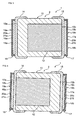
- a ceramic electronic component 1 has a ceramic element 2 and a pair of metal terminals 16 and 17.
- the ceramic element 2 has a ceramic element assembly 10 having a substantially rectangular parallelepiped shape which has been R-chamfered.
- the ceramic element assembly 10 has a plurality of laminated ceramic layers 11, and a plurality of first internal electrodes 12 having a substantially rectangular shape and a plurality of second internal electrodes 13 having a substantially rectangular shape disposed between the dielectric layers.
- the ceramic layer 11 is formed using a suitable ceramic.
- the ceramic layer 11 is formed using a dielectric ceramic, such as a BaTiO 3 ceramic.
- the ceramic electronic component 1 is a piezoelectric component
- the ceramic electronic component 1 is formed using a piezoelectric ceramic, such as a PZT ceramic.
- the ceramic electronic component 1 is a thermistor
- the ceramic electronic component 1 is formed using a semiconductor ceramic, such as a spinel ceramic.
- the plurality of first internal electrodes 12 and the plurality of second internal electrodes 13 are alternately laminated. Some of the plurality of the first internal electrodes 12 and some of the plurality of the second internal electrodes 13 are mutually interposed in the lamination direction of the first internal electrodes 12 and the second internal electrodes 13.
- the ceramic layer 11 is disposed between each of the first internal electrodes 12 and each of the second internal electrodes 13.
- each of the first and second internal electrodes 12 and 13 is suitably selected according to desired properties for the ceramic electronic component 1, kind of the ceramic layer 11, etc.
- each of the first and second internal electrodes 12 and 13 is formed of a metal, such as Cu, Ni, Ag, or Pd or an alloy, such as an Ag-Pd alloy.
- the first internal electrode 12 extends from a first end surface 10a of the ceramic element assembly 10.
- a first external electrode 14 is formed on the first end surface 10a.
- the first external electrode 14 is formed in such a manner as to cover the first end surface 10a.
- the first internal electrode 12 is electrically connected to the first external electrode 14.
- the second internal electrode 13 extends from a second end surface 10b of the ceramic element assembly 10.
- a second external electrode 15 is formed on the second end surface 10b.
- the second external electrode 15 is formed in such a manner as to cover the second end surface 10b.
- the second internal electrode 13 is electrically connected to the second external electrode 15.
- each of the first and second external electrodes 14 and 15 contains a sintered metal and glass.
- each of the first and second external electrodes 14 and 15 contains a metal such as Cu, Ni, Ag, or Pd, as a sintered metal, and glass.
- each of the first and second external electrodes 14 and 15 is obtained by sintering a mixture of powder of a metal, such as Cu, Ni, Ag, or Pd, or an alloy (e.g., Ag-Pd alloy) containing at least one of the metals as a main component and glass powder.
- a metal such as Cu, Ni, Ag, or Pd
- an alloy e.g., Ag-Pd alloy
- Each of the first and second external electrodes 14 and 15 does not have a plating film or the like formed thereon. Therefore, a sintered metal is exposed at the surface of the first and second external electrodes 14 and 15.
- Glass is added to the first and second external electrodes 14 and 15 for the purpose of increasing the bonding properties of the first and second external electrodes 14 and 15 for the ceramic element assembly 10 or increasing the sealing properties of the first and second external electrodes 14 and 15.
- glass is not an essential ingredient in the present invention, and each of the first and second external electrodes 14 and 15 may be formed of substantially only a sintered metal, for example.
- a first metal terminal 16 is bonded to the first external electrode 14.
- the first metal terminal 16 is formed into a substantially L shape.
- the first metal terminal 16 has a bonding portion 16a to be bonded to the first external electrode 14 and a mounting portion 16b to be mounted on a mounting substrate (not shown).
- a second metal terminal 17 is bonded.
- the second metal terminal 17 is formed into a substantially L shape. As shown in Fig. 2 , the second metal terminal 17 has a bonding portion 17a to be bonded to the second external electrode 15 and a mounting portion 17b to be mounted on a mounting substrate (not shown).
- Each of the first and second metal terminals 16 and 17 has terminal bodies 18a and 18b and plating films 19a and 19b.
- the plating films 19a and 19b are formed on the terminal bodies 18a and 18b, respectively. With the plating film 19a, the exposed portions of the terminal bodies 18a and 18b are covered.
- the plating films 19a and 19b have lower plating films 20a and 20b and upper plating films 21a and 21b, respectively.
- the lower plating films 20a and 20b are formed on the terminal bodies 18a and 18b, respectively.
- the upper plating films 21a and 21b are formed on the lower plating films 20a and 20b, respectively.
- Each of the lower plating films 20a and 20b and each of the upper plating films 21a and 21b may be formed of a plurality of plating films.
- the thickness of the terminal bodies 18a and 18b is preferably about 0.1 to about 0.5 mm.
- the thickness of the lower plating films 20a and 20b is preferably about 1.0 to about 5.0 ⁇ m.
- the thickness of the upper plating films 21a and 21b is preferably about 1.0 to about 5.0 ⁇ m.
- each of the terminal bodies 18a and 18b and each of the lower plating films 20a and 20b contain Ni, Fe, Cu, Ag, Cr, or an alloy containing at least one of the metals as a main component.
- Each of the terminal bodies 18a and 18b and each of the lower plating films 20a and 20b preferably contain Ni, Fe, Cr, or an alloy containing at least one of the metals as a main component.
- base materials of the terminal bodies 18a and 18b an Fe-42Ni alloy or a Fe-18Cr alloy is used, for example.
- the heat resistance of the first and second external electrodes 14 and 15 can be increased by forming each of the terminal bodies 18a and 18b and each of the lower plating films 20a and 20b using Ni, Fe, or Cr having a high melting point or an alloy containing at least one of the metals as a main component.
- the upper plating films 21a and 21b contain Sn, Ag, Au, or an alloy containing at least one of the metals as a main component.
- the upper plating films 21a and 21b contain Sn or an alloy containing Sn as a main component.
- the diffusion of metal from the first and second metal terminals 16 and 17 into the first and second external electrodes 14 and 15 can be accelerated.
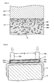
- Fig. 5 is a schematic cross section showing a bonding state of the first external electrode 14 with the first metal terminal 16.
- the first external electrode 14 and the first metal terminal 16 are directly diffusion-bonded when metals M1 to M3 in the first metal terminal 16 are diffused, on the atomic level, into the first external electrode 14.
- the second external electrode 15 and the second metal terminal 17 are directly diffusion-bonded when metals M1 to M3 in the second metal terminal 17 are diffused, on the atomic level, into the second external electrode 15.
- first and second external electrodes 14 and 15 and the first and second metal terminals 16 and 17 are directly diffusion-bonded, respectively, when both metals of the terminal bodies 18a and 18b and metals of the plating films 19a and 19b are diffused into the first and second external electrodes 14 and 15.
- Fig. 5 is a schematic view.
- the kind of the metals diffused into the first external electrode 14 are not limited to the three kinds.
- Reference character "G" in Fig. 5 represents glass.
- a ceramic green sheet, a conductive paste for internal electrode formation for forming the first and second internal electrodes 12 and 13, and a conductive paste for external electrode formation for forming the first and second external electrodes 14 and 15 are prepared.
- an organic binder or an organic solvent contained in the ceramic green sheet, the conductive paste for internal electrode formation, and the conductive paste for external electrode formation known organic binders and organic solvents can be used.
- an internal electrode pattern is formed by printing the conductive paste for internal electrode formation on the ceramic green sheet.
- the conductive paste for internal electrode formation can be printed by known methods, such as screen printing.
- a given number of ceramic green sheets on which the internal electrode pattern has been formed are laminated, and ceramic green sheets on which the internal electrode pattern is not formed are laminated above and below the ceramic green sheets, whereby a mother laminate is formed.
- the mother laminate may be pressed by isostatic pressing, for example, as required.
- the mother laminate is cut into a predetermined shape and dimensions to thereby obtain a raw ceramic laminate.
- the obtained raw ceramic laminate is fired.
- the firing temperature of the raw ceramic laminate is suitably determined according to the kind of the ceramic, the conductive paste for internal electrode formation, etc. Specifically, the firing temperature of the raw ceramic laminate is adjusted to be about 900 to about 1300°C, for example.
- the first and second external electrodes 14 and 15 are formed by applying the conductive paste for external electrode formation to both end surfaces of the fired ceramic laminate, and firing.
- the firing temperature of the conductive paste for external electrode formation is suitably determined according to the kind of the conductive paste for external electrode formation. Specifically, the firing temperature of the conductive paste for external electrode formation is adjusted to be about 700 to about 900°C, for example.
- the firing of the conductive paste for external electrode formation and the firing of the raw ceramic laminate are performed in air, in an N 2 atmosphere, or in an atmosphere of steam and N 2 , for example.
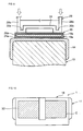
- the first and second metal terminals 16 and 17 are diffusion-bonded to the first and second external electrodes 14 and 15, respectively.
- a current is applied between a pair of bonding terminals 25a and 25b (welding rods) in a state where the pair of bonding terminals 25a and 25b are pressed against the first metal terminal 16 while the first external electrode 14 and the first metal terminal 16 are in contact with each other.
- the tips of the bonding terminals 25a and 25b, the first metal terminal 16, and the first external electrode 14 are heated.
- the first external electrode 14 contains a sintered metal and has gaps between metal particles. The gaps between metal particles are filled with glass.
- a current is applied between a pair of bonding terminals 25a and 25b (welding rods) in a state where the pair of bonding terminals 25a and 25b are pressed against the second metal terminal 17 while the second external electrode 15 and the second metal terminal 17 are in contact with each other.
- the tips of the bonding terminals 25a and 25b, the second metal terminal 17, and the second external electrode 15 are heated, and then the metal in the second metal terminal 17 is diffused into the second external electrode 15.
- the second external electrode 15 and the second metal terminal 17 are diffusion-bonded to each other.
- the bonding terminals 25a and 25b may be formed of tungsten, for example.
- the bonding conditions of the first and second metal terminals 16 and 17 are suitably determined according to the materials or the like of the first and second metal terminals 16 and 17 and the first and second external electrodes 14 and 15.
- the diffusion-bonding of the first and second metal terminals 16 and 17 is generally performed at a maximum current of about 200 to about 800A, at a welding time of about 300 to about 1000 msec, at a welding pressure of about 30 to about 50 N, and at a maximum temperature near the bonding portion of about 700 to about 900°C.
- the first and second metal terminals 16 and 17 are directly diffusion-bonded to the first and second external electrodes 14 and 15, respectively. Therefore, a solder and a bonding interface with a solder do not exist in the bonding portion, unlike the case where solder bonding is performed using a solder as disclosed in Patent Document 2.
- a ceramic electronic component having high reliability can be provided which is free from deterioration of the solder itself or deterioration of the bonding portion due to the generation of an intermetallic compound at the bonding interface under a high temperature environment or a thermal-cycle environment.
- a solder does not need to be prepared separately. Therefore, the material cost of the ceramic electronic component 1 can be reduced and the manufacturing processes of the ceramic electronic component 1 can be simplified.
- the heat resistance and thermal shock resistance of the ceramic electronic component 1 can increase, unlike the case where a high temperature solder containing no lead is used as disclosed in Patent Document 2.
- the plating films 19a and 19b are formed on the terminal bodies 18a and 18b. Therefore, the diffusion of metal from the first and second metal terminals 16 and 17 to the first and second external electrodes 14 and 15 can be accelerated. Moreover, when the plating films 19a and 19b are formed on the terminal bodies 18a and 18b, the mounting properties of the ceramic electronic component 1 for the mounting board can be improved.
- the first and second internal electrodes 12 and 13 are formed inside the ceramic element assembly 10.
- the first and second internal electrodes 12 and 13 are not essential constituent requirements.
- the ceramic element assembly 10 may contain a pair of ceramics in which no electrodes are formed.
- the first embodiment describes an example where a pair of bonding terminals 25a and 25b are used for the diffusion-bonding of the first and second external electrodes 14 and 15 with the first and second metal terminals 16 and 17, respectively, as shown in Fig. 6 .
- the bonding terminals used for the diffusion-bonding of the first and second external electrodes 14 and 15 with the first and second metal terminals 16 and 17, respectively, are not limited to the bonding terminals 25a and 25b.
- the first and second external electrodes 14 and 15 and the first and second metal terminals 16 and 17 may be diffusion-bonded using a bonding terminal 27 having a resistive portion 26.
- the bonding terminal 27 has a first terminal portion 28a and a second terminal portion 28b.
- the tip of the first terminal portion 28a and the tip of the second terminal portion 28b are connected by the resistive portion 26. Therefore, when a current is applied between the first terminal portion 28a and the second terminal portion 28b, the resistive portion 26 functions as a resistive element to generate heat.
- the resistive portion 26 When the resistive portion 26 is brought into contact with the first metal terminal 16, and a current is applied between the first and second terminal portions 28a and 28b, the first metal terminal 16 and the first external electrode 14 can be heated with the resistive portion 26 for diffusion-bonding.
- the junction terminal 27 can be formed of tungsten, for example, similarly as in the bonding terminals 25a and 25b of the first embodiment.
- the diffusion-bonding of the first and second external electrodes 14 and 15 with the first and second metal terminals 16 and 17 is generally performed at a maximum current of about 1200 to about 2000 A, at a welding time of about 500 to 1500 msec, at a welding pressure of about 60 to about 100 N, and at a maximum temperature near the bonding portion of about 700 to about 900°C.
- the first metal terminal 16 and the first external electrode 14 may be bonded to each other at a plurality of bonding portions C.
- the second metal terminal 17 and the second external electrode 15 may be bonded to each other at a plurality of bonding portions C.
- the first and second metal terminals 16 and 17 and the first and second external electrodes 14 and 15 are bonded to each other, respectively, at two bonding portions C.
- the bonding terminal 29 has the first and second terminal portions 28a and 28b, first and second resistive portions 30a and 30b, and a bonding portion 31.
- the first and second resistive portions 30a and 30b are pressed against the first metal terminal 16.
- the resistive portions 30a and 30b generate heat.
- the bonding portion C the first metal terminal 16 and the first external electrode 14 are heated for diffusion-bonding.
- a stress can be dissipated which generates in the ceramic element assembly 10 or the like when the first and second metal terminals 16 and 17 and the first and second external electrodes 14 and 15 are bonded to each other, respectively, or during cooling after bonding. Therefore, the development of cracks in the ceramic element assembly 10 or the like can be effectively suppressed.
- Figs. 8 , 10 , and 12 represent a bonding portion of the first and second metal terminals 16 and 17 with the first and second external electrodes 14 and 15, respectively, and indentation on the front surface of the metal terminal, and do not represent the cross section of the members.
- Fig. 10 is a side view of the ceramic electronic component 1 according to a third embodiment.
- the first metal terminal 16 has a plurality of filament-like terminal portions 32 disposed in parallel to each other.
- the second metal terminal 17 also has two filament-like terminal portions 32 disposed in parallel to each other in this embodiment similarly as the first metal terminal 16.
- the tip of each of the terminal portion 32 of the first and second metal terminals 16 and 17 is diffusion-bonded to the first and second external electrodes 14 and 15.
- the diffusion-bonding method of the first and second metal terminals 16 and 17 with the first and second external electrodes 14 and 15, respectively, in the third embodiment there is no limitation regarding the diffusion-bonding method of the first and second metal terminals 16 and 17 with the first and second external electrodes 14 and 15, respectively, in the third embodiment.
- the diffusion-bonding of the first and second metal terminals 16 and 17 with the first and second external electrodes 14 and 15, respectively, in the third embodiment can be achieved by the bonding terminal 27.
- the number of the terminal portion 32 of the first and second metal terminals 16 and 17 is not limited to two.
- three terminal portions 32 may be provided.
- a stress generated in the ceramic element assembly 10 or the like during bonding or cooling can be dissipated more effectively. Therefore, the development of cracks in the ceramic element assembly 10 or the like can be suppressed more effectively.
- the diffusion-bonding method of the first and second metal terminals 16 and 17 with the first and second external electrodes 14 and 15, respectively, in the fourth embodiment there is no limitation regarding the diffusion-bonding method of the first and second metal terminals 16 and 17 with the first and second external electrodes 14 and 15, respectively, in the fourth embodiment.
- the diffusion-bonding of the first metal terminal 16 and the first external electrode 14 in the fourth embodiment can be achieved using the pair of the bonding terminals 25a and 25b.
- the diffusion-bonding of the terminal portion 32 located outside and the first external electrode 14 can be achieved by heat generation of the second bonding terminals 25a and 25b.
- Fig. 14 is a cross section showing a ceramic electronic component in a second modified example. As shown in Fig. 14 , an anti-corrosion film 35 that covers an exposed portion of the outer surface the first and second external electrodes 14 and 15 may be provided. Thus, oxidation of the first and second metal terminals 16 and 17 can be suppressed.
- the anti-corrosion film 35 is not limited.
- the anti-corrosion film 35 may be an imidazole or benzotriazole organic coating or a plating film, such as an Sn plating film.
- a heat source in the diffusion-bonding of the metal terminals 16 and 17 and the external electrodes 14 and 15, respectively there is no limitation regarding a heat source in the diffusion-bonding of the metal terminals 16 and 17 and the external electrodes 14 and 15, respectively.
- a laser beam may be emitted from the metal terminal side in a state where the metal terminals 16 and 17 are in contact with the external electrodes 14 and 15, respectively. In such a case, the output of the laser is adjusted so that the external electrodes 14 and 15 do not melt.
- a paste in which Cu powder having an average particle diameter of about 1.8 ⁇ m and glass powder having an average particle diameter of about 2 ⁇ m were mixed with a weight ratio of about 9:1 was applied to both ends of the ceramic element assembly 10, and the resultant was fired at about 88°C for about 1 hour, thereby forming the first and second external electrodes 14 and 15.
- first external electrode 14 and the first metal terminal 16 and the second external electrode 15 and the second metal terminal 17 were brought into contact with each other, and were diffusion-bonded on the conditions of a maximum current of about 280 A and a welding time of about 600 msec in a state where they are pressed against each other at a welding pressure of about 40 N.
- the first external electrode 14 and the first metal terminal 16 and the second external electrode 15 and the second metal terminal 17 were bonded to each other using an Sn-0.7Cu solder.
- Each of the diffusion-bonded ceramic electronic component and the soldered ceramic electronic component was subjected to a reflow heat resistance test, a high temperature load test, and a thermal shock cycle test.
- the reflow heat resistance test was performed by passing the ceramic electronic components through an about 230°C reflow furnace a plurality of times, and visually observing floating of the ceramic element assembly 10.
- a high temperature load test measured the bond strength between the first and second external electrodes 14 and 15 and the first and second metal terminals 16 and 17, respectively after the ceramic electronic component was allowed to stand in an about 175°C atmosphere for about 1000 hours. Moreover, the diffusion-bonded ceramic electronic component and the soldered ceramic electronic component before the high temperature load test were measured for the bond strength between the first and second external electrodes 14 and 15 and the first and second metal terminals 16 and 17, respectively.
- the bond strength was measured as follows: the center of the ceramic element assembly was pressed in the direction in parallel to the first and second metal terminals and in parallel to the substrate in a state where the first and second metal terminals of the ceramic electronic component are fixed on the substrate, a load when the first and second metal terminals were disconnected was measured using a push-pull gage (tradename: RX-100, manufactured by Aikoh Engineering Co., Ltd.), and the measured load was used as the bond strength.
- the bond strength decreased as high as about 60% by the high temperature load test, and in contrast, in the diffusion-bonded ceramic electronic component, the bond strength decreased as low as about 10% by the high temperature load test.
- the results show that a higher heat resistance can be obtained in the case where the first and second metal terminals 16 and 17 and the first and second external electrodes 14 and 15 were diffusion-bonded, respectively, compared with the case where they were soldered.
- a thermal shock cycle test measured the bond strength between the first and second external electrodes 14 and 15 and the first and second metal terminals 16 and 17, respectively, by the above-described procedure after a cycle in which the ceramic electronic component was allowed to stand at a temperature of about 55°C for about 30 minutes, and then at a temperature of about 125°C for about 30 minutes was repeated about 3000 times. Moreover, the diffusion-bonded ceramic electronic component and the soldered ceramic electronic component before the thermal shock cycle test were measured for the bond strength between the first and second external electrodes 14 and 15 and the first and second metal terminals 16 and 17, respectively, by the above-described procedure.
- the bond strength decreased as high as about 80% by the thermal shock cycle test, and in contrast, in the diffusion-bonded ceramic electronic component, the reduction in bond strength by the thermal shock cycle test was not observed.
- the results also show that a higher thermal shock resistance can be obtained in the case where the first and second metal terminals 16 and 17 and the first and second external electrodes 14 and 15 were diffusion-bonded, respectively, compared with the case where they were soldered.
- the external electrodes and the metal terminals are diffusion-bonded by heating in a state where the external electrodes and the metal terminals are brought into contact with each other.
- Figs. 15 to 21 the first and second metal terminals 16 and 17 are brought into contact with the external electrodes 14 and 15 of the ceramic element 2 described above, respectively, and terminals for diffusion-bonding 41 and 42 are brought into contact with the metal terminals 16 and 17 from the outer surface, followed by heating.
- the metal terminals 16 and 17 are diffusion-bonded to the external electrodes 14 and 15, respectively.
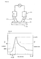
- Fig. 15 schematically shows the terminals for diffusion-bonding 41 and 42, and suitable terminals according to a heating system are used.
- the terminal for diffusion-bonding 41 for heating by a pulse heat system may be brought into contact with the outer surface of the metal terminal 16 in a portion where the metal terminal 16 is brought into contact with the external electrode 14.
- a pulse current is applied to the terminal for diffusion-bonding 41 as indicated by the arrow of Fig. 16 to heat the metal terminal 16.
- Fig. 17 is a view showing a relationship between a period of time while a pulse current is being applied and the temperature of the metal terminal 16.
- One division of the abscissa of Fig. 17 is about 0.2 second. It is revealed that the temperature of the metal terminal 16 increases as the application of a pulse current.
- the metal terminal 16 in order to achieve diffusion-bonding, when the metal terminal 16 is copper or when the external electrode 14 is copper, it is necessary to heat the same up to about 400°C as shown in Fig. 17 .
- the metal terminal 16 can be diffusion-bonded to the external electrode 14.
- a current is applied as shown in Fig. 17 , cracks developed in the ceramic element assembly 10 in 8 ceramic elements 2 out of 10 ceramic elements 2.
- the present inventors found that the development of cracks was suppressed when a current is applied a plurality of times while stopping the current application until the temperature reaches about 400°C, without heating from normal temperature to about 400°C at one time. More specifically, it is revealed that when the metal terminal 16 is heated to about 230°C by a first application of a pulse current, the application is once stopped, and then a pulse current is applied again about 0.3 second later to increase the temperature of the metal terminal 16 to about 400°C as shown in Fig. 18 , cracks hardly develops in the ceramic element assembly 10. According to the experiment, the development of cracks was not observed in 10 ceramic elements.
- the difficulty of the development of cracks in the ceramic element assembly 10 when a current is applied a plurality of times as shown in Fig. 18 is possibly based on the reduction in stress in the ceramic element assembly 10 due to stopping of the heating after heated for a given time to about 230°C.
- a current is applied a plurality of times when the metal terminals 16 and 17 are heated for diffusion-bonding.
- a current is applied twice, but a current is applied 3 times or more until the temperature reaches the maximum temperature by heating.
- a temperature at which cracks are likely to develop in the ceramic element assembly 10 is measured by manufacturing the ceramic element 2, and then heating the metal terminal 16 by one current application. It is preferable to start a second current application after a current is applied to the metal terminal 16 so as not to reach the measured temperature, and then the current application is stopped.
- the method shows a temperature at which the current application needs to stop, e.g., about 230°C in Fig. 18 .
- the heating method is not limited to the heating method by a pulse heat system, and a heating method by a parallel gap system shown in Fig. 19 may be employed.
- the terminal for diffusion-bonding 41 having a pair of probes 41a and 41b is used.
- the probes 41a and 41b are brought into contact with the metal terminal 16 at a given gap.
- a current is applied as indicated by the arrow of Fig. 19 to heat the metal terminal 16 by contact resistance.
- the heating method by a parallel gap system the development of cracks in the ceramic element assembly can be suppressed by applying a current a plurality of times.
- the current application may be performed a plurality of times to reach the maximum temperature by heating.
- a current may be applied in such a manner as to reduce a temperature decrease rate at the time of temperature decrease in which a temperature decreases from the maximum temperature to normal temperature. This will be described with reference to Figs. 20 and 21 .
- Fig. 20 the metal terminal 16 was heated using the ceramic element assembly 10 having a composition different from the case of Fig. 17 by a heating method by a parallel gap heating system.
- a current was applied in a period of time from normal temperature to A 0 of Fig. 20 to increase the temperature of the metal terminal 16 to about 200°C for diffusion-bonding.
- the welding time A 0 is about 0.2 second.
- One division of the abscissa of Figs. 20 and 21 is about 0.1 second.
- the current application was stopped before the temperature reaches about 200°C as the maximum temperature. After reaching the maximum temperature, the temperature of the metal terminal 16 naturally decreases. Therefore, the temperature decrease rate is relatively high. In this case, the development of cracks due to shrinkage of the ceramic element assembly was sometimes observed in a period of temperature decrease.
- a current was applied only in a period of A 0 to increase the temperature to the maximum temperature by heating similarly as in Fig. 20 , and then a smaller current was applied only in a period of A 1 in a period of temperature decrease to reduce a temperature decrease rate.
- the temperature decrease rate decreases to reduce a temperature gradient in a period of temperature decrease. Therefore, the development of cracks due to shrinkage was not observed in the ceramic element assembly.
- the development of cracks in the ceramic element assembly 10 can be suppressed by heating also in a period of temperature decrease to decrease the temperature decrease rate.
- the terminal for diffusion-bonding into contact with the metal terminal, and apply a current a plurality of times when diffusion-bonding is performed by heating in a state where the external electrode and the metal terminal are brought into contact with each other.
- the plurality of current applications may be performed throughout the entire diffusion-bonding process. As shown in Fig. 18 , the current application may be performed a plurality of times in a process until a temperature reaches the maximum temperature. As shown in Fig. 21 , the current application may be performed a plurality of times before and after reaching the maximum temperature.
Landscapes
- Engineering & Computer Science (AREA)
- Power Engineering (AREA)
- Microelectronics & Electronic Packaging (AREA)
- Manufacturing & Machinery (AREA)
- Chemical & Material Sciences (AREA)
- Ceramic Engineering (AREA)
- Inorganic Chemistry (AREA)
- Ceramic Capacitors (AREA)
- Fixed Capacitors And Capacitor Manufacturing Machines (AREA)
- Ceramic Products (AREA)
Abstract
Description
- The present invention relates to a ceramic electronic component, and particularly to a ceramic electronic component having external electrodes and metal terminals electrically connected to the external electrodes, and a method for manufacturing the same.
- In general, ceramic electronic components, such as a ceramic capacitor, are placed in an environment in which they are easily subjected to a mechanical stress in mounting or during use in many cases. For example, a stress is applied to a ceramic electronic component in some cases when a wiring board on which the ceramic electronic component has been mounted bends or when the temperature of the wiring board changes to change the volume of a wiring board. Thus, when a stress is applied to a ceramic electronic component, fractures or cracks may occur in ceramic element assemblies. In view of such problems,
Patent Document 1 has proposed a method for bonding a metal terminal to an external electrode of a ceramic capacitor element using a solder containing lead in a proportion of about 80% or more and about 98% or lower, for example. - However, in recent years, the restriction of the use of certain hazardous substances in electrical and electronic equipment has rapidly proceeded as typified by the European RoHS directive or the like, and the use of a solder containing lead is becoming less acceptable. In view of this, in
Patent Document 2, the use of a Sn-Sb high temperature solder for bonding terminal electrodes of electronic components and metal terminals, for example, has been proposed. - Patent-Document 1: Japanese Unexamined Patent Application Publication No.
4-259205 - Patent Document 2: Japanese Unexamined Patent Application Publication No.
2003-303736 - However, as disclosed in
Patent Documents - Accordingly, it is an object of the present invention to provide a ceramic electronic component having highly reliable metal terminal bonding, and a method for manufacturing the same.
- A ceramic electronic component according to preferred embodiments of the present invention has a ceramic element assembly, an external electrode, and a metal terminal. The external electrode is formed on the surface of the ceramic element assembly. The external electrode contains a sintered metal. The metal terminal is electrically connected to the external electrode. In the ceramic electronic component according to preferred embodiments of the present invention, the external electrode and the metal terminal are directly diffusion-bonded by diffusion of metal in the metal terminal into the external electrode.
- According to a specific aspect of the present invention, the metal terminal has a terminal body and a plating film formed on the terminal body, in which the external electrode and the metal terminal are directly diffusion-bonded by diffusion of both metal in the terminal body and metal in the plating film into the external electrode.
- According to another specific aspect of the present invention, the plating film has a lower plating film formed on the terminal body and an upper plating film formed on the lower plating film.
- According to another specific aspect of the present invention, the terminal body and the lower plating film each contain Ni, Fe, Cu, Ag, Cr, or an alloy containing at least one of the metals as a main component and the upper plating film contains Sn, Ag, Au, or an alloy containing at least one of the metals as a main component.
- According to still another specific aspect of the present invention, the external electrode contains Cu, Ni, Ag, Pd, or an alloy containing at least one of the metals as a main component.
- According to still another specific aspect of the present invention, the ceramic electronic component has an anti-corrosion film that covers an exposed portion of the outer surface of the external electrode.
- According to still another specific aspect of the present invention, the external electrode and the metal terminal are diffusion-bonded at a plurality of places.
- According to still another specific aspect of the present invention, the metal terminal is diffusion-bonded to the external electrode and has a plurality of filament-like terminal portions disposed in parallel to each other.
- According to still another specific aspect of the present invention, the ceramic element assembly has a first end surface and a second end surface that are mutually opposite, the external electrode has a first external electrode that covers the first end surface and a second external electrode that covers the second end surface, and the metal terminal has a first metal terminal electrically connected to the first external electrode and a second metal terminal electrically connected to the second external electrode.
- According to still another specific aspect of the present invention, the surface of the external electrode is not covered with a plating film.
- A method for manufacturing a ceramic electronic component according to preferred embodiments of the present invention relates to a method for manufacturing the ceramic electronic component according to preferred embodiments of the present invention. The method for manufacturing a ceramic electronic component according to preferred embodiments of the present invention includes heating the external electrode and the metal terminal while being contacted to diffuse metal in the metal terminal into the external electrode for direct diffusion-bonding of the external electrode and the metal terminal.
- According to a specific aspect of the method for manufacturing a ceramic electronic, a terminal for diffusion-bonding is brought into contact with the metal terminal, and applying a current a plurality of times upon heating the external electrode and the metal terminal while being contacted for diffusion-bonding thereof. Preferably, the metal terminal is heated to a temperature range in which cracks do not occur in the ceramic element assembly at a first current application among the plurality of current applications.
- In the ceramic electronic component according to preferred embodiments of the present invention, the external electrode and the metal terminal are directly diffusion-bonded by diffusion of the metal in the metal terminal into the external electrode, and thus metal terminal bonding excellent in heat resistance or reliability can be achieved.
- Other features, elements, characteristics and advantages of the present invention will become more apparent from the following detailed description of preferred embodiments of the present invention with reference to the attached drawings.
-
-
Fig. 1 is a perspective view of a ceramic electronic component according to a first embodiment of the present invention; -
Fig. 2 is a view as viewed along direction of arrow II-II inFig. 1 ; -
Fig. 3 is a view as viewed along direction of arrow III-III inFig. 2 ; -
Fig. 4 is a view as viewed along direction of arrow IV-IV inFig. 2 ; -
Fig. 5 is a schematic cross section showing a bonding state of a first external electrode with a first metal terminal; -
Fig. 6 is a cross section showing a diffusion-bonding process of the first external electrode with the first metal terminal according to a first embodiment; -
Fig. 7 is a cross section showing a diffusion-bonding process of the first external electrode with the first metal terminal according to a first modified example; -
Fig. 8 is a side view of a ceramic electronic component according to a second embodiment; -
Fig. 9 is a cross section showing a diffusion-bonding process of the first external electrode with the first metal terminal according to a second embodiment; -
Fig. 10 is a side view of a ceramic electronic component according to a third embodiment; -
Fig. 11 is a cross section showing a diffusion-bonding process of the first external electrode with the first metal terminal according to a third embodiment; -
Fig. 12 is a side view of a ceramic electronic component according to a fourth embodiment; -
Fig. 13 is a cross section showing a diffusion-bonding process of the first external electrode with the first metal terminal according to a fourth embodiment; -
Fig. 14 is a cross section of a ceramic electronic component according to a second modified example; -
Fig. 15 is a schematic perspective view showing a diffusion-bonding process; -
Fig. 16 is a schematic front view showing a diffusion-bonding method by a pulse heat system; -
Fig. 17 is a view showing temperature changes of the metal terminal when a current is applied 1 time upon diffusion-bonding by a pulse heat system in a modified example of the manufacturing method according to preferred embodiments of the present invention; -
Fig. 18 is a view showing temperature changes of the metal terminal when a current is applied a plurality of times upon diffusion-bonding by a pulse heat system in a modified example of the manufacturing method according to preferred embodiments of the present invention; -
Fig. 19 is a schematic front view showing a heating method by a parallel gap system according to another modified example of the method for manufacturing a ceramic electronic component according to preferred embodiments of the present invention; -
Fig. 20 is a view showing a relationship between an applied current when heating is performed by a parallel gap system upon diffusion-bonding and temperature changes of the metal terminal in the method for manufacturing a ceramic electronic component according to preferred embodiments of the present invention; and -
Fig. 21 is a view showing a relationship between an applied current, when heating is performed by a parallel gap system upon diffusion-bonding and a current is applied also in a period of temperature decrease, and temperature changes of the metal terminal in the method for manufacturing a ceramic electronic component according to preferred embodiments of the present invention. - As shown in
Figs. 1 and 2 , a ceramicelectronic component 1 has aceramic element 2 and a pair ofmetal terminals ceramic element 2 has aceramic element assembly 10 having a substantially rectangular parallelepiped shape which has been R-chamfered. As shown inFig. 2 , theceramic element assembly 10 has a plurality of laminatedceramic layers 11, and a plurality of firstinternal electrodes 12 having a substantially rectangular shape and a plurality of secondinternal electrodes 13 having a substantially rectangular shape disposed between the dielectric layers. - The
ceramic layer 11 is formed using a suitable ceramic. For example, when the ceramicelectronic component 1 is a capacitor, theceramic layer 11 is formed using a dielectric ceramic, such as a BaTiO3 ceramic. For example, when the ceramicelectronic component 1 is a piezoelectric component, the ceramicelectronic component 1 is formed using a piezoelectric ceramic, such as a PZT ceramic. For example, when the ceramicelectronic component 1 is a thermistor, the ceramicelectronic component 1 is formed using a semiconductor ceramic, such as a spinel ceramic. - The plurality of first
internal electrodes 12 and the plurality of secondinternal electrodes 13 are alternately laminated. Some of the plurality of the firstinternal electrodes 12 and some of the plurality of the secondinternal electrodes 13 are mutually interposed in the lamination direction of the firstinternal electrodes 12 and the secondinternal electrodes 13. Theceramic layer 11 is disposed between each of the firstinternal electrodes 12 and each of the secondinternal electrodes 13. - The material of each of the first and second
internal electrodes electronic component 1, kind of theceramic layer 11, etc. For example, each of the first and secondinternal electrodes - As shown in
Figs. 2 and4 , the firstinternal electrode 12 extends from afirst end surface 10a of theceramic element assembly 10. On thefirst end surface 10a, a firstexternal electrode 14 is formed. Specifically, the firstexternal electrode 14 is formed in such a manner as to cover thefirst end surface 10a. The firstinternal electrode 12 is electrically connected to the firstexternal electrode 14. - As shown in
Figs. 2 and3 , the secondinternal electrode 13 extends from asecond end surface 10b of theceramic element assembly 10. On thesecond end surface 10b, a secondexternal electrode 15 is formed. Specifically, the secondexternal electrode 15 is formed in such a manner as to cover thesecond end surface 10b. The secondinternal electrode 13 is electrically connected to the secondexternal electrode 15. - In this embodiment, each of the first and second
external electrodes external electrodes external electrodes external electrodes external electrodes - Glass is added to the first and second
external electrodes external electrodes ceramic element assembly 10 or increasing the sealing properties of the first and secondexternal electrodes external electrodes - As shown in
Figs. 1 and 2 , afirst metal terminal 16 is bonded to the firstexternal electrode 14. Thefirst metal terminal 16 is formed into a substantially L shape. Thefirst metal terminal 16 has abonding portion 16a to be bonded to the firstexternal electrode 14 and a mountingportion 16b to be mounted on a mounting substrate (not shown). - To the second
external electrode 15, asecond metal terminal 17 is bonded. Thesecond metal terminal 17 is formed into a substantially L shape. As shown inFig. 2 , thesecond metal terminal 17 has abonding portion 17a to be bonded to the secondexternal electrode 15 and a mountingportion 17b to be mounted on a mounting substrate (not shown). - Each of the first and
second metal terminals terminal bodies films films terminal bodies plating film 19a, the exposed portions of theterminal bodies - The plating
films lower plating films upper plating films lower plating films terminal bodies upper plating films lower plating films lower plating films upper plating films - The thickness of the
terminal bodies lower plating films upper plating films - According to this embodiment, each of the
terminal bodies lower plating films terminal bodies lower plating films terminal bodies - The heat resistance of the first and second
external electrodes terminal bodies lower plating films - The
upper plating films upper plating films - By the formation of the
upper plating films second metal terminals external electrodes -
Fig. 5 is a schematic cross section showing a bonding state of the firstexternal electrode 14 with thefirst metal terminal 16. As shown inFig. 5 , in this embodiment, the firstexternal electrode 14 and thefirst metal terminal 16 are directly diffusion-bonded when metals M1 to M3 in thefirst metal terminal 16 are diffused, on the atomic level, into the firstexternal electrode 14. Similarly, the secondexternal electrode 15 and thesecond metal terminal 17 are directly diffusion-bonded when metals M1 to M3 in thesecond metal terminal 17 are diffused, on the atomic level, into the secondexternal electrode 15. Specifically, the first and secondexternal electrodes second metal terminals terminal bodies films external electrodes -
Fig. 5 is a schematic view. The kind of the metals diffused into the firstexternal electrode 14 are not limited to the three kinds. Reference character "G" inFig. 5 represents glass. - Next, processes for manufacturing the ceramic
electronic component 1 will be described in detail. - First, a ceramic green sheet, a conductive paste for internal electrode formation for forming the first and second
internal electrodes external electrodes - Next, an internal electrode pattern is formed by printing the conductive paste for internal electrode formation on the ceramic green sheet. The conductive paste for internal electrode formation can be printed by known methods, such as screen printing.
- Next, a given number of ceramic green sheets on which the internal electrode pattern has been formed are laminated, and ceramic green sheets on which the internal electrode pattern is not formed are laminated above and below the ceramic green sheets, whereby a mother laminate is formed. The mother laminate may be pressed by isostatic pressing, for example, as required.
- Next, the mother laminate is cut into a predetermined shape and dimensions to thereby obtain a raw ceramic laminate. The obtained raw ceramic laminate is fired. The firing temperature of the raw ceramic laminate is suitably determined according to the kind of the ceramic, the conductive paste for internal electrode formation, etc. Specifically, the firing temperature of the raw ceramic laminate is adjusted to be about 900 to about 1300°C, for example.
- Next, the first and second
external electrodes - Next, the first and
second metal terminals external electrodes Fig. 6 , a current is applied between a pair ofbonding terminals bonding terminals first metal terminal 16 while the firstexternal electrode 14 and thefirst metal terminal 16 are in contact with each other. Thus, the tips of thebonding terminals first metal terminal 16, and the firstexternal electrode 14 are heated. Here, in this embodiment, the firstexternal electrode 14 contains a sintered metal and has gaps between metal particles. The gaps between metal particles are filled with glass. Thus, when the tips of thebonding terminals first metal terminal 16, and the firstexternal electrode 14 are heated, diffusion of the metal in thefirst metal terminal 16 into the metal particles of the firstexternal electrode 14 is accelerated. As a result, thefirst metal terminal 16 and the firstexternal electrode 14 are diffusion-bonded to each other. - Similarly, a current is applied between a pair of
bonding terminals bonding terminals second metal terminal 17 while the secondexternal electrode 15 and thesecond metal terminal 17 are in contact with each other. Thus, the tips of thebonding terminals second metal terminal 17, and the secondexternal electrode 15 are heated, and then the metal in thesecond metal terminal 17 is diffused into the secondexternal electrode 15. As a result, the secondexternal electrode 15 and thesecond metal terminal 17 are diffusion-bonded to each other. - There is no limitation regarding the material of the
bonding terminals bonding terminals second metal terminals second metal terminals external electrodes second metal terminals - As described above, in this embodiment, the first and
second metal terminals external electrodes Patent Document 2. Thus, a ceramic electronic component having high reliability can be provided which is free from deterioration of the solder itself or deterioration of the bonding portion due to the generation of an intermetallic compound at the bonding interface under a high temperature environment or a thermal-cycle environment. - In this embodiment, a solder does not need to be prepared separately. Therefore, the material cost of the ceramic
electronic component 1 can be reduced and the manufacturing processes of the ceramicelectronic component 1 can be simplified. - When the first and
second metal terminals external electrodes electronic component 1 can increase, unlike the case where a high temperature solder containing no lead is used as disclosed inPatent Document 2. - In this embodiment, the plating
films terminal bodies second metal terminals external electrodes films terminal bodies electronic component 1 for the mounting board can be improved. - In this embodiment, a description is given for the case where the first and second
internal electrodes ceramic element assembly 10. In the present invention, the first and secondinternal electrodes ceramic element assembly 10 may contain a pair of ceramics in which no electrodes are formed. - Hereinafter, further embodiments and modified examples of the present invention will be described. In the following description, members having functions substantially common with those of the first embodiment are denoted with the same reference numerals, and thus descriptions thereof are omitted.
- The first embodiment describes an example where a pair of
bonding terminals external electrodes second metal terminals Fig. 6 . The bonding terminals used for the diffusion-bonding of the first and secondexternal electrodes second metal terminals bonding terminals - For example, as shown in
Fig. 7 , the first and secondexternal electrodes second metal terminals bonding terminal 27 having aresistive portion 26. Specifically, thebonding terminal 27 has a firstterminal portion 28a and a secondterminal portion 28b. The tip of the firstterminal portion 28a and the tip of the secondterminal portion 28b are connected by theresistive portion 26. Therefore, when a current is applied between the firstterminal portion 28a and the secondterminal portion 28b, theresistive portion 26 functions as a resistive element to generate heat. - When the
resistive portion 26 is brought into contact with thefirst metal terminal 16, and a current is applied between the first and secondterminal portions first metal terminal 16 and the firstexternal electrode 14 can be heated with theresistive portion 26 for diffusion-bonding. - The
junction terminal 27 can be formed of tungsten, for example, similarly as in thebonding terminals - In this modified example, the diffusion-bonding of the first and second
external electrodes second metal terminals - As shown in
Fig. 8 , thefirst metal terminal 16 and the firstexternal electrode 14 may be bonded to each other at a plurality of bonding portions C. Similarly, thesecond metal terminal 17 and the secondexternal electrode 15 may be bonded to each other at a plurality of bonding portions C. Specifically, in this embodiment, the first andsecond metal terminals external electrodes - When the
first metal terminal 16 and the firstexternal electrode 14 are bonded to each other at two bonding portions C, thefirst metal terminal 16 and the firstexternal electrode 14 can be bonded to each other using abonding terminal 29 shown inFig. 9 . Thebonding terminal 29 has the first and secondterminal portions resistive portions 30a and 30b, and abonding portion 31. When thefirst metal terminal 16 and the firstexternal electrode 14 are bonded to each other, the first and secondresistive portions 30a and 30b are pressed against thefirst metal terminal 16. When a current is applied between the first and secondterminal portions resistive portions 30a and 30b generate heat. As a result, in the bonding portion C; thefirst metal terminal 16 and the firstexternal electrode 14 are heated for diffusion-bonding. - As in this embodiment, by providing the plurality of the bonding portions C of the first and
second metal terminals external electrodes ceramic element assembly 10 or the like when the first andsecond metal terminals external electrodes ceramic element assembly 10 or the like can be effectively suppressed. - The hatched portions of
Figs. 8 ,10 , and12 represent a bonding portion of the first andsecond metal terminals external electrodes -
Fig. 10 is a side view of the ceramicelectronic component 1 according to a third embodiment. As shown inFig. 10 , thefirst metal terminal 16 has a plurality of filament-liketerminal portions 32 disposed in parallel to each other. Although not shown, thesecond metal terminal 17 also has two filament-liketerminal portions 32 disposed in parallel to each other in this embodiment similarly as thefirst metal terminal 16. The tip of each of theterminal portion 32 of the first andsecond metal terminals external electrodes - Thus, by providing the plurality of the
terminal portions 32 to the first andsecond metal terminals ceramic element assembly 10 or the like when the first andsecond metal terminals external electrodes ceramic element assembly 10 or the like can be effectively suppressed. - There is no limitation regarding the diffusion-bonding method of the first and
second metal terminals external electrodes Fig. 11 , the diffusion-bonding of the first andsecond metal terminals external electrodes bonding terminal 27. - The number of the
terminal portion 32 of the first andsecond metal terminals Fig. 12 , threeterminal portions 32 may be provided. In an example shown inFig. 12 , since four bonding portions C are provided, a stress generated in theceramic element assembly 10 or the like during bonding or cooling can be dissipated more effectively. Therefore, the development of cracks in theceramic element assembly 10 or the like can be suppressed more effectively. - There is no limitation regarding the diffusion-bonding method of the first and
second metal terminals external electrodes Fig. 13 , the diffusion-bonding of thefirst metal terminal 16 and the firstexternal electrode 14 in the fourth embodiment can be achieved using the pair of thebonding terminals terminal portion 32 located outside and the firstexternal electrode 14 can be achieved by heat generation of thesecond bonding terminals -
Fig. 14 is a cross section showing a ceramic electronic component in a second modified example. As shown inFig. 14 , ananti-corrosion film 35 that covers an exposed portion of the outer surface the first and secondexternal electrodes second metal terminals - The
anti-corrosion film 35 is not limited. For example, theanti-corrosion film 35 may be an imidazole or benzotriazole organic coating or a plating film, such as an Sn plating film. - There is no limitation regarding a heat source in the diffusion-bonding of the
metal terminals external electrodes metal terminals external electrodes external electrodes - A paste in which Cu powder having an average particle diameter of about 1.8 µm and glass powder having an average particle diameter of about 2 µm were mixed with a weight ratio of about 9:1 was applied to both ends of the
ceramic element assembly 10, and the resultant was fired at about 88°C for about 1 hour, thereby forming the first and secondexternal electrodes - An about 1.0 µm thick Ni plating film and an about 2.0 µm thick Sn plating film were successively formed on an about 0.1 mm thick metal plate formed of an Fe-42Ni alloy, thereby manufacturing the first and
second metal terminals Fig. 10 . - Next, the first
external electrode 14 and thefirst metal terminal 16 and the secondexternal electrode 15 and thesecond metal terminal 17 were brought into contact with each other, and were diffusion-bonded on the conditions of a maximum current of about 280 A and a welding time of about 600 msec in a state where they are pressed against each other at a welding pressure of about 40 N. - As a comparative example, the first
external electrode 14 and thefirst metal terminal 16 and the secondexternal electrode 15 and thesecond metal terminal 17 were bonded to each other using an Sn-0.7Cu solder. - Each of the diffusion-bonded ceramic electronic component and the soldered ceramic electronic component was subjected to a reflow heat resistance test, a high temperature load test, and a thermal shock cycle test.
- The reflow heat resistance test was performed by passing the ceramic electronic components through an about 230°C reflow furnace a plurality of times, and visually observing floating of the
ceramic element assembly 10. - Floating of the
ceramic element assembly 10 was not observed in the diffusion-bonded ceramic electronic component even when it was made to pass through thereflow furnace 10 times. In contrast, floating of theceramic element assembly 10 was observed in the soldered ceramic electronic component after it was made to pass through the reflow furnace 6 times. The results show that a higher heat resistance can be obtained in the case where the first andsecond metal terminals external electrodes - A high temperature load test measured the bond strength between the first and second
external electrodes second metal terminals external electrodes second metal terminals - The bond strength was measured as follows: the center of the ceramic element assembly was pressed in the direction in parallel to the first and second metal terminals and in parallel to the substrate in a state where the first and second metal terminals of the ceramic electronic component are fixed on the substrate, a load when the first and second metal terminals were disconnected was measured using a push-pull gage (tradename: RX-100, manufactured by Aikoh Engineering Co., Ltd.), and the measured load was used as the bond strength.
- In the soldered ceramic electronic component, the bond strength decreased as high as about 60% by the high temperature load test, and in contrast, in the diffusion-bonded ceramic electronic component, the bond strength decreased as low as about 10% by the high temperature load test. The results also show that a higher heat resistance can be obtained in the case where the first and
second metal terminals external electrodes - A thermal shock cycle test measured the bond strength between the first and second
external electrodes second metal terminals
in which the ceramic electronic component was allowed to stand at a temperature of about 55°C for about 30 minutes, and then at a temperature of about 125°C for about 30 minutes was repeated about 3000 times. Moreover, the diffusion-bonded ceramic electronic component and the soldered ceramic electronic component before the thermal shock cycle test were measured for the bond strength between the first and secondexternal electrodes second metal terminals - In the soldered ceramic electronic component, the bond strength decreased as high as about 80% by the thermal shock cycle test, and in contrast, in the diffusion-bonded ceramic electronic component, the reduction in bond strength by the thermal shock cycle test was not observed. The results also show that a higher thermal shock resistance can be obtained in the case where the first and
second metal terminals external electrodes - As described above, according to the method for manufacturing the ceramic electronic component according to preferred embodiments of the present invention, the external electrodes and the metal terminals are diffusion-bonded by heating in a state where the external electrodes and the metal terminals are brought into contact with each other. In this case, it is preferable to bring a terminal for diffusion-bonding into contact with the metal terminal, and apply a current a plurality of times. This will be described with reference to
Figs. 15 to 21 . As shown inFig. 15 , the first andsecond metal terminals external electrodes ceramic element 2 described above, respectively, and terminals for diffusion-bonding metal terminals metal terminals external electrodes Fig. 15 schematically shows the terminals for diffusion-bonding - For example, as shown in
Fig. 16 , the terminal for diffusion-bonding 41 for heating by a pulse heat system may be brought into contact with the outer surface of themetal terminal 16 in a portion where themetal terminal 16 is brought into contact with theexternal electrode 14. In this case, a pulse current is applied to the terminal for diffusion-bonding 41 as indicated by the arrow ofFig. 16 to heat themetal terminal 16. - In this case, when a pulse current is applied for heating, the
metal terminal 16 and theexternal electrode 14 are heated and further theceramic element assembly 10 is heated.Fig. 17 is a view showing a relationship between a period of time while a pulse current is being applied and the temperature of themetal terminal 16. One division of the abscissa ofFig. 17 is about 0.2 second. It is revealed that the temperature of themetal terminal 16 increases as the application of a pulse current. Although depending on the material of themetal terminal 16, in order to achieve diffusion-bonding, when themetal terminal 16 is copper or when theexternal electrode 14 is copper, it is necessary to heat the same up to about 400°C as shown inFig. 17 . Thus, themetal terminal 16 can be diffusion-bonded to theexternal electrode 14. - As shown in
Fig. 17 , when themetal terminal 16 is heated from normal temperature to about 400°C in one current application, cracks developed in theceramic element assembly 10 in some cases. - For example, a current is applied as shown in
Fig. 17 , cracks developed in theceramic element assembly 10 in 8ceramic elements 2 out of 10ceramic elements 2. - In contrast, the present inventors found that the development of cracks was suppressed when a current is applied a plurality of times while stopping the current application until the temperature reaches about 400°C, without heating from normal temperature to about 400°C at one time. More specifically, it is revealed that when the
metal terminal 16 is heated to about 230°C by a first application of a pulse current, the application is once stopped, and then a pulse current is applied again about 0.3 second later to increase the temperature of themetal terminal 16 to about 400°C as shown inFig. 18 , cracks hardly develops in theceramic element assembly 10. According to the experiment, the development of cracks was not observed in 10 ceramic elements. - The difficulty of the development of cracks in the
ceramic element assembly 10 when a current is applied a plurality of times as shown inFig. 18 is possibly based on the reduction in stress in theceramic element assembly 10 due to stopping of the heating after heated for a given time to about 230°C. - Therefore, in the present invention, a current is applied a plurality of times when the
metal terminals - In
Fig. 18 , a current is applied twice, but a current is applied 3 times or more until the temperature reaches the maximum temperature by heating. - More preferably, a temperature at which cracks are likely to develop in the
ceramic element assembly 10 is measured by manufacturing theceramic element 2, and then heating themetal terminal 16 by one current application. It is preferable to start a second current application after a current is applied to themetal terminal 16 so as not to reach the measured temperature, and then the current application is stopped. The method shows a temperature at which the current application needs to stop, e.g., about 230°C inFig. 18 . - The heating method is not limited to the heating method by a pulse heat system, and a heating method by a parallel gap system shown in
Fig. 19 may be employed. Here, the terminal for diffusion-bonding 41 having a pair ofprobes 41a and 41b is used. Theprobes 41a and 41b are brought into contact with themetal terminal 16 at a given gap. Then, a current is applied as indicated by the arrow ofFig. 19 to heat themetal terminal 16 by contact resistance. Also in the heating method by a parallel gap system, the development of cracks in the ceramic element assembly can be suppressed by applying a current a plurality of times. - As shown in
Figs. 17 and 18 , the current application may be performed a plurality of times to reach the maximum temperature by heating. Depending on the composition of theceramic element assembly 10 to be used and the materials of themetal terminal 16 and theexternal electrode 14, a current may be applied in such a manner as to reduce a temperature decrease rate at the time of temperature decrease in which a temperature decreases from the maximum temperature to normal temperature. This will be described with reference toFigs. 20 and21 . - In
Fig. 20 , themetal terminal 16 was heated using theceramic element assembly 10 having a composition different from the case ofFig. 17 by a heating method by a parallel gap heating system. Here, a current was applied in a period of time from normal temperature to A0 ofFig. 20 to increase the temperature of themetal terminal 16 to about 200°C for diffusion-bonding. The welding time A0 is about 0.2 second. One division of the abscissa ofFigs. 20 and21 is about 0.1 second. - In this case, the current application was stopped before the temperature reaches about 200°C as the maximum temperature. After reaching the maximum temperature, the temperature of the
metal terminal 16 naturally decreases. Therefore, the temperature decrease rate is relatively high. In this case, the development of cracks due to shrinkage of the ceramic element assembly was sometimes observed in a period of temperature decrease. - In contrast, as shown in
Fig. 21 , a current was applied only in a period of A0 to increase the temperature to the maximum temperature by heating similarly as inFig. 20 , and then a smaller current was applied only in a period of A1 in a period of temperature decrease to reduce a temperature decrease rate. In this case, the temperature decrease rate decreases to reduce a temperature gradient in a period of temperature decrease. Therefore, the development of cracks due to shrinkage was not observed in the ceramic element assembly. Thus, depending on the composition of theceramic element assembly 10 and the material of themetal terminal 16, the development of cracks in theceramic element assembly 10 can be suppressed by heating also in a period of temperature decrease to decrease the temperature decrease rate. - Therefore, in the present invention, it is preferable to bring the terminal for diffusion-bonding into contact with the metal terminal, and apply a current a plurality of times when diffusion-bonding is performed by heating in a state where the external electrode and the metal terminal are brought into contact with each other. The plurality of current applications may be performed throughout the entire diffusion-bonding process. As shown in
Fig. 18 , the current application may be performed a plurality of times in a process until a temperature reaches the maximum temperature. As shown inFig. 21 , the current application may be performed a plurality of times before and after reaching the maximum temperature. - While preferred embodiments of the invention have been described above, it is to be understood that variations and modifications will be apparent to those skilled in the art without departing the scope and spirit of the invention. The scope of the invention, therefore, is to be determined solely by the following claims.
Claims (13)
- A ceramic electronic component, comprising:a ceramic element assembly;an external electrode formed on the surface of the ceramic element assembly and containing a sintered metal; anda metal terminal electrically connected to the external electrode,the external electrode and the metal terminal being directly diffusion-bonded by diffusion of metal in the metal terminal into the external electrode.
- The ceramic electronic component according to Claim 1, wherein
the metal terminal has a terminal body and a plating film formed on the terminal body; and
the external electrode and the metal terminal are directly diffusion-bonded by diffusion of both metal in the terminal body and metal in the plating film into the external electrode. - The ceramic electronic component according to Claim 2, wherein the plating film has a lower plating film formed on the terminal body and an upper plating film formed on the lower plating film.
- The ceramic electronic component according to Claim 3, wherein
each of the terminal body and the lower plating film contains Ni, Fe, Cu, Ag, Cr, or an alloy containing at least one of the metals as a main component; and
the upper plating film contains Sn, Ag, Au, or an alloy containing at least one of the metals as a main component. - The ceramic electronic component according to Claim 3 or 4, wherein the external electrode contains Cu, Ni, Ag, Pd, or an alloy containing at least one of the metals as a main component.
- The ceramic electronic component according to any one of Claims 1 to 5, further comprising an anti-corrosion film that covers an exposed portion of the outer surface of the external electrode.
- The ceramic electronic component according to any one of Claims 1 to 6, wherein the external electrode and the metal terminal are diffusion-bonded at a plurality of places.
- The ceramic electronic component according to Claim 7, wherein the metal terminal is diffusion-bonded to the external electrode and has a plurality of filament-like terminal portions disposed in parallel to each other.
- The ceramic electronic component according to any one of Claims 1 to 8, wherein
the ceramic element assembly has a first end surface and a second end surface that are mutually opposite;
the external electrode has a first external electrode that covers the first end surface and a second external electrode that covers the second end surface; and
the metal terminal has a first metal terminal electrically connected to the first external electrode and a second metal terminal electrically connected to the second external electrode. - The ceramic electronic component according to any one of Claims 1 to 9, wherein the surface of the external electrode is not covered with a plating film.
- A method for manufacturing the ceramic electronic component according to any one of claims 1 to 10, comprising heating the external electrode and the metal terminal while being contacted to diffuse metal in the metal terminal into the external electrode for direct diffusion-bonding of the external electrode and the metal terminal.
- The method for manufacturing a ceramic electronic component according to claim 11, wherein a terminal for diffusion-bonding is brought into contact with the metal terminal, and applying a current a plurality of times upon heating the external electrode and the metal terminal while being contacted for diffusion-bonding thereof.
- The method for manufacturing a ceramic electronic component according to claim 12, wherein the metal terminal is heated to a temperature range in which cracks do not occur in the ceramic element assembly in a first current application among the plurality of current applications.
Applications Claiming Priority (2)
| Application Number | Priority Date | Filing Date | Title |
|---|---|---|---|
| JP2008144746 | 2008-06-02 | ||
| JP2008211975A JP5176775B2 (en) | 2008-06-02 | 2008-08-20 | Ceramic electronic component and method for manufacturing the same |
Publications (2)
| Publication Number | Publication Date |
|---|---|
| EP2131374A1 true EP2131374A1 (en) | 2009-12-09 |
| EP2131374B1 EP2131374B1 (en) | 2013-11-27 |
Family
ID=40793096
Family Applications (1)
| Application Number | Title | Priority Date | Filing Date |
|---|---|---|---|
| EP09004990.9A Active EP2131374B1 (en) | 2008-06-02 | 2009-04-03 | Ceramic electronic component and method for manufacturing the same |
Country Status (6)
| Country | Link |
|---|---|
| US (2) | US8134825B2 (en) |
| EP (1) | EP2131374B1 (en) |
| JP (1) | JP5176775B2 (en) |
| KR (1) | KR101046499B1 (en) |
| CN (1) | CN101599365B (en) |
| TW (1) | TWI408709B (en) |
Cited By (3)
| Publication number | Priority date | Publication date | Assignee | Title |
|---|---|---|---|---|
| US8570708B2 (en) | 2011-06-22 | 2013-10-29 | Murata Manufacturing Co., Ltd. | Ceramic electronic component |
| US20140345927A1 (en) * | 2013-05-27 | 2014-11-27 | Murata Manufacturing Co., Ltd. | Ceramic electronic component |
| WO2016058741A1 (en) * | 2014-10-14 | 2016-04-21 | Robert Bosch Gmbh | Electronic component having a connection element |
Families Citing this family (48)
| Publication number | Priority date | Publication date | Assignee | Title |
|---|---|---|---|---|
| TWI427646B (en) | 2006-04-14 | 2014-02-21 | Bourns Inc | Conductive polymer electronic devices with surface mountable configuration and methods for manufacturing same |
| DE102007015457B4 (en) * | 2007-03-30 | 2009-07-09 | Siemens Ag | Piezoelectric device with security layer, process for its production and use |
| JP4924698B2 (en) * | 2009-11-11 | 2012-04-25 | Tdk株式会社 | Electronic component mounting structure |
| JP5683339B2 (en) * | 2010-05-18 | 2015-03-11 | ローム株式会社 | Surface mount type resistor and surface mount substrate on which it is mounted |
| US10381162B2 (en) | 2010-05-26 | 2019-08-13 | Kemet Electronics Corporation | Leadless stack comprising multiple components |
| US9881744B2 (en) | 2010-05-26 | 2018-01-30 | Kemet Electronics Corporation | Electronic component termination and assembly by means of transient liquid phase sintering metalurgical bonds |
| US8902565B2 (en) | 2010-05-26 | 2014-12-02 | Kemet Electronics Corporation | Electronic component termination and assembly by means of transient liquid phase sintering and polymer solder pastes |
| US9472342B2 (en) | 2010-05-26 | 2016-10-18 | Kemet Electronics Corporation | Leadless multi-layered ceramic capacitor stacks |
| JP5589891B2 (en) | 2010-05-27 | 2014-09-17 | 株式会社村田製作所 | Ceramic electronic component and method for manufacturing the same |
| JP5776583B2 (en) * | 2011-03-18 | 2015-09-09 | 株式会社村田製作所 | Multilayer ceramic capacitor |
| JP6028727B2 (en) * | 2011-05-18 | 2016-11-16 | 戸田工業株式会社 | Copper powder, copper paste, method for producing conductive coating film and conductive coating film |
| US20130107419A1 (en) * | 2011-10-28 | 2013-05-02 | Kemet Electronics Corporation | Multilayered ceramic capacitor with improved lead frame attachment |
| US9042079B2 (en) * | 2012-08-24 | 2015-05-26 | Tdk Corporation | Ceramic electronic component |
| JP5700721B2 (en) | 2012-08-30 | 2015-04-15 | 太陽誘電株式会社 | Electronic components with terminal board |
| WO2014081666A1 (en) * | 2012-11-26 | 2014-05-30 | Kemet Electronics Corporation | Leadless multi-layered ceramic capacitor stacks |
| JP2015035581A (en) * | 2013-07-10 | 2015-02-19 | 株式会社村田製作所 | Ceramic electronic component and method for manufacturing the same |
| JP6126942B2 (en) * | 2013-08-20 | 2017-05-10 | 株式会社村田製作所 | Terminal bonding equipment |
| JP5991337B2 (en) | 2013-08-20 | 2016-09-14 | 株式会社村田製作所 | Manufacturing method of electronic component with terminal plate and electronic component with terminal plate |
| JP6201900B2 (en) * | 2013-08-20 | 2017-09-27 | 株式会社村田製作所 | Ceramic electronic components |
| DE102014102042A1 (en) * | 2014-02-18 | 2015-08-20 | Epcos Ag | NTC device and method for its production |
| KR20150118386A (en) * | 2014-04-14 | 2015-10-22 | 삼성전기주식회사 | Multi-layered ceramic capacitor and board having the same mounted thereon |
| JP6283116B2 (en) * | 2014-08-29 | 2018-02-21 | 京セラ株式会社 | Electronic components, inductor core members and inductors |
| KR101973418B1 (en) * | 2014-09-23 | 2019-04-29 | 삼성전기주식회사 | Multi-layered ceramic capacitor and board having the same mounted thereon |
| KR102037264B1 (en) * | 2014-12-15 | 2019-10-29 | 삼성전기주식회사 | Device for embedded substrate, method of manufacturing the same and printed circuit board with embedded device |
| KR102139760B1 (en) * | 2015-01-22 | 2020-07-31 | 삼성전기주식회사 | Electronic part and board for mouting the same |
| JP6443104B2 (en) * | 2015-02-13 | 2018-12-26 | 株式会社村田製作所 | Coil parts |
| DE102015102866B4 (en) | 2015-02-27 | 2023-02-02 | Tdk Electronics Ag | Ceramic component, component arrangement and method for producing a ceramic component |
| JP6620404B2 (en) * | 2015-03-03 | 2019-12-18 | Tdk株式会社 | Electronic components |
| US9978518B2 (en) * | 2015-07-14 | 2018-05-22 | Murata Manufacturing Co., Ltd. | Multilayer ceramic capacitor |
| JP6547569B2 (en) * | 2015-10-08 | 2019-07-24 | Tdk株式会社 | Electronic parts |
| US10096426B2 (en) * | 2015-12-28 | 2018-10-09 | Tdk Corporation | Electronic device |
| KR102508570B1 (en) * | 2016-08-03 | 2023-03-09 | 도오꾜오까고오교 가부시끼가이샤 | Method for purifying liquid, and method for producing porous membrane |
| EP3306631A3 (en) | 2016-10-04 | 2018-06-06 | Kemet Electronics Corporation | Leadless stack comprising multiple components |
| JP6777163B2 (en) * | 2016-12-01 | 2020-10-28 | 株式会社村田製作所 | Chip type electronic components |
| TWI652131B (en) * | 2017-02-10 | 2019-03-01 | 信昌電子陶瓷股份有限公司 | Method for assembling laminated capacitor by thermal pulse compression |
| JP2018133355A (en) * | 2017-02-13 | 2018-08-23 | 株式会社村田製作所 | Multilayer ceramic electronic component |
| KR20180106427A (en) | 2017-03-20 | 2018-10-01 | 삼성전기주식회사 | Electronic components, board having the same mounted thereon and manufacturing method of metal frame |
| JP6863016B2 (en) * | 2017-03-31 | 2021-04-21 | Tdk株式会社 | Electronic components |
| JP7034613B2 (en) * | 2017-06-29 | 2022-03-14 | 太陽誘電株式会社 | Ceramic electronic components and their manufacturing methods, as well as electronic component mounting boards |
| JP7025687B2 (en) * | 2017-09-11 | 2022-02-25 | Tdk株式会社 | Manufacturing method of electronic parts and electronic parts |
| JP6962282B2 (en) * | 2018-06-27 | 2021-11-05 | 株式会社村田製作所 | Multilayer ceramic electronic components |
| KR102620541B1 (en) * | 2018-08-22 | 2024-01-03 | 삼성전기주식회사 | Capacitor component |
| CN110875134B (en) * | 2018-08-30 | 2021-11-26 | 三星电机株式会社 | Electronic assembly and mounting frame including capacitor array |
| DE102018217522A1 (en) * | 2018-10-12 | 2020-04-16 | Robert Bosch Gmbh | NTC resistance module |
| KR102620522B1 (en) * | 2019-07-25 | 2024-01-03 | 삼성전기주식회사 | Electronic component and board having the same mounted thereon |
| CN110849511A (en) * | 2019-11-13 | 2020-02-28 | 苏州市东科电子有限公司 | Method for mounting lead pin of thick film capacitor pressure sensor |
| JP2023048283A (en) * | 2021-09-28 | 2023-04-07 | Tdk株式会社 | Electronic component with metal terminal |
| KR102505434B1 (en) * | 2021-10-19 | 2023-03-03 | 삼성전기주식회사 | Multilayered electronic component |
Citations (8)
| Publication number | Priority date | Publication date | Assignee | Title |
|---|---|---|---|---|
| JPH04259205A (en) | 1991-02-13 | 1992-09-14 | Marcon Electron Co Ltd | Chip type ceramic capacitor |
| JP2002056756A (en) * | 2000-06-01 | 2002-02-22 | Hosiden Corp | Pressure crushing type protection device and secondary battery using this, capacitor, and portable type electronic device |
| JP2003234218A (en) * | 2002-02-12 | 2003-08-22 | Tdk Corp | Common-mode filter and its manufacturing method |
| EP1353343A2 (en) * | 2002-04-09 | 2003-10-15 | TDK Corporation | Electronic device with external terminals and method of production of the same |
| JP2003303736A (en) | 2002-04-09 | 2003-10-24 | Tdk Corp | Electronic component with outer metal terminal |
| US20040066605A1 (en) * | 2002-10-07 | 2004-04-08 | Trinh Hung Van | Multilayer ceramic capacitor with terminal formed by electroless plating |
| US20040196139A1 (en) * | 2000-04-04 | 2004-10-07 | Koa Corporation | Low resistance value resistor |
| JP2006049620A (en) * | 2004-08-05 | 2006-02-16 | Koa Corp | Resistor and manufacturing method thereof |
Family Cites Families (13)
| Publication number | Priority date | Publication date | Assignee | Title |
|---|---|---|---|---|
| US4158218A (en) * | 1977-09-19 | 1979-06-12 | Union Carbide Corporation | Ceramic capacitor device |
| JPS6240818U (en) * | 1985-08-28 | 1987-03-11 | ||
| JPH05217457A (en) * | 1992-01-17 | 1993-08-27 | Fuji Electric Co Ltd | Bonding method for silver contact |
| JPH07114176B2 (en) * | 1993-01-05 | 1995-12-06 | 日本電気株式会社 | Method for manufacturing solid electrolytic capacitor |
| JPH08288173A (en) * | 1995-04-17 | 1996-11-01 | Murata Mfg Co Ltd | Ceramic electronic component |
| JP2000235932A (en) * | 1999-02-16 | 2000-08-29 | Murata Mfg Co Ltd | Ceramic electronic component |
| JP2000306764A (en) * | 1999-04-23 | 2000-11-02 | Murata Mfg Co Ltd | Ceramic electronic component and production thereof |
| JP3531543B2 (en) * | 1999-07-30 | 2004-05-31 | 株式会社村田製作所 | Manufacturing method of multilayer ceramic electronic component and multilayer ceramic electronic component |
| JP3475910B2 (en) * | 2000-05-24 | 2003-12-10 | 株式会社村田製作所 | Electronic component, method of manufacturing electronic component, and circuit board |
| JP4016324B2 (en) * | 2002-06-28 | 2007-12-05 | 住友電気工業株式会社 | Superconducting wire manufacturing method |
| JP2005262244A (en) * | 2004-03-17 | 2005-09-29 | Suwa Netsukogyo Kk | Method for joining metallic member by pulse energization |
| CN101180690B (en) * | 2005-05-23 | 2011-06-15 | 株式会社村田制作所 | Ceramic electronic component and method for manufacturing the same |
| JP4766239B2 (en) * | 2005-10-13 | 2011-09-07 | Tdk株式会社 | Ceramic electronic component and method for manufacturing the same |
-
2008
- 2008-08-20 JP JP2008211975A patent/JP5176775B2/en active Active
-
2009
- 2009-03-26 TW TW098109989A patent/TWI408709B/en active
- 2009-04-03 EP EP09004990.9A patent/EP2131374B1/en active Active
- 2009-04-28 US US12/431,076 patent/US8134825B2/en active Active
- 2009-05-11 CN CN2009101388507A patent/CN101599365B/en active Active
- 2009-06-02 KR KR1020090048501A patent/KR101046499B1/en active IP Right Grant
-
2011
- 2011-11-02 US US13/287,227 patent/US9805865B2/en active Active
Patent Citations (8)
| Publication number | Priority date | Publication date | Assignee | Title |
|---|---|---|---|---|
| JPH04259205A (en) | 1991-02-13 | 1992-09-14 | Marcon Electron Co Ltd | Chip type ceramic capacitor |
| US20040196139A1 (en) * | 2000-04-04 | 2004-10-07 | Koa Corporation | Low resistance value resistor |
| JP2002056756A (en) * | 2000-06-01 | 2002-02-22 | Hosiden Corp | Pressure crushing type protection device and secondary battery using this, capacitor, and portable type electronic device |
| JP2003234218A (en) * | 2002-02-12 | 2003-08-22 | Tdk Corp | Common-mode filter and its manufacturing method |
| EP1353343A2 (en) * | 2002-04-09 | 2003-10-15 | TDK Corporation | Electronic device with external terminals and method of production of the same |
| JP2003303736A (en) | 2002-04-09 | 2003-10-24 | Tdk Corp | Electronic component with outer metal terminal |
| US20040066605A1 (en) * | 2002-10-07 | 2004-04-08 | Trinh Hung Van | Multilayer ceramic capacitor with terminal formed by electroless plating |
| JP2006049620A (en) * | 2004-08-05 | 2006-02-16 | Koa Corp | Resistor and manufacturing method thereof |
Cited By (5)
| Publication number | Priority date | Publication date | Assignee | Title |
|---|---|---|---|---|
| US8570708B2 (en) | 2011-06-22 | 2013-10-29 | Murata Manufacturing Co., Ltd. | Ceramic electronic component |
| US20140345927A1 (en) * | 2013-05-27 | 2014-11-27 | Murata Manufacturing Co., Ltd. | Ceramic electronic component |
| CN104183386A (en) * | 2013-05-27 | 2014-12-03 | 株式会社村田制作所 | Ceramic electronic component |
| WO2016058741A1 (en) * | 2014-10-14 | 2016-04-21 | Robert Bosch Gmbh | Electronic component having a connection element |
| US10249435B2 (en) | 2014-10-14 | 2019-04-02 | Robert Bosch Gmbh | Electronic component having a connection element |
Also Published As
| Publication number | Publication date |
|---|---|
| TWI408709B (en) | 2013-09-11 |
| JP2010016326A (en) | 2010-01-21 |
| CN101599365B (en) | 2012-02-08 |
| KR101046499B1 (en) | 2011-07-04 |
| KR20090125715A (en) | 2009-12-07 |
| EP2131374B1 (en) | 2013-11-27 |
| JP5176775B2 (en) | 2013-04-03 |
| US20090296311A1 (en) | 2009-12-03 |
| CN101599365A (en) | 2009-12-09 |
| US8134825B2 (en) | 2012-03-13 |
| US20120043854A1 (en) | 2012-02-23 |
| TW201003694A (en) | 2010-01-16 |
| US9805865B2 (en) | 2017-10-31 |
Similar Documents
| Publication | Publication Date | Title |
|---|---|---|
| EP2131374B1 (en) | Ceramic electronic component and method for manufacturing the same | |
| US10790094B2 (en) | Method of forming a leadless stack comprising multiple components | |
| US10615327B2 (en) | Monolithic ceramic electronic component | |
| US10366836B2 (en) | Electronic component structures with reduced microphonic noise | |
| JP5857847B2 (en) | Ceramic electronic components | |
| KR101645625B1 (en) | Electronic component and method for forming junction structure between electronic component and object to be joined | |
| EP2472529A1 (en) | Thermistor and method for producing same | |
| JP2012019159A (en) | Ceramic electronic component | |
| CN107968149B (en) | Piezoelectric element unit | |
| EP2680278B1 (en) | Mounting structure for electronic components | |
| WO2013132965A1 (en) | Electronic component | |
| US10515759B2 (en) | MLCC with ID marker for orientation | |
| JP2016012689A (en) | Ceramic electronic component | |
| JPH11219849A (en) | Laminated ceramic capacitor | |
| US20180254147A1 (en) | Face Down MLCC | |
| JP2002203737A (en) | Laminated ceramic electronic parts and its manufacturing method | |
| JP6911754B2 (en) | Electronic components and multilayer ceramic capacitors | |
| JP2020530656A (en) | Leadless stack of multi-components | |
| JP7300589B2 (en) | Laminated varistor manufacturing method and laminated varistor | |
| JP2019117902A (en) | Electronic component and multilayer ceramic capacitor | |
| EP3306631A2 (en) | Leadless stack comprising multiple components | |
| JP2010192803A (en) | Ceramic electronic component and method of manufacturing the same |
Legal Events
| Date | Code | Title | Description |
|---|---|---|---|
| PUAI | Public reference made under article 153(3) epc to a published international application that has entered the european phase |
Free format text: ORIGINAL CODE: 0009012 |
|
| 17P | Request for examination filed |
Effective date: 20090403 |
|
| AK | Designated contracting states |
Kind code of ref document: A1 Designated state(s): AT BE BG CH CY CZ DE DK EE ES FI FR GB GR HR HU IE IS IT LI LT LU LV MC MK MT NL NO PL PT RO SE SI SK TR |
|
| 17Q | First examination report despatched |
Effective date: 20091210 |
|
| GRAP | Despatch of communication of intention to grant a patent |
Free format text: ORIGINAL CODE: EPIDOSNIGR1 |
|
| INTG | Intention to grant announced |
Effective date: 20130613 |
|
| GRAS | Grant fee paid |
Free format text: ORIGINAL CODE: EPIDOSNIGR3 |
|
| GRAA | (expected) grant |
Free format text: ORIGINAL CODE: 0009210 |
|
| AK | Designated contracting states |
Kind code of ref document: B1 Designated state(s): AT BE BG CH CY CZ DE DK EE ES FI FR GB GR HR HU IE IS IT LI LT LU LV MC MK MT NL NO PL PT RO SE SI SK TR |
|
| REG | Reference to a national code |
Ref country code: GB Ref legal event code: FG4D |
|
| REG | Reference to a national code |
Ref country code: CH Ref legal event code: EP |
|
| REG | Reference to a national code |
Ref country code: AT Ref legal event code: REF Ref document number: 643003 Country of ref document: AT Kind code of ref document: T Effective date: 20131215 |
|
| REG | Reference to a national code |
Ref country code: IE Ref legal event code: FG4D |
|
| REG | Reference to a national code |
Ref country code: DE Ref legal event code: R096 Ref document number: 602009020352 Country of ref document: DE Effective date: 20140123 |
|
| REG | Reference to a national code |
Ref country code: NL Ref legal event code: VDEP Effective date: 20131127 |
|
| REG | Reference to a national code |
Ref country code: AT Ref legal event code: MK05 Ref document number: 643003 Country of ref document: AT Kind code of ref document: T Effective date: 20131127 |
|
| REG | Reference to a national code |
Ref country code: LT Ref legal event code: MG4D |
|
| PG25 | Lapsed in a contracting state [announced via postgrant information from national office to epo] |
Ref country code: NL Free format text: LAPSE BECAUSE OF FAILURE TO SUBMIT A TRANSLATION OF THE DESCRIPTION OR TO PAY THE FEE WITHIN THE PRESCRIBED TIME-LIMIT Effective date: 20131127 Ref country code: HR Free format text: LAPSE BECAUSE OF FAILURE TO SUBMIT A TRANSLATION OF THE DESCRIPTION OR TO PAY THE FEE WITHIN THE PRESCRIBED TIME-LIMIT Effective date: 20131127 Ref country code: FI Free format text: LAPSE BECAUSE OF FAILURE TO SUBMIT A TRANSLATION OF THE DESCRIPTION OR TO PAY THE FEE WITHIN THE PRESCRIBED TIME-LIMIT Effective date: 20131127 Ref country code: NO Free format text: LAPSE BECAUSE OF FAILURE TO SUBMIT A TRANSLATION OF THE DESCRIPTION OR TO PAY THE FEE WITHIN THE PRESCRIBED TIME-LIMIT Effective date: 20140227 Ref country code: SE Free format text: LAPSE BECAUSE OF FAILURE TO SUBMIT A TRANSLATION OF THE DESCRIPTION OR TO PAY THE FEE WITHIN THE PRESCRIBED TIME-LIMIT Effective date: 20131127 Ref country code: IS Free format text: LAPSE BECAUSE OF FAILURE TO SUBMIT A TRANSLATION OF THE DESCRIPTION OR TO PAY THE FEE WITHIN THE PRESCRIBED TIME-LIMIT Effective date: 20140327 Ref country code: LT Free format text: LAPSE BECAUSE OF FAILURE TO SUBMIT A TRANSLATION OF THE DESCRIPTION OR TO PAY THE FEE WITHIN THE PRESCRIBED TIME-LIMIT Effective date: 20131127 |
|
| PG25 | Lapsed in a contracting state [announced via postgrant information from national office to epo] |
Ref country code: CY Free format text: LAPSE BECAUSE OF FAILURE TO SUBMIT A TRANSLATION OF THE DESCRIPTION OR TO PAY THE FEE WITHIN THE PRESCRIBED TIME-LIMIT Effective date: 20131127 Ref country code: LV Free format text: LAPSE BECAUSE OF FAILURE TO SUBMIT A TRANSLATION OF THE DESCRIPTION OR TO PAY THE FEE WITHIN THE PRESCRIBED TIME-LIMIT Effective date: 20131127 Ref country code: ES Free format text: LAPSE BECAUSE OF FAILURE TO SUBMIT A TRANSLATION OF THE DESCRIPTION OR TO PAY THE FEE WITHIN THE PRESCRIBED TIME-LIMIT Effective date: 20131127 Ref country code: AT Free format text: LAPSE BECAUSE OF FAILURE TO SUBMIT A TRANSLATION OF THE DESCRIPTION OR TO PAY THE FEE WITHIN THE PRESCRIBED TIME-LIMIT Effective date: 20131127 Ref country code: BE Free format text: LAPSE BECAUSE OF FAILURE TO SUBMIT A TRANSLATION OF THE DESCRIPTION OR TO PAY THE FEE WITHIN THE PRESCRIBED TIME-LIMIT Effective date: 20131127 |
|
| PG25 | Lapsed in a contracting state [announced via postgrant information from national office to epo] |
Ref country code: PT Free format text: LAPSE BECAUSE OF FAILURE TO SUBMIT A TRANSLATION OF THE DESCRIPTION OR TO PAY THE FEE WITHIN THE PRESCRIBED TIME-LIMIT Effective date: 20140327 |
|
| PG25 | Lapsed in a contracting state [announced via postgrant information from national office to epo] |
Ref country code: EE Free format text: LAPSE BECAUSE OF FAILURE TO SUBMIT A TRANSLATION OF THE DESCRIPTION OR TO PAY THE FEE WITHIN THE PRESCRIBED TIME-LIMIT Effective date: 20131127 |
|
| REG | Reference to a national code |
Ref country code: DE Ref legal event code: R097 Ref document number: 602009020352 Country of ref document: DE |
|
| PG25 | Lapsed in a contracting state [announced via postgrant information from national office to epo] |
Ref country code: CZ Free format text: LAPSE BECAUSE OF FAILURE TO SUBMIT A TRANSLATION OF THE DESCRIPTION OR TO PAY THE FEE WITHIN THE PRESCRIBED TIME-LIMIT Effective date: 20131127 Ref country code: RO Free format text: LAPSE BECAUSE OF FAILURE TO SUBMIT A TRANSLATION OF THE DESCRIPTION OR TO PAY THE FEE WITHIN THE PRESCRIBED TIME-LIMIT Effective date: 20131127 Ref country code: SK Free format text: LAPSE BECAUSE OF FAILURE TO SUBMIT A TRANSLATION OF THE DESCRIPTION OR TO PAY THE FEE WITHIN THE PRESCRIBED TIME-LIMIT Effective date: 20131127 Ref country code: PL Free format text: LAPSE BECAUSE OF FAILURE TO SUBMIT A TRANSLATION OF THE DESCRIPTION OR TO PAY THE FEE WITHIN THE PRESCRIBED TIME-LIMIT Effective date: 20131127 |
|
| PG25 | Lapsed in a contracting state [announced via postgrant information from national office to epo] |
Ref country code: DK Free format text: LAPSE BECAUSE OF FAILURE TO SUBMIT A TRANSLATION OF THE DESCRIPTION OR TO PAY THE FEE WITHIN THE PRESCRIBED TIME-LIMIT Effective date: 20131127 |
|
| PLBE | No opposition filed within time limit |
Free format text: ORIGINAL CODE: 0009261 |
|
| STAA | Information on the status of an ep patent application or granted ep patent |
Free format text: STATUS: NO OPPOSITION FILED WITHIN TIME LIMIT |
|
| 26N | No opposition filed |
Effective date: 20140828 |
|
| PG25 | Lapsed in a contracting state [announced via postgrant information from national office to epo] |
Ref country code: MC Free format text: LAPSE BECAUSE OF FAILURE TO SUBMIT A TRANSLATION OF THE DESCRIPTION OR TO PAY THE FEE WITHIN THE PRESCRIBED TIME-LIMIT Effective date: 20131127 Ref country code: LU Free format text: LAPSE BECAUSE OF FAILURE TO SUBMIT A TRANSLATION OF THE DESCRIPTION OR TO PAY THE FEE WITHIN THE PRESCRIBED TIME-LIMIT Effective date: 20140403 |
|
| REG | Reference to a national code |
Ref country code: CH Ref legal event code: PL |
|
| REG | Reference to a national code |
Ref country code: DE Ref legal event code: R097 Ref document number: 602009020352 Country of ref document: DE Effective date: 20140828 |
|
| GBPC | Gb: european patent ceased through non-payment of renewal fee |
Effective date: 20140403 |
|
| REG | Reference to a national code |
Ref country code: FR Ref legal event code: ST Effective date: 20141231 |
|
| REG | Reference to a national code |
Ref country code: IE Ref legal event code: MM4A |
|
| PG25 | Lapsed in a contracting state [announced via postgrant information from national office to epo] |
Ref country code: GB Free format text: LAPSE BECAUSE OF NON-PAYMENT OF DUE FEES Effective date: 20140403 Ref country code: CH Free format text: LAPSE BECAUSE OF NON-PAYMENT OF DUE FEES Effective date: 20140430 Ref country code: LI Free format text: LAPSE BECAUSE OF NON-PAYMENT OF DUE FEES Effective date: 20140430 |
|
| PG25 | Lapsed in a contracting state [announced via postgrant information from national office to epo] |
Ref country code: FR Free format text: LAPSE BECAUSE OF NON-PAYMENT OF DUE FEES Effective date: 20140430 Ref country code: SI Free format text: LAPSE BECAUSE OF FAILURE TO SUBMIT A TRANSLATION OF THE DESCRIPTION OR TO PAY THE FEE WITHIN THE PRESCRIBED TIME-LIMIT Effective date: 20131127 |
|
| PG25 | Lapsed in a contracting state [announced via postgrant information from national office to epo] |
Ref country code: IT Free format text: LAPSE BECAUSE OF FAILURE TO SUBMIT A TRANSLATION OF THE DESCRIPTION OR TO PAY THE FEE WITHIN THE PRESCRIBED TIME-LIMIT Effective date: 20131127 |
|
| PG25 | Lapsed in a contracting state [announced via postgrant information from national office to epo] |
Ref country code: IE Free format text: LAPSE BECAUSE OF NON-PAYMENT OF DUE FEES Effective date: 20140403 |
|
| PG25 | Lapsed in a contracting state [announced via postgrant information from national office to epo] |
Ref country code: MT Free format text: LAPSE BECAUSE OF FAILURE TO SUBMIT A TRANSLATION OF THE DESCRIPTION OR TO PAY THE FEE WITHIN THE PRESCRIBED TIME-LIMIT Effective date: 20131127 |
|
| PG25 | Lapsed in a contracting state [announced via postgrant information from national office to epo] |
Ref country code: BG Free format text: LAPSE BECAUSE OF FAILURE TO SUBMIT A TRANSLATION OF THE DESCRIPTION OR TO PAY THE FEE WITHIN THE PRESCRIBED TIME-LIMIT Effective date: 20131127 Ref country code: GR Free format text: LAPSE BECAUSE OF FAILURE TO SUBMIT A TRANSLATION OF THE DESCRIPTION OR TO PAY THE FEE WITHIN THE PRESCRIBED TIME-LIMIT Effective date: 20140228 |
|
| PG25 | Lapsed in a contracting state [announced via postgrant information from national office to epo] |
Ref country code: HU Free format text: LAPSE BECAUSE OF FAILURE TO SUBMIT A TRANSLATION OF THE DESCRIPTION OR TO PAY THE FEE WITHIN THE PRESCRIBED TIME-LIMIT; INVALID AB INITIO Effective date: 20090403 Ref country code: TR Free format text: LAPSE BECAUSE OF FAILURE TO SUBMIT A TRANSLATION OF THE DESCRIPTION OR TO PAY THE FEE WITHIN THE PRESCRIBED TIME-LIMIT Effective date: 20131127 |
|
| PG25 | Lapsed in a contracting state [announced via postgrant information from national office to epo] |
Ref country code: MK Free format text: LAPSE BECAUSE OF FAILURE TO SUBMIT A TRANSLATION OF THE DESCRIPTION OR TO PAY THE FEE WITHIN THE PRESCRIBED TIME-LIMIT Effective date: 20131127 |
|
| PGFP | Annual fee paid to national office [announced via postgrant information from national office to epo] |
Ref country code: DE Payment date: 20240418 Year of fee payment: 16 |