EP2124228A1 - Magnetischer Direktzugriffsspeicher mit einem elliptischen Tunnelübergang - Google Patents
Magnetischer Direktzugriffsspeicher mit einem elliptischen Tunnelübergang Download PDFInfo
- Publication number
- EP2124228A1 EP2124228A1 EP09160167A EP09160167A EP2124228A1 EP 2124228 A1 EP2124228 A1 EP 2124228A1 EP 09160167 A EP09160167 A EP 09160167A EP 09160167 A EP09160167 A EP 09160167A EP 2124228 A1 EP2124228 A1 EP 2124228A1
- Authority
- EP
- European Patent Office
- Prior art keywords
- junction
- layer
- magnetic tunnel
- mtj
- storage layer
- Prior art date
- Legal status (The legal status is an assumption and is not a legal conclusion. Google has not performed a legal analysis and makes no representation as to the accuracy of the status listed.)
- Granted
Links
- 230000005291 magnetic effect Effects 0.000 title claims abstract description 82
- 230000005294 ferromagnetic effect Effects 0.000 claims abstract description 61
- 230000005415 magnetization Effects 0.000 claims abstract description 40
- 238000000034 method Methods 0.000 claims abstract description 31
- 230000005290 antiferromagnetic effect Effects 0.000 claims description 25
- 238000010438 heat treatment Methods 0.000 claims description 7
- 239000010432 diamond Substances 0.000 claims description 4
- 238000001816 cooling Methods 0.000 claims description 3
- 238000010168 coupling process Methods 0.000 claims description 3
- 238000005859 coupling reaction Methods 0.000 claims description 3
- 229910003460 diamond Inorganic materials 0.000 claims description 3
- 230000008569 process Effects 0.000 abstract description 20
- 238000004519 manufacturing process Methods 0.000 abstract description 13
- 239000006185 dispersion Substances 0.000 abstract description 9
- 230000000694 effects Effects 0.000 abstract description 3
- 210000004027 cell Anatomy 0.000 description 67
- 230000015654 memory Effects 0.000 description 50
- 230000004888 barrier function Effects 0.000 description 9
- 230000000903 blocking effect Effects 0.000 description 6
- 229910045601 alloy Inorganic materials 0.000 description 5
- 239000000956 alloy Substances 0.000 description 5
- 230000006872 improvement Effects 0.000 description 5
- 230000002123 temporal effect Effects 0.000 description 5
- 230000008901 benefit Effects 0.000 description 4
- 230000007423 decrease Effects 0.000 description 4
- PNEYBMLMFCGWSK-UHFFFAOYSA-N aluminium oxide Inorganic materials [O-2].[O-2].[O-2].[Al+3].[Al+3] PNEYBMLMFCGWSK-UHFFFAOYSA-N 0.000 description 3
- 238000004364 calculation method Methods 0.000 description 3
- 229910052742 iron Inorganic materials 0.000 description 3
- CPLXHLVBOLITMK-UHFFFAOYSA-N magnesium oxide Inorganic materials [Mg]=O CPLXHLVBOLITMK-UHFFFAOYSA-N 0.000 description 3
- 239000000395 magnesium oxide Substances 0.000 description 3
- AXZKOIWUVFPNLO-UHFFFAOYSA-N magnesium;oxygen(2-) Chemical compound [O-2].[Mg+2] AXZKOIWUVFPNLO-UHFFFAOYSA-N 0.000 description 3
- 239000000463 material Substances 0.000 description 3
- 229910052759 nickel Inorganic materials 0.000 description 3
- 230000002301 combined effect Effects 0.000 description 2
- 229910052593 corundum Inorganic materials 0.000 description 2
- 230000008878 coupling Effects 0.000 description 2
- 230000003247 decreasing effect Effects 0.000 description 2
- 238000005516 engineering process Methods 0.000 description 2
- 210000004692 intercellular junction Anatomy 0.000 description 2
- 239000011572 manganese Substances 0.000 description 2
- 230000000630 rising effect Effects 0.000 description 2
- 229920006395 saturated elastomer Polymers 0.000 description 2
- 229910001845 yogo sapphire Inorganic materials 0.000 description 2
- ZOXJGFHDIHLPTG-UHFFFAOYSA-N Boron Chemical compound [B] ZOXJGFHDIHLPTG-UHFFFAOYSA-N 0.000 description 1
- 229910015136 FeMn Inorganic materials 0.000 description 1
- 229910000618 GeSbTe Inorganic materials 0.000 description 1
- PWHULOQIROXLJO-UHFFFAOYSA-N Manganese Chemical compound [Mn] PWHULOQIROXLJO-UHFFFAOYSA-N 0.000 description 1
- 229910003289 NiMn Inorganic materials 0.000 description 1
- 229910019041 PtMn Inorganic materials 0.000 description 1
- KJTLSVCANCCWHF-UHFFFAOYSA-N Ruthenium Chemical compound [Ru] KJTLSVCANCCWHF-UHFFFAOYSA-N 0.000 description 1
- ATJFFYVFTNAWJD-UHFFFAOYSA-N Tin Chemical compound [Sn] ATJFFYVFTNAWJD-UHFFFAOYSA-N 0.000 description 1
- 229910052796 boron Inorganic materials 0.000 description 1
- 239000003990 capacitor Substances 0.000 description 1
- 230000001419 dependent effect Effects 0.000 description 1
- 238000009792 diffusion process Methods 0.000 description 1
- 230000014509 gene expression Effects 0.000 description 1
- 230000010354 integration Effects 0.000 description 1
- 230000003993 interaction Effects 0.000 description 1
- 230000005865 ionizing radiation Effects 0.000 description 1
- 230000002045 lasting effect Effects 0.000 description 1
- 239000000696 magnetic material Substances 0.000 description 1
- 230000005389 magnetism Effects 0.000 description 1
- 229910052748 manganese Inorganic materials 0.000 description 1
- 238000005297 material degradation process Methods 0.000 description 1
- 239000011159 matrix material Substances 0.000 description 1
- 238000005259 measurement Methods 0.000 description 1
- 229910052751 metal Inorganic materials 0.000 description 1
- 239000002184 metal Substances 0.000 description 1
- 150000002739 metals Chemical class 0.000 description 1
- 239000000203 mixture Substances 0.000 description 1
- 229910000889 permalloy Inorganic materials 0.000 description 1
- 230000002441 reversible effect Effects 0.000 description 1
- 102220047090 rs6152 Human genes 0.000 description 1
- 229910052707 ruthenium Inorganic materials 0.000 description 1
- 238000004088 simulation Methods 0.000 description 1
- 239000010421 standard material Substances 0.000 description 1
- 230000005641 tunneling Effects 0.000 description 1
Images


Classifications
-
- G—PHYSICS
- G11—INFORMATION STORAGE
- G11C—STATIC STORES
- G11C11/00—Digital stores characterised by the use of particular electric or magnetic storage elements; Storage elements therefor
- G11C11/02—Digital stores characterised by the use of particular electric or magnetic storage elements; Storage elements therefor using magnetic elements
- G11C11/14—Digital stores characterised by the use of particular electric or magnetic storage elements; Storage elements therefor using magnetic elements using thin-film elements
- G11C11/155—Digital stores characterised by the use of particular electric or magnetic storage elements; Storage elements therefor using magnetic elements using thin-film elements with cylindrical configuration
-
- G—PHYSICS
- G11—INFORMATION STORAGE
- G11C—STATIC STORES
- G11C11/00—Digital stores characterised by the use of particular electric or magnetic storage elements; Storage elements therefor
- G11C11/02—Digital stores characterised by the use of particular electric or magnetic storage elements; Storage elements therefor using magnetic elements
- G11C11/16—Digital stores characterised by the use of particular electric or magnetic storage elements; Storage elements therefor using magnetic elements using elements in which the storage effect is based on magnetic spin effect
- G11C11/161—Digital stores characterised by the use of particular electric or magnetic storage elements; Storage elements therefor using magnetic elements using elements in which the storage effect is based on magnetic spin effect details concerning the memory cell structure, e.g. the layers of the ferromagnetic memory cell
-
- G—PHYSICS
- G11—INFORMATION STORAGE
- G11C—STATIC STORES
- G11C11/00—Digital stores characterised by the use of particular electric or magnetic storage elements; Storage elements therefor
- G11C11/02—Digital stores characterised by the use of particular electric or magnetic storage elements; Storage elements therefor using magnetic elements
- G11C11/16—Digital stores characterised by the use of particular electric or magnetic storage elements; Storage elements therefor using magnetic elements using elements in which the storage effect is based on magnetic spin effect
- G11C11/165—Auxiliary circuits
- G11C11/1675—Writing or programming circuits or methods
Definitions
- the present invention relates to the field of magnetic memories, especially non-volatile random-access magnetic memories used to store and read data in electronic systems. More particularly, it relates to Magnetic Random Access Memories, referred to as MRAM, based on magnetic tunnel junctions and an improvement of the shape of the memory cell used in a tunnel junction based MRAM using a thermally assisted write scheme.
- MRAM Magnetic Random Access Memories
- MRAMs Magnetic random access memories
- MTJ magnetic tunnel junctions
- DRAM, SRAM, FLASH charge state of a capacitor
- the memory cell consists of an element having a junction consisting of a stack of several alternatively magnetic and non-magnetic metallic layers.
- Examples of conventional MTJ-based MRAM devices are described in US-A-5640343 .
- junctions of MTJ-based MRAM are made of two magnetic layers of different coercivity separated by an insulating thin layer where the first layer, the reference layer, is characterized by a fixed magnetization and the second layer, the storage layer, is characterized by a magnetization which direction can be changed.
- the resistance of the junction is high.
- the respective magnetizations are parallel, the resistance becomes low.
- the reference layer and the storage layer are made of 3d metals such as Fe, Co or Ni or their alloys. Eventually, boron can be added in the layer composition in order obtain an amorphous morphology and a flat interface.
- the insulating layer typically consists of alumina (Al 2 O 3 ) or magnesium oxide (MgO).
- the reference layer can itself consist of several layers as described, for instance, in US-A-5583725 in order to form a synthetic antiferromagnetic layer.
- a double tunnel junction as described in the paper by Y. Saito et al., Journal of Magnetism and Magnetic Materials Vol.223 (2001), p. 293 can also be used.
- the storage layer is sandwiched between two thin insulating layers with two reference layers located on each opposite sides of the thin insulating layers.
- Figure 1 shows a memory cell 1 of a conventional MTJ-based MRAM where a junction 2, comprising a storage layer 21, an insulating layer 22 and a reference layer 23, is placed between a selection CMOS transistor 3 and a word current line 4.
- a bit current line 5 is placed orthogonal with the word current line 4.
- Electrical currents are typically short current pulses from 2 to 5 nanoseconds having a magnitude on the order of 10 mA.
- An additional control current line 6 is intended to control the opening or the closing of the transistor 3 in order to address each memory cell individually.
- the transistor 3 is in the blocked mode (OFF) and no current flows through the junction 2.
- the intensity of the current pulses and their synchronization are adjusted so that only the magnetization of the storage layer 21 located at the crossing of the two current lines can switch, under the combined effect of the word and bit magnetic fields 41 and 51.
- the transistor 3 is in the saturated mode (ON) and a junction current will flows through the junction 2 allowing the measurement of the junction resistance of the memory cell 1.
- the state of the memory cell 1 is determined by comparing the measured resistance with the resistance of a reference memory cell. For example, a low junction resistance will be measured when the magnetization of the storage layer 21 is parallel to the magnetization of the reference layer 23 corresponding to a value of "0". Conversely, a magnetization of the storage layer 21, antiparallel to the magnetization of the reference layer 23, will yield a high junction resistance corresponding to a value of "1".
- the aspect ratio of the memory cell can be reduced by increasing the magnetocrystalline anisotropy of the material that forms the storage layer.
- the system is stable in time and temperature, and both states of the memory cell are well defined.
- the writing field required to reverse the magnetization of said memory cell from one stable state to another is significant and therefore the power consumed during the writing process is large.
- the magnetocrystalline anisotropy is low, the power consumed at writing is also low, but thermal and temporal stability of the storage layer are no more ensured. In other words, it is not possible to simultaneously ensure low power consumption and thermal and temporal stability.
- TAS thermally assisted writing switching
- the TAS MTJ based MRAM structure is characterized by a considerably improved thermal stability of the storage layer due to the pinning of the antiferromagnetic storage layer.
- An improved writing selectivity is also achieved due to the selective heating of the memory cell to be written in comparison with the neighboring memory cells remaining at ambient temperature.
- the TAS MTJ-based MRAM structure also allows for a higher integration density without affecting its stability limit, and reduced power consumption during the writing process since the power required to heat the memory cell is less than the one needed to generate magnetization in the conventional MTJ-based MRAM structure.
- the benefit of using a circular junction can be better understood by expressing the energy of the magnetic barrier height that has to be overcome in order to write the cell from a state "0", of low electrical resistance, to a state "1", of high electrical resistance.
- AR is the aspect ratio of the junction, defined as the ratio of the length to the width L of the junction; t is the thickness of the storage layer; and M s its saturation magnetization.
- the ellipticity can be defined as (AR-1), expressed in %.
- the limitations of the prior art can be understood by considering that the barrier energy E b increases with decreasing the size of the junction (L decreases and AR is constant), resulting in a significant increase in power consumption. In the other hand, the barrier energy E b decreases with decreasing AR (L being constant), resulting in a loss of thermal and temporal stability.
- the storage layer stability at working temperatures is ensured by the pinning of the ferromagnetic storage layer with the antiferromagnetic layer, while, at writing temperatures, the pinning disappears and the memory cell can be written with a low writing field.
- a low writing field is obtained only by the low magnetocrystalline anisotropy. A low writing field and good thermal stability can then be obtained simultaneously by combining the junction geometry with the TAS MTJ-based MRAMs.
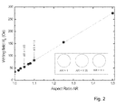
- FIG. 2 shows the dependence of the writing field H R of the storage layer, on the aspect ratio of the junction for a conventional TAS MTJ-based MRAM cell.
- AR 1.0 to 1.1
- the inset of figure 2 shows a top view of junctions with aspect ratio comprised between 1.0 and 1.1.
- An object of the invention is therefore to propose a new system and method which overcomes at least some limitations of the prior art.
- Another object of the invention is to provide a magnetic tunnel junction (MTJ) -based magnetic random access memory (MRAM) cell with a thermally assisted switching (TAS) writing procedure, having a reduced dependence of the dispersion of the writing field on the junction aspect ratio due to the fabrication process.
- MTJ magnetic tunnel junction
- MRAM magnetic random access memory
- TAS thermally assisted switching
- a TAS MTJ-based MRAM cell comprising a magnetic tunnel junction formed from a ferromagnetic storage layer having a magnetization that is adjustable above a high temperature threshold, a reference layer having a fixed magnetization, and an insulating layer being disposed between the storage and reference layers; said junction having an anisotropic shape, and said ferromagnetic storage layer having a magnetocrystalline anisotropy being oriented essentially perpendicular to the long axis of the anisotropic shape of the magnetic tunnel junction.
- the anisotropic shape of the magnetic tunnel junction is an elliptical or a rectangle or a crescent or a semi-ellipse or a diamond shape.
- the magnetic tunnel junction has an anisotropic shape with an aspect ratio comprised between 1.0 and 1.5.
- the magnetic tunnel junction has an anisotropic shape with an aspect ratio comprised between 1.0 and 1.1 or comprised between 1.0 and 1.05.
- the present invention also encompasses a method of writing data in the TAS MTJ-based MRAM cell, the cell further comprising a select transistor being coupled with the magnetic tunnel junction and controllable via a word line, a connecting current line electrically connected to the magnetic tunnel junction, and a word current line; the method comprising the steps of:
- ellipse generally refer to any closed shapes having an anisotropic form such as ellipses, crescents, semi-ellipses, diamonds, rectangles, etc.
- Advantages of the TAS MTJ-based MRAM cell of the present invention comprise limiting the effects of dispersion in the magnetic tunnel junction shape anisotropy coming from the fabrication process, a lower power consumption, and facilitated cell scaling down, compared with the MTJ-based MRAM and TAS MTJ-based MRAM cells of the prior art.
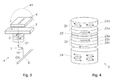
- FIG. 3 represents a thermally assisted switching (TAS) magnetic tunnel junction (MTJ) -based magnetic random access memory (MRAM) memory cell 1 according to an embodiment of the invention.
- the TAS MTJ-based MRAM cell 1 comprises a magnetic tunnel junction 2 placed between a selection CMOS select transistor 3 and a connecting current line 7 for passing a junction current pulse 31 flowing through the junction 2 when the transistor 3 is in the saturated or open mode (ON).
- a control current line 6 is used to control the opening and the closing of the transistor 3 in order to address each memory cell individually.
- the TAS MTJ-based MRAM cell 1 also comprises a word current line 4, shown above and perpendicular to the connecting current line 7 in the example of Fig. 3 .
- Other configurations of the word current line 4 are however possible.
- the word current line 4 can be placed parallel with the connecting current line 7 and/or on the side of or below the junction 2.
- the junction 2 contains a storage layer 21 preferably comprising a ferromagnetic storage layer 21 a and an antiferromagnetic storage layer 21 b.
- the ferromagnetic storage layer 21 a has a thickness typically of the order of 1 to 10 nm and is made of a material having a planar magnetization, typically selected from the group Permalloy (Ni 80 Fe 20 ), Co 90 Fe 10 or other alloys containing Fe, Co or Ni.
- the ferromagnetic storage layer 21 a is exchange-coupled by the antiferromagnetic storage layer 21 b made of a manganese-based alloy, for example, of IrMn or FeMn.
- the antiferromagnetic storage layer 21 b has a blocking temperature T BS sufficiently high to ensure that at a low temperature threshold below T BS , for example, at standby temperature, i.e., in the absence of heating, magnetization of the ferromagnetic storage layer 21 a is sufficiently pinned to be able to preserve its magnetization over a period of several years but not so high as to make it necessary to heat the junction excessively during every the writing process that could yield to material degradation and high power consumption.
- a T BS in the range of, for example, 120 to 220°C is suitable.
- the junction 2 also contains a reference layer 23 preferably comprising a first ferromagnetic reference layer 23a and a second ferromagnetic reference layer 23c, both formed of a Fe, Co or Ni based alloy.
- the two ferromagnetic reference layers 23a, 23c are antiferromagnetically coupled by inserting between them a non-ferromagnetic reference layer 23b made, for example, of ruthenium.
- the antiferromagnetic reference layer 24 orients the magnetic moment of the first ferromagnetic reference layer 23a, and a pinning field is generated that fixes the magnetic moment of the second ferromagnetic reference layer 23c.
- the reference layer structure described above is well known in the state of the art under the name of synthetic antiferromagnet pinned layer.
- Other configurations of the storage layer 23 are also possible.
- the reference layer 23 can comprise a single ferromagnetic reference layer pinned by the antiferromagnetic reference layer 24 described above.
- An insulating layer 22 playing the role of a tunnel barrier and preferably made of a material selected from the group comprising Al 2 O 3 and MgO is inserted between the storage layer 21 and the reference layer 23.
- the tunneling resistance of a junction depends exponentially on the insulating layer thickness and is measured by the resistance-area product (RA) of the junction.
- the RA must sufficiently small in order to flow the junction current 31 through the junction, sufficiently high to raise the temperature of the antiferromagnetic storage layer 21 b above its blocking temperature T BS .
- the RA value In order to force a current density in the range of 10 5 A/cm 2 to 10 7 A/cm 2 , typically required to raise the temperature of the junction up to 100°C, the RA value should be of the order of 1 to 500 ⁇ . ⁇ m 2 .
- the junction 2 at least one thermal barrier layer (not shown) made typically of BiTe or GeSbTe and having a very low thermal conductivity can be added at the top and at the bottom of the junction 2.
- the purpose of these additional layers is to increase the heating efficiency of the junction current 31 flowing through the junction while limiting the diffusion of the heat towards the electrode (not shown) ensuring the electrical connection between the junction 2 and the connecting current line 7.
- the thermal barrier itself is electrically connected to the electrode directly or via a conductive layer, for example made of TiN or TiWN.
- the junction current pulse 31 having a magnitude comprised between 10 5 A/cm 2 and 10 7 A/cm 2 and lasting several nanoseconds is sent through a connecting current line 7 and the junction 2 (with transistor ON), rising the temperature of the junction to a high temperature threshold of about 120 to 220°C, lying between T BS and T BR where the magnetic coupling between the ferromagnetic storage layer 21 a and antiferromagnetic storage layer 21 b disappears and the magnetization of the ferromagnetic storage layer 21 a, being no more pinned, can be freely adjusted.
- the junction 2 is then cooled while a moderate word magnetic field 41 is applied by flowing a current in the word current line 4, allowing for the aligning of the magnetization of the ferromagnetic storage layer 21 a in a direction according to the magnetic field 41 orientation, essentially parallel or antiparallel with the magnetization orientation of the reference layer 23.
- the magnetic tunnel junction 2 is then cooled down at a low temperature threshold below the blocking temperature T BS of the antiferromagnetic storage layer 21 b, where the magnetization of the ferromagnetic storage layer 21 a becomes pinned in its reversed direction, or written state.
- the magnetic tunnel junction 2 has an anisotropic shape, such as an elliptical shape, and the ferromagnetic storage layer 21 a has a magnetocrystalline anisotropy that is oriented essentially perpendicular to the long axis of the anisotropic shape of the junction 2.
- the magnetization of the ferromagnetic storage layer 21 a is oriented in a direction that is essentially perpendicular with the long axis, or easy axis, of the anisotropic shape of the junction 2 at a high temperature threshold, when the magnetization of the ferromagnetic storage layer 21 a can be freely adjusted.
- FIG. 5 compares the variation of the word magnetic field 41, or writing field H R , with the junction aspect ratio AR for a conventional memory cell, where the ferromagnetic storage layer 21 a has a magnetocrystalline anisotropy axis parallel to the long axis of the ellipse (filled circles), and for the memory cell 1 of the invention, where the ferromagnetic storage layer 21 a has a magnetocrystalline anisotropy axis perpendicular to the long axis of the ellipse (open circles).
- the variation of the writing field H R has been calculated for the junction anisotropic shapes having aspect ratios AR comprised between 1.0 and 1.1.
- the calculations were performed by means of micromagnetic simulations assuming standard material parameters corresponding to the ferromagnetic storage layer 21 a employed in a usual TAS MTJ-based MRAM cell 1 and assuming that the writing field H R is applied parallel to the magnetocrystalline anisotropy axis.
- the shape of the junction 2 is not limited to an elliptical shape but can have any shape that is anisotropic, such as a rectangle, crescent, semi-ellipse, diamond, etc., where the magnetocrystalline anisotropy axis is essentially perpendicular to the long axis of the anisotropic shape of the junction 2.
- the writing field H R increases approximately linearly with the memory cell aspect ratio AR, for a magnetocrystalline anisotropy axis of the ferromagnetic storage layer 21a that is essentially parallel to the long axis of the ellipse.
- a variation in the memory cell aspect ratio AR due to the manufacturing process will result in an overall increase in the writing field H R and a larger power consumption of the magnetic memory device.
- the writing field H R decreases approximately linearly with the aspect ratio AR, and a variation in the memory cell aspect ratio AR will tend to diminish the overall writing field H R and power consumption of the magnetic memory cell 1.
- the junction 2 of the memory cell is characterized by an aspect ratio AR equal or above a value of 1.0, corresponding to a circular (or square, etc.) junction 2, but preferably comprised between 1.0 and 1.5, and a magnetocrystalline anisotropy axis of the ferromagnetic storage layer 21 a perpendicular to the long axis of the ellipse.
- a magnetic memory device (not represented) can be formed by assembling a matrix comprising a plurality of TAS MTJ-based MRAM cells 1 of the invention, where each junction 2 of each memory cell 1 is connected on the side of the storage layer 21, or ferromagnetic storage layer 21 a, to the connecting current line 7, and on the opposite side to the control current line 6, placed perpendicular with the connecting current line 7.
- a current pulse is sent in one or several control lines 6 in order to put at least one of the transistors 3 of the corresponding control lines 6 in mode ON, and a junction current pulse 31 is sent to each connecting lines 7 corresponding to the memory cells 1 to be written, i.e., the memory cells 1 placed at the intersection of the active connecting current lines 7 and active control lines 6.
- ⁇ e in the shape anisotropy of the junction 2 of about ⁇ 5% can be typically obtained.
- an anisotropic shape with an aspect ratio AR of 1.05 corresponds to a writing field H R of about 25 Oe, for the TAS MTJ-based MRAM cell 1 of the invention. This represents a decrease of about 30% in the writing field value compared to the one calculated for a junction 2 with an aspect ratio AR of 1.
- the junction 2 of the memory cell 1 has an aspect ratio AR comprised within the maximum shape anisotropy variations allowed by the fabrication process used for the memory cell fabrication, and has a magnetocrystalline anisotropy axis of the ferromagnetic storage layer 21 a perpendicular to the long axis of the junction anisotropic shape.
- the junction 2 of the memory cell 1 has an aspect ratio AR comprised between 1.0 and 1.1.
- the junction 2 of the memory cell 1 could be characterized by an aspect ratio AR comprised between 1.0 and 1.05, or even smaller.
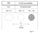
- Fig. 6 compares schematically the top view of a conventional junction with a field induced magnetic switching (FIMS) architecture having an aspect ratio AR of 1.5, with two junctions 2 of the TAS MTJ-based MRAM cell 1 of the present invention having aspect ratios AR of 1.0 and 1.05 respectively.
- FIMS field induced magnetic switching
- the variation of the junction aspect ratio AR is minimized by using an appropriate fabrication process and/or by a careful control of the fabrication process and/or by selecting fabricated memory cells 1 having the least variation possible in their aspect ratio AR.
- the magnetic memory device containing such junctions 2 with an aspect ratio AR of about 1.0 or any other value can be fabricated with no or a very small dispersion in the aspect ratio AR.
- Such memory device can have minimal variations of the writing field H R due to the combined effect of the small or inexistent dispersion, in the junction aspect ratios AR, and in the magnetocrystalline anisotropy axis of the ferromagnetic storage layer 21 a being essentially perpendicular to the long axis of the anisotropic shape of the junctions 2.
- the junctions 2 of the memory device have a magnetocrystalline anisotropy axis of the ferromagnetic storage layer 21 a essentially parallel to the long axis of the junction anisotropic shape, the latter having a very small or no dispersion of the aspect ratio AR.
- the magnetocrystalline anisotropy axis of the ferromagnetic storage layer 21 a is perpendicular to the long axis of the anisotropic shape of the junction 2, gives rise to a competition between the magnetocrystalline anisotropy and shape anisotropy terms of the barrier energy, E b .
- the magnetic moments of the ferromagnetic storage layer 21 a may be tilted with respect to the magnetic moments of the reference layer 23. This tilt can increase with increasing aspect ratios AR, translating in an important dispersion in the resistance value during the reading operation, and resulting in a loss in the read margin that corresponds to the difference between low and high resistance states.
- the writing sequence comprises a last cooling step of the junction 2, performed under the word magnetic field 41, corresponding to the writing field H R .
- This word magnetic field 41 "freezes" the magnetic state of the ferromagnetic storage layer 21 a resulting in a much reduced tilt of the magnetic moments of the ferromagnetic storage layer 21a with respect to the reference layer 23, yielding to a much lesser influence in the read margin. For example, a loss of less than 20% for the read margin is expected in the case of the junction 2 with a shape anisotropy variation of 10%.
- the junction 2 is fabricated with an isotropic (circular, square, etc.) or anisotropic (elliptical, rectangular, etc.) geometry and has a magnetocrystalline anisotropy axis of the ferromagnetic storage layer 21 a, essentially parallel to the long axis of the anisotropic shape of the junction 2.
- An example of another TAS MTJ-based MRAM cell 1 configuration is the memory cell described in unpublished patent application EP07291520 by the present applicant, where the junction 2 comprises a writing layer added on top of the storage layer 21.
- Another example is the junction described in patent application US2005002228 of a general thermally assisted MRAM architecture, where the writing process is ensured by the combination of one magnetic field and a local heating, and the storage layer is exchanged biased with an antiferromagnetic layer.
Landscapes
- Engineering & Computer Science (AREA)
- Computer Hardware Design (AREA)
- Mram Or Spin Memory Techniques (AREA)
- Hall/Mr Elements (AREA)
Priority Applications (1)
| Application Number | Priority Date | Filing Date | Title |
|---|---|---|---|
| EP09160167.4A EP2124228B1 (de) | 2008-05-20 | 2009-05-13 | Magnetischer Direktzugriffsspeicher mit einem elliptischen Tunnelübergang |
Applications Claiming Priority (2)
| Application Number | Priority Date | Filing Date | Title |
|---|---|---|---|
| EP08290468 | 2008-05-20 | ||
| EP09160167.4A EP2124228B1 (de) | 2008-05-20 | 2009-05-13 | Magnetischer Direktzugriffsspeicher mit einem elliptischen Tunnelübergang |
Publications (2)
| Publication Number | Publication Date |
|---|---|
| EP2124228A1 true EP2124228A1 (de) | 2009-11-25 |
| EP2124228B1 EP2124228B1 (de) | 2014-03-05 |
Family
ID=40943713
Family Applications (1)
| Application Number | Title | Priority Date | Filing Date |
|---|---|---|---|
| EP09160167.4A Active EP2124228B1 (de) | 2008-05-20 | 2009-05-13 | Magnetischer Direktzugriffsspeicher mit einem elliptischen Tunnelübergang |
Country Status (3)
| Country | Link |
|---|---|
| US (1) | US8064245B2 (de) |
| EP (1) | EP2124228B1 (de) |
| JP (1) | JP5513008B2 (de) |
Families Citing this family (14)
| Publication number | Priority date | Publication date | Assignee | Title |
|---|---|---|---|---|
| US8194436B2 (en) * | 2007-09-19 | 2012-06-05 | Nec Corporation | Magnetic random access memory, write method therefor, and magnetoresistance effect element |
| US8400066B1 (en) | 2010-08-01 | 2013-03-19 | Lawrence T. Pileggi | Magnetic logic circuits and systems incorporating same |
| EP2447948B1 (de) * | 2010-10-26 | 2014-12-31 | Crocus Technology S.A. | Thermisch gestütztes magnetisches Direktzugriffspeicherelement mit verbesserter Dauerhaftigkeit |
| US8472240B2 (en) | 2011-05-16 | 2013-06-25 | Micron Technology, Inc. | Spin torque transfer memory cell structures and methods |
| EP2608208B1 (de) * | 2011-12-22 | 2015-02-11 | Crocus Technology S.A. | Selbstbezogene MRAM-Zelle und Verfahren zum Beschreiben der Zelle unter Verwendung eines SST-Vorgangs |
| US8923041B2 (en) * | 2012-04-11 | 2014-12-30 | Everspin Technologies, Inc. | Self-referenced sense amplifier for spin torque MRAM |
| US20140124880A1 (en) | 2012-11-06 | 2014-05-08 | International Business Machines Corporation | Magnetoresistive random access memory |
| US8750033B2 (en) | 2012-11-06 | 2014-06-10 | International Business Machines Corporation | Reading a cross point cell array |
| US9070868B2 (en) | 2013-06-04 | 2015-06-30 | International Business Machines Corporation | Thermally assisted MRAM with a multilayer encapsulant for low thermal conductivity |
| FR3031622B1 (fr) * | 2015-01-14 | 2018-02-16 | Centre National De La Recherche Scientifique | Point memoire magnetique |
| US10177197B2 (en) | 2015-11-16 | 2019-01-08 | Samsung Electronics Co., Ltd. | Magnetic junctions having elongated free layers |
| US10332576B2 (en) * | 2017-06-07 | 2019-06-25 | International Business Machines Corporation | Magnetic exchange coupled MTJ free layer with double tunnel barriers having low switching current and high data retention |
| US10510390B2 (en) * | 2017-06-07 | 2019-12-17 | International Business Machines Corporation | Magnetic exchange coupled MTJ free layer having low switching current and high data retention |
| CN112563411B (zh) * | 2020-11-19 | 2023-08-08 | 中国科学院微电子研究所 | 一种磁性隧道结及其制造方法、存储单元 |
Citations (10)
| Publication number | Priority date | Publication date | Assignee | Title |
|---|---|---|---|---|
| US4949039A (en) | 1988-06-16 | 1990-08-14 | Kernforschungsanlage Julich Gmbh | Magnetic field sensor with ferromagnetic thin layers having magnetically antiparallel polarized components |
| US5159513A (en) | 1991-02-08 | 1992-10-27 | International Business Machines Corporation | Magnetoresistive sensor based on the spin valve effect |
| US5343422A (en) | 1993-02-23 | 1994-08-30 | International Business Machines Corporation | Nonvolatile magnetoresistive storage device using spin valve effect |
| US5583725A (en) | 1994-06-15 | 1996-12-10 | International Business Machines Corporation | Spin valve magnetoresistive sensor with self-pinned laminated layer and magnetic recording system using the sensor |
| US5640343A (en) | 1996-03-18 | 1997-06-17 | International Business Machines Corporation | Magnetic memory array using magnetic tunnel junction devices in the memory cells |
| US5959880A (en) | 1997-12-18 | 1999-09-28 | Motorola, Inc. | Low aspect ratio magnetoresistive tunneling junction |
| US20050002228A1 (en) | 2001-11-16 | 2005-01-06 | Bernard Dieny | Magnetic device with magnetic tunnel junction, memory array and read/write methods using same |
| US6954375B2 (en) * | 2002-11-15 | 2005-10-11 | Sony Corporation | Magnetic storage element, recording method using the same, and magnetic storage device |
| US20060291276A1 (en) | 2004-02-23 | 2006-12-28 | Centre National De La Recherche Scientifique - Cnrs | Magnetic memory with a magnetic tunnel junction written in a thermally assisted manner, and method for writing the same |
| WO2008040561A2 (en) * | 2006-10-06 | 2008-04-10 | Crocus Technology S.A. | System and method for providing content-addressable magnetoresistive random access memory cells |
Family Cites Families (35)
| Publication number | Priority date | Publication date | Assignee | Title |
|---|---|---|---|---|
| JP4078696B2 (ja) | 1997-11-28 | 2008-04-23 | 松下電器産業株式会社 | 記録許可判定装置及び情報記録装置 |
| US6317349B1 (en) | 1999-04-16 | 2001-11-13 | Sandisk Corporation | Non-volatile content addressable memory |
| US6535416B1 (en) | 1999-06-18 | 2003-03-18 | Nve Corporation | Magnetic memory coincident thermal pulse data storage |
| JP5254514B2 (ja) * | 1999-09-10 | 2013-08-07 | コーニンクレッカ フィリップス エレクトロニクス エヌ ヴィ | 減少した電磁切換え磁場を持つ磁気抵抗検知器又は記憶素子 |
| US6191973B1 (en) | 1999-09-27 | 2001-02-20 | Motorola Inc. | Mram cam |
| RU2268258C2 (ru) * | 2000-03-16 | 2006-01-20 | Ф.Хоффманн-Ля Рош Аг | Производные карбоновых кислот в качестве антагонистов ip |
| US6269016B1 (en) | 2000-06-19 | 2001-07-31 | Motorola Inc. | MRAM cam |
| US6724674B2 (en) | 2000-11-08 | 2004-04-20 | International Business Machines Corporation | Memory storage device with heating element |
| US6385082B1 (en) | 2000-11-08 | 2002-05-07 | International Business Machines Corp. | Thermally-assisted magnetic random access memory (MRAM) |
| JP4726292B2 (ja) | 2000-11-14 | 2011-07-20 | ルネサスエレクトロニクス株式会社 | 薄膜磁性体記憶装置 |
| FR2817999B1 (fr) | 2000-12-07 | 2003-01-10 | Commissariat Energie Atomique | Dispositif magnetique a polarisation de spin et a empilement(s) tri-couche(s) et memoire utilisant ce dispositif |
| FR2817998B1 (fr) | 2000-12-07 | 2003-01-10 | Commissariat Energie Atomique | Dispositif magnetique a polarisation de spin et a rotation d'aimantation, memoire et procede d'ecriture utilisant ce dispositif |
| JP3920564B2 (ja) | 2000-12-25 | 2007-05-30 | 株式会社東芝 | 磁気ランダムアクセスメモリ |
| US6304477B1 (en) | 2001-01-31 | 2001-10-16 | Motorola, Inc. | Content addressable magnetic random access memory |
| US6760249B2 (en) | 2001-06-21 | 2004-07-06 | Pien Chien | Content addressable memory device capable of comparing data bit with storage data bit |
| JP4798895B2 (ja) * | 2001-08-21 | 2011-10-19 | キヤノン株式会社 | 強磁性体メモリとその熱補助駆動方法 |
| FR2829867B1 (fr) | 2001-09-20 | 2003-12-19 | Centre Nat Rech Scient | Memoire magnetique a selection a l'ecriture par inhibition et procede pour son ecriture |
| FR2829868A1 (fr) | 2001-09-20 | 2003-03-21 | Centre Nat Rech Scient | Memoire magnetique a ecriture par courant polarise en spin, mettant en oeuvre des alliages amorphes ferrimagnetiques et procede pour son ecriture |
| JP4084036B2 (ja) * | 2001-12-04 | 2008-04-30 | 株式会社リコー | 磁気センサ及びこの磁気センサを用いた方位検知システム |
| US6750491B2 (en) | 2001-12-20 | 2004-06-15 | Hewlett-Packard Development Company, L.P. | Magnetic memory device having soft reference layer |
| US6771534B2 (en) * | 2002-11-15 | 2004-08-03 | International Business Machines Corporation | Thermally-assisted magnetic writing using an oxide layer and current-induced heating |
| US7173846B2 (en) | 2003-02-13 | 2007-02-06 | Taiwan Semiconductor Manufacturing Company, Ltd. | Magnetic RAM and array architecture using a two transistor, one MTJ cell |
| WO2005001490A2 (en) | 2003-06-23 | 2005-01-06 | Nve Corporation | Thermally operated switch control memory cell |
| JP2005064050A (ja) | 2003-08-14 | 2005-03-10 | Toshiba Corp | 半導体記憶装置及びそのデータ書き込み方法 |
| KR100568512B1 (ko) * | 2003-09-29 | 2006-04-07 | 삼성전자주식회사 | 열발생층을 갖는 자기열 램셀들 및 이를 구동시키는 방법들 |
| US7372722B2 (en) * | 2003-09-29 | 2008-05-13 | Samsung Electronics Co., Ltd. | Methods of operating magnetic random access memory devices including heat-generating structures |
| FR2860910B1 (fr) | 2003-10-10 | 2006-02-10 | Commissariat Energie Atomique | Dispositif a jonction tunnel magnetique et procede d'ecriture/lecture d'un tel dispositif |
| WO2005036558A1 (en) | 2003-10-14 | 2005-04-21 | Agency For Science, Technology And Research | Magnetic memory device |
| US7012832B1 (en) | 2003-10-31 | 2006-03-14 | Western Digital (Fremont), Inc. | Magnetic memory cell with plural read transistors |
| FR2867300B1 (fr) | 2004-03-05 | 2006-04-28 | Commissariat Energie Atomique | Memoire vive magnetoresistive a haute densite de courant |
| US7154798B2 (en) * | 2004-04-27 | 2006-12-26 | Taiwan Semiconductor Manufacturing Company, Ltd. | MRAM arrays and methods for writing and reading magnetic memory devices |
| KR100642638B1 (ko) * | 2004-10-21 | 2006-11-10 | 삼성전자주식회사 | 낮은 임계 전류를 갖는 자기 램 소자의 구동 방법들 |
| KR100612878B1 (ko) * | 2004-12-03 | 2006-08-14 | 삼성전자주식회사 | 자기 메모리 소자와 그 제조 및 동작방법 |
| US7532505B1 (en) | 2006-07-17 | 2009-05-12 | Grandis, Inc. | Method and system for using a pulsed field to assist spin transfer induced switching of magnetic memory elements |
| EP2109111B1 (de) | 2008-04-07 | 2011-12-21 | Crocus Technology S.A. | System und Verfahren zum Schreiben von Daten auf magnetoresistive Direktzugriffsspeicherzellen |
-
2009
- 2009-05-13 EP EP09160167.4A patent/EP2124228B1/de active Active
- 2009-05-15 US US12/467,171 patent/US8064245B2/en active Active
- 2009-05-19 JP JP2009120741A patent/JP5513008B2/ja not_active Expired - Fee Related
Patent Citations (11)
| Publication number | Priority date | Publication date | Assignee | Title |
|---|---|---|---|---|
| US4949039A (en) | 1988-06-16 | 1990-08-14 | Kernforschungsanlage Julich Gmbh | Magnetic field sensor with ferromagnetic thin layers having magnetically antiparallel polarized components |
| US5159513A (en) | 1991-02-08 | 1992-10-27 | International Business Machines Corporation | Magnetoresistive sensor based on the spin valve effect |
| US5343422A (en) | 1993-02-23 | 1994-08-30 | International Business Machines Corporation | Nonvolatile magnetoresistive storage device using spin valve effect |
| US5583725A (en) | 1994-06-15 | 1996-12-10 | International Business Machines Corporation | Spin valve magnetoresistive sensor with self-pinned laminated layer and magnetic recording system using the sensor |
| US5640343A (en) | 1996-03-18 | 1997-06-17 | International Business Machines Corporation | Magnetic memory array using magnetic tunnel junction devices in the memory cells |
| US5959880A (en) | 1997-12-18 | 1999-09-28 | Motorola, Inc. | Low aspect ratio magnetoresistive tunneling junction |
| US20050002228A1 (en) | 2001-11-16 | 2005-01-06 | Bernard Dieny | Magnetic device with magnetic tunnel junction, memory array and read/write methods using same |
| US6954375B2 (en) * | 2002-11-15 | 2005-10-11 | Sony Corporation | Magnetic storage element, recording method using the same, and magnetic storage device |
| US20060291276A1 (en) | 2004-02-23 | 2006-12-28 | Centre National De La Recherche Scientifique - Cnrs | Magnetic memory with a magnetic tunnel junction written in a thermally assisted manner, and method for writing the same |
| WO2008040561A2 (en) * | 2006-10-06 | 2008-04-10 | Crocus Technology S.A. | System and method for providing content-addressable magnetoresistive random access memory cells |
| US7518897B2 (en) * | 2006-10-06 | 2009-04-14 | Crocus Technology S.A. | System and method for providing content-addressable magnetoresistive random access memory cells |
Non-Patent Citations (2)
| Title |
|---|
| PURNAMA ET AL: "Micromagnetic simulation of thermally assisted magnetization reversal in magnetic nanodots with perpendicular anisotropy", JOURNAL OF MAGNETISM AND MAGNETIC MATERIALS, ELSEVIER SCIENCE PUBLISHERS, AMSTERDAM, NL, vol. 310, no. 2, 16 March 2007 (2007-03-16), pages 2683 - 2685, XP022048680, ISSN: 0304-8853 * |
| PURNAMA: "Journal of Magnetism and Magnetic Materials", vol. 310, 16 March 2007, ELSEVIER SCIENCE PUBLISHERS, article "Micromagnetic simulation of thermally assisted magnetization reversal in magnetic nanodots with perpendicular anisotropy", pages: 2683 - 2685 |
Also Published As
| Publication number | Publication date |
|---|---|
| JP2009283938A (ja) | 2009-12-03 |
| JP5513008B2 (ja) | 2014-06-04 |
| EP2124228B1 (de) | 2014-03-05 |
| US20090290413A1 (en) | 2009-11-26 |
| US8064245B2 (en) | 2011-11-22 |
Similar Documents
| Publication | Publication Date | Title |
|---|---|---|
| EP2124228B1 (de) | Magnetischer Direktzugriffsspeicher mit einem elliptischen Tunnelübergang | |
| EP2232495B1 (de) | Magnetspeicher mit einem wärmeunterstützten schreibverfahren | |
| US7796428B2 (en) | Thermally assisted magnetic write memory | |
| US8385107B2 (en) | Magnetic memory with a thermally assisted spin transfer torque writing procedure using a low writing current | |
| JP5441881B2 (ja) | 磁気トンネル接合を備えた磁気メモリ | |
| US8711608B2 (en) | Memory with separate read and write paths | |
| EP2477227B1 (de) | Magnettunnelübergang mit einer Polarisierungsschicht | |
| US7859892B2 (en) | Magnetic random access memory with dual spin torque reference layers | |
| US20170179372A1 (en) | Spin-orbit torque bit design for improved switching efficiency | |
| US8391053B2 (en) | Magnetic memory with a thermally assisted writing procedure and reduced writing field | |
| JP2011507243A5 (de) | ||
| EP2608208A1 (de) | Selbstbezogene MRAM-Zelle und Verfahren zum Beschreiben der Zelle unter Verwendung eines SST-Vorgangs | |
| US8503225B2 (en) | Multibit cell with synthetic storage layer | |
| US7466585B2 (en) | Magnetic random access memory |
Legal Events
| Date | Code | Title | Description |
|---|---|---|---|
| PUAI | Public reference made under article 153(3) epc to a published international application that has entered the european phase |
Free format text: ORIGINAL CODE: 0009012 |
|
| AK | Designated contracting states |
Kind code of ref document: A1 Designated state(s): AT BE BG CH CY CZ DE DK EE ES FI FR GB GR HR HU IE IS IT LI LT LU LV MC MK MT NL NO PL PT RO SE SI SK TR |
|
| 17P | Request for examination filed |
Effective date: 20100331 |
|
| 17Q | First examination report despatched |
Effective date: 20101119 |
|
| GRAP | Despatch of communication of intention to grant a patent |
Free format text: ORIGINAL CODE: EPIDOSNIGR1 |
|
| INTG | Intention to grant announced |
Effective date: 20131018 |
|
| GRAS | Grant fee paid |
Free format text: ORIGINAL CODE: EPIDOSNIGR3 |
|
| GRAA | (expected) grant |
Free format text: ORIGINAL CODE: 0009210 |
|
| AK | Designated contracting states |
Kind code of ref document: B1 Designated state(s): AT BE BG CH CY CZ DE DK EE ES FI FR GB GR HR HU IE IS IT LI LT LU LV MC MK MT NL NO PL PT RO SE SI SK TR |
|
| REG | Reference to a national code |
Ref country code: GB Ref legal event code: FG4D |
|
| REG | Reference to a national code |
Ref country code: CH Ref legal event code: EP |
|
| REG | Reference to a national code |
Ref country code: AT Ref legal event code: REF Ref document number: 655354 Country of ref document: AT Kind code of ref document: T Effective date: 20140315 |
|
| REG | Reference to a national code |
Ref country code: IE Ref legal event code: FG4D |
|
| REG | Reference to a national code |
Ref country code: DE Ref legal event code: R096 Ref document number: 602009022129 Country of ref document: DE Effective date: 20140417 |
|
| REG | Reference to a national code |
Ref country code: NL Ref legal event code: T3 |
|
| REG | Reference to a national code |
Ref country code: AT Ref legal event code: MK05 Ref document number: 655354 Country of ref document: AT Kind code of ref document: T Effective date: 20140305 |
|
| PG25 | Lapsed in a contracting state [announced via postgrant information from national office to epo] |
Ref country code: NO Free format text: LAPSE BECAUSE OF FAILURE TO SUBMIT A TRANSLATION OF THE DESCRIPTION OR TO PAY THE FEE WITHIN THE PRESCRIBED TIME-LIMIT Effective date: 20140605 Ref country code: LT Free format text: LAPSE BECAUSE OF FAILURE TO SUBMIT A TRANSLATION OF THE DESCRIPTION OR TO PAY THE FEE WITHIN THE PRESCRIBED TIME-LIMIT Effective date: 20140305 |
|
| REG | Reference to a national code |
Ref country code: LT Ref legal event code: MG4D |
|
| PG25 | Lapsed in a contracting state [announced via postgrant information from national office to epo] |
Ref country code: AT Free format text: LAPSE BECAUSE OF FAILURE TO SUBMIT A TRANSLATION OF THE DESCRIPTION OR TO PAY THE FEE WITHIN THE PRESCRIBED TIME-LIMIT Effective date: 20140305 Ref country code: CY Free format text: LAPSE BECAUSE OF FAILURE TO SUBMIT A TRANSLATION OF THE DESCRIPTION OR TO PAY THE FEE WITHIN THE PRESCRIBED TIME-LIMIT Effective date: 20140305 Ref country code: FI Free format text: LAPSE BECAUSE OF FAILURE TO SUBMIT A TRANSLATION OF THE DESCRIPTION OR TO PAY THE FEE WITHIN THE PRESCRIBED TIME-LIMIT Effective date: 20140305 Ref country code: SE Free format text: LAPSE BECAUSE OF FAILURE TO SUBMIT A TRANSLATION OF THE DESCRIPTION OR TO PAY THE FEE WITHIN THE PRESCRIBED TIME-LIMIT Effective date: 20140305 |
|
| PG25 | Lapsed in a contracting state [announced via postgrant information from national office to epo] |
Ref country code: LV Free format text: LAPSE BECAUSE OF FAILURE TO SUBMIT A TRANSLATION OF THE DESCRIPTION OR TO PAY THE FEE WITHIN THE PRESCRIBED TIME-LIMIT Effective date: 20140305 Ref country code: HR Free format text: LAPSE BECAUSE OF FAILURE TO SUBMIT A TRANSLATION OF THE DESCRIPTION OR TO PAY THE FEE WITHIN THE PRESCRIBED TIME-LIMIT Effective date: 20140305 |
|
| PG25 | Lapsed in a contracting state [announced via postgrant information from national office to epo] |
Ref country code: EE Free format text: LAPSE BECAUSE OF FAILURE TO SUBMIT A TRANSLATION OF THE DESCRIPTION OR TO PAY THE FEE WITHIN THE PRESCRIBED TIME-LIMIT Effective date: 20140305 Ref country code: RO Free format text: LAPSE BECAUSE OF FAILURE TO SUBMIT A TRANSLATION OF THE DESCRIPTION OR TO PAY THE FEE WITHIN THE PRESCRIBED TIME-LIMIT Effective date: 20140305 Ref country code: CZ Free format text: LAPSE BECAUSE OF FAILURE TO SUBMIT A TRANSLATION OF THE DESCRIPTION OR TO PAY THE FEE WITHIN THE PRESCRIBED TIME-LIMIT Effective date: 20140305 Ref country code: BG Free format text: LAPSE BECAUSE OF FAILURE TO SUBMIT A TRANSLATION OF THE DESCRIPTION OR TO PAY THE FEE WITHIN THE PRESCRIBED TIME-LIMIT Effective date: 20140605 Ref country code: IS Free format text: LAPSE BECAUSE OF FAILURE TO SUBMIT A TRANSLATION OF THE DESCRIPTION OR TO PAY THE FEE WITHIN THE PRESCRIBED TIME-LIMIT Effective date: 20140705 Ref country code: BE Free format text: LAPSE BECAUSE OF FAILURE TO SUBMIT A TRANSLATION OF THE DESCRIPTION OR TO PAY THE FEE WITHIN THE PRESCRIBED TIME-LIMIT Effective date: 20140305 |
|
| PG25 | Lapsed in a contracting state [announced via postgrant information from national office to epo] |
Ref country code: SK Free format text: LAPSE BECAUSE OF FAILURE TO SUBMIT A TRANSLATION OF THE DESCRIPTION OR TO PAY THE FEE WITHIN THE PRESCRIBED TIME-LIMIT Effective date: 20140305 Ref country code: PL Free format text: LAPSE BECAUSE OF FAILURE TO SUBMIT A TRANSLATION OF THE DESCRIPTION OR TO PAY THE FEE WITHIN THE PRESCRIBED TIME-LIMIT Effective date: 20140305 Ref country code: ES Free format text: LAPSE BECAUSE OF FAILURE TO SUBMIT A TRANSLATION OF THE DESCRIPTION OR TO PAY THE FEE WITHIN THE PRESCRIBED TIME-LIMIT Effective date: 20140305 |
|
| REG | Reference to a national code |
Ref country code: DE Ref legal event code: R097 Ref document number: 602009022129 Country of ref document: DE |
|
| PG25 | Lapsed in a contracting state [announced via postgrant information from national office to epo] |
Ref country code: LU Free format text: LAPSE BECAUSE OF FAILURE TO SUBMIT A TRANSLATION OF THE DESCRIPTION OR TO PAY THE FEE WITHIN THE PRESCRIBED TIME-LIMIT Effective date: 20140513 Ref country code: PT Free format text: LAPSE BECAUSE OF FAILURE TO SUBMIT A TRANSLATION OF THE DESCRIPTION OR TO PAY THE FEE WITHIN THE PRESCRIBED TIME-LIMIT Effective date: 20140707 |
|
| REG | Reference to a national code |
Ref country code: CH Ref legal event code: PL |
|
| PLBE | No opposition filed within time limit |
Free format text: ORIGINAL CODE: 0009261 |
|
| STAA | Information on the status of an ep patent application or granted ep patent |
Free format text: STATUS: NO OPPOSITION FILED WITHIN TIME LIMIT |
|
| PG25 | Lapsed in a contracting state [announced via postgrant information from national office to epo] |
Ref country code: MC Free format text: LAPSE BECAUSE OF FAILURE TO SUBMIT A TRANSLATION OF THE DESCRIPTION OR TO PAY THE FEE WITHIN THE PRESCRIBED TIME-LIMIT Effective date: 20140305 Ref country code: LI Free format text: LAPSE BECAUSE OF NON-PAYMENT OF DUE FEES Effective date: 20140531 Ref country code: DK Free format text: LAPSE BECAUSE OF FAILURE TO SUBMIT A TRANSLATION OF THE DESCRIPTION OR TO PAY THE FEE WITHIN THE PRESCRIBED TIME-LIMIT Effective date: 20140305 Ref country code: CH Free format text: LAPSE BECAUSE OF NON-PAYMENT OF DUE FEES Effective date: 20140531 |
|
| 26N | No opposition filed |
Effective date: 20141208 |
|
| REG | Reference to a national code |
Ref country code: IE Ref legal event code: MM4A |
|
| REG | Reference to a national code |
Ref country code: DE Ref legal event code: R097 Ref document number: 602009022129 Country of ref document: DE Effective date: 20141208 |
|
| PG25 | Lapsed in a contracting state [announced via postgrant information from national office to epo] |
Ref country code: IT Free format text: LAPSE BECAUSE OF FAILURE TO SUBMIT A TRANSLATION OF THE DESCRIPTION OR TO PAY THE FEE WITHIN THE PRESCRIBED TIME-LIMIT Effective date: 20140305 |
|
| PG25 | Lapsed in a contracting state [announced via postgrant information from national office to epo] |
Ref country code: IE Free format text: LAPSE BECAUSE OF NON-PAYMENT OF DUE FEES Effective date: 20140513 |
|
| REG | Reference to a national code |
Ref country code: FR Ref legal event code: PLFP Year of fee payment: 7 |
|
| PG25 | Lapsed in a contracting state [announced via postgrant information from national office to epo] |
Ref country code: SI Free format text: LAPSE BECAUSE OF FAILURE TO SUBMIT A TRANSLATION OF THE DESCRIPTION OR TO PAY THE FEE WITHIN THE PRESCRIBED TIME-LIMIT Effective date: 20140305 |
|
| REG | Reference to a national code |
Ref country code: FR Ref legal event code: GC Effective date: 20151118 |
|
| PG25 | Lapsed in a contracting state [announced via postgrant information from national office to epo] |
Ref country code: MT Free format text: LAPSE BECAUSE OF FAILURE TO SUBMIT A TRANSLATION OF THE DESCRIPTION OR TO PAY THE FEE WITHIN THE PRESCRIBED TIME-LIMIT Effective date: 20140305 |
|
| REG | Reference to a national code |
Ref country code: FR Ref legal event code: PLFP Year of fee payment: 8 |
|
| PG25 | Lapsed in a contracting state [announced via postgrant information from national office to epo] |
Ref country code: GR Free format text: LAPSE BECAUSE OF FAILURE TO SUBMIT A TRANSLATION OF THE DESCRIPTION OR TO PAY THE FEE WITHIN THE PRESCRIBED TIME-LIMIT Effective date: 20140606 |
|
| PGFP | Annual fee paid to national office [announced via postgrant information from national office to epo] |
Ref country code: NL Payment date: 20160519 Year of fee payment: 8 |
|
| PG25 | Lapsed in a contracting state [announced via postgrant information from national office to epo] |
Ref country code: TR Free format text: LAPSE BECAUSE OF FAILURE TO SUBMIT A TRANSLATION OF THE DESCRIPTION OR TO PAY THE FEE WITHIN THE PRESCRIBED TIME-LIMIT Effective date: 20140305 Ref country code: HU Free format text: LAPSE BECAUSE OF FAILURE TO SUBMIT A TRANSLATION OF THE DESCRIPTION OR TO PAY THE FEE WITHIN THE PRESCRIBED TIME-LIMIT; INVALID AB INITIO Effective date: 20090513 |
|
| REG | Reference to a national code |
Ref country code: FR Ref legal event code: PLFP Year of fee payment: 9 |
|
| REG | Reference to a national code |
Ref country code: NL Ref legal event code: MM Effective date: 20170601 |
|
| PG25 | Lapsed in a contracting state [announced via postgrant information from national office to epo] |
Ref country code: NL Free format text: LAPSE BECAUSE OF NON-PAYMENT OF DUE FEES Effective date: 20170601 |
|
| REG | Reference to a national code |
Ref country code: FR Ref legal event code: PLFP Year of fee payment: 10 |
|
| PG25 | Lapsed in a contracting state [announced via postgrant information from national office to epo] |
Ref country code: MK Free format text: LAPSE BECAUSE OF FAILURE TO SUBMIT A TRANSLATION OF THE DESCRIPTION OR TO PAY THE FEE WITHIN THE PRESCRIBED TIME-LIMIT Effective date: 20140305 |
|
| REG | Reference to a national code |
Ref country code: DE Ref legal event code: R082 Ref document number: 602009022129 Country of ref document: DE Representative=s name: BECK & ROESSIG EUROPEAN PATENT ATTORNEYS, DE Ref country code: DE Ref legal event code: R082 Ref document number: 602009022129 Country of ref document: DE Representative=s name: BECK & ROESSIG - EUROPEAN PATENT ATTORNEYS, DE |
|
| P01 | Opt-out of the competence of the unified patent court (upc) registered |
Effective date: 20230620 |
|
| PGFP | Annual fee paid to national office [announced via postgrant information from national office to epo] |
Ref country code: FR Payment date: 20230525 Year of fee payment: 15 Ref country code: DE Payment date: 20230519 Year of fee payment: 15 |
|
| REG | Reference to a national code |
Ref country code: DE Ref legal event code: R081 Ref document number: 602009022129 Country of ref document: DE Owner name: CROCUS TECHNOLOGY SA, FR Free format text: FORMER OWNER: CROCUS TECHNOLOGY, GRENOBLE, FR Ref country code: DE Ref legal event code: R081 Ref document number: 602009022129 Country of ref document: DE Owner name: ALLEGRO MICRO SYSTEMS LLC, MANCHESTER, US Free format text: FORMER OWNER: CROCUS TECHNOLOGY, GRENOBLE, FR Ref country code: DE Ref legal event code: R081 Ref document number: 602009022129 Country of ref document: DE Owner name: ALLEGRO MICRO SYSTEMS LLC, WILMINGTON, US Free format text: FORMER OWNER: CROCUS TECHNOLOGY, GRENOBLE, FR |
|
| PGFP | Annual fee paid to national office [announced via postgrant information from national office to epo] |
Ref country code: GB Payment date: 20230523 Year of fee payment: 15 |
|
| REG | Reference to a national code |
Ref country code: DE Ref legal event code: R081 Ref document number: 602009022129 Country of ref document: DE Owner name: ALLEGRO MICRO SYSTEMS LLC, MANCHESTER, US Free format text: FORMER OWNER: CROCUS TECHNOLOGY SA, GRENOBLE, FR Ref country code: DE Ref legal event code: R081 Ref document number: 602009022129 Country of ref document: DE Owner name: ALLEGRO MICRO SYSTEMS LLC, WILMINGTON, US Free format text: FORMER OWNER: CROCUS TECHNOLOGY SA, GRENOBLE, FR |
|
| REG | Reference to a national code |
Ref country code: DE Ref legal event code: R081 Ref document number: 602009022129 Country of ref document: DE Owner name: ALLEGRO MICRO SYSTEMS LLC, MANCHESTER, US Free format text: FORMER OWNER: ALLEGRO MICRO SYSTEMS LLC, WILMINGTON, DE, US |
|
| REG | Reference to a national code |
Ref country code: GB Ref legal event code: 732E Free format text: REGISTERED BETWEEN 20240229 AND 20240306 |