EP2120295A2 - Assembly with circuit board, connector and ferrite core - Google Patents
Assembly with circuit board, connector and ferrite core Download PDFInfo
- Publication number
- EP2120295A2 EP2120295A2 EP09005274A EP09005274A EP2120295A2 EP 2120295 A2 EP2120295 A2 EP 2120295A2 EP 09005274 A EP09005274 A EP 09005274A EP 09005274 A EP09005274 A EP 09005274A EP 2120295 A2 EP2120295 A2 EP 2120295A2
- Authority
- EP
- European Patent Office
- Prior art keywords
- line elements
- ferrite core
- connector
- circuit board
- arrangement according
- Prior art date
- Legal status (The legal status is an assumption and is not a legal conclusion. Google has not performed a legal analysis and makes no representation as to the accuracy of the status listed.)
- Granted
Links
Images


Classifications
-
- H—ELECTRICITY
- H01—ELECTRIC ELEMENTS
- H01R—ELECTRICALLY-CONDUCTIVE CONNECTIONS; STRUCTURAL ASSOCIATIONS OF A PLURALITY OF MUTUALLY-INSULATED ELECTRICAL CONNECTING ELEMENTS; COUPLING DEVICES; CURRENT COLLECTORS
- H01R13/00—Details of coupling devices of the kinds covered by groups H01R12/70 or H01R24/00 - H01R33/00
- H01R13/66—Structural association with built-in electrical component
- H01R13/719—Structural association with built-in electrical component specially adapted for high frequency, e.g. with filters
- H01R13/7197—Structural association with built-in electrical component specially adapted for high frequency, e.g. with filters with filters integral with or fitted onto contacts, e.g. tubular filters
-
- H—ELECTRICITY
- H01—ELECTRIC ELEMENTS
- H01R—ELECTRICALLY-CONDUCTIVE CONNECTIONS; STRUCTURAL ASSOCIATIONS OF A PLURALITY OF MUTUALLY-INSULATED ELECTRICAL CONNECTING ELEMENTS; COUPLING DEVICES; CURRENT COLLECTORS
- H01R12/00—Structural associations of a plurality of mutually-insulated electrical connecting elements, specially adapted for printed circuits, e.g. printed circuit boards [PCB], flat or ribbon cables, or like generally planar structures, e.g. terminal strips, terminal blocks; Coupling devices specially adapted for printed circuits, flat or ribbon cables, or like generally planar structures; Terminals specially adapted for contact with, or insertion into, printed circuits, flat or ribbon cables, or like generally planar structures
- H01R12/70—Coupling devices
- H01R12/71—Coupling devices for rigid printing circuits or like structures
- H01R12/72—Coupling devices for rigid printing circuits or like structures coupling with the edge of the rigid printed circuits or like structures
- H01R12/722—Coupling devices for rigid printing circuits or like structures coupling with the edge of the rigid printed circuits or like structures coupling devices mounted on the edge of the printed circuits
- H01R12/724—Coupling devices for rigid printing circuits or like structures coupling with the edge of the rigid printed circuits or like structures coupling devices mounted on the edge of the printed circuits containing contact members forming a right angle
Definitions
- the invention describes an arrangement with a printed circuit board, at least one connector and at least one ferrite core associated with this connector.
- Such arrangements find exemplary use in power electronic drive circuits and their connections to operated as a motor or generator electrical machines.
- Ferrite cores are known as sheath wave filters in cable connections for a variety of applications in electrical engineering.
- the ferrite cores are often arranged close to the connectors of the cable connections and enclosing all individual wires of the cable connection.
- the ferrite cores effectively suppress the common mode noise of the cable joint.
- a filter plug which has a plastic molded body as a base body with a chamber.
- a ferrite element is arranged with bores for the line elements of the plug. The line elements thus penetrate the ferrite without touching both.
- a filter plug which has a shaped body in which individual line elements are arranged.
- This formed according to the prior art usually made of an insulating plastic molded body is formed here of a composite material, wherein the composite material is a mixture of a ferrite material and an insulating material.
- all line elements of the connector are enclosed with a ferrite composite.
- the disadvantage here is that the proposed connector does not allow any choice for the line elements to be enclosed.
- values of resistivity of up to 20 5 ⁇ m and a relative permeability of 20 to 30 are known.
- the invention has for its object an arrangement with printed circuit board, indicate at least one connector and at least one associated ferrite core, wherein the position of the ferrite core flexible, in the arrangement of the connector on the circuit board, can be selected and wherein the arrangement provides sufficient damping.
- the starting point of the arrangement according to the invention is a drive circuit for power electronic systems.
- a drive circuit has, in addition to other components, an arrangement consisting of a printed circuit board, at least one connector and at least one ferrite core associated with this connector.
- the plug connector has a plurality of line elements with first and second contact devices, wherein these line elements are arranged relative to one another by means of an insulating, preferably made of a thermoplastic plastic, molded body.
- the line elements are electrically insulated from each other and are partially enclosed by the shaped body, wherein the shaped body has at least one recess, so that in addition to contact devices further first sections of the line elements freed, that is not enclosed, are.
- first portions of conduit elements are enclosed by a ferrite core, which bears at least partially directly on the sections of the conduit elements.
- line elements of the connector on first contact means which are electrically connected to third contact means of the circuit board.
- Second contact means of the line elements of the connector form a plug or a receptacle and serve the connection by means of a plug or plug of a cable.
- the shaped body of the connector is designed such that the ferrite core can be plugged onto the sections of the line elements of the assembled connector. Since such line elements usually have a rectangular cross-section and perpendicularly protrude from the circuit board, it is further preferred if the ferrite core is formed as a hollow cuboid with a rectangular base. Thus, all inner surfaces of the ferrite core formed as a hollow cuboid can rest against the first sections of the enclosed line elements. In this case, it is particularly preferred if the ferrite core has a specific resistance (p) greater than 10 7 ⁇ m and a relative permeability ( ⁇ r ) greater than 200.
- p specific resistance
- ⁇ r relative permeability
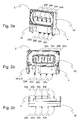
- Fig. 1 shows in a two- and a three-dimensional view of a connector of the inventive arrangement.
- Fig. 2 shows in a two- and two-dimensional views of an inventive arrangement of a connector and a ferrite core, however, without the associated circuit board.
- Fig. 3 shows a two-dimensional view of an inventive arrangement with circuit board, a connector and a ferrite core.
- Fig. 1 shows in a two- and a three-dimensional front view of a connector (2) of the arrangement according to the invention.
- a connector (2) shown from the perspective of its potential connection partner, which a plurality, here four, line elements (20 ad, see. Fig. 3 ) and a molded body (30) made of an electrically insulating plastic.
- the line elements (20 ad) are formed as stamped metal moldings and arranged in series at equal intervals. They are partially enclosed by the plastic molding (30) for their positioning.
- the first ends (22 ad) of the respective line element (20 ad) each form a first contact means to a circuit board (1, see. Fig. 3 ) out.
- the respective first contact means (22 ad) is formed as a solder tag.
- the second end (24 ad) of the respective line element (20 ad) forms a second contact means, here a plug.
- the respective sockets as not shown connection partner of this connector are formed according to the grid of the second contact means (24 ad) and formed by the shaped body (30) receptacle.
- plastic molded body (30) still a schematically indicated only sealing means (34) to the second contact means (24 a-d) arranged around, on to protect the connector to the connection partner, not shown against moisture.
- Fig. 1b shows the described connector (2) in a three-dimensional view, wherein the configuration of the line elements (20 ad) as a flat metal moldings with first (22 ad) and second contact means (24 ad) is clear.
- Fig. 2 shows in a two- and two-dimensional views of an inventive arrangement of a connector (2) and a ferrite core (4) but without the associated circuit board.
- This ferrite core (4) surrounds here three of the four line elements (20 ad).
- the molded body (30) of the connector (2) is designed such that the ferrite core (4) on sections (26 ad) of the line elements from the direction of the first contact devices (22 ad) can be plugged.
- the plastic molding (30) in a region (32) adjacent to the first contact means (22 ad) freed, whereby the line elements (20 a-) are arranged side by side without further insulating material.
- this ferrite core (4) does not necessarily surround all the line elements (20 ad), as in the rear view according to FIG Fig. 2b illustrated. Due to the design of the molded body (30) with the recess (32), the position of the ferrite core (4) can be determined during the construction of the inventive arrangements. Thus, various configurations with one or more ferrite cores (4) to any number of line elements (20 ad) arranged possible, wherein the respective specific embodiment does not need to be determined during the production of the connector (2).
- the ferrite core (4) is designed as a hollow cylinder with a rectangular base, because it can thus be arranged as compactly as possible around the line elements (20 ad) to be surrounded. It is further essential for this that the ferrite core (4) has a specific resistance (p) greater than 10 7 ⁇ m and a relative permeability ( ⁇ r ) greater than 200.
- Fig. 3 shows in a two-dimensional rear view of an inventive arrangement with circuit board (1), connector (2) and ferrite core (4). Shown here are two connecting elements (36) of the insulating molded body (30) for the mechanical connection of the connector (2) with the circuit board (1). Likewise apparent is the connection of the first contact devices (22 ad) of the line elements (20 ad) of the connector (2) with the printed circuit board (1) or with connecting means (10 ad) on printed conductors of the printed circuit board (1).
- the ferrite core (4) rests directly on the printed circuit board (1), but this is not necessarily advantageous for the simple production of the arrangements according to the invention. It is also advantageous here if the height of the ferrite core (4) is less than the height of the recess (32) in the molded body (30).
- the advantageous embodiment of the connector (2) relative to the circuit board (1) wherein the line elements (20 ad) in the initial course starting with the first contact device (22 ad) perpendicular to the circuit board (1) protrude and are arranged parallel to each other and in the further course to the second contact device (24 ad) parallel to each other and the circuit board (1) are arranged.
Abstract
Description
Die Erfindung beschreibt eine Anordnung mit einer Leiterplatte, mindestens einem Steckverbinder und mindestens einem diesem Steckverbinder zugeordneten Ferritkern. Derartige Anordnungen finden beispielhaft Verwendung bei leistungselektronischen Ansteuerschaltungen und deren Verbindungen zu als Motor oder Generator betriebenen elektrischen Maschinen.The invention describes an arrangement with a printed circuit board, at least one connector and at least one ferrite core associated with this connector. Such arrangements find exemplary use in power electronic drive circuits and their connections to operated as a motor or generator electrical machines.
Aufgrund der häufigen und hohen auftretenden Änderungen der Spannungen auf den Verbindungsleitungen zwischen der Ansteuerschaltung und der elektrischen Maschine ist es aus Gründen der elektromagnetischen Verträglichkeit unumgänglich passive Filtereinrichtungen vorzusehen.Due to the frequent and high occurring changes in the voltages on the connecting lines between the drive circuit and the electric machine, it is imperative to provide passive filter devices for reasons of electromagnetic compatibility.
Aus vielfältigen Anwendungen in der Elektrotechnik sind Ferritkerne als Mantelwellenfilter in Kabelverbindungen bekannt. Hierbei sind die Ferritkerne häufig nahe benachbart den Steckverbindungen der Kabelverbindungen angeordnet und umschließend hierbei alle Einzeldrähte der Kabelverbindung. Somit unterdrücken die Ferritkerne wirksam die Gleichtaktstörungen der Kabelverbindung.Ferrite cores are known as sheath wave filters in cable connections for a variety of applications in electrical engineering. In this case, the ferrite cores are often arranged close to the connectors of the cable connections and enclosing all individual wires of the cable connection. Thus, the ferrite cores effectively suppress the common mode noise of the cable joint.
In der
Im Rahmen der
Der Erfindung liegt die Aufgabe zugrunde eine Anordnung mit Leiterplatte, mindestens einem Steckverbinder und mindestens einem diesem zugeordneten Ferritkern anzugeben, wobei die Lage des Ferritkerns flexibel, bei der Anordnung des Steckverbinders auf der Leiterplatte, gewählt kann und wobei die Anordnung eine ausreichende Dämpfung bereit stellt.The invention has for its object an arrangement with printed circuit board, indicate at least one connector and at least one associated ferrite core, wherein the position of the ferrite core flexible, in the arrangement of the connector on the circuit board, can be selected and wherein the arrangement provides sufficient damping.
Diese Aufgabe wird erfindungsgemäß gelöst, durch eine Anordnung mit den Merkmalen des Anspruchs 1. Bevorzugte Ausführungsformen sind in den abhängigen Ansprüchen beschrieben.This object is achieved by an arrangement with the features of
Ausgangspunkt der erfindungsgemäßen Anordnung ist eine Ansteuerschaltung für leistungselektronische Systeme. Eine derartige Ansteuerschaltungen weist neben weiteren Bauelementen eine Anordnung bestehend aus einer Leiterplatte, mindestens einem Steckverbinder und mindestens einem diesen Steckverbinder zugeordneten Ferritkern auf. Erfindungsgemäß weist der Steckverbinder eine Mehrzahl von Leitungselementen mit ersten und zweiten Kontakteinrichtungen auf, wobei diese Leitungselemente mittels eines isolierenden, vorzugsweise aus einem thermoplasten Kunststoff bestehenden, Formkörpers zueinander angeordnet sind. Hierdurch werden die Leitungselemente gegeneinander elektrisch isoliert und sind teilweise von dem Formkörper umschlossen, wobei der Formkörper mindestens eine Aussparung aufweist, damit neben Kontakteinrichtungen weitere erste Abschnitte der Leitungselemente freigespart, also nicht umschlossen, sind.The starting point of the arrangement according to the invention is a drive circuit for power electronic systems. Such a drive circuit has, in addition to other components, an arrangement consisting of a printed circuit board, at least one connector and at least one ferrite core associated with this connector. According to the invention, the plug connector has a plurality of line elements with first and second contact devices, wherein these line elements are arranged relative to one another by means of an insulating, preferably made of a thermoplastic plastic, molded body. As a result, the line elements are electrically insulated from each other and are partially enclosed by the shaped body, wherein the shaped body has at least one recess, so that in addition to contact devices further first sections of the line elements freed, that is not enclosed, are.
In diesem nicht von dem Formkörper umschlossenen Bereich des Steckverbinders sind mindestens zwei benachbarte, aber vorzugsweise nicht alle ersten Abschnitte von Leitungselementen von einem zumindest teilweise direkt an den Abschnitten der Leitungselemente anliegenden Ferritkern umschlossen. Weiterhin weisen die Leitungselemente des Steckverbinders ersten Kontakteinrichtungen auf, die mit dritten Kontakteinrichtungen der Leiterplatte elektrisch leitend verbunden sind. Zweite Kontakteinrichtungen der Leitungselemente des Steckverbinders bilden einen Stecker oder eine Steckhülse aus und dienen dem Anschluss mittels Steckhülse oder Stecker eines Kabels.In this region of the connector, which is not enclosed by the molded body, at least two adjacent, but preferably not all, first portions of conduit elements are enclosed by a ferrite core, which bears at least partially directly on the sections of the conduit elements. Furthermore, the line elements of the connector on first contact means, which are electrically connected to third contact means of the circuit board. Second contact means of the line elements of the connector form a plug or a receptacle and serve the connection by means of a plug or plug of a cable.
Es ist hierbei besonders bevorzugt, wenn der Formkörper des Steckverbinders derart ausgebildet ist, dass der Ferritkern auf die Abschnitte der Leitungselemente des konfektionierten Steckverbinders aufsteckbar ist. Da derartige Leitungselemente meist einen rechteckigen Querschnitt aufweisen und senkrecht von der Leiterplatte wegstehen ist es weiterhin bevorzugt, wenn der Ferritkern als Hohlquader mit rechteckiger Grundfläche ausgebildet ist. Somit können alle Innenflächen des als Hohlquader ausgebildeten Ferritkerns an den ersten Abschnitten der umschlossenen Leitungselemente anliegen. Hierbei ist es besonders bevorzugt, wenn der Ferritkern einen spezifischen Widerstand (p) größer als 107 Ωm und eine relative Permeabilität (µr) größer als 200 aufweist.It is particularly preferred in this case if the shaped body of the connector is designed such that the ferrite core can be plugged onto the sections of the line elements of the assembled connector. Since such line elements usually have a rectangular cross-section and perpendicularly protrude from the circuit board, it is further preferred if the ferrite core is formed as a hollow cuboid with a rectangular base. Thus, all inner surfaces of the ferrite core formed as a hollow cuboid can rest against the first sections of the enclosed line elements. In this case, it is particularly preferred if the ferrite core has a specific resistance (p) greater than 10 7 Ωm and a relative permeability (μ r ) greater than 200.
Besonders bevorzugte Weiterbildungen dieser Anordnung sind in der jeweiligen Beschreibung der Ausführungsbeispiele genannt. Die erfinderische Lösung wird zudem an Hand der Ausführungsbeispiele der
Die Leitungselemente (20 a-d) sind als gestanzte Metallformkörper ausgebildet und in Reihe mit gleichen Abständen angeordnet. Sie werden zu ihrer Positionierung teilweise von dem Kunststoffformkörper (30) umschlossen. Die ersten Enden (22 a-d) des jeweiligen Leitungselements (20 a-d) bilden jeweils eine erste Kontakteinrichtungen zu einer Leiterplatte (1, vgl.
Zusätzlich weist der Kunststoffformkörper (30) noch eine nur schematisch angedeutete Dichteinrichtung (34), um die zweiten Kontakteinrichtungen (24 a-d) herum angeordnet, auf, um die Steckverbindung zum nicht dargestellten Verbindungspartner gegen Feuchtigkeit zu schützen.In addition, the plastic molded body (30) still a schematically indicated only sealing means (34) to the second contact means (24 a-d) arranged around, on to protect the connector to the connection partner, not shown against moisture.
Der Formkörper (30) des Steckverbinders (2) ist derart ausgebildet, dass der Ferritkern (4) auf Abschnitte (26 a-d) der Leitungselemente aus Richtung der ersten Kontakteinrichtungen (22 a-d) aufsteckbar ist. Hierzu ist der Kunststoffformkörper (30) in einem Bereich (32) angrenzend an die ersten Kontakteinrichtungen (22 a-d) freigespart, wodurch die Leitungselemente (20 a-) ohne weiteren lsolationsstoff nebeneinander angeordnet sind.The molded body (30) of the connector (2) is designed such that the ferrite core (4) on sections (26 ad) of the line elements from the direction of the first contact devices (22 ad) can be plugged. For this purpose, the plastic molding (30) in a region (32) adjacent to the first contact means (22 ad) freed, whereby the line elements (20 a-) are arranged side by side without further insulating material.
Wesentlich für die Erfindung ist, dass dieser Ferritkern (4) nicht notwendigerweise alle Leitungselemente (20 a-d) umschließt, wie in der Rückansicht gemäß
Für die genannte Ausgestaltung ist es besonders vorteilhaft, wenn der Ferritkern (4) als Hohlzylinder mit rechteckiger Grundfläche ausgebildet ist, weil er somit möglichst kompakt um die zu umschließenden Leitungselemente (20 a-d) herum angeordnet werden kann. Hierzu ist weiterhin wesentlich, dass der Ferritkern (4) einen spezifischen Widerstand (p) größer als 107 Ωm und eine relative Permeabilität (µr) größer als 200 aufweist.For the embodiment mentioned, it is particularly advantageous if the ferrite core (4) is designed as a hollow cylinder with a rectangular base, because it can thus be arranged as compactly as possible around the line elements (20 ad) to be surrounded. It is further essential for this that the ferrite core (4) has a specific resistance (p) greater than 10 7 Ωm and a relative permeability (μ r ) greater than 200.
Dank dieser physikalischen Daten der Ausgestaltung des Ferritkerns (4) ist es möglich, dass der Innenzylinder des als Hohlquader ausgebildeten Ferritkerns (4) allseits an den ersten Abschnitten (26 a-d) der umschlossenen Leitungselemente anliegt, wie dies auch in der Draufsicht gemäß
Hierbei ist ebenfalls ersichtlich, dass der Ferritkern (4) unmittelbar an der Leiterplatte (1) anliegt, dies ist nicht notwendig allerdings vorteilhaft für die einfache Herstellung der erfindungsgemäßen Anordnungen. Hierbei ist es ebenfalls vorteilhaft, wenn die Höhe des Ferritkerns (4) geringer ist als die Höhe der Aussparung (32) im Formkörper (30).It can also be seen here that the ferrite core (4) rests directly on the printed circuit board (1), but this is not necessarily advantageous for the simple production of the arrangements according to the invention. It is also advantageous here if the height of the ferrite core (4) is less than the height of the recess (32) in the molded body (30).
Weiterhin dargestellt ist die vorteilhafte Ausgestaltung des Steckverbinders (2) relativ zur Leiterplatte (1), wobei die Leitungselemente (20 a-d) im anfänglichen Verlauf beginnend mit der ersten Kontakteinrichtung (22 a-d) senkrecht von der Leiterplatte (1) wegstehen und parallel zueinander angeordnet sind und im weiteren Verlauf zur zweiten Kontakteinrichtung (24 a-d) parallel zueinander und zur Leiterplatte (1) angeordnet sind.Also shown is the advantageous embodiment of the connector (2) relative to the circuit board (1), wherein the line elements (20 ad) in the initial course starting with the first contact device (22 ad) perpendicular to the circuit board (1) protrude and are arranged parallel to each other and in the further course to the second contact device (24 ad) parallel to each other and the circuit board (1) are arranged.
Claims (8)
wobei der Steckverbinder (2) eine Mehrzahl von Leitungselementen (20 a-d) mit ersten (22 a-d) und zweiten (24 a-d) Kontakteinrichtungen aufweist, diese Leitungselemente (20 a-d) mittels eines isolierenden Formkörpers (30) zueinander angeordnet, hierdurch gegeneinander elektrisch isoliert und teilweise umschlossen werden, wobei der Formkörper (30) erste Abschnitte (24 a-d) der Leitungselemente (20 a-d) freispart und in diesem Bereich (32) des Steckverbinders (30) mindestens zwei benachbarte erste Abschnitte (26 a-d) von Leitungselementen (20 a-d) von einem zumindest teilweise direkt an den ersten Abschnitten (26 a-d) der Leitungselemente (20 a-d) anliegenden Ferritkern (4) umschlossen sind und wobei die ersten Kontakteinrichtungen (22 a-d) mit dritten Kontakteinrichtungen (10 a-d) der Leiterplatte (1) elektrisch leitend verbunden sind sowie die zweiten Kontakteinrichtungen (24 a-d) einen Stecker oder eine Steckhülse ausbilden.Arrangement comprising a printed circuit board (1), a plug connector (2) and at least one ferrite core (4) assigned to this plug connector (2),
wherein the connector (2) has a plurality of line elements (20 ad) with first (22 ad) and second (24 ad) contact means, these line elements (20 ad) by means of an insulating molded body (30) arranged to each other, thereby electrically isolated from each other and partially enclosed, wherein the shaped body (30) frees first sections (24 ad) of the line elements (20 ad) and in this region (32) of the connector (30) at least two adjacent first sections (26 ad) of line elements (20 ad) are enclosed by an at least partially directly to the first portions (26 ad) of the line elements (20 ad) adjacent ferrite core (4) and wherein the first contact means (22 ad) with third contact means (10 ad) of the circuit board (1) electrically conductively connected are and the second contact means (24 ad) form a plug or a socket.
wobei der Formkörper (30) des Steckverbinders (2) derart ausgebildet ist, dass der Ferritkern (4) auf die ersten Abschnitte (26 a-d) der Leitungselemente (20 a-d) aufsteckbar ist.Arrangement according to claim 1
wherein the molded body (30) of the connector (2) is formed such that the ferrite core (4) on the first portions (26 ad) of the line elements (20 ad) can be plugged.
wobei der Ferritkern (4) als Hohlquader mit rechteckiger Grundfläche ausgebildet ist.Arrangement according to claim 1
wherein the ferrite core (4) is formed as a hollow cuboid with a rectangular base.
wobei der Innenzylinder des als Hohlquader ausgebildeten Ferritkerns (4) allseits an den ersten Abschnitten (26 a-d) der umschlossenen Leitungselemente (20 a-d) anliegt.Arrangement according to claim 3
wherein the inner cylinder of the formed as a hollow cuboid ferrite core (4) on all sides at the first portions (26 ad) of the enclosed line elements (20 ad) is applied.
wobei der Ferritkern (4) einen spezifischen Widerstand (p) größer als 107 Ωm und eine relative Permeabilität (µr) größer als 200 aufweist.Arrangement according to claim 1
wherein the ferrite core (4) has a resistivity (p) greater than 10 7 Ωm and a relative permeability (μ r ) greater than 200.
wobei der Ferritkern (4) unmittelbar an der Leiterplatte (1) anliegt.Arrangement according to claim 1
wherein the ferrite core (4) directly against the printed circuit board (1).
wobei der isolierende Formkörper (30) ein Verbindungselement (36) zur mechanischen Verbindung mit der Leiterplatte (1) aufweist und eine Dichteinrichtung (34) um die zweiten Kontakteinrichtungen (24 a-d) herum aufweist.Arrangement according to claim 1
wherein the insulating molding (30) has a connecting element (36) for mechanical connection to the printed circuit board (1) and has a sealing device (34) around the second contact devices (24 ad).
wobei die Leitungselemente (20 a-d) im anfänglichen Verlauf senkrecht von der Leiterplatte (1) wegstehen und parallel zueinander angeordnet sind und im weiteren einen Verlauf parallel zur Leiterplatte (1) aufweisen.Arrangement according to claim 1
wherein the line elements (20 ad) in the initial course perpendicular to the printed circuit board (1) protrude and are arranged parallel to each other and further have a course parallel to the printed circuit board (1).
Applications Claiming Priority (1)
| Application Number | Priority Date | Filing Date | Title |
|---|---|---|---|
| DE102008023715A DE102008023715A1 (en) | 2008-05-15 | 2008-05-15 | Arrangement with printed circuit board, plug connector and ferrite core |
Publications (3)
| Publication Number | Publication Date |
|---|---|
| EP2120295A2 true EP2120295A2 (en) | 2009-11-18 |
| EP2120295A3 EP2120295A3 (en) | 2012-07-04 |
| EP2120295B1 EP2120295B1 (en) | 2015-08-19 |
Family
ID=40673397
Family Applications (1)
| Application Number | Title | Priority Date | Filing Date |
|---|---|---|---|
| EP09005274.7A Active EP2120295B1 (en) | 2008-05-15 | 2009-04-11 | Assembly with circuit board, connector and ferrite core |
Country Status (2)
| Country | Link |
|---|---|
| EP (1) | EP2120295B1 (en) |
| DE (1) | DE102008023715A1 (en) |
Cited By (1)
| Publication number | Priority date | Publication date | Assignee | Title |
|---|---|---|---|---|
| WO2013150103A1 (en) * | 2012-04-04 | 2013-10-10 | Continental Automotive Gmbh | Core for simple attainment of common-mode damping properties in control devices |
Families Citing this family (1)
| Publication number | Priority date | Publication date | Assignee | Title |
|---|---|---|---|---|
| DE102010034517B4 (en) | 2009-08-17 | 2022-10-06 | Sew-Eurodrive Gmbh & Co Kg | Hybrid connector and converter motor with the hybrid connector |
Citations (2)
| Publication number | Priority date | Publication date | Assignee | Title |
|---|---|---|---|---|
| DE9112098U1 (en) | 1991-09-27 | 1993-01-28 | Siemens Ag, 8000 Muenchen, De | |
| DE4326486A1 (en) | 1993-08-06 | 1995-02-09 | Siemens Ag | Filter plug |
Family Cites Families (6)
| Publication number | Priority date | Publication date | Assignee | Title |
|---|---|---|---|---|
| DE9005597U1 (en) * | 1990-05-16 | 1991-09-12 | Siemens Ag, 8000 Muenchen, De | |
| US5224878A (en) * | 1992-03-31 | 1993-07-06 | Amp Incorporated | Connector filter with integral surge protection |
| US5415569A (en) * | 1992-10-19 | 1995-05-16 | Molex Incorporated | Filtered electrical connector assembly |
| EP0732777A3 (en) * | 1995-03-14 | 1997-06-18 | At & T Corp | Electromagnetic interference suppressing connector array |
| DE19611699C1 (en) * | 1996-03-25 | 1997-11-13 | Siemens Ag | Filter plug connector with screened housing e.g.for automobile air-bag control devices |
| JP3494113B2 (en) * | 2000-03-28 | 2004-02-03 | 住友電装株式会社 | connector |
-
2008
- 2008-05-15 DE DE102008023715A patent/DE102008023715A1/en not_active Withdrawn
-
2009
- 2009-04-11 EP EP09005274.7A patent/EP2120295B1/en active Active
Patent Citations (2)
| Publication number | Priority date | Publication date | Assignee | Title |
|---|---|---|---|---|
| DE9112098U1 (en) | 1991-09-27 | 1993-01-28 | Siemens Ag, 8000 Muenchen, De | |
| DE4326486A1 (en) | 1993-08-06 | 1995-02-09 | Siemens Ag | Filter plug |
Cited By (1)
| Publication number | Priority date | Publication date | Assignee | Title |
|---|---|---|---|---|
| WO2013150103A1 (en) * | 2012-04-04 | 2013-10-10 | Continental Automotive Gmbh | Core for simple attainment of common-mode damping properties in control devices |
Also Published As
| Publication number | Publication date |
|---|---|
| EP2120295A3 (en) | 2012-07-04 |
| EP2120295B1 (en) | 2015-08-19 |
| DE102008023715A1 (en) | 2009-12-03 |
Similar Documents
| Publication | Publication Date | Title |
|---|---|---|
| DE102013108383C5 (en) | connector module | |
| EP2883287B1 (en) | System comprising a connector and contact elements | |
| DE112014005282B4 (en) | Shield structure, shield connector and method of manufacturing a shield connector with an electric wire | |
| EP0265698A2 (en) | Connection device for the electrical connection of the connection points of electrical apparatuses | |
| DE2104057A1 (en) | Electrical connector assembly | |
| DE102008050322B4 (en) | Electric motor connection and electric motor | |
| DE3239238A1 (en) | METHOD FOR WIRING ELECTRICAL DEVICES, ESPECIALLY ELECTRIC TOOLS, AND ELECTRICAL DEVICE | |
| DE202006006659U1 (en) | Structural assembly for industrial automation device, has housing half provided with metallic fixing devices for fixing and contacting printed circuit board and coupling part and including connector in base area | |
| DE112010005976T5 (en) | EMC filter circuit | |
| DE202013006295U1 (en) | System with multiple connectors and multiple connectors | |
| DE102012111326A1 (en) | Electric DC motor | |
| EP2933890A1 (en) | Flush mounting of an electrical installation apparatus | |
| DE102005016534B4 (en) | Device with electrical terminals and jumper | |
| DE19627481C2 (en) | Electrical switch and fuse device | |
| EP1959523A1 (en) | Keying device for plug connectors | |
| EP2120295B1 (en) | Assembly with circuit board, connector and ferrite core | |
| DE102008025432A1 (en) | Clamping connection block i.e. motor terminal block, for electrical connection of three-phase motor, has plug parts that are arranged in housing such that plug parts are electrically connected with contacts of connection plugs | |
| EP3241261A1 (en) | Overvoltage protection arrangement for information and telecommunication technology | |
| EP3323176B1 (en) | Plug connector assembly with coding | |
| DE102017111245A1 (en) | power distribution | |
| DE102015110644A1 (en) | Device for separable electrical connection | |
| DE102014115384A1 (en) | Test cable and socket adapter for a test cable | |
| DE102013013715B4 (en) | Electrical contact arrangement and method for producing such an electrical contact arrangement | |
| DE212019000423U1 (en) | Connection device for electrical conductors | |
| DE19715437C2 (en) | Electrical distribution device with common conductor |
Legal Events
| Date | Code | Title | Description |
|---|---|---|---|
| PUAI | Public reference made under article 153(3) epc to a published international application that has entered the european phase |
Free format text: ORIGINAL CODE: 0009012 |
|
| AK | Designated contracting states |
Kind code of ref document: A2 Designated state(s): AT BE BG CH CY CZ DE DK EE ES FI FR GB GR HR HU IE IS IT LI LT LU LV MC MK MT NL NO PL PT RO SE SI SK TR |
|
| PUAL | Search report despatched |
Free format text: ORIGINAL CODE: 0009013 |
|
| REG | Reference to a national code |
Ref country code: DE Ref legal event code: R079 Ref document number: 502009011430 Country of ref document: DE Free format text: PREVIOUS MAIN CLASS: H01R0012200000 Ipc: H01R0012720000 |
|
| AK | Designated contracting states |
Kind code of ref document: A3 Designated state(s): AT BE BG CH CY CZ DE DK EE ES FI FR GB GR HR HU IE IS IT LI LT LU LV MC MK MT NL NO PL PT RO SE SI SK TR |
|
| AX | Request for extension of the european patent |
Extension state: AL BA RS |
|
| RIC1 | Information provided on ipc code assigned before grant |
Ipc: H01R 12/72 20110101AFI20120608BHEP |
|
| 17P | Request for examination filed |
Effective date: 20130104 |
|
| 17Q | First examination report despatched |
Effective date: 20140212 |
|
| GRAP | Despatch of communication of intention to grant a patent |
Free format text: ORIGINAL CODE: EPIDOSNIGR1 |
|
| GRAS | Grant fee paid |
Free format text: ORIGINAL CODE: EPIDOSNIGR3 |
|
| INTG | Intention to grant announced |
Effective date: 20150615 |
|
| GRAA | (expected) grant |
Free format text: ORIGINAL CODE: 0009210 |
|
| AK | Designated contracting states |
Kind code of ref document: B1 Designated state(s): AT BE BG CH CY CZ DE DK EE ES FI FR GB GR HR HU IE IS IT LI LT LU LV MC MK MT NL NO PL PT RO SE SI SK TR |
|
| REG | Reference to a national code |
Ref country code: GB Ref legal event code: FG4D Free format text: NOT ENGLISH |
|
| REG | Reference to a national code |
Ref country code: CH Ref legal event code: EP |
|
| REG | Reference to a national code |
Ref country code: IE Ref legal event code: FG4D Free format text: LANGUAGE OF EP DOCUMENT: GERMAN |
|
| REG | Reference to a national code |
Ref country code: AT Ref legal event code: REF Ref document number: 744374 Country of ref document: AT Kind code of ref document: T Effective date: 20150915 |
|
| REG | Reference to a national code |
Ref country code: DE Ref legal event code: R096 Ref document number: 502009011430 Country of ref document: DE |
|
| REG | Reference to a national code |
Ref country code: LT Ref legal event code: MG4D |
|
| REG | Reference to a national code |
Ref country code: NL Ref legal event code: MP Effective date: 20150819 |
|
| PG25 | Lapsed in a contracting state [announced via postgrant information from national office to epo] |
Ref country code: NO Free format text: LAPSE BECAUSE OF FAILURE TO SUBMIT A TRANSLATION OF THE DESCRIPTION OR TO PAY THE FEE WITHIN THE PRESCRIBED TIME-LIMIT Effective date: 20151119 Ref country code: LT Free format text: LAPSE BECAUSE OF FAILURE TO SUBMIT A TRANSLATION OF THE DESCRIPTION OR TO PAY THE FEE WITHIN THE PRESCRIBED TIME-LIMIT Effective date: 20150819 Ref country code: FI Free format text: LAPSE BECAUSE OF FAILURE TO SUBMIT A TRANSLATION OF THE DESCRIPTION OR TO PAY THE FEE WITHIN THE PRESCRIBED TIME-LIMIT Effective date: 20150819 Ref country code: GR Free format text: LAPSE BECAUSE OF FAILURE TO SUBMIT A TRANSLATION OF THE DESCRIPTION OR TO PAY THE FEE WITHIN THE PRESCRIBED TIME-LIMIT Effective date: 20151120 Ref country code: LV Free format text: LAPSE BECAUSE OF FAILURE TO SUBMIT A TRANSLATION OF THE DESCRIPTION OR TO PAY THE FEE WITHIN THE PRESCRIBED TIME-LIMIT Effective date: 20150819 |
|
| PG25 | Lapsed in a contracting state [announced via postgrant information from national office to epo] |
Ref country code: PL Free format text: LAPSE BECAUSE OF FAILURE TO SUBMIT A TRANSLATION OF THE DESCRIPTION OR TO PAY THE FEE WITHIN THE PRESCRIBED TIME-LIMIT Effective date: 20150819 Ref country code: IS Free format text: LAPSE BECAUSE OF FAILURE TO SUBMIT A TRANSLATION OF THE DESCRIPTION OR TO PAY THE FEE WITHIN THE PRESCRIBED TIME-LIMIT Effective date: 20151219 Ref country code: ES Free format text: LAPSE BECAUSE OF FAILURE TO SUBMIT A TRANSLATION OF THE DESCRIPTION OR TO PAY THE FEE WITHIN THE PRESCRIBED TIME-LIMIT Effective date: 20150819 Ref country code: SE Free format text: LAPSE BECAUSE OF FAILURE TO SUBMIT A TRANSLATION OF THE DESCRIPTION OR TO PAY THE FEE WITHIN THE PRESCRIBED TIME-LIMIT Effective date: 20150819 Ref country code: PT Free format text: LAPSE BECAUSE OF FAILURE TO SUBMIT A TRANSLATION OF THE DESCRIPTION OR TO PAY THE FEE WITHIN THE PRESCRIBED TIME-LIMIT Effective date: 20151221 |
|
| PG25 | Lapsed in a contracting state [announced via postgrant information from national office to epo] |
Ref country code: NL Free format text: LAPSE BECAUSE OF FAILURE TO SUBMIT A TRANSLATION OF THE DESCRIPTION OR TO PAY THE FEE WITHIN THE PRESCRIBED TIME-LIMIT Effective date: 20150819 |
|
| REG | Reference to a national code |
Ref country code: FR Ref legal event code: PLFP Year of fee payment: 8 |
|
| PG25 | Lapsed in a contracting state [announced via postgrant information from national office to epo] |
Ref country code: SK Free format text: LAPSE BECAUSE OF FAILURE TO SUBMIT A TRANSLATION OF THE DESCRIPTION OR TO PAY THE FEE WITHIN THE PRESCRIBED TIME-LIMIT Effective date: 20150819 Ref country code: CZ Free format text: LAPSE BECAUSE OF FAILURE TO SUBMIT A TRANSLATION OF THE DESCRIPTION OR TO PAY THE FEE WITHIN THE PRESCRIBED TIME-LIMIT Effective date: 20150819 Ref country code: EE Free format text: LAPSE BECAUSE OF FAILURE TO SUBMIT A TRANSLATION OF THE DESCRIPTION OR TO PAY THE FEE WITHIN THE PRESCRIBED TIME-LIMIT Effective date: 20150819 Ref country code: DK Free format text: LAPSE BECAUSE OF FAILURE TO SUBMIT A TRANSLATION OF THE DESCRIPTION OR TO PAY THE FEE WITHIN THE PRESCRIBED TIME-LIMIT Effective date: 20150819 Ref country code: IT Free format text: LAPSE BECAUSE OF FAILURE TO SUBMIT A TRANSLATION OF THE DESCRIPTION OR TO PAY THE FEE WITHIN THE PRESCRIBED TIME-LIMIT Effective date: 20150819 |
|
| REG | Reference to a national code |
Ref country code: DE Ref legal event code: R097 Ref document number: 502009011430 Country of ref document: DE |
|
| PG25 | Lapsed in a contracting state [announced via postgrant information from national office to epo] |
Ref country code: RO Free format text: LAPSE BECAUSE OF FAILURE TO SUBMIT A TRANSLATION OF THE DESCRIPTION OR TO PAY THE FEE WITHIN THE PRESCRIBED TIME-LIMIT Effective date: 20150819 |
|
| PLBE | No opposition filed within time limit |
Free format text: ORIGINAL CODE: 0009261 |
|
| STAA | Information on the status of an ep patent application or granted ep patent |
Free format text: STATUS: NO OPPOSITION FILED WITHIN TIME LIMIT |
|
| 26N | No opposition filed |
Effective date: 20160520 |
|
| PG25 | Lapsed in a contracting state [announced via postgrant information from national office to epo] |
Ref country code: SI Free format text: LAPSE BECAUSE OF FAILURE TO SUBMIT A TRANSLATION OF THE DESCRIPTION OR TO PAY THE FEE WITHIN THE PRESCRIBED TIME-LIMIT Effective date: 20150819 Ref country code: BE Free format text: LAPSE BECAUSE OF NON-PAYMENT OF DUE FEES Effective date: 20160430 |
|
| REG | Reference to a national code |
Ref country code: CH Ref legal event code: PL |
|
| PG25 | Lapsed in a contracting state [announced via postgrant information from national office to epo] |
Ref country code: LU Free format text: LAPSE BECAUSE OF FAILURE TO SUBMIT A TRANSLATION OF THE DESCRIPTION OR TO PAY THE FEE WITHIN THE PRESCRIBED TIME-LIMIT Effective date: 20160411 |
|
| REG | Reference to a national code |
Ref country code: IE Ref legal event code: MM4A |
|
| PG25 | Lapsed in a contracting state [announced via postgrant information from national office to epo] |
Ref country code: CH Free format text: LAPSE BECAUSE OF NON-PAYMENT OF DUE FEES Effective date: 20160430 Ref country code: LI Free format text: LAPSE BECAUSE OF NON-PAYMENT OF DUE FEES Effective date: 20160430 |
|
| REG | Reference to a national code |
Ref country code: FR Ref legal event code: PLFP Year of fee payment: 9 |
|
| PG25 | Lapsed in a contracting state [announced via postgrant information from national office to epo] |
Ref country code: IE Free format text: LAPSE BECAUSE OF NON-PAYMENT OF DUE FEES Effective date: 20160411 |
|
| REG | Reference to a national code |
Ref country code: AT Ref legal event code: MM01 Ref document number: 744374 Country of ref document: AT Kind code of ref document: T Effective date: 20160411 |
|
| PG25 | Lapsed in a contracting state [announced via postgrant information from national office to epo] |
Ref country code: AT Free format text: LAPSE BECAUSE OF NON-PAYMENT OF DUE FEES Effective date: 20160411 |
|
| REG | Reference to a national code |
Ref country code: FR Ref legal event code: PLFP Year of fee payment: 10 |
|
| PG25 | Lapsed in a contracting state [announced via postgrant information from national office to epo] |
Ref country code: CY Free format text: LAPSE BECAUSE OF FAILURE TO SUBMIT A TRANSLATION OF THE DESCRIPTION OR TO PAY THE FEE WITHIN THE PRESCRIBED TIME-LIMIT Effective date: 20150819 Ref country code: HU Free format text: LAPSE BECAUSE OF FAILURE TO SUBMIT A TRANSLATION OF THE DESCRIPTION OR TO PAY THE FEE WITHIN THE PRESCRIBED TIME-LIMIT; INVALID AB INITIO Effective date: 20090411 |
|
| PG25 | Lapsed in a contracting state [announced via postgrant information from national office to epo] |
Ref country code: MC Free format text: LAPSE BECAUSE OF FAILURE TO SUBMIT A TRANSLATION OF THE DESCRIPTION OR TO PAY THE FEE WITHIN THE PRESCRIBED TIME-LIMIT Effective date: 20150819 Ref country code: TR Free format text: LAPSE BECAUSE OF FAILURE TO SUBMIT A TRANSLATION OF THE DESCRIPTION OR TO PAY THE FEE WITHIN THE PRESCRIBED TIME-LIMIT Effective date: 20150819 Ref country code: MT Free format text: LAPSE BECAUSE OF FAILURE TO SUBMIT A TRANSLATION OF THE DESCRIPTION OR TO PAY THE FEE WITHIN THE PRESCRIBED TIME-LIMIT Effective date: 20150819 Ref country code: MK Free format text: LAPSE BECAUSE OF FAILURE TO SUBMIT A TRANSLATION OF THE DESCRIPTION OR TO PAY THE FEE WITHIN THE PRESCRIBED TIME-LIMIT Effective date: 20150819 Ref country code: HR Free format text: LAPSE BECAUSE OF FAILURE TO SUBMIT A TRANSLATION OF THE DESCRIPTION OR TO PAY THE FEE WITHIN THE PRESCRIBED TIME-LIMIT Effective date: 20150819 |
|
| PG25 | Lapsed in a contracting state [announced via postgrant information from national office to epo] |
Ref country code: BG Free format text: LAPSE BECAUSE OF FAILURE TO SUBMIT A TRANSLATION OF THE DESCRIPTION OR TO PAY THE FEE WITHIN THE PRESCRIBED TIME-LIMIT Effective date: 20150819 |
|
| PGFP | Annual fee paid to national office [announced via postgrant information from national office to epo] |
Ref country code: FR Payment date: 20230417 Year of fee payment: 15 Ref country code: DE Payment date: 20230430 Year of fee payment: 15 |
|
| PGFP | Annual fee paid to national office [announced via postgrant information from national office to epo] |
Ref country code: GB Payment date: 20230420 Year of fee payment: 15 |