EP2118941B1 - Supraconducteur soudé avec isolation rigide - Google Patents
Supraconducteur soudé avec isolation rigide Download PDFInfo
- Publication number
- EP2118941B1 EP2118941B1 EP08724435.6A EP08724435A EP2118941B1 EP 2118941 B1 EP2118941 B1 EP 2118941B1 EP 08724435 A EP08724435 A EP 08724435A EP 2118941 B1 EP2118941 B1 EP 2118941B1
- Authority
- EP
- European Patent Office
- Prior art keywords
- accordance
- solder
- composite
- wire
- insulation
- Prior art date
- Legal status (The legal status is an assumption and is not a legal conclusion. Google has not performed a legal analysis and makes no representation as to the accuracy of the status listed.)
- Active
Links
Images

Classifications
-
- H—ELECTRICITY
- H10—SEMICONDUCTOR DEVICES; ELECTRIC SOLID-STATE DEVICES NOT OTHERWISE PROVIDED FOR
- H10N—ELECTRIC SOLID-STATE DEVICES NOT OTHERWISE PROVIDED FOR
- H10N60/00—Superconducting devices
- H10N60/01—Manufacture or treatment
- H10N60/0156—Manufacture or treatment of devices comprising Nb or an alloy of Nb with one or more of the elements of group IVB, e.g. titanium, zirconium or hafnium
-
- Y—GENERAL TAGGING OF NEW TECHNOLOGICAL DEVELOPMENTS; GENERAL TAGGING OF CROSS-SECTIONAL TECHNOLOGIES SPANNING OVER SEVERAL SECTIONS OF THE IPC; TECHNICAL SUBJECTS COVERED BY FORMER USPC CROSS-REFERENCE ART COLLECTIONS [XRACs] AND DIGESTS
- Y10—TECHNICAL SUBJECTS COVERED BY FORMER USPC
- Y10T—TECHNICAL SUBJECTS COVERED BY FORMER US CLASSIFICATION
- Y10T29/00—Metal working
- Y10T29/49—Method of mechanical manufacture
- Y10T29/49002—Electrical device making
- Y10T29/49014—Superconductor
-
- Y—GENERAL TAGGING OF NEW TECHNOLOGICAL DEVELOPMENTS; GENERAL TAGGING OF CROSS-SECTIONAL TECHNOLOGIES SPANNING OVER SEVERAL SECTIONS OF THE IPC; TECHNICAL SUBJECTS COVERED BY FORMER USPC CROSS-REFERENCE ART COLLECTIONS [XRACs] AND DIGESTS
- Y10—TECHNICAL SUBJECTS COVERED BY FORMER USPC
- Y10T—TECHNICAL SUBJECTS COVERED BY FORMER US CLASSIFICATION
- Y10T29/00—Metal working
- Y10T29/49—Method of mechanical manufacture
- Y10T29/49002—Electrical device making
- Y10T29/49117—Conductor or circuit manufacturing
- Y10T29/49174—Assembling terminal to elongated conductor
- Y10T29/49176—Assembling terminal to elongated conductor with molding of electrically insulating material
Definitions
- This invention relates generally to the manufacture of superconductors, and more specifically, relates to a method enabling the addition of a hard insulation film to a multifilamentary superconductor that has been soldered to a large amount of copper, thus minimizing production cost and giving increased control of copper content.
- a hard insulation film gives the minimum insulation layer thickness, thus maximizing conductor volume for use in a electromagnetic coil.
- Superconducting wire composites used in electromagnets consist of a multifilamentary superconductor, copper stabilizing matrix, and an outer electrical insulation layer.
- the superconducting alloy in the multifilamentary strand is usually niobium titanium.
- the electrical insulation layer on the superconductor wire is critical to its proper performance in most applications. This is particularly true in the construction of solenoid magnets, where multiple layers of wire are wound together under high winding tensions. Tum-to-tum or layer-to-layer electrical shorts seriously degrade performance, and must be prevented.
- a high volume fraction of copper stabilizer is often needed for optimal magnet performance.
- the most cost effective way to produce a conductor having a high copper content is to make a composite of multifilamentary superconductor containing a small volume fraction of copper matrix, and then join it with a large amount of additional copper at the final stage of manufacturing.
- the most common method to integrate the components is soldering.
- the majority of superconductor composite used for MRI is made by soldering a low copper content superconducting strand into the round groove of a relatively large volume generally rectangular shaped copper channel. This process has been referred to as "wire-in-channel".
- These conductors are usually insulated with glass or polymer braid, or tape.
- JP H04 106809 discloses joining a stabilizing metal and an Nb-Ti alloy superconducting wire with a brazing filler metal whose melting point is of 320°C-620°C.
- Formvar® had not been successfully applied to a soldered composite super -conductor used in MRI magnets, because of the low 181 °C melting point of the eutectic Pb-Sn solder alloy. A number of attempts had been made to modify the Formvar® formulations and application processes themselves, without success.
- the conductor is coated with liquid Formvar®, and then the coated composite passes through a heat treatment tower furnace at a temperature significantly higher than the solder melting temperature. This causes the Sn-Pb solder to melt, disrupting the composite bonding, and creates bubbles in the insulating film, preventing proper application and adherence of the insulation.
- the present invention overcomes the problems listed above by use of a high melting point solder to bond the superconductor strand to a solderable metallic component such as a copper channel, as defined in the method of claim 1.
- the solder must be able to withstand, without re-melting, the exposure to the elevated temperature and environment in the insulation processing tower.
- the temperature at which the solder melts is critical to the proper application of the insulating film.
- soldered conductor can be successfully coated with film insulation. While the temperature in the processing tower may be twice the melting point of even the high temperature solder, one can limit the transit time of the composite. This process results in the actual temperature of the composite being brought into the range of -200°C, i.e. in the range that would melt a eutectic Sn-Pb solder but not a high temperature solder, yet is still suitable for curing the Formvar® layer.
- the superconducting composite of choice for soldering into the channel is typically Nb-Ti in a Cu matrix, although a Cu-Ni matrix may be chosen.
- the strand is round in cross-section but a rectangular cross-section conductor may also be used.
- the high copper fraction composite is made by bonding a shaped channel to the superconducting core, but a copper strip instead could be wrapped around the superconducting core.
- solder selection critically depends on the amount of intermetallic formation during the superconducting strand-to-copper channel solder bonding operation, and any subsequent thermal treatment the conductor may undergo.
- An interface layer thickness of 1-3 ⁇ m (microns) between the solder and copper composite superconductor is ideal for most solder operations to obtain the maximum solder bond strength.
- An intermetallic layer much thicker could result in a brittle interface.
- Solder selection is also critical in that full and even filling of the groove in the channel is necessary to prevent eventual bubble formation in the insulation layer. This is controlled by the wetting and surface tension characteristics of the solder alloy, and the degree of superheat used in the soldering process.
- thermo-mechanical fatigue properties are required to ensure that neither the varnish nor solder bond rupture during cycling of the device from room temperature to liquid helium temperature, or that the various films themselves do not undergo fatigue causing failure of the conductor or insulation.
- the coefficient of thermal expansion is important so that the composite does not undergo excessive strain on cooling down to liquid helium temperature (4.2K). It is not necessary to determine the actual coefficient of temperature expansion but only to cycle the coated conductor repeatedly from room temperature to liquid helium temperature and evaluate the adherence of the insulating film.
- solder alloys containing Sn, Ag, Sb, and Cu with higher melting temperatures are all suitable for this application. This is even true for alloys with a relatively low liquidus but high solidus temperature. The alloy will not flow in the intermediate liquidus/solidus range due to the high viscosity. Generally solder having a high Pb content melts at higher temperature, but the use of Pb is not environmentally friendly, and its use is being restricted by legislation in many regions.
- solder to the copper base metal is very important since any trapped gas in voids can outgas during the Formvar® curing process and prohibit bonding of insulation to conductor. Tin rich solders tend to have excellent wettability.
- suitable alloys are given in Table 1. It should be noted that any solder employed cannot have a melting point far above 300°C as this would degrade the superconducting properties of the niobium-titanium alloy in the wire. Also, any solder alloy under consideration should be evaluated for "tin pest", the transformation of the crystal structure of tin to the brittle diamond cubic structure (gray tin ⁇ , a semiconductor). This must be avoided, and has been known to occur in lead-free solders.
- Table 1 TIN-BASED SOLDER ALLOYS HAVING A HIGH TEMPERATURE MELTING RANGE Nominal Composition, % by weight Melting Temperature Range Sn Ag Cu Sb C° 95 5 232°-240° 98 2 221 °-226° 99.3 0.7 227° liquidus 95.5 3.8 0.7 220° liquidus 95 4 1 220° 93.6 4.7 1.7 244° 65 25 10 233° 95.5 0.5 4 217°-350°
- the surface roughness of the solder-coated superconducting composite is important only when the adherence of the film is marginal. Providing a rough surface allows the insulating varnish to mechanically grip the surface and provide a better bond.
- the surface modification can be done by any of the conventional techniques such as abrasion with sandpaper, grit blasting, or embossing. When grit blasting is applied, the composition of the grit and the angle that it is applied is important in providing the best bonding surface, and this depends on the particular varnish and solder combination.
- the embossing can be done prior to, during or after the soldering operation. Surface roughness can also be obtained by the selection of the dies used for shaping after the soldering and via the quenching operations on the soldering line. It is also possible to remove by electroplating off the surface solder (but not the solder bonding the core to the channel) to have a cleaner surface for insulation application.
- the polymer hard insulation coating can be an epoxy, enamel or varnish type insulation with a curing temperature of over 300°C.
- the polymer can be applied by running the soldered strand through a tank of liquid insulation or by extruding the insulation with the strand.
- extrudable polymers include nylon, epoxy, PVC, polyethylene and floro-chloro-carbons.
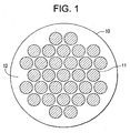
- a multifilamentary superconducting composite is created as shown by the example illustrated in figure 1 , where multiple Nb-Ti alloy rods 11 are stacked into drilled copper billets 12, lids and cones are welded to the billet ends to facilitate extrusion, and the billets are extruded to form the multifilamentary rod 10.
- This multifilamentary rod is reduced from typically 76mm (3") diameter to wire about 500 ⁇ m (0.02") diameter by rod and wiredrawing techniques familiar to those skilled in the art.
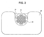
- this multifilamentary superconducting wire 10 is soldered into a copper channel 20 with a high temperature solder 21, with examples of valid selections of solder being shown in (but not limited to) those in Table 1.
- Solder application can be effected by passing the assembly of rod 10 and channel 20 through a solder pot as is known in the art, or other known techniques can be used to apply the solder. It is necessary that the solder 21 evenly fills the channel groove 22 to prevent bubble formation during the subsequent insulation process.
- This soldered multifilamentary composite is then run through a processing line consisting of a tank applying (but not limited to) Formvar® layers and a curing oven tower at elevated temperature, on the order of 400°C.
- the dwell time in the furnace is controlled in consideration of the tower temperature and the composition assembly so that this furnace temperature results in a wire temperature on the order of 200°C, too high for a conventional solder but below the melting temperature of the high temperature solders.
- the processing line is set up so that a single section of wire experiences multiple passes through the Formvar® coating and drying process to build the Formvar® layer to an acceptable thickness.
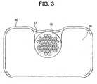
- the end result is represented in the schematic cross-section shown in Figure 3 , where the Formvar® layer 30 coats the superconducting multifilamentary wire 10, copper channel 20, and the high temperature solder 21.
- a solder alloy Sn-5wt%Sb having a melting temperature range of 232-240°C was used to solder a copper-matrix (copper alloy UNS 10100) superconductor wire consisting of 31 filaments of Nb-47wt%Ti into a copper channel at 260°C.
- This soldered composite was cleaned and then coated with Formvar® and passed through a tower furnace operating at 400°C. The wire temperature measured at the exit of the tower was 205°C. The coating and curing steps were repeated several times to build an acceptable layer of Formvar® on the composite surface. The resulting product had excellent properties.
Landscapes
- Engineering & Computer Science (AREA)
- Manufacturing & Machinery (AREA)
- Superconductors And Manufacturing Methods Therefor (AREA)
Claims (16)
- Procédé de fabrication d'un fil composite supraconducteur multifilament soudé par brasure isolé, comprenant les étapes consistant à :(a) créer un fil composite non isolé en utilisant une brasure à point de fusion élevé comprenant principalement du Sn avec un ou plusieurs métaux d'alliage choisis dans le groupe constitué par Sb, Ag et Cu, et souder par brasure un composite supraconducteur multifilament à un composant métallique soudable ;(b) appliquer un revêtement de film d'isolation polymère sur le fil composite de l'étape (a) ; et(c) soumettre l'ensemble de l'étape (b) à un chauffage dans un four à des températures de four et sur une période suffisantes pour durcir ladite isolation, mais insuffisantes pour faire fondre ladite brasure.
- Procédé selon la revendication 1, dans lequel le point de fusion de la brasure est supérieur à 200 °C et inférieur à 300 °C.
- Procédé selon la revendication 2, dans lequel la brasure à point de fusion élevé est du Sn à 5 % de Sb.
- Procédé selon la revendication 1, dans lequel le composite multifilament comprend des filaments d'alliage Nb-Ti dans une matrice de cuivre, ou des filaments d'alliage Nb-Ti dans une matrice d'alliage Cu-Ni.
- Procédé selon la revendication 1, dans lequel le composite supraconducteur multifilament a une section transversale ronde, ou une section transversale généralement rectangulaire.
- Procédé selon la revendication 5, dans lequel le composite supraconducteur multifilament a une section transversale ronde et dans lequel le composite soudé est fabriqué en enroulant une bande de Cu autour d'un fil rond.
- Procédé selon la revendication 5, dans lequel le composite supraconducteur multifilament a une section transversale ronde et dans lequel le composite soudé est fabriqué par le « procédé du fil en canal » de soudage d'un fil rond dans un sillon rond dans un canal de forme généralement rectangulaire.
- Procédé selon la revendication 7 dans lequel le canal métallique soudable est du Cu pur, un alliage de Cu, ou un métal plaqué de Cu.
- Procédé selon la revendication 5, dans lequel le composite supraconducteur multifilament a une section transversale généralement rectangulaire, et dans lequel le composite soudé est fabriqué en soudant un fil rectangulaire (plat) à une bande rectangulaire de Cu, d'alliage de Cu, ou d'un métal plaqué de Cu.
- Procédé selon la revendication 1 dans lequel le revêtement polymère est une isolation par vernis Formvar® (résine de polyvinylacétal modifiée).
- Procédé selon la revendication 1 dans lequel le revêtement polymère est choisi dans le groupe constitué par les isolations de type époxyde, émail, nylon ou vernis avec une température de durcissement de plus de 300 °C.
- Procédé selon la revendication 1, où après application de l'isolation, le composite entier est étiré et/ou façonné dans une configuration souhaitée.
- Procédé selon la revendication 1 dans lequel l'application de l'isolation polymère se fait par extrusion.
- Procédé selon la revendication 13, dans lequel le polymère utilisé est un polymère extrudable choisi dans le groupe constitué par le nylon, l'époxyde, le PVC, le polyéthylène et les polymères chlorofluorocarbonés.
- Procédé selon la revendication 1, dans lequel la brasure de surface, mais pas la soudure par brasure du fil au canal, est retirée avant application de l'isolation par retrait électrolytique de la brasure.
- Procédé selon la revendication 1, dans lequel la brasure de surface est rendue rugueuse par sablage, grenaillage, ou gaufrage.
Applications Claiming Priority (2)
| Application Number | Priority Date | Filing Date | Title |
|---|---|---|---|
| US11/651,443 US20080163474A1 (en) | 2007-01-09 | 2007-01-09 | Soldered superconductor with hard insulation |
| PCT/US2008/000229 WO2008085955A2 (fr) | 2007-01-09 | 2008-01-08 | Supraconducteur soudé avec isolation rigide |
Publications (3)
| Publication Number | Publication Date |
|---|---|
| EP2118941A2 EP2118941A2 (fr) | 2009-11-18 |
| EP2118941A4 EP2118941A4 (fr) | 2013-05-29 |
| EP2118941B1 true EP2118941B1 (fr) | 2014-08-13 |
Family
ID=39593028
Family Applications (1)
| Application Number | Title | Priority Date | Filing Date |
|---|---|---|---|
| EP08724435.6A Active EP2118941B1 (fr) | 2007-01-09 | 2008-01-08 | Supraconducteur soudé avec isolation rigide |
Country Status (3)
| Country | Link |
|---|---|
| US (1) | US20080163474A1 (fr) |
| EP (1) | EP2118941B1 (fr) |
| WO (1) | WO2008085955A2 (fr) |
Cited By (2)
| Publication number | Priority date | Publication date | Assignee | Title |
|---|---|---|---|---|
| WO2019177026A1 (fr) | 2018-03-14 | 2019-09-19 | 三菱マテリアル株式会社 | Procédé de fabrication de matériau de fil conducteur isolé |
| WO2019188654A1 (fr) | 2018-03-26 | 2019-10-03 | 三菱マテリアル株式会社 | Procédé permettant de fabriquer une tige de fil supraconducteur isolante |
Families Citing this family (7)
| Publication number | Priority date | Publication date | Assignee | Title |
|---|---|---|---|---|
| DE102012218250A1 (de) * | 2012-10-05 | 2014-04-10 | Bruker Eas Gmbh | Verfahren zur Fertigung eines Supraleiterdrahts, insbesondere unter Verwendung bleifreier Lote |
| US10573435B2 (en) * | 2016-01-29 | 2020-02-25 | Bruker Ost Llc | Method for producing a multifilament Nb3Sn superconducting wire |
| US11075435B2 (en) | 2018-10-25 | 2021-07-27 | International Business Machines Corporation | Electroplating of niobium titanium |
| CN113950725B (zh) * | 2019-05-31 | 2026-01-27 | 古河电气工业株式会社 | 树脂被覆超导线、超导线圈及屏蔽线圈 |
| CN110767376B (zh) * | 2019-11-14 | 2020-12-08 | 中国科学院合肥物质科学研究院 | 一种适用于提高高温超导复合化导体力学性能的热成型方法 |
| US11735802B2 (en) | 2020-04-27 | 2023-08-22 | International Business Machines Corporation | Electroplated metal layer on a niobium-titanium substrate |
| CN111599530B (zh) * | 2020-05-15 | 2021-08-03 | 西部超导材料科技股份有限公司 | 获取超导线材铜槽线加工率的方法 |
Family Cites Families (11)
| Publication number | Priority date | Publication date | Assignee | Title |
|---|---|---|---|---|
| US3951870A (en) * | 1973-09-13 | 1976-04-20 | The Carborundum Company | Superconductive transition metal carbonitride fibers and method for the preparation thereof |
| US4278310A (en) * | 1978-04-04 | 1981-07-14 | Gte Products Corporation | Method of making a percussively-ignited photoflash lamp |
| US4480007A (en) * | 1980-09-03 | 1984-10-30 | General Electric Company | Enamel having improved coatability and insulated electrical articles produced therefrom |
| US4506109A (en) * | 1981-05-28 | 1985-03-19 | Agency Of Ind. Science And Technology | Al-stabilized superconducting wire and the method for producing the same |
| JPS60250834A (ja) * | 1984-05-25 | 1985-12-11 | Hitachi Cable Ltd | エナメル絶縁被覆銅安定化超電導線材の製造法 |
| US4980964A (en) * | 1988-08-19 | 1991-01-01 | Jan Boeke | Superconducting wire |
| US4959279A (en) * | 1989-01-17 | 1990-09-25 | The Furukawa Electric Co., Ltd. | Superconducting wire containing multifilamentary superconducting alloy |
| JPH04106809A (ja) * | 1990-08-24 | 1992-04-08 | Furukawa Electric Co Ltd:The | 超電導導体 |
| SE9802386D0 (sv) * | 1998-07-03 | 1998-07-03 | Borealis As | Composition for elektric cables |
| US6932874B2 (en) * | 2002-11-01 | 2005-08-23 | Oxford Superconducting Technology | Method for increasing the copper to superconductor ratio in a superconductor wire |
| US7089647B2 (en) * | 2003-02-21 | 2006-08-15 | Oxford Superconducting Technology | Increasing the copper to superconductor ratio of a superconductor wire by cladding with copper-based strip |
-
2007
- 2007-01-09 US US11/651,443 patent/US20080163474A1/en not_active Abandoned
-
2008
- 2008-01-08 EP EP08724435.6A patent/EP2118941B1/fr active Active
- 2008-01-08 WO PCT/US2008/000229 patent/WO2008085955A2/fr not_active Ceased
Cited By (2)
| Publication number | Priority date | Publication date | Assignee | Title |
|---|---|---|---|---|
| WO2019177026A1 (fr) | 2018-03-14 | 2019-09-19 | 三菱マテリアル株式会社 | Procédé de fabrication de matériau de fil conducteur isolé |
| WO2019188654A1 (fr) | 2018-03-26 | 2019-10-03 | 三菱マテリアル株式会社 | Procédé permettant de fabriquer une tige de fil supraconducteur isolante |
Also Published As
| Publication number | Publication date |
|---|---|
| WO2008085955A2 (fr) | 2008-07-17 |
| EP2118941A4 (fr) | 2013-05-29 |
| US20080163474A1 (en) | 2008-07-10 |
| WO2008085955A3 (fr) | 2008-08-28 |
| EP2118941A2 (fr) | 2009-11-18 |
Similar Documents
| Publication | Publication Date | Title |
|---|---|---|
| EP2118941B1 (fr) | Supraconducteur soudé avec isolation rigide | |
| CN101356660B (zh) | 线在沟道内超导体及其制造方法 | |
| US3983521A (en) | Flexible superconducting composite compound wires | |
| US6444917B1 (en) | Encapsulated ceramic superconductors | |
| KR100547458B1 (ko) | 전자부품용리드재,그것을이용한리드및반도체장치 | |
| CN100422361C (zh) | 制造粉末冶金工艺Nb3Sn超导线的方法、粉末冶金工艺Nb3Sn超导线前体 | |
| JP5841862B2 (ja) | 高温超電導線材および高温超電導コイル | |
| US4161062A (en) | Method for producing hollow superconducting cables | |
| US20090312187A1 (en) | Method for fabricating a superconducting wire | |
| EP1981039B1 (fr) | Procédé de fabrication d'un supraconducteur composite | |
| USRE32178E (en) | Process for producing compound based superconductor wire | |
| JP4936525B2 (ja) | 複合超電導体 | |
| JP2021061135A (ja) | 酸化物超電導線材、超電導コイルおよび超電導コイルの製造方法 | |
| JP2009170257A (ja) | 超電導テープおよび超電導テープの製造方法 | |
| JP3944573B2 (ja) | Nb3Al超伝導線材の製造方法とその方法により得られるNb3Al超伝導線材 | |
| WO2008015941A1 (fr) | Fil supraconducteur composite, procédé de fabrication associé, et câble supraconducteur | |
| US20040209779A1 (en) | Method for increasing the copper to superconductor ratio in a superconductor wire | |
| US6845254B2 (en) | Nb3Ga multifilamentary superconducting wire and process for preparing the same | |
| WO2017104297A1 (fr) | Procédé de production de fil supraconducteur oxyde, et procédé de production de bobine supraconductrice | |
| JPH11353961A (ja) | Nb3Sn化合物超電導体の前駆線材およびその製造方法、Nb3Sn化合物超電導導体の製造方法、並びにNb3Sn化合物超電導コイルの製造方法 | |
| JP3753346B2 (ja) | アルミニウム安定化超電導線 | |
| JP2009170221A (ja) | 超電導テープの製造方法および超電導テープの製造装置 | |
| JP3428771B2 (ja) | Nb3Sn系化合物超電導線材 | |
| JPH04106809A (ja) | 超電導導体 | |
| JPH0645141A (ja) | 酸化物超電導体電流リードの電極 |
Legal Events
| Date | Code | Title | Description |
|---|---|---|---|
| PUAI | Public reference made under article 153(3) epc to a published international application that has entered the european phase |
Free format text: ORIGINAL CODE: 0009012 |
|
| 17P | Request for examination filed |
Effective date: 20090807 |
|
| AK | Designated contracting states |
Kind code of ref document: A2 Designated state(s): AT BE BG CH CY CZ DE DK EE ES FI FR GB GR HR HU IE IS IT LI LT LU LV MC MT NL NO PL PT RO SE SI SK TR |
|
| DAX | Request for extension of the european patent (deleted) | ||
| A4 | Supplementary search report drawn up and despatched |
Effective date: 20130502 |
|
| RIC1 | Information provided on ipc code assigned before grant |
Ipc: H01L 39/24 20060101AFI20130424BHEP |
|
| GRAP | Despatch of communication of intention to grant a patent |
Free format text: ORIGINAL CODE: EPIDOSNIGR1 |
|
| INTG | Intention to grant announced |
Effective date: 20140224 |
|
| GRAS | Grant fee paid |
Free format text: ORIGINAL CODE: EPIDOSNIGR3 |
|
| GRAA | (expected) grant |
Free format text: ORIGINAL CODE: 0009210 |
|
| AK | Designated contracting states |
Kind code of ref document: B1 Designated state(s): AT BE BG CH CY CZ DE DK EE ES FI FR GB GR HR HU IE IS IT LI LT LU LV MC MT NL NO PL PT RO SE SI SK TR |
|
| REG | Reference to a national code |
Ref country code: GB Ref legal event code: FG4D |
|
| REG | Reference to a national code |
Ref country code: AT Ref legal event code: REF Ref document number: 682664 Country of ref document: AT Kind code of ref document: T Effective date: 20140815 Ref country code: CH Ref legal event code: EP |
|
| REG | Reference to a national code |
Ref country code: IE Ref legal event code: FG4D |
|
| REG | Reference to a national code |
Ref country code: DE Ref legal event code: R096 Ref document number: 602008033821 Country of ref document: DE Effective date: 20140925 |
|
| REG | Reference to a national code |
Ref country code: CH Ref legal event code: NV Representative=s name: E. BLUM AND CO. AG PATENT- UND MARKENANWAELTE , CH |
|
| REG | Reference to a national code |
Ref country code: NL Ref legal event code: VDEP Effective date: 20140813 |
|
| REG | Reference to a national code |
Ref country code: AT Ref legal event code: MK05 Ref document number: 682664 Country of ref document: AT Kind code of ref document: T Effective date: 20140813 |
|
| REG | Reference to a national code |
Ref country code: LT Ref legal event code: MG4D |
|
| PG25 | Lapsed in a contracting state [announced via postgrant information from national office to epo] |
Ref country code: NO Free format text: LAPSE BECAUSE OF FAILURE TO SUBMIT A TRANSLATION OF THE DESCRIPTION OR TO PAY THE FEE WITHIN THE PRESCRIBED TIME-LIMIT Effective date: 20141113 Ref country code: SE Free format text: LAPSE BECAUSE OF FAILURE TO SUBMIT A TRANSLATION OF THE DESCRIPTION OR TO PAY THE FEE WITHIN THE PRESCRIBED TIME-LIMIT Effective date: 20140813 Ref country code: ES Free format text: LAPSE BECAUSE OF FAILURE TO SUBMIT A TRANSLATION OF THE DESCRIPTION OR TO PAY THE FEE WITHIN THE PRESCRIBED TIME-LIMIT Effective date: 20140813 Ref country code: BG Free format text: LAPSE BECAUSE OF FAILURE TO SUBMIT A TRANSLATION OF THE DESCRIPTION OR TO PAY THE FEE WITHIN THE PRESCRIBED TIME-LIMIT Effective date: 20141113 Ref country code: GR Free format text: LAPSE BECAUSE OF FAILURE TO SUBMIT A TRANSLATION OF THE DESCRIPTION OR TO PAY THE FEE WITHIN THE PRESCRIBED TIME-LIMIT Effective date: 20141114 Ref country code: LT Free format text: LAPSE BECAUSE OF FAILURE TO SUBMIT A TRANSLATION OF THE DESCRIPTION OR TO PAY THE FEE WITHIN THE PRESCRIBED TIME-LIMIT Effective date: 20140813 Ref country code: PT Free format text: LAPSE BECAUSE OF FAILURE TO SUBMIT A TRANSLATION OF THE DESCRIPTION OR TO PAY THE FEE WITHIN THE PRESCRIBED TIME-LIMIT Effective date: 20141215 |
|
| PG25 | Lapsed in a contracting state [announced via postgrant information from national office to epo] |
Ref country code: AT Free format text: LAPSE BECAUSE OF FAILURE TO SUBMIT A TRANSLATION OF THE DESCRIPTION OR TO PAY THE FEE WITHIN THE PRESCRIBED TIME-LIMIT Effective date: 20140813 Ref country code: IS Free format text: LAPSE BECAUSE OF FAILURE TO SUBMIT A TRANSLATION OF THE DESCRIPTION OR TO PAY THE FEE WITHIN THE PRESCRIBED TIME-LIMIT Effective date: 20141213 Ref country code: HR Free format text: LAPSE BECAUSE OF FAILURE TO SUBMIT A TRANSLATION OF THE DESCRIPTION OR TO PAY THE FEE WITHIN THE PRESCRIBED TIME-LIMIT Effective date: 20140813 Ref country code: LV Free format text: LAPSE BECAUSE OF FAILURE TO SUBMIT A TRANSLATION OF THE DESCRIPTION OR TO PAY THE FEE WITHIN THE PRESCRIBED TIME-LIMIT Effective date: 20140813 Ref country code: CY Free format text: LAPSE BECAUSE OF FAILURE TO SUBMIT A TRANSLATION OF THE DESCRIPTION OR TO PAY THE FEE WITHIN THE PRESCRIBED TIME-LIMIT Effective date: 20140813 |
|
| PG25 | Lapsed in a contracting state [announced via postgrant information from national office to epo] |
Ref country code: NL Free format text: LAPSE BECAUSE OF FAILURE TO SUBMIT A TRANSLATION OF THE DESCRIPTION OR TO PAY THE FEE WITHIN THE PRESCRIBED TIME-LIMIT Effective date: 20140813 |
|
| PG25 | Lapsed in a contracting state [announced via postgrant information from national office to epo] |
Ref country code: SK Free format text: LAPSE BECAUSE OF FAILURE TO SUBMIT A TRANSLATION OF THE DESCRIPTION OR TO PAY THE FEE WITHIN THE PRESCRIBED TIME-LIMIT Effective date: 20140813 Ref country code: RO Free format text: LAPSE BECAUSE OF FAILURE TO SUBMIT A TRANSLATION OF THE DESCRIPTION OR TO PAY THE FEE WITHIN THE PRESCRIBED TIME-LIMIT Effective date: 20140813 Ref country code: DK Free format text: LAPSE BECAUSE OF FAILURE TO SUBMIT A TRANSLATION OF THE DESCRIPTION OR TO PAY THE FEE WITHIN THE PRESCRIBED TIME-LIMIT Effective date: 20140813 Ref country code: CZ Free format text: LAPSE BECAUSE OF FAILURE TO SUBMIT A TRANSLATION OF THE DESCRIPTION OR TO PAY THE FEE WITHIN THE PRESCRIBED TIME-LIMIT Effective date: 20140813 Ref country code: EE Free format text: LAPSE BECAUSE OF FAILURE TO SUBMIT A TRANSLATION OF THE DESCRIPTION OR TO PAY THE FEE WITHIN THE PRESCRIBED TIME-LIMIT Effective date: 20140813 |
|
| REG | Reference to a national code |
Ref country code: DE Ref legal event code: R097 Ref document number: 602008033821 Country of ref document: DE |
|
| PG25 | Lapsed in a contracting state [announced via postgrant information from national office to epo] |
Ref country code: PL Free format text: LAPSE BECAUSE OF FAILURE TO SUBMIT A TRANSLATION OF THE DESCRIPTION OR TO PAY THE FEE WITHIN THE PRESCRIBED TIME-LIMIT Effective date: 20140813 |
|
| PLBE | No opposition filed within time limit |
Free format text: ORIGINAL CODE: 0009261 |
|
| STAA | Information on the status of an ep patent application or granted ep patent |
Free format text: STATUS: NO OPPOSITION FILED WITHIN TIME LIMIT |
|
| PG25 | Lapsed in a contracting state [announced via postgrant information from national office to epo] |
Ref country code: BE Free format text: LAPSE BECAUSE OF NON-PAYMENT OF DUE FEES Effective date: 20150131 |
|
| 26N | No opposition filed |
Effective date: 20150515 |
|
| PG25 | Lapsed in a contracting state [announced via postgrant information from national office to epo] |
Ref country code: LU Free format text: LAPSE BECAUSE OF FAILURE TO SUBMIT A TRANSLATION OF THE DESCRIPTION OR TO PAY THE FEE WITHIN THE PRESCRIBED TIME-LIMIT Effective date: 20150108 |
|
| PG25 | Lapsed in a contracting state [announced via postgrant information from national office to epo] |
Ref country code: MC Free format text: LAPSE BECAUSE OF FAILURE TO SUBMIT A TRANSLATION OF THE DESCRIPTION OR TO PAY THE FEE WITHIN THE PRESCRIBED TIME-LIMIT Effective date: 20140813 |
|
| REG | Reference to a national code |
Ref country code: FR Ref legal event code: ST Effective date: 20150930 |
|
| REG | Reference to a national code |
Ref country code: IE Ref legal event code: MM4A |
|
| PG25 | Lapsed in a contracting state [announced via postgrant information from national office to epo] |
Ref country code: SI Free format text: LAPSE BECAUSE OF FAILURE TO SUBMIT A TRANSLATION OF THE DESCRIPTION OR TO PAY THE FEE WITHIN THE PRESCRIBED TIME-LIMIT Effective date: 20140813 Ref country code: FR Free format text: LAPSE BECAUSE OF NON-PAYMENT OF DUE FEES Effective date: 20150202 |
|
| PG25 | Lapsed in a contracting state [announced via postgrant information from national office to epo] |
Ref country code: IE Free format text: LAPSE BECAUSE OF NON-PAYMENT OF DUE FEES Effective date: 20150108 |
|
| PG25 | Lapsed in a contracting state [announced via postgrant information from national office to epo] |
Ref country code: BE Free format text: LAPSE BECAUSE OF FAILURE TO SUBMIT A TRANSLATION OF THE DESCRIPTION OR TO PAY THE FEE WITHIN THE PRESCRIBED TIME-LIMIT Effective date: 20140813 |
|
| PG25 | Lapsed in a contracting state [announced via postgrant information from national office to epo] |
Ref country code: MT Free format text: LAPSE BECAUSE OF FAILURE TO SUBMIT A TRANSLATION OF THE DESCRIPTION OR TO PAY THE FEE WITHIN THE PRESCRIBED TIME-LIMIT Effective date: 20140813 |
|
| PG25 | Lapsed in a contracting state [announced via postgrant information from national office to epo] |
Ref country code: HU Free format text: LAPSE BECAUSE OF FAILURE TO SUBMIT A TRANSLATION OF THE DESCRIPTION OR TO PAY THE FEE WITHIN THE PRESCRIBED TIME-LIMIT; INVALID AB INITIO Effective date: 20080108 |
|
| PG25 | Lapsed in a contracting state [announced via postgrant information from national office to epo] |
Ref country code: TR Free format text: LAPSE BECAUSE OF FAILURE TO SUBMIT A TRANSLATION OF THE DESCRIPTION OR TO PAY THE FEE WITHIN THE PRESCRIBED TIME-LIMIT Effective date: 20140813 |
|
| REG | Reference to a national code |
Ref country code: DE Ref legal event code: R079 Ref document number: 602008033821 Country of ref document: DE Free format text: PREVIOUS MAIN CLASS: H01L0039240000 Ipc: H10N0060010000 |
|
| P01 | Opt-out of the competence of the unified patent court (upc) registered |
Effective date: 20231205 |
|
| REG | Reference to a national code |
Ref country code: CH Ref legal event code: U11 Free format text: ST27 STATUS EVENT CODE: U-0-0-U10-U11 (AS PROVIDED BY THE NATIONAL OFFICE) Effective date: 20260201 |
|
| PGFP | Annual fee paid to national office [announced via postgrant information from national office to epo] |
Ref country code: GB Payment date: 20260122 Year of fee payment: 19 |
|
| PGFP | Annual fee paid to national office [announced via postgrant information from national office to epo] |
Ref country code: DE Payment date: 20260120 Year of fee payment: 19 |
|
| PGFP | Annual fee paid to national office [announced via postgrant information from national office to epo] |
Ref country code: FI Payment date: 20260120 Year of fee payment: 19 Ref country code: IT Payment date: 20260130 Year of fee payment: 19 |
|
| PGFP | Annual fee paid to national office [announced via postgrant information from national office to epo] |
Ref country code: CH Payment date: 20260201 Year of fee payment: 19 |