EP2118919B1 - Apparatus and method for reducing edge effect in an image sensor - Google Patents
Apparatus and method for reducing edge effect in an image sensor Download PDFInfo
- Publication number
- EP2118919B1 EP2118919B1 EP08725835.6A EP08725835A EP2118919B1 EP 2118919 B1 EP2118919 B1 EP 2118919B1 EP 08725835 A EP08725835 A EP 08725835A EP 2118919 B1 EP2118919 B1 EP 2118919B1
- Authority
- EP
- European Patent Office
- Prior art keywords
- pixels
- pixel
- dummy
- clear
- dummy pixel
- Prior art date
- Legal status (The legal status is an assumption and is not a legal conclusion. Google has not performed a legal analysis and makes no representation as to the accuracy of the status listed.)
- Active
Links
Images


Classifications
-
- H—ELECTRICITY
- H10—SEMICONDUCTOR DEVICES; ELECTRIC SOLID-STATE DEVICES NOT OTHERWISE PROVIDED FOR
- H10F—INORGANIC SEMICONDUCTOR DEVICES SENSITIVE TO INFRARED RADIATION, LIGHT, ELECTROMAGNETIC RADIATION OF SHORTER WAVELENGTH OR CORPUSCULAR RADIATION
- H10F39/00—Integrated devices, or assemblies of multiple devices, comprising at least one element covered by group H10F30/00, e.g. radiation detectors comprising photodiode arrays
- H10F39/10—Integrated devices
- H10F39/12—Image sensors
- H10F39/18—Complementary metal-oxide-semiconductor [CMOS] image sensors; Photodiode array image sensors
-
- H—ELECTRICITY
- H04—ELECTRIC COMMUNICATION TECHNIQUE
- H04N—PICTORIAL COMMUNICATION, e.g. TELEVISION
- H04N25/00—Circuitry of solid-state image sensors [SSIS]; Control thereof
- H04N25/60—Noise processing, e.g. detecting, correcting, reducing or removing noise
- H04N25/63—Noise processing, e.g. detecting, correcting, reducing or removing noise applied to dark current
- H04N25/633—Noise processing, e.g. detecting, correcting, reducing or removing noise applied to dark current by using optical black pixels
-
- H—ELECTRICITY
- H10—SEMICONDUCTOR DEVICES; ELECTRIC SOLID-STATE DEVICES NOT OTHERWISE PROVIDED FOR
- H10F—INORGANIC SEMICONDUCTOR DEVICES SENSITIVE TO INFRARED RADIATION, LIGHT, ELECTROMAGNETIC RADIATION OF SHORTER WAVELENGTH OR CORPUSCULAR RADIATION
- H10F39/00—Integrated devices, or assemblies of multiple devices, comprising at least one element covered by group H10F30/00, e.g. radiation detectors comprising photodiode arrays
- H10F39/80—Constructional details of image sensors
- H10F39/803—Pixels having integrated switching, control, storage or amplification elements
-
- H—ELECTRICITY
- H10—SEMICONDUCTOR DEVICES; ELECTRIC SOLID-STATE DEVICES NOT OTHERWISE PROVIDED FOR
- H10F—INORGANIC SEMICONDUCTOR DEVICES SENSITIVE TO INFRARED RADIATION, LIGHT, ELECTROMAGNETIC RADIATION OF SHORTER WAVELENGTH OR CORPUSCULAR RADIATION
- H10F39/00—Integrated devices, or assemblies of multiple devices, comprising at least one element covered by group H10F30/00, e.g. radiation detectors comprising photodiode arrays
- H10F39/80—Constructional details of image sensors
- H10F39/802—Geometry or disposition of elements in pixels, e.g. address-lines or gate electrodes
Definitions
- the present invention relates generally to image processing for electronic imaging sensors, and more particularly, to an apparatus and method for equalizing the dark current in pixels located on the periphery of an image sensor and thereby eliminating the so-called "edge effect" to optimize image quality.
- OB pixels are the reference pixels within an imaging sensor pixel array that should have virtually identical electrical characteristics as a standard active pixel, yet are insensitive to light.
- OB pixels are used by various image processing circuits in the sensor or camera to maintain a constant black level independent of gain, illumination, changes in sensor operating conditions, etc.
- An OB pixel's signal is normally processed using the same signal chain and timing as those that are photo-electrically responsive and form the image of interest.
- the latter pixels, which constitute the majority of pixels in an imaging sensor are some times referred to as "Clear Pixels.” While clear pixels form the actual image, OB pixels are indirectly used in the image formation process. Instead, OB pixels are used to track the environmental and operational status of the imaging sensor while also providing information regarding dark signal/current, column noise and line noise at the specific location of each OB pixel.
- OB pixels are typically used as reference pixels for many calibration operations that enhance image quality. These include black clamp stabilization, flutter rejection, column noise suppression and line noise correction. In these and other algorithms, OB pixels must have similar dark signal response as a clear pixel; they must mimic the response that a clear pixel would normally have in the absence light to accurately establish the current vs. voltage (i-v) characteristic for general reference in the image sensor.
- i-v current vs. voltage
- I I o e / nkT q V d ⁇ 1
- I I o e / nkT q V d ⁇ 1
- I o the diode's saturation current
- V d the diode voltage
- n the diode ideality
- k Boltzman's constant
- T the Temperature.
- the saturation current can vary significantly from diode to diode.
- n d is the diode ideality for the specific diode
- the parameter R o A is its resistance-area product at zero volts of applied bias, expressed in units of ohm-cm 2 . While diode resistance and saturation current depend on area, the R o A product for a specific technology is independent of area and characterizes the quality of diode fabrication.
- CMOS sensor used in a studio broadcast camera to generate content for HDTV production requires significantly higher image quality than a CMOS sensor used in consumer camcorders (medium to low-end product application).
- CMOS sensor used in consumer camcorders medium to low-end product application.
- other quality factors include drift-free operation and insensitivity to excess illumination. Maximizing image quality hence entails not only better clear pixel quality, but also better OB quality. Consequently, a critical property of an OB pixel (active or dummy) is how closely it truly represents the dark signal response of a clear pixel regardless of incident lighting and environment including physical and electrical stress.
- high end applications require an OB pixel to have significantly higher fidelity under extreme conditions, e.g., superior opacity, thermal stability, and well-behaved electrical characteristics including detector ideality, n d , and R o A product.
- the total current accumulated in clear pixels versus that in OB pixels should differ only by the clear pixel photocurrent, I photo ; I photo must be zero in OB and OB dummy pixels.
- dummy pixels are disclosed that exhibit identical electrical characteristics to any other pixel in the imaging array. This insures that the total current of each dummy pixel used in an array also containing clear pixels and OB pixels is roughly identical to the total current of a clear pixel. While an OB pixel used as a reference for signal processing is read each frame, a dummy pixel must look the same even though it may never be read, regardless whether it is opaque or light-sensitive. Further, the dummy pixels do not perturb the electrical characteristics of nearby pixels so that they can be used to isolate the various sub-arrays that compose an imaging array. Such dummy pixels are also placed at the edges of the imaging array to prevent discontinuities stemming from process-related, physical and electrical factors. Edge effects are thereby eliminated.
- the preferred embodiment of the dummy pixel is a clear type with identical electrical characteristics to the clear pixels in the main imaging array.
- a second embodiment of the dummy pixel is optically black to support optional signal processing functions.
- Dummy OB pixels are constituted in the present invention by:
- dummy OB pixel formation is completed by operating the dummy pixels with the reset transistor biased in soft reset mode to prevent signal integration. This insures low-noise operation and minimizes generation of excess generation-recombination currents that alter diode ideality and/or R o A product.
- Dummy clear pixel formation is completed by omitting step 1 and again operating these pixels with the reset transistor biased in soft reset mode.
- Dummy clear pixels are the main guard bands protecting the imaging array from deleterious edge effects since the omission of the OB step results in the best possible electrical match to the clear pixels in the imaging array.
- the present invention provides a dummy pixel, an image sensor and a method of reducing dark current in an image sensor as recited in claims 1, 9 and 11, respectively.
- a dummy pixel may comprise a photodiode and a reset transistor connected to the photodiode, wherein the reset transistor is biased in a soft reset mode.
- a method of the present invention may comprise forming at least one row or column of dummy pixels in an image sensor, wherein each dummy pixel comprises a pixel having a reset transistor permanently biased in a soft reset mode.
- An image sensor formed according to the present invention may comprise an array of clear pixels, a plurality of sub-arrays of optical black pixels, and a plurality of sub-arrays of dummy pixels located between the array of clear pixels and the sub-arrays of optical black pixels, wherein each dummy pixel comprises a photodiode, and a reset transistor connected to the photodiode, wherein the reset transistor is biased in a soft reset mode.
- a dummy pixel may be formed as either a clear pixel or an optical black pixel.
- the present invention provides clear dummy pixels and Optical Black (OB) dummy pixels having virtually identical electrical characteristics as the clear pixels in the imaging sensor.
- the dummy pixels are not necessarily read out but form isolation regions within the array that do not create regional discontinuities resulting in edge effects.
- the dummy pixels are free of the impediments of existing techniques that complicate sensor design and production. Specifically, the Shockley currents generated in the dummy pixels of the various embodiments are approximately identical to the Shockley current of clear pixels. Furthermore, since there is effectively zero photocurrent generated in the dummy OB pixel, the specific photocurrent generated in each clear pixel represents the net signal relative to the black level.
- Existing techniques generally require significant changes to process technologies and these deviations are incompatible with standard wafer production.
- the present invention minimizes dispersion in the key photodetector characteristics n d and R o A in order to maximize imaging array uniformity (by minimizing edge effects) and to thereby maximize image quality produced by the imaging sensor.
- the idealities and R o A products for clear and OB pixels should be roughly identical and consistent with the generic diode formation technology regardless of the pixel's location and function.
- dummy pixels are clear pixels which do not have to be read out, but are biased in an alternative configuration that enables attainment of intrinsic performance regardless of pixel location.
- the clear dummy pixels are used to isolate regions of clear active pixels from OB pixels without inducing edge effects.
- OB dummy pixels are alternately used for isolation and signal processing operations.
- fabrication of dummy pixels is effectively partitioned into two principal areas: 1) electrical performance and 2) optical performance.
- image sensor electrical performance is unaffected by the additional processing needed to optimally form OB pixels, apply color filters, form microlenses, apply a protecting layer over the sensor surface, and actually operate the various pixels.
- the thickness of the metal mask used for OB formation to render the OB pixel opaque can be adjusted to increase opacity and decrease light transmission into the OB pixel, but is typically on the order of 1000 ⁇ when applied via standard sputtering means.
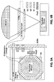
- Fig. 5A shows a top layer view of the pixel layout including the location of the Ti/TiN pad over the photodiode and under the microlens.
- Fig. 5B is a cross-section plan showing how the Ti/TiN metallization blocks light focused by the microlens, yet allows the photodiode diffusion to be accessible to annealing ions during the final processing steps.
- the optical black pixel structure of Fig. 5 is further described in related U.S. Patent Application No. TBD, entitled APPARATUS AND METHOD FOR FORMING OPTICAL BLACK PIXELS WITH UNIFORMLY LOW DARK CURRENT.
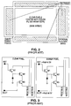
- the pixel array of U.S. Serial No. 11/461,457 is segmented into isolated sub-array blocks, as illustrated in Fig. 2 .
- the primary blocks include:
- the clear dummy sub-arrays of Fig. 2 interconnect throughout the array and generally fill the physical space between the clear pixel array and the OB sub-arrays. Dummy arrays are also placed at the very edge of the array except when an optional n- guard band is used.
- the latter guard band is typically about 40 to 60 pixels wide, assuming pixel spacing of about 2 ⁇ m, as a collecting guard band of at least 100 ⁇ m width is needed to capture stray minority carriers that may be self-photogenerated or have been scattered or migrated from the clear pixel array or the peripheral circuits surrounding the entire pixel array.
- Fig. 2 shows an N- guard band located on the right side as it is assumed here that light-emitting digital circuits are present to the right of the pixel array.
- the N-guard band is composed of a series of diffusions formed with the same sensor implant and diffusion area as the clear pixels to also prevent creation of edge effects while forming an effective sink for stray minority carriers.
- each dummy pixel photodiode was kept at 0V potential by physically connecting the Select signal (SLCT) to the photodiode diffusion and imposing the condition, for dummy pixels, that the SLCT signal be held at 0V.
- SLCT Select signal
- Such a bias condition corresponds to full well saturation and is therefore largely unfavorable for attracting large numbers of minority carriers in the typical p-type substrate (electron). Consequently, while this type guard band can capture a few stray photo-generated signals from the underlying bulk, it can not minimize dark current accumulation in the neighboring pixels.
- holding dummy pixels at 0V resulted in excess generation-recombination current compared to active pixels.
- Pixels located at the periphery of the pixel array in imaging sensors typically show an anomalous behavior that is often referred to as edge effect.
- edge effect For example, pixel dark current is often higher along the sensor perimeter.
- pixels belonging to, or in proximity of, the pixel array edges normally can not be used as imaging or OB pixels.
- a certain number of clear pixels can be used as a buffering region.
- this approach results in a wasted silicon real estate and ultimately in higher product cost.
- dummy pixel Significant improvement in minimizing edge effects in the horizontal direction is achieved by using an improved type of dummy pixel.
- a key point is to devise the dummy pixel configuration so that it helps stabilize the local environment while deflecting minority carriers away from the edges of the pixel array and operating at a quiescent bias that best mimics clear pixels.
- Another key point is that the dummy pixel is not encumbered with optical black to further insure that its properties are virtually identical to those of clear pixels in the imaging array.
- the present invention includes a preferred embodiment of this isolation strategy.
- the dummy pixel consists of a clear pixel that is configured with the reset transistor biased in soft reset mode.
- the reset transistor biased in soft reset mode.
- a photodiode dynamically pulls minority carriers that are within one diffusion length toward this higher potential (Vaa-Vth; i.e., one threshold voltage below the analog supply voltage) rather than letting them drift in the substrate.
- Vaa-Vth i.e., one threshold voltage below the analog supply voltage
- the associated junctions collect the stray electrons (minority carriers) rather than letting them continue to drift and scatter through the substrate.
- the dummy photodiode of the preferred embodiment thus acts a sink for any stray electrons within a diffusion length of the junction. Consequently, this structure substantially reduces excess dark current generation along the edges of the pixel array and thereby eliminates the edge effect.
- Figure 6 further compares the configuration of a clear pixel to that of a dummy pixel.
- a photodiode 10 is connected to a source of a reset transistor M1.
- the gate and drain of the reset transistor M1 are connected to a reset line, which is set to the supply voltage of the circuit.
- the photodiode 10 diffusion of a dummy pixel is held in soft reset by biasing reset transistor M1 at just below its threshold voltage so that it is operating in the sub-threshold voltage region.
- reset transistor M1 can be considered to be in subthreshold bias.
- the photodiode 10 is never directly connected to the RST node that is otherwise kept at a high potential such as the full analog supply voltage, e.g., 3V.
- the photodiode 10 is thus operated at a voltage that is one threshold voltage below 3V.
- This configuration intrinsically decouples the photodiode node from the drain of reset transistor M1 to advantageously decouple power supply noise from the OB photodiodes. This coupling noise would otherwise be injected from the power supply node into the pixel array substrate and result in loss of image quality.
- the shielding mechanism provided by the reset transistor M1 by virtue of its being in the sub-threshold region rather than operating as a low impedance is provides a significant improvement.
- the dummy pixel circuit further includes an amplifier transistor M2 having a gate connected to the photodiode 10 and a source of the reset transistor M1 .
- a drain of the amplifier transistor M2 is connected to the reset line.
- a readout transistor M3 has a drain connected to a source of the amplifier transistor M2, and a source connected to a read bus.
- a gate of the readout transistor M3 is preferably held at zero volts.
- this configuration of dummy pixels requires the removal of a "via" contact that would otherwise connect reset transistor M1 to the metal bus supporting reset across each row of pixels.
- This via contact is present in the clear pixels. It also requires connecting the gate of the reset transistor M1 to its drain terminal.
- This connection can be implemented by adding a metal 1 bridge shape to the existing clear pixel layout. Since the OB modifications pose minimum intrusion to the clear pixel layout, they are perfectly suited in minimizing any impact to the symmetry of the pixel array to enable virtually identical behavior amongst the clear and OB pixels apart from response to light.
- Photodiode ideality n d is not degraded because the bias conditions set forth by this invention prevent the depletion region from exciting mid-gap states.
- the ideality is hence set by the photojunction quality at each pixel.
- the present invention hence minimizes dispersion in the key photodetector characteristics n d and R o A and thereby maximizes pixel uniformity (by minimizing edge effects) and the final image quality produced by the imaging sensor.
Landscapes
- Engineering & Computer Science (AREA)
- Multimedia (AREA)
- Signal Processing (AREA)
- Solid State Image Pick-Up Elements (AREA)
- Transforming Light Signals Into Electric Signals (AREA)
Description
- The present invention relates generally to image processing for electronic imaging sensors, and more particularly, to an apparatus and method for equalizing the dark current in pixels located on the periphery of an image sensor and thereby eliminating the so-called "edge effect" to optimize image quality.
- Optical black pixels ("OB pixels") are the reference pixels within an imaging sensor pixel array that should have virtually identical electrical characteristics as a standard active pixel, yet are insensitive to light. OB pixels are used by various image processing circuits in the sensor or camera to maintain a constant black level independent of gain, illumination, changes in sensor operating conditions, etc. An OB pixel's signal is normally processed using the same signal chain and timing as those that are photo-electrically responsive and form the image of interest. The latter pixels, which constitute the majority of pixels in an imaging sensor, are some times referred to as "Clear Pixels." While clear pixels form the actual image, OB pixels are indirectly used in the image formation process. Instead, OB pixels are used to track the environmental and operational status of the imaging sensor while also providing information regarding dark signal/current, column noise and line noise at the specific location of each OB pixel.
- In an imaging System-on-Chip (iSoC) system, OB pixels are typically used as reference pixels for many calibration operations that enhance image quality. These include black clamp stabilization, flutter rejection, column noise suppression and line noise correction. In these and other algorithms, OB pixels must have similar dark signal response as a clear pixel; they must mimic the response that a clear pixel would normally have in the absence light to accurately establish the current vs. voltage (i-v) characteristic for general reference in the image sensor.
- There is also a need for both clear and OB (i.e., opaque) pixels that are not necessarily read out to support signal processing operations. These so-called "dummy pixels" nevertheless help increase image quality by reducing edge effects that are either deleterious to the image processing or perturb clear and OB pixels.
- In general, the i-v characteristic for a diode is described by the Shockley equation:


- Different applications of an imaging sensor pixel array may require differing degrees of image quality. For instance, a CMOS sensor used in a studio broadcast camera to generate content for HDTV production (high-end application) requires significantly higher image quality than a CMOS sensor used in consumer camcorders (medium to low-end product application). In addition to the well known attributes such as sensitivity and low noise, other quality factors include drift-free operation and insensitivity to excess illumination. Maximizing image quality hence entails not only better clear pixel quality, but also better OB quality. Consequently, a critical property of an OB pixel (active or dummy) is how closely it truly represents the dark signal response of a clear pixel regardless of incident lighting and environment including physical and electrical stress. For instance, high end applications require an OB pixel to have significantly higher fidelity under extreme conditions, e.g., superior opacity, thermal stability, and well-behaved electrical characteristics including detector ideality, nd, and RoA product.
- In addition to the difficulty in achieving the necessary opacity in OB pixels without perturbing electrical characteristics, there is also a need for forming dummy pixels that generate the same nominal current as OB pixels and clear pixels. The total current in clear, dummy and an OB pixel is the sum of each diode's Shockley-Read current, photocurrent and the electrical bias current; it is expressed as the direct sum:

- Document
US 6 710 803 discloses an imaging pixel array comprising dummy pixels. - In general, dummy pixels are disclosed that exhibit identical electrical characteristics to any other pixel in the imaging array. This insures that the total current of each dummy pixel used in an array also containing clear pixels and OB pixels is roughly identical to the total current of a clear pixel. While an OB pixel used as a reference for signal processing is read each frame, a dummy pixel must look the same even though it may never be read, regardless whether it is opaque or light-sensitive. Further, the dummy pixels do not perturb the electrical characteristics of nearby pixels so that they can be used to isolate the various sub-arrays that compose an imaging array. Such dummy pixels are also placed at the edges of the imaging array to prevent discontinuities stemming from process-related, physical and electrical factors. Edge effects are thereby eliminated.
- The preferred embodiment of the dummy pixel is a clear type with identical electrical characteristics to the clear pixels in the main imaging array. A second embodiment of the dummy pixel is optically black to support optional signal processing functions.
- Dummy OB pixels are constituted in the present invention by:
- 1) forming the pixels within a standard production process wherein the light-blocking property of the OB pixel is formed separately from basic diode formation including the various annealing steps that mitigate implant damage. An improved method for forming an Optical Black layer separately from the underlying CMOS sensor process is disclosed in
U.S. Patent Application Serial No. 11/461,457 , entitled IMAGE SENSOR AND METHOD FOR MANUFACTURING THE SAME, filed August 1, 2006. - 2) partitioning the pixel array into sub-arrays of clear pixels, dummy pixels, and OB pixels that may be isolated from supporting peripheral circuits by N- guard band regions. The latter guard band regions collect stray minority carriers and prevent extraneous minority carriers from offsetting the OB reference signal. Such guard bands are used in areas adjacent to, for example, high speed digital circuits that emit light as a by-product of hot carrier effects.
- In addition to these two steps, dummy OB pixel formation is completed by operating the dummy pixels with the reset transistor biased in soft reset mode to prevent signal integration. This insures low-noise operation and minimizes generation of excess generation-recombination currents that alter diode ideality and/or RoA product.
- Dummy clear pixel formation is completed by omitting
step 1 and again operating these pixels with the reset transistor biased in soft reset mode. Dummy clear pixels are the main guard bands protecting the imaging array from deleterious edge effects since the omission of the OB step results in the best possible electrical match to the clear pixels in the imaging array. The present invention provides a dummy pixel, an image sensor and a method of reducing dark current in an image sensor as recited inclaims 1, 9 and 11, respectively. - Thus, in one embodiment, a dummy pixel may comprise a photodiode and a reset transistor connected to the photodiode, wherein the reset transistor is biased in a soft reset mode.
- A method of the present invention may comprise forming at least one row or column of dummy pixels in an image sensor, wherein each dummy pixel comprises a pixel having a reset transistor permanently biased in a soft reset mode.
- An image sensor formed according to the present invention may comprise an array of clear pixels, a plurality of sub-arrays of optical black pixels, and a plurality of sub-arrays of dummy pixels located between the array of clear pixels and the sub-arrays of optical black pixels, wherein each dummy pixel comprises a photodiode, and a reset transistor connected to the photodiode, wherein the reset transistor is biased in a soft reset mode.
- A dummy pixel may be formed as either a clear pixel or an optical black pixel.
- The present invention will be readily understood by the following detailed description in conjunction with the accompanying drawings, wherein like reference numerals designate like structural elements, and in which:
-
Fig. 1 is a cross-section diagram illustrating Ti/TiN Optical Black pixel structure used in OB and dummy pixels; -
Fig. 2 is a floor plan of a pixel array wherein the total array is divided into a main image sensor array of Clear Pixels, several subarrays of Optical Black pixels, streets of dummy pixels that separate the clear and OB arrays, and a final N- guard band at one edge; - Fig. 3A is a schematic of a standard Clear Pixel of the Prior Art;
- Fig. 3B is schematic of a standard Dummy Pixel of the Prior Art;
-
Fig. 4 is a graph of Optical Black pixel spectral response for different OB technologies, including an embodiment of the present invention; -
Fig. 5A is a top-view illustration of an embodiment of the dummy OB pixel structure of the present invention; -
Fig. 5B is a side-view illustration of an embodiment of the dummy OB pixel structure of the present invention; and -
Fig, 6 is a schematic comparing a clear pixel to the dummy pixel of the present invention. - In general, the present invention provides clear dummy pixels and Optical Black (OB) dummy pixels having virtually identical electrical characteristics as the clear pixels in the imaging sensor. The dummy pixels are not necessarily read out but form isolation regions within the array that do not create regional discontinuities resulting in edge effects. The dummy pixels are free of the impediments of existing techniques that complicate sensor design and production. Specifically, the Shockley currents generated in the dummy pixels of the various embodiments are approximately identical to the Shockley current of clear pixels. Furthermore, since there is effectively zero photocurrent generated in the dummy OB pixel, the specific photocurrent generated in each clear pixel represents the net signal relative to the black level. Existing techniques generally require significant changes to process technologies and these deviations are incompatible with standard wafer production.
- The present invention minimizes dispersion in the key photodetector characteristics nd and RoA in order to maximize imaging array uniformity (by minimizing edge effects) and to thereby maximize image quality produced by the imaging sensor. In other words, the idealities and RoA products for clear and OB pixels should be roughly identical and consistent with the generic diode formation technology regardless of the pixel's location and function. Thus, according to the present invention, dummy pixels are clear pixels which do not have to be read out, but are biased in an alternative configuration that enables attainment of intrinsic performance regardless of pixel location. The clear dummy pixels are used to isolate regions of clear active pixels from OB pixels without inducing edge effects. OB dummy pixels are alternately used for isolation and signal processing operations.
- According to an embodiment of the present invention, fabrication of dummy pixels is effectively partitioned into two principal areas: 1) electrical performance and 2) optical performance. By addressing each area in a step by step manner, image sensor electrical performance is unaffected by the additional processing needed to optimally form OB pixels, apply color filters, form microlenses, apply a protecting layer over the sensor surface, and actually operate the various pixels.
- An improved method for forming an Optical Black layer separately from the underlying CMOS sensor process is disclosed in
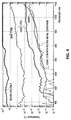
U.S. Patent Application Serial No. 11/461,457 , entitled IMAGE SENSOR AND METHOD FOR MANUFACTURING THE SAME, filed August 1,2006, the disclosure of which is herein incorporated by reference in its entirety. This application describes a method of forming the Optical Black layer by depositing a Ti/TiN layer over the top of the sensor passivation surface and immediately below the Color Filter Planarization layer (sees cross-sectional drawing inFig. 1 ). The thickness of the metal mask used for OB formation to render the OB pixel opaque can be adjusted to increase opacity and decrease light transmission into the OB pixel, but is typically on the order of 1000 Å when applied via standard sputtering means. By depositing the Ti/TiN layer over the sensor after the bulk of the critical steps are completed, basic pixel performance is separately optimized from OB performance with respect to opacity. In other words, pixel performance is optimized separately from the steps needed to optimize the properties of the optical black, color filters and microlenses. - Light transmission is rendered negligible by using the Ti/TiN overlayer as shown in the transmission plot of
Fig. 4 . While the overlayer blocks incident light from reaching the photodiode, it does not occlude the entire pixel area to enable annealing ions to diffuse through the sensor overlayers to the photodiode.Fig. 5A shows a top layer view of the pixel layout including the location of the Ti/TiN pad over the photodiode and under the microlens.Fig. 5B is a cross-section plan showing how the Ti/TiN metallization blocks light focused by the microlens, yet allows the photodiode diffusion to be accessible to annealing ions during the final processing steps. The optical black pixel structure ofFig. 5 is further described in related U.S. Patent Application No. TBD, entitled APPARATUS AND METHOD FOR FORMING OPTICAL BLACK PIXELS WITH UNIFORMLY LOW DARK CURRENT. - In addition to the separately formed Ti/TiN layer, the pixel array of
U.S. Serial No. 11/461,457 Fig. 2 . The primary blocks include: - 1. a physically isolated Clear Pixel array within the overall structure
- 2. clear dummy array regions that separate the Clear Pixel array from the supporting OB sub-array regions.
- 3. OB dummy array regions that may be optionally included in the dummy sub-arrays
- 4. optional guard band region comprising multiple N- diffusions that are heavily (3V) reverse biased to absorb excess minority carriers adjacent to areas of sensor self-emission during operation.
- The clear dummy sub-arrays of
Fig. 2 interconnect throughout the array and generally fill the physical space between the clear pixel array and the OB sub-arrays. Dummy arrays are also placed at the very edge of the array except when an optional n- guard band is used. The latter guard band is typically about 40 to 60 pixels wide, assuming pixel spacing of about 2µm, as a collecting guard band of at least 100µm width is needed to capture stray minority carriers that may be self-photogenerated or have been scattered or migrated from the clear pixel array or the peripheral circuits surrounding the entire pixel array.Fig. 2 shows an N- guard band located on the right side as it is assumed here that light-emitting digital circuits are present to the right of the pixel array. The N-guard band is composed of a series of diffusions formed with the same sensor implant and diffusion area as the clear pixels to also prevent creation of edge effects while forming an effective sink for stray minority carriers. - The schematic circuits of prior art clear pixels and dummy pixels are compared in
Fig. 3 . Previously, each dummy pixel photodiode was kept at 0V potential by physically connecting the Select signal (SLCT) to the photodiode diffusion and imposing the condition, for dummy pixels, that the SLCT signal be held at 0V. Such a bias condition corresponds to full well saturation and is therefore largely unfavorable for attracting large numbers of minority carriers in the typical p-type substrate (electron). Consequently, while this type guard band can capture a few stray photo-generated signals from the underlying bulk, it can not minimize dark current accumulation in the neighboring pixels. Most importantly, holding dummy pixels at 0V resulted in excess generation-recombination current compared to active pixels. - Pixels located at the periphery of the pixel array in imaging sensors, i.e., at the outside edges of the pixel structure, typically show an anomalous behavior that is often referred to as edge effect. For example, pixel dark current is often higher along the sensor perimeter. Hence, pixels belonging to, or in proximity of, the pixel array edges normally can not be used as imaging or OB pixels. To reduce the drawback of having imaging pixels too close to the pixel array edges, a certain number of clear pixels can be used as a buffering region. However, this approach results in a wasted silicon real estate and ultimately in higher product cost.
- Significant improvement in minimizing edge effects in the horizontal direction is achieved by using an improved type of dummy pixel. A key point is to devise the dummy pixel configuration so that it helps stabilize the local environment while deflecting minority carriers away from the edges of the pixel array and operating at a quiescent bias that best mimics clear pixels. Another key point is that the dummy pixel is not encumbered with optical black to further insure that its properties are virtually identical to those of clear pixels in the imaging array.
- The present invention includes a preferred embodiment of this isolation strategy. As shown in
Fig. 6 , the dummy pixel consists of a clear pixel that is configured with the reset transistor biased in soft reset mode. Those skilled in the art will appreciate that such a photodiode dynamically pulls minority carriers that are within one diffusion length toward this higher potential (Vaa-Vth; i.e., one threshold voltage below the analog supply voltage) rather than letting them drift in the substrate. By constantly keeping the dummy photodiodes biased in this very favorable electrical condition, the associated junctions collect the stray electrons (minority carriers) rather than letting them continue to drift and scatter through the substrate. The dummy photodiode of the preferred embodiment thus acts a sink for any stray electrons within a diffusion length of the junction. Consequently, this structure substantially reduces excess dark current generation along the edges of the pixel array and thereby eliminates the edge effect. -
Figure 6 further compares the configuration of a clear pixel to that of a dummy pixel. Aphotodiode 10 is connected to a source of a reset transistor M1. The gate and drain of the reset transistor M1 are connected to a reset line, which is set to the supply voltage of the circuit. Thephotodiode 10 diffusion of a dummy pixel is held in soft reset by biasing reset transistor M1 at just below its threshold voltage so that it is operating in the sub-threshold voltage region. In practical terms, since some amount of dark current will always be discharging thephotodiode 10, reset transistor M1 can be considered to be in subthreshold bias. In this regime, thephotodiode 10 is never directly connected to the RST node that is otherwise kept at a high potential such as the full analog supply voltage, e.g., 3V. Thephotodiode 10 is thus operated at a voltage that is one threshold voltage below 3V. This configuration intrinsically decouples the photodiode node from the drain of reset transistor M1 to advantageously decouple power supply noise from the OB photodiodes. This coupling noise would otherwise be injected from the power supply node into the pixel array substrate and result in loss of image quality. Hence the shielding mechanism provided by the reset transistor M1, by virtue of its being in the sub-threshold region rather than operating as a low impedance is provides a significant improvement. - The dummy pixel circuit further includes an amplifier transistor M2 having a gate connected to the
photodiode 10 and a source of the reset transistor M1. A drain of the amplifier transistor M2 is connected to the reset line. A readout transistor M3 has a drain connected to a source of the amplifier transistor M2, and a source connected to a read bus. A gate of the readout transistor M3 is preferably held at zero volts. - Compared to a clear pixel layout, this configuration of dummy pixels requires the removal of a "via" contact that would otherwise connect reset transistor M1 to the metal bus supporting reset across each row of pixels. This via contact is present in the clear pixels. It also requires connecting the gate of the reset transistor M1 to its drain terminal. This connection can be implemented by adding a
metal 1 bridge shape to the existing clear pixel layout. Since the OB modifications pose minimum intrusion to the clear pixel layout, they are perfectly suited in minimizing any impact to the symmetry of the pixel array to enable virtually identical behavior amongst the clear and OB pixels apart from response to light. - By setting operation in this thermal equilibrium condition, the RoA products of the dummy pixels are not degraded from the value set by the production process to match the intrinsic RoA products of the clear pixels. Similarly, the diode idealities of dummy and clear pixels also largely match such that the Shockley currents are effectively identical:


Claims (14)
- A dummy pixel comprising:a photodiode (10); anda reset transistor (M1) connected to the photodiode, wherein the reset transistor is configured to be biased in a soft reset mode by having a gate and drain connected to a reset line set to a first predetermined voltage and wherein the reset line is not connected to a reset bus.
- The dummy pixel of Claim 1 further comprising an amplifier transistor having a gate connected to the photodiode and a source of the reset transistor, and a drain connected to the reset line.
- The dummy pixel of Claim 2, , further comprising a readout transistor having a drain connected to a source of the amplifier transistor, and having a gate connected to a second predetermined voltage.
- The dummy pixel of Claim 3, wherein the first predetermined voltage is a circuit supply voltage.
- The dummy pixel of Claim 4, , wherein the second predetermined voltage is zero volts.
- The dummy pixel of Claim 1, wherein the photodiode forms a current sink for stray electrons.
- The dummy pixel of Claim 1 wherein the dummy pixel is formed as a clear pixel.
- The dummy pixel of claim 1, wherein the dummy pixel is formed as an optical black pixel.
- An image sensor comprising:an array of clear pixels;a plurality of sub-arrays of optical black pixels; anda plurality of sub-arrays of dummy pixels located between the array of clear pixels and the sub-arrays of optical black pixels, wherein each dummy pixel is a dummy pixel according to any preceding claim.
- The image sensor of claim 9 further comprising sub-arrays of dummy pixels located on a perimeter of the image sensor to reduce edge effects.
- A method for reducing dark current in an image sensor according to claim 9, the method comprising:forming at least one row or column of dummy pixels in an image sensor;wherein each dummy pixel comprises a pixel having a reset transistor permanently biased in a soft reset mode.
- The method of Claim 11, , wherein a photodiode in each dummy pixel acts a current sink for stray electrons.
- The method of Claim 11, , wherein the at least one row or column of dummy pixels is formed on a perimeter region of the image sensor to reduce edge effect.
- The method of Claim 11, , wherein the at least one row or column of dummy pixels is formed between sub-arrays of the image sensor to isolate the sub- arrays from each other.
Applications Claiming Priority (2)
| Application Number | Priority Date | Filing Date | Title |
|---|---|---|---|
| US11/715,736 US7755679B2 (en) | 2007-03-07 | 2007-03-07 | Apparatus and method for reducing edge effect in an image sensor |
| PCT/US2008/002242 WO2008108926A1 (en) | 2007-03-07 | 2008-02-20 | Apparatus and method for reducing edge effect in an image sensor |
Publications (3)
| Publication Number | Publication Date |
|---|---|
| EP2118919A1 EP2118919A1 (en) | 2009-11-18 |
| EP2118919A4 EP2118919A4 (en) | 2014-07-02 |
| EP2118919B1 true EP2118919B1 (en) | 2016-04-13 |
Family
ID=39738569
Family Applications (1)
| Application Number | Title | Priority Date | Filing Date |
|---|---|---|---|
| EP08725835.6A Active EP2118919B1 (en) | 2007-03-07 | 2008-02-20 | Apparatus and method for reducing edge effect in an image sensor |
Country Status (4)
| Country | Link |
|---|---|
| US (1) | US7755679B2 (en) |
| EP (1) | EP2118919B1 (en) |
| JP (1) | JP5260558B2 (en) |
| WO (1) | WO2008108926A1 (en) |
Families Citing this family (84)
| Publication number | Priority date | Publication date | Assignee | Title |
|---|---|---|---|---|
| GB2429864B (en) | 2005-09-01 | 2008-09-24 | Micron Technology Inc | Method and apparatus providing pixel array having automatic light control pixels and image capture pixels |
| WO2007052591A1 (en) * | 2005-11-02 | 2007-05-10 | Sharp Kabushiki Kaisha | Contents data output device, television having the device, and contents data output program |
| US7875840B2 (en) * | 2006-11-16 | 2011-01-25 | Aptina Imaging Corporation | Imager device with anti-fuse pixels and recessed color filter array |
| US8077236B2 (en) * | 2008-03-20 | 2011-12-13 | Aptina Imaging Corporation | Method and apparatus providing reduced metal routing in imagers |
| CN103501416B (en) | 2008-05-20 | 2017-04-12 | 派力肯成像公司 | Imaging system |
| US8866920B2 (en) | 2008-05-20 | 2014-10-21 | Pelican Imaging Corporation | Capturing and processing of images using monolithic camera array with heterogeneous imagers |
| US11792538B2 (en) | 2008-05-20 | 2023-10-17 | Adeia Imaging Llc | Capturing and processing of images including occlusions focused on an image sensor by a lens stack array |
| JP5335327B2 (en) | 2008-08-29 | 2013-11-06 | キヤノン株式会社 | Defect detection and correction apparatus and defect detection and correction method |
| US8872953B2 (en) * | 2009-10-30 | 2014-10-28 | Sony Corporation | Solid-state imaging device, manufacturing method thereof, camera, and electronic device |
| EP2502115A4 (en) | 2009-11-20 | 2013-11-06 | Pelican Imaging Corp | CAPTURE AND IMAGE PROCESSING USING A MONOLITHIC CAMERAS NETWORK EQUIPPED WITH HETEROGENEOUS IMAGERS |
| KR101824672B1 (en) * | 2010-05-12 | 2018-02-05 | 포토네이션 케이맨 리미티드 | Architectures for imager arrays and array cameras |
| US8878950B2 (en) | 2010-12-14 | 2014-11-04 | Pelican Imaging Corporation | Systems and methods for synthesizing high resolution images using super-resolution processes |
| JP5735318B2 (en) * | 2011-03-23 | 2015-06-17 | シャープ株式会社 | Solid-state imaging device and electronic information device |
| EP2708019B1 (en) | 2011-05-11 | 2019-10-16 | FotoNation Limited | Systems and methods for transmitting and receiving array camera image data |
| JP6115982B2 (en) * | 2011-07-04 | 2017-04-19 | ソニーセミコンダクタソリューションズ株式会社 | Imaging device and imaging apparatus |
| WO2013043751A1 (en) | 2011-09-19 | 2013-03-28 | Pelican Imaging Corporation | Systems and methods for controlling aliasing in images captured by an array camera for use in super resolution processing using pixel apertures |
| WO2013049699A1 (en) | 2011-09-28 | 2013-04-04 | Pelican Imaging Corporation | Systems and methods for encoding and decoding light field image files |
| EP2817955B1 (en) | 2012-02-21 | 2018-04-11 | FotoNation Cayman Limited | Systems and methods for the manipulation of captured light field image data |
| US9210392B2 (en) | 2012-05-01 | 2015-12-08 | Pelican Imaging Coporation | Camera modules patterned with pi filter groups |
| KR20150023907A (en) | 2012-06-28 | 2015-03-05 | 펠리칸 이매징 코포레이션 | Systems and methods for detecting defective camera arrays, optic arrays, and sensors |
| US20140002674A1 (en) | 2012-06-30 | 2014-01-02 | Pelican Imaging Corporation | Systems and Methods for Manufacturing Camera Modules Using Active Alignment of Lens Stack Arrays and Sensors |
| EP3869797B1 (en) | 2012-08-21 | 2023-07-19 | Adeia Imaging LLC | Method for depth detection in images captured using array cameras |
| EP2888698A4 (en) | 2012-08-23 | 2016-06-29 | Pelican Imaging Corp | HIGH RESOLUTION MOTION ESTIMATING BASED ON ELEMENTS FROM LOW RESOLUTION IMAGES CAPTURED WITH MATRIX SOURCE |
| US9214013B2 (en) | 2012-09-14 | 2015-12-15 | Pelican Imaging Corporation | Systems and methods for correcting user identified artifacts in light field images |
| EP4307659A1 (en) | 2012-09-28 | 2024-01-17 | Adeia Imaging LLC | Generating images from light fields utilizing virtual viewpoints |
| WO2014078443A1 (en) | 2012-11-13 | 2014-05-22 | Pelican Imaging Corporation | Systems and methods for array camera focal plane control |
| US9591242B2 (en) * | 2013-01-31 | 2017-03-07 | Taiwan Semiconductor Manufacturing Company, Ltd. | Black level control for image sensors |
| US9462164B2 (en) | 2013-02-21 | 2016-10-04 | Pelican Imaging Corporation | Systems and methods for generating compressed light field representation data using captured light fields, array geometry, and parallax information |
| WO2014133974A1 (en) | 2013-02-24 | 2014-09-04 | Pelican Imaging Corporation | Thin form computational and modular array cameras |
| WO2014138695A1 (en) | 2013-03-08 | 2014-09-12 | Pelican Imaging Corporation | Systems and methods for measuring scene information while capturing images using array cameras |
| US8866912B2 (en) | 2013-03-10 | 2014-10-21 | Pelican Imaging Corporation | System and methods for calibration of an array camera using a single captured image |
| US9521416B1 (en) | 2013-03-11 | 2016-12-13 | Kip Peli P1 Lp | Systems and methods for image data compression |
| WO2014164909A1 (en) | 2013-03-13 | 2014-10-09 | Pelican Imaging Corporation | Array camera architecture implementing quantum film sensors |
| US9124831B2 (en) | 2013-03-13 | 2015-09-01 | Pelican Imaging Corporation | System and methods for calibration of an array camera |
| US9519972B2 (en) | 2013-03-13 | 2016-12-13 | Kip Peli P1 Lp | Systems and methods for synthesizing images from image data captured by an array camera using restricted depth of field depth maps in which depth estimation precision varies |
| US9106784B2 (en) | 2013-03-13 | 2015-08-11 | Pelican Imaging Corporation | Systems and methods for controlling aliasing in images captured by an array camera for use in super-resolution processing |
| US9578259B2 (en) | 2013-03-14 | 2017-02-21 | Fotonation Cayman Limited | Systems and methods for reducing motion blur in images or video in ultra low light with array cameras |
| US9100586B2 (en) | 2013-03-14 | 2015-08-04 | Pelican Imaging Corporation | Systems and methods for photometric normalization in array cameras |
| WO2014150856A1 (en) | 2013-03-15 | 2014-09-25 | Pelican Imaging Corporation | Array camera implementing quantum dot color filters |
| US10122993B2 (en) | 2013-03-15 | 2018-11-06 | Fotonation Limited | Autofocus system for a conventional camera that uses depth information from an array camera |
| US9497429B2 (en) | 2013-03-15 | 2016-11-15 | Pelican Imaging Corporation | Extended color processing on pelican array cameras |
| US9445003B1 (en) | 2013-03-15 | 2016-09-13 | Pelican Imaging Corporation | Systems and methods for synthesizing high resolution images using image deconvolution based on motion and depth information |
| US9438888B2 (en) | 2013-03-15 | 2016-09-06 | Pelican Imaging Corporation | Systems and methods for stereo imaging with camera arrays |
| JP5886793B2 (en) | 2013-06-11 | 2016-03-16 | 浜松ホトニクス株式会社 | Solid-state imaging device |
| US9898856B2 (en) | 2013-09-27 | 2018-02-20 | Fotonation Cayman Limited | Systems and methods for depth-assisted perspective distortion correction |
| US9426343B2 (en) | 2013-11-07 | 2016-08-23 | Pelican Imaging Corporation | Array cameras incorporating independently aligned lens stacks |
| WO2015074078A1 (en) | 2013-11-18 | 2015-05-21 | Pelican Imaging Corporation | Estimating depth from projected texture using camera arrays |
| US9426361B2 (en) | 2013-11-26 | 2016-08-23 | Pelican Imaging Corporation | Array camera configurations incorporating multiple constituent array cameras |
| US10089740B2 (en) | 2014-03-07 | 2018-10-02 | Fotonation Limited | System and methods for depth regularization and semiautomatic interactive matting using RGB-D images |
| US9521319B2 (en) | 2014-06-18 | 2016-12-13 | Pelican Imaging Corporation | Array cameras and array camera modules including spectral filters disposed outside of a constituent image sensor |
| KR102155480B1 (en) | 2014-07-07 | 2020-09-14 | 삼성전자 주식회사 | Image sensor, image processing system including the same, and mobile electronic device including the same |
| CN113256730B (en) | 2014-09-29 | 2023-09-05 | 快图有限公司 | Systems and methods for dynamic calibration of array cameras |
| US12401911B2 (en) | 2014-11-07 | 2025-08-26 | Duelight Llc | Systems and methods for generating a high-dynamic range (HDR) pixel stream |
| US12401912B2 (en) | 2014-11-17 | 2025-08-26 | Duelight Llc | System and method for generating a digital image |
| CN114447010B (en) * | 2015-01-13 | 2025-03-21 | 索尼半导体解决方案公司 | Solid-state imaging device and electronic device |
| JP6515999B2 (en) * | 2015-03-30 | 2019-05-22 | 株式会社ニコン | Imaging device and imaging device |
| US9942474B2 (en) | 2015-04-17 | 2018-04-10 | Fotonation Cayman Limited | Systems and methods for performing high speed video capture and depth estimation using array cameras |
| US12445736B2 (en) | 2015-05-01 | 2025-10-14 | Duelight Llc | Systems and methods for generating a digital image |
| US11437418B2 (en) * | 2016-02-29 | 2022-09-06 | Sony Corporation | Solid-state image pickup device |
| US10685047B1 (en) | 2016-12-08 | 2020-06-16 | Townsend Street Labs, Inc. | Request processing system |
| JP6887856B2 (en) | 2017-04-11 | 2021-06-16 | ソニーセミコンダクタソリューションズ株式会社 | Solid-state image sensor |
| US10482618B2 (en) | 2017-08-21 | 2019-11-19 | Fotonation Limited | Systems and methods for hybrid depth regularization |
| EP3595291B1 (en) | 2018-07-11 | 2020-12-30 | IMEC vzw | An image sensor and a method for read-out of pixel signal |
| DE112020004391B4 (en) | 2019-09-17 | 2024-08-14 | Intrinsic Innovation Llc | Systems and methods for surface modeling using polarization features |
| CA3157194C (en) | 2019-10-07 | 2023-08-29 | Boston Polarimetrics, Inc. | Systems and methods for augmentation of sensor systems and imaging systems with polarization |
| CN114787648B (en) | 2019-11-30 | 2023-11-10 | 波士顿偏振测定公司 | Systems and methods for transparent object segmentation using polarization cues |
| FR3104814A1 (en) * | 2019-12-11 | 2021-06-18 | Isorg | Image sensor for electronic noise correction of a sensor |
| JP7462769B2 (en) | 2020-01-29 | 2024-04-05 | イントリンジック イノベーション エルエルシー | System and method for characterizing an object pose detection and measurement system - Patents.com |
| WO2021154459A1 (en) | 2020-01-30 | 2021-08-05 | Boston Polarimetrics, Inc. | Systems and methods for synthesizing data for training statistical models on different imaging modalities including polarized images |
| CN115004689B (en) | 2020-01-31 | 2025-12-16 | 索尼半导体解决方案公司 | Solid-state imaging element and imaging device |
| US11953700B2 (en) | 2020-05-27 | 2024-04-09 | Intrinsic Innovation Llc | Multi-aperture polarization optical systems using beam splitters |
| US12069227B2 (en) | 2021-03-10 | 2024-08-20 | Intrinsic Innovation Llc | Multi-modal and multi-spectral stereo camera arrays |
| US12020455B2 (en) | 2021-03-10 | 2024-06-25 | Intrinsic Innovation Llc | Systems and methods for high dynamic range image reconstruction |
| JP7279105B2 (en) | 2021-03-31 | 2023-05-22 | キヤノン株式会社 | Photoelectric conversion device |
| US11290658B1 (en) | 2021-04-15 | 2022-03-29 | Boston Polarimetrics, Inc. | Systems and methods for camera exposure control |
| US11954886B2 (en) | 2021-04-15 | 2024-04-09 | Intrinsic Innovation Llc | Systems and methods for six-degree of freedom pose estimation of deformable objects |
| CN120583841A (en) * | 2021-04-23 | 2025-09-02 | 武汉天马微电子有限公司 | Display panel and display device |
| US12067746B2 (en) | 2021-05-07 | 2024-08-20 | Intrinsic Innovation Llc | Systems and methods for using computer vision to pick up small objects |
| US12175741B2 (en) | 2021-06-22 | 2024-12-24 | Intrinsic Innovation Llc | Systems and methods for a vision guided end effector |
| US12340538B2 (en) | 2021-06-25 | 2025-06-24 | Intrinsic Innovation Llc | Systems and methods for generating and using visual datasets for training computer vision models |
| US12172310B2 (en) | 2021-06-29 | 2024-12-24 | Intrinsic Innovation Llc | Systems and methods for picking objects using 3-D geometry and segmentation |
| US11689813B2 (en) | 2021-07-01 | 2023-06-27 | Intrinsic Innovation Llc | Systems and methods for high dynamic range imaging using crossed polarizers |
| US12293535B2 (en) | 2021-08-03 | 2025-05-06 | Intrinsic Innovation Llc | Systems and methods for training pose estimators in computer vision |
| US12177582B2 (en) * | 2022-08-26 | 2024-12-24 | Canon Kabushiki Kaisha | Detector and detection system |
Family Cites Families (16)
| Publication number | Priority date | Publication date | Assignee | Title |
|---|---|---|---|---|
| US4387402A (en) | 1980-10-28 | 1983-06-07 | Texas Instruments Incorporated | Charge injection imaging device for faithful (dynamic) scene representation |
| JPS6181087A (en) | 1984-09-28 | 1986-04-24 | Olympus Optical Co Ltd | solid-state imaging device |
| JPH05244513A (en) * | 1992-02-26 | 1993-09-21 | Canon Inc | Photoelectric conversion device and driving method thereof |
| US6493030B1 (en) | 1998-04-08 | 2002-12-10 | Pictos Technologies, Inc. | Low-noise active pixel sensor for imaging arrays with global reset |
| US6697111B1 (en) | 1998-04-08 | 2004-02-24 | Ess Technology, Inc. | Compact low-noise active pixel sensor with progressive row reset |
| KR100284304B1 (en) * | 1998-12-22 | 2001-03-02 | 김영환 | CMOS image sensor and its driving method |
| JP2000196055A (en) * | 1998-12-24 | 2000-07-14 | Toshiba Corp | Solid-state imaging device |
| US6424375B1 (en) | 1999-09-21 | 2002-07-23 | Pixel Devices, International | Low noise active reset readout for image sensors |
| JP2001339643A (en) * | 2000-05-30 | 2001-12-07 | Nec Corp | Black level generation circuit for solid-state imaging device and solid-state imaging device |
| WO2003024091A1 (en) * | 2000-11-16 | 2003-03-20 | California Institute Of Technology | Photodiode cmos imager with column-feedback soft-reset |
| US6777660B1 (en) * | 2002-02-04 | 2004-08-17 | Smal Technologies | CMOS active pixel with reset noise reduction |
| US6911640B1 (en) * | 2002-04-30 | 2005-06-28 | Ess Technology, Inc. | Reducing reset noise in CMOS image sensors |
| US7172922B2 (en) * | 2002-08-19 | 2007-02-06 | Tower Semiconductor Ltd. | CMOS image sensor array with black pixel using negative-tone resist support layer |
| JP4242258B2 (en) * | 2003-11-21 | 2009-03-25 | シャープ株式会社 | Solid-state image sensor |
| US7760258B2 (en) * | 2007-03-07 | 2010-07-20 | Altasens, Inc. | Apparatus and method for stabilizing image sensor black level |
| US7999340B2 (en) * | 2007-03-07 | 2011-08-16 | Altasens, Inc. | Apparatus and method for forming optical black pixels with uniformly low dark current |
-
2007
- 2007-03-07 US US11/715,736 patent/US7755679B2/en active Active
-
2008
- 2008-02-20 JP JP2009552685A patent/JP5260558B2/en active Active
- 2008-02-20 WO PCT/US2008/002242 patent/WO2008108926A1/en not_active Ceased
- 2008-02-20 EP EP08725835.6A patent/EP2118919B1/en active Active
Also Published As
| Publication number | Publication date |
|---|---|
| US7755679B2 (en) | 2010-07-13 |
| EP2118919A4 (en) | 2014-07-02 |
| WO2008108926A1 (en) | 2008-09-12 |
| JP5260558B2 (en) | 2013-08-14 |
| US20080218608A1 (en) | 2008-09-11 |
| JP2010520708A (en) | 2010-06-10 |
| EP2118919A1 (en) | 2009-11-18 |
Similar Documents
| Publication | Publication Date | Title |
|---|---|---|
| EP2118919B1 (en) | Apparatus and method for reducing edge effect in an image sensor | |
| EP2980852B1 (en) | Solid-state image sensing element and imaging system | |
| US8411174B2 (en) | Shielding black reference pixels in image sensors | |
| US7429764B2 (en) | Signal processing device and image pickup apparatus using the same | |
| US7456880B2 (en) | Photoelectric conversion element having a plurality of semiconductor regions and including conductive layers provided on each isolation element region | |
| US7804116B2 (en) | Solid-state imaging device | |
| US7616355B2 (en) | Solid-state imaging device | |
| US9026972B2 (en) | Solid-state imaging device, camera, and design method for solid-state imaging device | |
| TWI478331B (en) | Back side illumination image sensor with reduced halo and electric shutter | |
| US6169318B1 (en) | CMOS imager with improved sensitivity | |
| US20070090274A1 (en) | Image sensors including active pixel sensor arrays | |
| US20090219422A1 (en) | Image capturing apparatus and electronic information device | |
| KR19980071795A (en) | Active pixel image sensor and active pixel sensor | |
| CN102208420A (en) | Solid-state image pickup element and image pickup apparatus | |
| TWI629771B (en) | Solid-state imaging element and manufacturing method thereof, and imaging device | |
| US7999340B2 (en) | Apparatus and method for forming optical black pixels with uniformly low dark current | |
| US20180166482A1 (en) | Unit pixel for image sensor comprising contact pad connected to light receiving portion | |
| EP1505655B1 (en) | Solid state image pickup device and camera using the solid state image pickup device | |
| US20090008686A1 (en) | Solid-state imaging device with improved charge transfer efficiency | |
| JP2009505437A (en) | Method and apparatus for protecting correction pixels from false charges in an imager | |
| US11545525B2 (en) | Imaging device | |
| EP2249386B1 (en) | Imaging device | |
| US20080211050A1 (en) | Image sensor with inter-pixel isolation | |
| US7442974B2 (en) | Image sensor with inter-pixel isolation | |
| US20050184321A1 (en) | Low dark current CMOS image sensor pixel having a photodiode isolated from field oxide |
Legal Events
| Date | Code | Title | Description |
|---|---|---|---|
| PUAI | Public reference made under article 153(3) epc to a published international application that has entered the european phase |
Free format text: ORIGINAL CODE: 0009012 |
|
| 17P | Request for examination filed |
Effective date: 20090910 |
|
| AK | Designated contracting states |
Kind code of ref document: A1 Designated state(s): AT BE BG CH CY CZ DE DK EE ES FI FR GB GR HR HU IE IS IT LI LT LU LV MC MT NL NO PL PT RO SE SI SK TR |
|
| DAX | Request for extension of the european patent (deleted) | ||
| A4 | Supplementary search report drawn up and despatched |
Effective date: 20140604 |
|
| RIC1 | Information provided on ipc code assigned before grant |
Ipc: H04N 5/369 20110101AFI20140528BHEP Ipc: H01L 27/146 20060101ALI20140528BHEP |
|
| REG | Reference to a national code |
Ref country code: DE Ref legal event code: R079 Ref document number: 602008043496 Country of ref document: DE Free format text: PREVIOUS MAIN CLASS: H01L0021000000 Ipc: H04N0005361000 |
|
| GRAP | Despatch of communication of intention to grant a patent |
Free format text: ORIGINAL CODE: EPIDOSNIGR1 |
|
| INTG | Intention to grant announced |
Effective date: 20151211 |
|
| RIC1 | Information provided on ipc code assigned before grant |
Ipc: H04N 5/361 20110101AFI20151201BHEP Ipc: H01L 27/146 20060101ALI20151201BHEP Ipc: H04N 5/369 20110101ALI20151201BHEP |
|
| GRAS | Grant fee paid |
Free format text: ORIGINAL CODE: EPIDOSNIGR3 |
|
| GRAA | (expected) grant |
Free format text: ORIGINAL CODE: 0009210 |
|
| RAP1 | Party data changed (applicant data changed or rights of an application transferred) |
Owner name: ALTASENS, INC. |
|
| AK | Designated contracting states |
Kind code of ref document: B1 Designated state(s): AT BE BG CH CY CZ DE DK EE ES FI FR GB GR HR HU IE IS IT LI LT LU LV MC MT NL NO PL PT RO SE SI SK TR |
|
| REG | Reference to a national code |
Ref country code: GB Ref legal event code: FG4D |
|
| REG | Reference to a national code |
Ref country code: AT Ref legal event code: REF Ref document number: 791188 Country of ref document: AT Kind code of ref document: T Effective date: 20160415 Ref country code: CH Ref legal event code: EP |
|
| REG | Reference to a national code |
Ref country code: IE Ref legal event code: FG4D |
|
| REG | Reference to a national code |
Ref country code: DE Ref legal event code: R096 Ref document number: 602008043496 Country of ref document: DE |
|
| REG | Reference to a national code |
Ref country code: NL Ref legal event code: FP |
|
| REG | Reference to a national code |
Ref country code: LT Ref legal event code: MG4D |
|
| REG | Reference to a national code |
Ref country code: AT Ref legal event code: MK05 Ref document number: 791188 Country of ref document: AT Kind code of ref document: T Effective date: 20160413 |
|
| PG25 | Lapsed in a contracting state [announced via postgrant information from national office to epo] |
Ref country code: LT Free format text: LAPSE BECAUSE OF FAILURE TO SUBMIT A TRANSLATION OF THE DESCRIPTION OR TO PAY THE FEE WITHIN THE PRESCRIBED TIME-LIMIT Effective date: 20160413 Ref country code: NO Free format text: LAPSE BECAUSE OF FAILURE TO SUBMIT A TRANSLATION OF THE DESCRIPTION OR TO PAY THE FEE WITHIN THE PRESCRIBED TIME-LIMIT Effective date: 20160713 Ref country code: PL Free format text: LAPSE BECAUSE OF FAILURE TO SUBMIT A TRANSLATION OF THE DESCRIPTION OR TO PAY THE FEE WITHIN THE PRESCRIBED TIME-LIMIT Effective date: 20160413 Ref country code: FI Free format text: LAPSE BECAUSE OF FAILURE TO SUBMIT A TRANSLATION OF THE DESCRIPTION OR TO PAY THE FEE WITHIN THE PRESCRIBED TIME-LIMIT Effective date: 20160413 |
|
| PG25 | Lapsed in a contracting state [announced via postgrant information from national office to epo] |
Ref country code: GR Free format text: LAPSE BECAUSE OF FAILURE TO SUBMIT A TRANSLATION OF THE DESCRIPTION OR TO PAY THE FEE WITHIN THE PRESCRIBED TIME-LIMIT Effective date: 20160714 Ref country code: ES Free format text: LAPSE BECAUSE OF FAILURE TO SUBMIT A TRANSLATION OF THE DESCRIPTION OR TO PAY THE FEE WITHIN THE PRESCRIBED TIME-LIMIT Effective date: 20160413 Ref country code: AT Free format text: LAPSE BECAUSE OF FAILURE TO SUBMIT A TRANSLATION OF THE DESCRIPTION OR TO PAY THE FEE WITHIN THE PRESCRIBED TIME-LIMIT Effective date: 20160413 Ref country code: PT Free format text: LAPSE BECAUSE OF FAILURE TO SUBMIT A TRANSLATION OF THE DESCRIPTION OR TO PAY THE FEE WITHIN THE PRESCRIBED TIME-LIMIT Effective date: 20160816 Ref country code: SE Free format text: LAPSE BECAUSE OF FAILURE TO SUBMIT A TRANSLATION OF THE DESCRIPTION OR TO PAY THE FEE WITHIN THE PRESCRIBED TIME-LIMIT Effective date: 20160413 Ref country code: HR Free format text: LAPSE BECAUSE OF FAILURE TO SUBMIT A TRANSLATION OF THE DESCRIPTION OR TO PAY THE FEE WITHIN THE PRESCRIBED TIME-LIMIT Effective date: 20160413 Ref country code: LV Free format text: LAPSE BECAUSE OF FAILURE TO SUBMIT A TRANSLATION OF THE DESCRIPTION OR TO PAY THE FEE WITHIN THE PRESCRIBED TIME-LIMIT Effective date: 20160413 |
|
| PG25 | Lapsed in a contracting state [announced via postgrant information from national office to epo] |
Ref country code: BE Free format text: LAPSE BECAUSE OF FAILURE TO SUBMIT A TRANSLATION OF THE DESCRIPTION OR TO PAY THE FEE WITHIN THE PRESCRIBED TIME-LIMIT Effective date: 20160413 Ref country code: IT Free format text: LAPSE BECAUSE OF FAILURE TO SUBMIT A TRANSLATION OF THE DESCRIPTION OR TO PAY THE FEE WITHIN THE PRESCRIBED TIME-LIMIT Effective date: 20160413 |
|
| REG | Reference to a national code |
Ref country code: FR Ref legal event code: PLFP Year of fee payment: 10 |
|
| REG | Reference to a national code |
Ref country code: DE Ref legal event code: R097 Ref document number: 602008043496 Country of ref document: DE |
|
| PG25 | Lapsed in a contracting state [announced via postgrant information from national office to epo] |
Ref country code: SK Free format text: LAPSE BECAUSE OF FAILURE TO SUBMIT A TRANSLATION OF THE DESCRIPTION OR TO PAY THE FEE WITHIN THE PRESCRIBED TIME-LIMIT Effective date: 20160413 Ref country code: DK Free format text: LAPSE BECAUSE OF FAILURE TO SUBMIT A TRANSLATION OF THE DESCRIPTION OR TO PAY THE FEE WITHIN THE PRESCRIBED TIME-LIMIT Effective date: 20160413 Ref country code: EE Free format text: LAPSE BECAUSE OF FAILURE TO SUBMIT A TRANSLATION OF THE DESCRIPTION OR TO PAY THE FEE WITHIN THE PRESCRIBED TIME-LIMIT Effective date: 20160413 Ref country code: RO Free format text: LAPSE BECAUSE OF FAILURE TO SUBMIT A TRANSLATION OF THE DESCRIPTION OR TO PAY THE FEE WITHIN THE PRESCRIBED TIME-LIMIT Effective date: 20160413 Ref country code: CZ Free format text: LAPSE BECAUSE OF FAILURE TO SUBMIT A TRANSLATION OF THE DESCRIPTION OR TO PAY THE FEE WITHIN THE PRESCRIBED TIME-LIMIT Effective date: 20160413 |
|
| PLBE | No opposition filed within time limit |
Free format text: ORIGINAL CODE: 0009261 |
|
| STAA | Information on the status of an ep patent application or granted ep patent |
Free format text: STATUS: NO OPPOSITION FILED WITHIN TIME LIMIT |
|
| 26N | No opposition filed |
Effective date: 20170116 |
|
| PG25 | Lapsed in a contracting state [announced via postgrant information from national office to epo] |
Ref country code: SI Free format text: LAPSE BECAUSE OF FAILURE TO SUBMIT A TRANSLATION OF THE DESCRIPTION OR TO PAY THE FEE WITHIN THE PRESCRIBED TIME-LIMIT Effective date: 20160413 |
|
| PG25 | Lapsed in a contracting state [announced via postgrant information from national office to epo] |
Ref country code: MC Free format text: LAPSE BECAUSE OF FAILURE TO SUBMIT A TRANSLATION OF THE DESCRIPTION OR TO PAY THE FEE WITHIN THE PRESCRIBED TIME-LIMIT Effective date: 20160413 |
|
| REG | Reference to a national code |
Ref country code: CH Ref legal event code: PL |
|
| REG | Reference to a national code |
Ref country code: NL Ref legal event code: MM Effective date: 20170301 |
|
| PG25 | Lapsed in a contracting state [announced via postgrant information from national office to epo] |
Ref country code: LI Free format text: LAPSE BECAUSE OF NON-PAYMENT OF DUE FEES Effective date: 20170228 Ref country code: CH Free format text: LAPSE BECAUSE OF NON-PAYMENT OF DUE FEES Effective date: 20170228 |
|
| REG | Reference to a national code |
Ref country code: IE Ref legal event code: MM4A |
|
| PG25 | Lapsed in a contracting state [announced via postgrant information from national office to epo] |
Ref country code: NL Free format text: LAPSE BECAUSE OF NON-PAYMENT OF DUE FEES Effective date: 20170301 |
|
| PG25 | Lapsed in a contracting state [announced via postgrant information from national office to epo] |
Ref country code: LU Free format text: LAPSE BECAUSE OF NON-PAYMENT OF DUE FEES Effective date: 20170220 |
|
| REG | Reference to a national code |
Ref country code: FR Ref legal event code: PLFP Year of fee payment: 11 |
|
| PG25 | Lapsed in a contracting state [announced via postgrant information from national office to epo] |
Ref country code: IE Free format text: LAPSE BECAUSE OF NON-PAYMENT OF DUE FEES Effective date: 20170220 |
|
| REG | Reference to a national code |
Ref country code: DE Ref legal event code: R081 Ref document number: 602008043496 Country of ref document: DE Owner name: SAMSUNG ELECTRONICS CO., LTD., SUWON CITY, KR Free format text: FORMER OWNER: ALTASENS, INC., WESTLAKE VILLAGE, CALIF., US Ref country code: DE Ref legal event code: R082 Ref document number: 602008043496 Country of ref document: DE Representative=s name: LORENZ & KOLLEGEN PATENTANWAELTE PARTNERSCHAFT, DE Ref country code: DE Ref legal event code: R081 Ref document number: 602008043496 Country of ref document: DE Owner name: JVC KENWOOD CORP., YOKOHAMA-SHI, JP Free format text: FORMER OWNER: ALTASENS, INC., WESTLAKE VILLAGE, CALIF., US |
|
| REG | Reference to a national code |
Ref country code: GB Ref legal event code: 732E Free format text: REGISTERED BETWEEN 20180524 AND 20180530 |
|
| REG | Reference to a national code |
Ref country code: FR Ref legal event code: TP Owner name: JVC KENWOOD CORPORATION, JP Effective date: 20180725 |
|
| PG25 | Lapsed in a contracting state [announced via postgrant information from national office to epo] |
Ref country code: MT Free format text: LAPSE BECAUSE OF NON-PAYMENT OF DUE FEES Effective date: 20170220 |
|
| PG25 | Lapsed in a contracting state [announced via postgrant information from national office to epo] |
Ref country code: HU Free format text: LAPSE BECAUSE OF FAILURE TO SUBMIT A TRANSLATION OF THE DESCRIPTION OR TO PAY THE FEE WITHIN THE PRESCRIBED TIME-LIMIT; INVALID AB INITIO Effective date: 20080220 |
|
| REG | Reference to a national code |
Ref country code: GB Ref legal event code: 732E Free format text: REGISTERED BETWEEN 20190725 AND 20190731 |
|
| REG | Reference to a national code |
Ref country code: DE Ref legal event code: R082 Ref document number: 602008043496 Country of ref document: DE Representative=s name: LORENZ & KOLLEGEN PATENTANWAELTE PARTNERSCHAFT, DE Ref country code: DE Ref legal event code: R081 Ref document number: 602008043496 Country of ref document: DE Owner name: SAMSUNG ELECTRONICS CO., LTD., SUWON CITY, KR Free format text: FORMER OWNER: JVC KENWOOD CORP., YOKOHAMA-SHI, KANAGAWA, JP |
|
| PG25 | Lapsed in a contracting state [announced via postgrant information from national office to epo] |
Ref country code: BG Free format text: LAPSE BECAUSE OF FAILURE TO SUBMIT A TRANSLATION OF THE DESCRIPTION OR TO PAY THE FEE WITHIN THE PRESCRIBED TIME-LIMIT Effective date: 20160413 |
|
| PG25 | Lapsed in a contracting state [announced via postgrant information from national office to epo] |
Ref country code: CY Free format text: LAPSE BECAUSE OF NON-PAYMENT OF DUE FEES Effective date: 20160413 |
|
| PG25 | Lapsed in a contracting state [announced via postgrant information from national office to epo] |
Ref country code: TR Free format text: LAPSE BECAUSE OF FAILURE TO SUBMIT A TRANSLATION OF THE DESCRIPTION OR TO PAY THE FEE WITHIN THE PRESCRIBED TIME-LIMIT Effective date: 20160413 |
|
| PG25 | Lapsed in a contracting state [announced via postgrant information from national office to epo] |
Ref country code: IS Free format text: LAPSE BECAUSE OF FAILURE TO SUBMIT A TRANSLATION OF THE DESCRIPTION OR TO PAY THE FEE WITHIN THE PRESCRIBED TIME-LIMIT Effective date: 20160813 |
|
| REG | Reference to a national code |
Ref country code: DE Ref legal event code: R079 Ref document number: 602008043496 Country of ref document: DE Free format text: PREVIOUS MAIN CLASS: H04N0005361000 Ipc: H04N0025630000 |
|
| P01 | Opt-out of the competence of the unified patent court (upc) registered |
Effective date: 20230524 |
|
| PGFP | Annual fee paid to national office [announced via postgrant information from national office to epo] |
Ref country code: DE Payment date: 20241224 Year of fee payment: 18 |
|
| PGFP | Annual fee paid to national office [announced via postgrant information from national office to epo] |
Ref country code: GB Payment date: 20250102 Year of fee payment: 18 |
|
| PGFP | Annual fee paid to national office [announced via postgrant information from national office to epo] |
Ref country code: FR Payment date: 20251222 Year of fee payment: 19 |