EP2115845B1 - Vorrichtung zum überwachen von ableitvorgängen in einem leiter eines mittel- oder hochspannungssystems - Google Patents
Vorrichtung zum überwachen von ableitvorgängen in einem leiter eines mittel- oder hochspannungssystems Download PDFInfo
- Publication number
- EP2115845B1 EP2115845B1 EP08708298.8A EP08708298A EP2115845B1 EP 2115845 B1 EP2115845 B1 EP 2115845B1 EP 08708298 A EP08708298 A EP 08708298A EP 2115845 B1 EP2115845 B1 EP 2115845B1
- Authority
- EP
- European Patent Office
- Prior art keywords
- monitoring device
- transformer
- memory circuit
- monitoring
- conductor
- Prior art date
- Legal status (The legal status is an assumption and is not a legal conclusion. Google has not performed a legal analysis and makes no representation as to the accuracy of the status listed.)
- Not-in-force
Links
Images
Classifications
-
- H—ELECTRICITY
- H02—GENERATION; CONVERSION OR DISTRIBUTION OF ELECTRIC POWER
- H02H—EMERGENCY PROTECTIVE CIRCUIT ARRANGEMENTS
- H02H3/00—Emergency protective circuit arrangements for automatic disconnection directly responsive to an undesired change from normal electric working condition with or without subsequent reconnection ; integrated protection
- H02H3/02—Details
- H02H3/04—Details with warning or supervision in addition to disconnection, e.g. for indicating that protective apparatus has functioned
- H02H3/048—Checking overvoltage diverters
-
- H—ELECTRICITY
- H02—GENERATION; CONVERSION OR DISTRIBUTION OF ELECTRIC POWER
- H02H—EMERGENCY PROTECTIVE CIRCUIT ARRANGEMENTS
- H02H1/00—Details of emergency protective circuit arrangements
- H02H1/0007—Details of emergency protective circuit arrangements concerning the detecting means
Definitions
- the invention relates to a device for monitoring discharge processes in a conductor of a medium or high voltage system, which has at least one transducer which is suitable for detecting a current flowing in the conductor, wherein the at least one transducer is in communication with a monitoring device for monitoring the discharge process ,
- a device of this kind is for example from the WO 02/061904 A1 known. It is used for so-called arrester monitoring, in which a current flowing in the conductor of a medium or high-voltage system is monitored.
- the invention has the object of developing a device of the type mentioned. It is intended to provide a monitoring device for discharge processes, which can remain in a power-saving passive mode until a discharge process is to be logged. In this case, the device should be able to boot into the active mode in order to record a discharge process, even if this only one takes a very short time. Nevertheless, the complete discharge process should be able to be logged, even if it already takes place during a "wake-up phase" of the monitoring device and possibly has already been completed at the end of it.
- the solution of this problem by the invention is in a device of the type mentioned in that between the transducer and the monitoring device of the device, a trigger is arranged, which exceeds the monitoring device of a not suitable for monitoring passive above a threshold current flowing in the conductor. Mode is set in an active mode suitable for monitoring, and that between the converter and the monitoring device, a memory circuit is arranged, which stores the to be monitored by the monitoring device and / or to be logged leakage current.
- An essential feature of the invention is therefore a memory circuit for the current to be logged, in which a signal corresponding to the current flowing through the conductor is stored until the monitoring device has been brought up from a stand-by mode to an active state. Then, the signal stored in the memory circuit is recorded.
- a first development of the invention provides that the trigger is connected to a first converter and that the memory circuit is connected to a second converter. After that, therefore, two separate transducers are provided, which are coupled to the conductor and independently supply the trigger or the memory circuit with the current signal.
- At least one converter can be designed as a current transformer.
- the current transformer may have an iron core.
- At least one transducer can also be designed as an ironless magnetic field probe.
- the memory circuit may include at least one resistor and at least one capacitor.
- a rectifier is arranged between the converter and the memory circuit.
- the rectifier can be a bridge rectifier, in particular a two-way rectifier. It can also be a one-way rectifier.
- a protective circuit is arranged between the converter and the memory circuit.
- a protective circuit can also be arranged between the memory circuit and the monitoring device.
- the monitoring device may also be associated with a discharge circuit with which the storage circuit can be discharged after recording the leakage current.
- the monitoring device has an analog-to-digital converter and a reference associated therewith in order to be able to record the leakage current to be logged in a simple and known manner.
- the device for monitoring the discharge process and in particular the memory circuit are constructed so that they do not require any supply voltage and thus has no power consumption. This supports the goal of a power-saving option for arrester monitoring.
- the device is constantly ready for use without delay. Leakage currents can be detected reliably, even if they take only extremely short time. This is the prerequisite for a reliable monitoring and recording of only sporadically occurring and unpredictable discharge processes.
- the memory circuit is constructed so that it is independent of the monitoring device. This creates the prerequisite for putting the monitoring device in a desired "power-save” mode.
- the memory circuit may take over the storage of the surge impulse until the monitoring device has completed its run-up from the "power-save” mode to the normal operating state and can perform the further processing. This is an essential prerequisite for being able to put the monitoring device in a desired energy-saving "power-save” mode, without running the risk of being unable to detect parts of the discharge process.
- the memory circuit which is preferably designed as a resistor-capacitor network, is constructed such that it can already carry out a preprocessing of the signal to be detected.
- the preprocessing may be designed to form the peak or average of the signal to be detected, depending on the ratio of the resistors to the capacitor.
- two separate memory circuits for the peak or the mean are also two separate memory circuits for the peak or the mean. This "analog-computational" preprocessing reduces the computational further processing by the monitoring device. This contributes to the further optimization of the power consumption of the device.
- Discharge processes are very rare and have only a short duration. For this reason, the monitoring device is required only a tiny fraction of the total time. This idle time is almost 100% with regard to the detection of the discharge processes.
- the monitoring device with the analog-to-digital converter and the reference is designed so that it can be put in the "power-save" mode during the time it is not needed. This means an optimization of the power requirement.
- the prerequisite is created to realize a self-powered and economical device for the monitoring of leakage processes.
- the invention provides for the monitoring of the current, a stationary and compact device available, which is arranged on the arrester.
- the device has its own independent power supply. This can be a battery or a solar cell; It is also a power supply from Ableiterleckströmen conceivable. Therefore, it is advantageous that the monitoring device can be operated in a power-saving manner (so-called "intelligent and energy-self-sufficient sensor system").
- a permanent active state of the device which consumes a lot of power even when using the most power-saving circuits (microcontroller, analog-to-digital converter, etc.), is not required. Therefore, the proposed device is placed in a low-power passive mode, ie in a "power-save mode" similar to a "stand-by" operation in which the device has only a minimal power consumption (current flows of a few ⁇ A).
- the wake-up time to move the monitor from its passive to active state is in the range of 50 microseconds to the millisecond range, depending on the type of circuit. In most cases, the necessary analog circuit parts, such as. As the reference of an analog-to-digital converter of the monitor, a lot of time for startup and settling in the stable state.
- a device of the generic type which, as explained, is in a power-save mode and must first be "woken up” when a discharge process occurs and then requires a certain time to reach full operational readiness, but according to the invention is not problematical, but rather the typically only short-lasting discharges can still be detected completely.
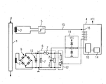
- FIG. 1 An embodiment of the invention is shown.
- the single figure shows schematically a device for monitoring discharge processes in a conductor of a medium or high voltage system with their components.
- a conductor 1 of a medium or high voltage system can be seen. If there is a discharge process, a surge I flows through the conductor 1. A to the conductor 1 inductively coupled current transformer 1 detects this surge I and converts it into an analog voltage signal. With this voltage signal a trigger 5 (trigger circuit) is fed. If the surge I exceeds a predetermined Threshold, ie a threshold current I s , the trigger 5 generates an active trigger signal 15. This trigger signal 15 wakes a monitoring device 4 from a "standby" or. "Power Save” mode and puts them in an active, fully operational state in which they can log the leakage current; So it takes place in the monitoring device 4, a startup and an initialization.
- Threshold ie a threshold current I s
- the trigger signal 15 is fed to the monitoring device 4 at an interrupt-capable input 16.
- the monitoring device 4 itself has a powerful microcontroller. Shown are an integrated analog-to-digital converter 13 and a required analog reference 14 (reference voltage).
- the surge I acts not only on the current transformer 2 but at the same time on a second converter 3, which is executed in the embodiment as an ironless magnetic field probe.
- the converter 3 is designed as a current transformer with iron core.
- the current I flowing in the conductor 1 generates a proportional magnetic field around the conductor 1, which is detected by the transducer 3 and converted into a proportional current Ip.
- This current I P is rectified by a rectifier 9 and supplied to a memory circuit 6, which is designed as a resistor-capacitor network.
- the rectifier 9 formed in the embodiment as a bridge rectifier (two-way rectifier) can also be designed as a one-way rectifier. Using two separate detection circuits with opposite rectification, one can distinguish between positive and negative surges.
- the resistors 7 and the capacitor 8 contained in the memory circuit 6 determine the charging or the discharge time constant of the memory circuit and thus the magnitude of the voltage across the capacitor 8, which is caused by the current I P.
- the existing in the memory circuit 6 capacitor 8 thus serves as a memory element.
- the voltage across the capacitor 8 is supplied to the analog-to-digital converter 13.
- the monitoring device 4 After the monitoring device 4 has performed its run-up and the initialization and completed, it immediately begins with the digitization of the analog voltage at the capacitor 8 by means of the analog-to-digital converter 13.
- the obtained digitized voltage value can be used for further processing in the sense of the known arrester monitoring become.
- the capacitor 8 can be discharged quickly with a discharge circuit 12, wherein the activation of the discharge circuit 12 is carried out by the monitoring device 4 as shown.
- the memory circuit 6 is ready for a new storage of a discharge process (readiness of detection).
- the illustrated monitoring device 4 may also be constructed discretely, consisting of a controller and an external analog-to-digital converter 13 and associated reference 14th
- protective circuits 10 and 11 are provided, which are arranged between the rectifier 9 and the memory circuit 6 or between the memory circuit 6 and the monitoring unit 4.
- the protective circuits 10 and 11 are intended to protect the respective subsequent circuit parts from overvoltage.
- the protective circuits are 10, 11 not required for the detection of the Ableitvor Vietnamese, they merely produce an increase in the robustness of the device.
- transducers 2 and 3 are combined to form a single transducer.
- resistors 7 and the capacitor 8 determine, as explained, the charging or the discharge time constant of the memory circuit 6, so the network, and thus the amount of voltage across the capacitor 8.
- the detection of the Ableitvor Vietnamese can be changed so that it detects the peak value ("peak hold") or the average value ("Average") of the surge I.
- Two acquisitions can also be set up in parallel to determine both values. In this case, so z. B. two parallel memory circuits 4 are provided.
- this voltage can also be digitized cyclically in the sense of a temporal sampling. With a constant and known sampling interval, this gives rise to further possibilities for evaluating the voltage values in the sense of arrester monitoring.
- the time duration of the discharge process can be determined as follows: The time from the active trigger signal 15 to the first digitization of the voltage across the capacitor 8 can be assumed to be known and constant (system-immanent). The number of samples until a decay of the Voltage at the capacitor 8 and thus the surge I is detected can be determined.
- the energy equivalent that is of interest for the arrester monitoring can be calculated with the determined average value and the determined duration of the discharge process. H. How much energy did the arrester have to absorb during the discharge process (this contributes significantly to its aging).
- a memory element in the form of the capacitor 8 with integrating property is advantageously supplemented with the differentiating property of the converter 3, which in the exemplary embodiment is implemented as an inductively operating magnetic field probe in order to form an analogue image of the current surge I flowing in the arrester.
- This advantageously supports the concept of performing a preprocessing of the signal to be detected outside the monitoring device 4.
- the monitoring device 4 only after its startup with the digitization of the voltage across the capacitor 8 begins, has the further advantage that the high-energy impulse I has already decayed in the arrester 1, when the digitization is started.
- the surges possible during discharge processes can go as far as 100 kA. This is associated with high electrical spring, the electronics, z. As the sensitive analog-to-digital conversion, can interfere.
- the temporal staggering of the processing cleverly avoids the otherwise unavoidable influence of high-energy surges through the coupling (EMC) of disturbances.
- EMC coupling
- a spatial separation of the transducer 3 and the monitoring device 4 (including the parts 13 and 14) prohibits the desired efficiency of the device, because in this case no more advantageous compact design would be possible. Due to the method of operation described, however, this does not cause a problem in the proposed solution.
Landscapes
- Measurement Of Current Or Voltage (AREA)
- Testing Relating To Insulation (AREA)
- Testing Of Short-Circuits, Discontinuities, Leakage, Or Incorrect Line Connections (AREA)
- Gas-Insulated Switchgears (AREA)
Description
- Die Erfindung betrifft eine Vorrichtung zum Überwachen von Ableitvorgängen in einem Leiter eines Mittel- oder Hochspannungssystems, die mindestens einen Wandler aufweist, der zur Erfassung eines im Leiter fließenden Stroms geeignet ist, wobei der mindestens eine Wandler mit einer Überwachungseinrichtung zur Überwachung des Ableitvorgangs in Verbindung steht.
- Eine Vorrichtung dieser Art ist beispielsweise aus der
WO 02/061904 A1 - Die Aufzeichnung bzw. Bewertung derartiger Stromstöße ist aus Sicht des Ableitermonitoring sehr wichtig. Die zu überwachenden Ableitvorgänge treten allerdings sehr selten auf und haben nur eine sehr kurze Dauer. Die typische Rückenhalbwertzeit der Stromstöße ist kleiner als 100 µs. Ihr Eintreten ist nicht vorhersehbar. Die Erfassung dieser Vorgänge erfordert leistungsfähige Rechnersysteme, insbesondere was die Digitalisierung, die Quantifizierung und die Bewertung anbelangt.
- Der Erfindung liegt die Aufgabe zugrunde, eine Vorrichtung der eingangs genannten Art weiterzubilden. Es soll eine Überwachungsvorrichtung für Ableitvorgänge geschaffen werden, die in einem stromsparenden Passiv-Modus verharren kann, bis ein Ableitvorgang zu protokollieren ist. In diesem Falle soll die Vorrichtung in den Aktiv-Modus hochfahren können, um einen Ableitvorgang aufzeichnen zu können, auch wenn dieser nur eine sehr kurze Zeit dauert. Es soll dennoch der vollständige Ableitvorgang protokolliert werden können, auch wenn dieser bereits während einer "Aufweck-Phase" der Überwachungsvorrichtung stattfindet und evtl. am Ende derselben bereits abgeschlossen ist.
- Die Lösung dieser Aufgabe durch die Erfindung ist bei einer Vorrichtung der eingangs genannten Art dadurch gekennzeichnet, dass zwischen dem Wandler und der Überwachungseinrichtung der Vorrichtung ein Auslöser angeordnet ist, der beim Überschreiten eines im Leiter fließenden Schwellenstroms die Überwachungseinrichtung von einem nicht zur Überwachung geeigneten Passiv-Modus in einen zur Überwachung geeigneten Aktiv-Modus versetzt, und dass zwischen dem Wandler und der Überwachungseinrichtung eine Speicherschaltung angeordnet ist, die den von der Überwachungseinrichtung zu überwachenden und/oder zu protokollierenden Ableitstrom speichert.
- Ein wesentliches Merkmal der Erfindung ist mithin eine Speicherschaltung für den zu protokollierenden Strom, in der ein zu dem durch den Leiter fließenden Strom korrespondierendes Signal solange gespeichert wird, bis die Überwachungseinrichtung von einem "Stand-By"-Betrieb in einen aktiven Zustand hochgefahren ist. Dann wird das in der Speicherschaltung gespeicherte Signal aufgezeichnet.
- Eine erste Fortbildung der Erfindung sieht vor, dass der Auslöser mit einem ersten Wandler und dass die Speicherschaltung mit einem zweiten Wandler in Verbindung steht. Hiernach sind also zwei separate Wandler vorgesehen, die an den Leiter gekoppelt sind und unabhängig voneinander den Auslöser bzw. die Speicherschaltung mit dem Stromsignal versorgen.
- Mindestens ein Wandler kann als Stromwandler ausgebildet sein. Der Stromwandler kann einen Eisenkern aufweisen. Mindestens ein Wandler kann auch als eisenlose Magnetfeldsonde ausgebildet sein.
- Die Speicherschaltung kann mindestens einen Widerstand und mindestens einen Kondensator aufweisen.
- Ferner kann vorgesehen werden, dass zwischen dem Wandler und der Speicherschaltung ein Gleichrichter angeordnet ist. Der Gleichrichter kann hierbei ein Brückengleichrichter, insbesondere ein Zweiwegegleichrichter, sein. Er kann auch ein Einwegegleichrichter sein.
- Weiterhin kann vorgesehen werden, dass zwischen dem Wandler und der Speicherschaltung eine Schutzbeschaltung angeordnet ist. Auch zwischen der Speicherschaltung und der Überwachungseinrichtung kann eine Schutzbeschaltung angeordnet sein.
- Die Überwachungseinrichtung kann auch mit einer Entladeschaltung in Verbindung stehen, mit der die Speicherschaltungnach der Aufzeichnung des Ableitstroms - entladen werden kann.
- Schließlich kann vorgesehen werden, dass die Überwachungseinrichtung einen Analog-Digital-Wandler und eine mit diesem in Verbindung stehende Referenz aufweist, um den zu protokollierende Ableitstrom in einfacher und an sich bekannter Weise aufnehmen zu können.
- Mit dieser Ausgestaltung werden verschiedene Vorteile erreicht:
- Die Vorrichtung zur Überwachung des Ableitvorgangs und insbesondere die Speicherschaltung sind so aufgebaut, dass sie keinerlei Versorgungsspannung benötigt und somit keinen Stromverbrauch hat. Dies unterstützt das Ziel einer stromsparenden Möglichkeit beim Ableitermonitoring.
- Die Vorrichtung ist ständig und ohne Verzögerung einsatzbereit. Ableitströme können zuverlässig erfasst werden, auch wenn sie nur extrem kurze Zeit dauern. Dies ist die Voraussetzung für eine zuverlässige Überwachung und Erfassung der nur sporadisch auftretenden und nicht vorhersagbaren Ableitvorgänge.
- Die Speicherschaltung ist so aufgebaut, dass sie von der Überwachungseinrichtung unabhängig ist. Dies schafft die Voraussetzung dafür, die Überwachungseinrichtung in einen angestrebten "Power-Save"-Modus zu versetzen.
- Die Speicherschaltung kann die Speicherung des Stromstoßimpulses übernehmen, bis die Überwachungseinrichtung ihren Hochlauf vom "Power-Save"-Modus in den normalen Betriebszustand beendet hat und die weitere Bearbeitung durchführen kann. Dies ist eine wesentliche Voraussetzung dafür, die Überwachungseinrichtung in einen gewünschten stromsparenden "Power-Save"-Modus versetzen zu können, ohne Gefahr zu laufen, Teile des Ableitvorganges nicht erfassen zu können.
- Die bevorzugt als Widerstands-Kondensator-Netzwerk ausgebildete Speicherschaltung ist so aufgebaut, dass es bereits eine Vorverarbeitung des zu erfassenden Signals vornehmen kann. Die Vorverarbeitung kann abhängig vom Verhältnis der Widerstände zum Kondensator so gestaltet sein, dass der Spitzenwert oder der Mittelwert des zu erfassenden Signals gebildet wird. Gegebenenfalls können auch zwei separate Speicherschaltungen für den Spitzenwert bzw. für den Mittelwert vorgesehen werden. Durch diese "analog-rechnerische" Vorverarbeitung reduziert sich die rechnerische Weiterverarbeitung durch die Überwachungseinrichtung. Dies trägt zur weiteren Optimierung des Stromverbrauchs der Vorrichtung bei.
- Ableitvorgänge treten nur sehr selten auf und haben auch nur eine kurze Dauer. Aus diesem Grunde wird die Überwachungseinrichtung nur einen winzigen Bruchteil der gesamten Zeit benötigt. Diese Idle-Time beträgt hinsichtlich der Erfassung der Ableitvorgänge nahezu 100 %. Die Überwachungseinrichtung mit dem Analog-Digital-Wandler und der Referenz ist so aufgebaut, dass sie in der Zeit, in der sie nicht benötigt wird, in den "Power-Save"-Modus versetzt werden kann. Dies bedeutet eine Optimierung des Strombedarfs. Somit ist die Voraussetzung dafür geschaffen, eine sich selbst versorgende und wirtschaftliche Vorrichtung für die Überwachung von Ableitvorgängen zu realisieren.
- Die Erfindung stellt für die Überwachung des Stroms ein stationäres und kompakt aufgebautes Gerät zur Verfügung, das am Ableiter angeordnet ist. Aus wirtschaftlichen Gründen ist es vorteilhaft, dass das Gerät über eine eigene unabhängige Stromversorgung verfügt. Diese kann eine Batterie oder eine Solarzelle sein; es ist auch eine Stromversorgung aus Ableiterleckströmen denkbar. Daher ist es von Vorteil, das Überwachungsgerät stromsparend betrieben werden kann (sog. "Intelligent and energy-self-sufficient sensor system").
- Ein permanenter aktiver Zustand des Geräts, der - selbst bei Verwendung der stromsparendsten Schaltkreise (Mikrocontroller, Analog-Digital-Wandler, usw.) - viel Strom verbraucht, ist nicht erforderlich. Deshalb wird die vorgeschlagene Vorrichtung in einen stromsparenden Passiv-Modus versetzt, d. h. in einen "Power-Save-Mode" ähnlich eines "Stand-By"-Betriebs, in dem das Gerät nur einen minimalen Energieverbrauch hat (Stromflüsse von wenigen µA).
- Die Hochlaufzeiten ("Wake-Up-Zeit"), um die Überwachungsvorrichtung von ihrem passiven in den aktiven Zustand zu versetzen, liegen je nach Schaltungsart im Bereich von 50 µs bis in den Millisekundenbereich hinein. Zumeist benötigen die notwendigen analogen Schaltungsteile, wie z. B. die Referenz eines Analog-Digital-Wandlers des Überwachungsgeräts, sehr viel Zeit für den Hochlauf und das Einschwingen in den stabilen Zustand.
- Eine Vorrichtung der gattungsgemäßen Art, die wie erläutert sich in einem Power-Save-Modus befindet und beim Eintreten eines Ableitvorganges erst "aufgeweckt" werden muss und dann eine bestimmte Zeit zum Erreichen der vollen Betriebsbereitschaft benötigt, ist gemäß der Erfindung jedoch nicht problematisch, sondern die typischerweise nur kurz dauernden Ableitvorgänge können dennoch vollständig erfasst werden.
- In der Zeichnung ist ein Ausführungsbeispiel der Erfindung dargestellt. Die einzige Figur zeigt schematisch eine Vorrichtung zum Überwachen von Ableitvorgängen in einem Leiter eines Mittel- oder Hochspannungssystems mit ihren Bauteilen.
- In der Figur ist ein Leiter 1 eines Mittel- oder Hochspannungssystems zu sehen. Kommt es zu einem Ableitvorgang, fließt ein Stromstoß I durch den Leiter 1. Ein mit dem Leiter 1 induktiv gekoppelter Stromwandler 1 erfasst diesen Stromstoß I und wandelt ihn in ein analoges Spannungssignal um. Mit diesem Spannungssignal wird ein Auslöser 5 (Triggerschaltung) gespeist. Überschreitet der Stromstoß I eine vorgegebene Schwelle, d. h. einen Schwellenstrom Is, erzeugt der Auslöser 5 ein aktives Triggersignal 15. Dieses Triggersignal 15 weckt eine Überwachungseinrichtung 4 aus einem "Stand-By"-bzw. "Power-Save"-Modus auf und überführt sie in einen aktiven, voll betriebsbereiten Zustand, in dem sie den Ableitstrom protokollieren kann; es findet also in der Überwachungseinrichtung 4 ein Hochlauf und eine Initialisierung statt.
- Im Ausführungsbeispiel wird das Triggersignal 15 der Überwachungseinrichtung 4 an einem interrupt-fähigen Eingang 16 zugeleitet. Die Überwachungseinrichtung 4 selber weist einen leistungsfähigen Microcontroller auf. Dargestellt sind ein integrierter Analog-Digital-Wandler 13 sowie eine dafür benötigte analoge Referenz 14 (Referenzspannung).
- Der Stromstoß I wirkt nicht nur auf den Stromwandler 2 sondern gleichzeitig auch auf einen zweiten Wandler 3, der im Ausführungsbeispiel als eisenlose Magnetfeldsonde ausgeführtist. Möglich ist es jedoch auch, dass der Wandler 3 als Stromwandler mit Eisenkern ausgebildet ist. Der im Leiter 1 fließende Strom I erzeugt ein proportionales magnetisches Feld um den Leiter 1, das vom Wandler 3 erfasst und in einen proportionalen Strom Ip umgewandelt wird.
- Dieser Strom IP wird durch einen Gleichrichter 9 gleichgerichtet und einer Speicherschaltung 6 zugeführt, die als Widerstands-Kondensator-Netzwerk ausgeführt ist. Der im Ausführungsbeispiel als Brückengleichrichter (Zweiwegegleichrichter) ausgebildete Gleichrichter 9 kann auch als Einwegegleichrichter ausgebildet sein. Bei Verwendung zweier getrennter Erfassungsschaltungen mit entgegengesetzter Gleichrichtung kann zwischen positiven und negativen Stromstößen unterschieden werden.
- Die in der Speicherschaltung 6 enthaltenen Widerstände 7 und der Kondensator 8 bestimmen die Auflade- bzw. auch die Entladezeitkonstante der Speicherschaltung und damit die Höhe der Spannung am Kondensator 8, die durch den Strom IP hervorgerufen wird. Der in der Speicherschaltung 6 vorhandene Kondensator 8 dient also als Speicherelement.
- Die Spannung am Kondensator 8 wird dem Analog-Digital-Wandler 13 zugeführt. Nachdem die Überwachungseinrichtung 4 ihren Hochlauf und die Initialisierung durchgeführt und abgeschlossen hat, beginnt sie sofort mit der Digitalisierung der analogen Spannung am Kondensator 8 mittels des Analog-DigitalWandlers 13. Der gewonnene digitalisierte Spannungswert kann für die weitere Bearbeitung im Sinne des an sich bekannten Ableitermonitoring verwendet werden.
- Ist der Ableitvorgang aufgezeichnet, kann der Kondensator 8 mit einer Entladeschaltung 12 schnell entladen werden, wobei die Aktivierung der Entladeschaltung 12 von der Überwachungseinrichtung 4 wie dargestellt erfolgt. Damit ist die Speicherschaltung 6 bereit für eine neue Speicherung eines Ableitvorgangs (Wiederbereitschaft der Erfassung).
- Die dargestellte Überwachungseinrichtung 4 kann auch diskret aufgebaut sein, bestehend aus einem Controller und einem externen Analog-Digital-Wandler 13 und dazugehöriger Referenz 14.
- Zum Schutz von Überspannungen sind Schutzbeschaltungen 10 und 11 vorgesehen, die zwischen dem Gleichrichter 9 und der Speicherschaltung 6 bzw. zwischen der Speicherschaltung 6 und der Überwachungseinheit 4 angeordnet sind. Die Schutzbeschaltungen 10 und 11 sollen die jeweils nachfolgenden Schaltungsteile vor Überspannung schützen. Allerdings sind die Schutzbeschaltungen 10, 11 für die Erfassung der Ableitvorgänge nicht erforderlich, sie stellen lediglich eine Erhöhung der Robustheit der Vorrichtung her.
- Es ist auch - entgegen des Ausführungsbeispiels - möglich, dass die Wandler 2 und 3 zu einem einzigen Wandler zusammengefasst werden.
- Die in der Speicherschaltung 6 angeordneten Widerstände 7 und der Kondensator 8 bestimmen, wie erläutert, die Auflade- bzw. auch die Entladezeitkonstante der Speicherschaltung 6, also des Netzwerks, und damit auch die Höhe der Spannung am Kondensator 8. Durch unterschiedliche Dimensionierung der Werte der Widerstände 7 und des Kondensators 8 kann die Erfassung der Ableitvorgänge so verändert werden, dass sie den Spitzenwert ("Peak-Hold") oder den Durchschnittswert ("Average") des Stromstoßes I erfasst. Es können auch zwei Erfassungen parallel aufgebaut werden, um beide Werte zu ermitteln. In diesem Falle können also z. B. zwei parallel angeordnete Speicherschaltungen 4 vorgesehen werden.
- Nachdem die Überwachungseinrichtung 4 mit den dazugehörigen Schaltungsteilen 13, 14 mit der Digitalisierung der Spannung am Kondensator 8 begonnen hat, kann diese Spannung auch zyklisch im Sinne einer zeitlichen Abtastung digitalisiert werden. Bei konstantem und bekanntem Abtastintervall ergeben sich daraus weitere Möglichkeiten, die Spannungswerte im Sinne des Ableitermonitorings auszuwerten.
- Zum einen kann die zeitliche Dauer des Ableitvorganges wie folgt bestimmt werden: Die Zeit vom aktiven Triggersignal 15 bis zur ersten Digitalisierung der Spannung am Kondensator 8 kann als bekannt und konstant (systemimmanent) vorausgesetzt werden. Die Anzahl der Abtastungen, bis ein Abklingen der Spannung am Kondensator 8 und damit des Stromstoßes I erkannt wird, kann bestimmt werden.
- Zum anderen kann mit dem ermittelten Durchschnittswert und der ermittelten zeitlichen Dauer des Ableitvorganges das für das Ableitermonitoring interessante Energieäquivalent errechnet werden, d. h. wie viel Energie musste der Ableiter während des Ableitvorgangs aufnehmen (diese trägt wesentlich zu seiner Alterung bei).
- Die Fähigkeit der Speicherschaltung 6, von der Überwachungseinrichtung 4 autark zu arbeiten und das erfasste Signal mit dem Kondensator 8 zu speichern, bis der Hochlauf der Überwachungseinrichtung 4 abgeschlossen ist, vereinfacht die Auswahl der Schaltkreise für die Überwachungseinrichtung 4 mit ihren Bestandteilen 13 und 14 wesentlich. Die oft kritische Hochlaufzeit, insbesondere der analogen Schaltungsteile, ist damit kein Ausschlusskriterium bei der Auswahl geeigneter Schaltkreise mehr. Das Augenmerk kann bei der Auswahl der Bestandteile der Vorrichtung vielmehr auf andere Eigenschaften gerichtet werden, die die rechnerische Leistungsfähigkeit bestimmen.
- Die Verwendung eines Speichergliedes in Form des Kondensators 8 mit integrierender Eigenschaft ergänzt sich vorteilhaft mit der differenzierenden Eigenschaft des Wandler 3, der im Ausführungsbeispiel als induktiv arbeitende Magnetfeldsonde realisiert ist, um ein analoges Abbild des im Ableiter fließenden Stromstoßes I zu bilden. Dies unterstützt vorteilhaft das Konzept, eine Vorverarbeitung des zu erfassenden Signals außerhalb der Überwachungseinrichtung 4 durchzuführen.
- Der Umstand, dass die Überwachungseinrichtung 4 erst nach ihrem Hochlauf mit der Digitalisierung der Spannung am Kondensator 8 beginnt, hat den weiteren Vorteil, dass der energiereiche Stromstoß I im Ableiter 1 schon abgeklungen ist, wenn mit der Digitalisierung begonnen wird. Die bei Ableitungsvorgängen möglichen Stromstöße können bis in den Bereich von 100 kA gehen. Damit verbunden sind hohe elektrische Feder, die die Elektronik, z. B. der empfindlichen Analog-Digial-Wandlung, stören können. Die zeitliche Staffelung der Verarbeitung vermeidet geschickt den sonst unausweichlichen Einfluss energiereicher Stromstöße durch Einkopplung (EMV) von Störungen. Eine räumliche Trennung des Wandler 3 und der Überwachungseinrichtung 4 (einschließlich der Teile 13 und 14) verbietet die angestrebte Wirtschaftlichkeit der Vorrichtung, weil in diesem Falle kein vorteilhafter kompakter Aufbau mehr möglich wäre. Aufgrund der erläuterten Arbeitsweise bedingt dies bei der vorgeschlagenen Lösung jedoch kein Problem.
-
- 1
- Leiter
- 2
- Wandler
- 3
- Wandler
- 4
- Überwachungseinrichtung
- 5
- Auslöser
- 6
- Speicherschaltung
- 7
- Widerstand
- 8
- Kondensator
- 9
- Gleichrichter
- 10
- Schutzbeschaltung
- 11
- Schutzbeschaltung
- 12
- Entladeschaltung
- 13
- Analog-Digital-Wandler
- 14
- Referenz
- 15
- Triggersignal
- 16
- interrupt-fähiger Eingang
- I
- Strom
- IS
- Schwellenstrom
- IP
- proportionaler Strom
Claims (13)
- Vorrichtung zum Überwachen von Ableitvorgängen in einem Leiter (1) eines Mittel- oder Hochspannungssystems, die mindestens einen Wandler (2, 3) aufweist, der zur Erfassung eines im Leiter (1) fließenden Stroms (I) geeignet ist, wobei der mindestens eine Wandler (2, 3) mit einer Überwachungseinrichtung (4) zur Überwachung des Ableitvorgangs in Verbindung steht,
dadurch gekennzeichnet, dass zwischen dem Wandler (2, 3) und der Überwachungseinrichtung (4) ein Auslöser (5) angeordnet ist, der beim Überschreiten eines im Leiter (1) fließenden Schwellenstroms (IS) die Überwachungseinrichtung (4) von einem nicht zur Überwachung geeigneten Passiv-Modus in einen zur Überwachung geeigneten Aktiv-Modus versetzt, und zwischen dem Wandler (2, 3) und der Überwachungseinrichtung (4) mindestens eine Speicherschaltung (6) angeordnet ist, die den von der Überwachungseinrichtung (4) zu überwachenden und/oder zu protokollierenden Ableitstrom (I) speichert. - Vorrichtung nach Anspruch 1,
dadurch gekennzeichnet, dass der Auslöser (5) mit einem ersten Wandler (2) und dass die Speicherschaltung (6) mit einem zweiten Wandler (3) in Verbindung steht. - Vorrichtung nach Anspruch 1 oder 2,
dadurch gekennzeichnet, dass mindestens ein Wandler (2) als Stromwandler ausgebildet ist. - Vorrichtung nach Anspruch 3,
dadurch gekennzeichnet, dass der Stromwandler einen Eisenkern aufweist. - Vorrichtung nach Anspruch 1 oder 2,
dadurch gekennzeichnet, dass mindestens ein Wandler (3) als eisenlose Magnetfeldsonde ausgebildet ist. - Vorrichtung nach einem der Ansprüche 1 bis 5,
dadurch gekennzeichnet, dass die Speicherschaltung (6) mindestens einen Widerstand (7) und mindestens einen Kondensator (8) aufweist. - Vorrichtung nach einem der Ansprüche 1 bis 6,
dadurch gekennzeichnet, dass zwischen dem Wandler (3) und der Speicherschaltung (6) ein Gleichrichter (9) angeordnet ist. - Vorrichtung nach Anspruch 7,
dadurch gekennzeichnet, dass der Gleichrichter (9) ein Brückengleichrichter, insbesondere ein Zweiwegegleichrichter, ist. - Vorrichtung nach Anspruch 7,
dadurch gekennzeichnet, dass der Gleichrichter (9) ein Einwegegleichrichter ist. - Vorrichtung nach einem der Ansprüche 1 bis 9,
dadurch gekennzeichnet, dass zwischen dem Wandler (3) und der Speicherschaltung (6) eine Schutzbeschaltung (10) angeordnet ist. - Vorrichtung nach einem der Ansprüche 1 bis 10,
dadurch gekennzeichnet, dass zwischen der Speicherschaltung (6) und der Überwachungseinrichtung (4) eine Schutzbeschaltung (11) angeordnet ist. - Vorrichtung nach einem der Ansprüche 1 bis 11,
dadurch gekennzeichnet, dass die Überwachungseinrichtung (4) mit einer Entladeschaltung (12) in Verbindung steht, mit der die Speicherschaltung (6) entladen werden kann. - Vorrichtung nach einem der Ansprüche 1 bis 12,
dadurch gekennzeichnet, dass die Überwachungseinrichtung (4) einen Analog-Digital-Wandler (13) und eine mit diesem in Verbindung stehende Referenz (14) aufweist.
Applications Claiming Priority (2)
| Application Number | Priority Date | Filing Date | Title |
|---|---|---|---|
| DE102007005748A DE102007005748A1 (de) | 2007-02-01 | 2007-02-01 | Vorrichtung zum Überwachen von Ableitvorgängen in einem Leiter eines Mittel- oder Hochspannungssystems |
| PCT/EP2008/050980 WO2008092829A1 (de) | 2007-02-01 | 2008-01-28 | Vorrichtung zum überwachen von ableitvorgängen in einem leiter eines mittel- oder hochspannungssystems |
Publications (2)
| Publication Number | Publication Date |
|---|---|
| EP2115845A1 EP2115845A1 (de) | 2009-11-11 |
| EP2115845B1 true EP2115845B1 (de) | 2015-08-26 |
Family
ID=39493293
Family Applications (1)
| Application Number | Title | Priority Date | Filing Date |
|---|---|---|---|
| EP08708298.8A Not-in-force EP2115845B1 (de) | 2007-02-01 | 2008-01-28 | Vorrichtung zum überwachen von ableitvorgängen in einem leiter eines mittel- oder hochspannungssystems |
Country Status (10)
| Country | Link |
|---|---|
| US (1) | US8164323B2 (de) |
| EP (1) | EP2115845B1 (de) |
| CN (1) | CN101622764B (de) |
| AU (1) | AU2008209819B2 (de) |
| BR (1) | BRPI0808125B1 (de) |
| CA (1) | CA2677029C (de) |
| DE (1) | DE102007005748A1 (de) |
| MX (1) | MX2009008094A (de) |
| RU (1) | RU2462803C2 (de) |
| WO (1) | WO2008092829A1 (de) |
Families Citing this family (4)
| Publication number | Priority date | Publication date | Assignee | Title |
|---|---|---|---|---|
| DE102009040692B4 (de) * | 2009-09-04 | 2019-03-21 | Siemens Aktiengesellschaft | Leistungsschalter |
| DE102009043596A1 (de) * | 2009-09-25 | 2011-03-31 | Siemens Aktiengesellschaft | Messwandler mit einem elektrischen Wandler |
| US10318427B2 (en) * | 2014-12-18 | 2019-06-11 | Intel Corporation | Resolving memory accesses crossing cache line boundaries |
| CN107659236B (zh) * | 2017-10-24 | 2018-11-13 | 奥克斯空调股份有限公司 | 一种功率变换控制方法及装置 |
Family Cites Families (9)
| Publication number | Priority date | Publication date | Assignee | Title |
|---|---|---|---|---|
| US3544846A (en) * | 1968-02-28 | 1970-12-01 | Westinghouse Electric Corp | Time delay circuit for electric network protection |
| DE3048785A1 (de) * | 1980-12-23 | 1982-07-15 | Brown, Boveri & Cie Ag, 6800 Mannheim | Schaltungsanordnung zur erfassung eines fehlerstromes |
| DE3531023A1 (de) * | 1985-08-30 | 1987-03-05 | Bbc Brown Boveri & Cie | Schaltungsanordnung zur erfassung eines fehler- bzw. differenzstromes |
| US6678627B1 (en) * | 2000-08-07 | 2004-01-13 | John E. Starr | Computer program and method for determination of electronic circuit card product life capability under exposure to vibration |
| SE518250C2 (sv) | 2001-01-29 | 2002-09-17 | Abb Ab | Anordning och system för övervakning av en eller flera till ett elkraftnät anslutna avledare |
| ITMI20011078A1 (it) * | 2001-05-22 | 2002-11-22 | Microelettrica Scientifica Spa | Dispositivo per il rilevamento e la misura della corrente di conduzione di scaricatori per reti elettriche ad alta tensione e per la valutaz |
| US7009379B2 (en) * | 2002-09-12 | 2006-03-07 | Landis & Gyr, Inc. | Electricity meter with power supply load management |
| CN2854903Y (zh) * | 2004-10-29 | 2007-01-03 | 深圳市杰麟控制系统有限公司 | 带故障唤醒电路的远程控制终端 |
| US20060232906A1 (en) | 2005-03-03 | 2006-10-19 | Yoshiharu Sueoka | Surge detector/counter |
-
2007
- 2007-02-01 DE DE102007005748A patent/DE102007005748A1/de not_active Withdrawn
-
2008
- 2008-01-28 US US12/525,621 patent/US8164323B2/en not_active Expired - Fee Related
- 2008-01-28 BR BRPI0808125-5A patent/BRPI0808125B1/pt not_active IP Right Cessation
- 2008-01-28 WO PCT/EP2008/050980 patent/WO2008092829A1/de not_active Ceased
- 2008-01-28 CN CN200880006906.7A patent/CN101622764B/zh not_active Expired - Fee Related
- 2008-01-28 EP EP08708298.8A patent/EP2115845B1/de not_active Not-in-force
- 2008-01-28 RU RU2009132661/07A patent/RU2462803C2/ru active
- 2008-01-28 MX MX2009008094A patent/MX2009008094A/es active IP Right Grant
- 2008-01-28 AU AU2008209819A patent/AU2008209819B2/en not_active Ceased
- 2008-01-28 CA CA2677029A patent/CA2677029C/en active Active
Also Published As
| Publication number | Publication date |
|---|---|
| AU2008209819B2 (en) | 2011-07-21 |
| CN101622764B (zh) | 2013-05-01 |
| RU2009132661A (ru) | 2011-03-10 |
| CA2677029C (en) | 2016-01-05 |
| MX2009008094A (es) | 2009-10-30 |
| US8164323B2 (en) | 2012-04-24 |
| US20100026278A1 (en) | 2010-02-04 |
| EP2115845A1 (de) | 2009-11-11 |
| BRPI0808125A2 (pt) | 2014-06-17 |
| CN101622764A (zh) | 2010-01-06 |
| WO2008092829A1 (de) | 2008-08-07 |
| CA2677029A1 (en) | 2008-08-07 |
| RU2462803C2 (ru) | 2012-09-27 |
| BRPI0808125A8 (pt) | 2023-05-02 |
| DE102007005748A1 (de) | 2008-08-07 |
| BRPI0808125B1 (pt) | 2023-12-19 |
| AU2008209819A1 (en) | 2008-08-07 |
Similar Documents
| Publication | Publication Date | Title |
|---|---|---|
| EP0500520B1 (de) | Verfahren zum betrieb einer von mindestens einem wiederaufladbaren akkumulator gespeisten aufzeichnungseinrichtung | |
| DE19729168A1 (de) | Fehlerstrom-Schutzschalter | |
| DE102018123552B4 (de) | Vorrichtung und verfahren zum aufwecken einer fahrzeugbatterie | |
| DE102015105476A1 (de) | Verfahren und Vorrichtung zur Energieversorgung einer Niederspannungslast | |
| WO2023166191A1 (de) | Tragbarer spannungsdetektor und system zum warnen vor spannungsgefahren | |
| DE102013222661B4 (de) | Flachtafel-Elektronik-Gerät und Strom-Steuer-System davon | |
| DE102007005748A1 (de) | Vorrichtung zum Überwachen von Ableitvorgängen in einem Leiter eines Mittel- oder Hochspannungssystems | |
| EP1287413B1 (de) | Stromversorgung mit verlustarmer einschaltstrombegrenzung | |
| DE3525942C2 (de) | ||
| DE3723568C2 (de) | Differenzstromschutzschalter | |
| DE102015015350A1 (de) | Magnetfelddetektorschaltkreis und Verfahren zum Betreiben eines Magnetfelddetektorschaltkreises | |
| DE1513295B2 (de) | Vorrichtung zum schutz gegen die fehlerstroeme elektrischer einrichtungen | |
| EP0190547B1 (de) | Ansprechzähl- und Überwachungs-Einrichtung für funkenstreckenlose Überspannungsableiter | |
| EP3230990A1 (de) | Entmagnetisierungsvorrichtung und verfahren zum entmagnetisieren eines wandlerkerns | |
| EP2865072A2 (de) | Stellantrieb, stellantriebanlage, verfahren zum betreiben eines stellantriebs und verfahren zum betreiben einer stellantriebanlage | |
| DE102015121299A1 (de) | Spitzenstrom-Aufzeichnungsmodul | |
| DE102021202171A1 (de) | Fehlerstromschutzeinheit | |
| EP2549279B1 (de) | Vorrichtung und Verfahren zum Prüfen des Vorhandenseins einer elektrischen Spannung | |
| EP2992337A1 (de) | Verfahren und vorrichtung zur überwachung und strommessung an einer magnetisch vorgespannten drossel | |
| DE102013016733A1 (de) | Strahlungsmessgerät zur Messung ionisierender Strahlung | |
| DE19953460A1 (de) | Elektro-Weidezaungerät | |
| DE102006003975A1 (de) | Hochstromimpulsgerät | |
| DE102018112299B4 (de) | Einrichtung, Verfahren und Steuermodul zur Überwachung einer Zweidrahtleitung | |
| DE1513116C (de) | Stromversorgungsschaltung mit einer Stromversorgungsbattene fur einen Uberwachungsschaltkreis | |
| DE3815475C2 (de) |
Legal Events
| Date | Code | Title | Description |
|---|---|---|---|
| PUAI | Public reference made under article 153(3) epc to a published international application that has entered the european phase |
Free format text: ORIGINAL CODE: 0009012 |
|
| 17P | Request for examination filed |
Effective date: 20090731 |
|
| AK | Designated contracting states |
Kind code of ref document: A1 Designated state(s): AT BE BG CH CY CZ DE DK EE ES FI FR GB GR HR HU IE IS IT LI LT LU LV MC MT NL NO PL PT RO SE SI SK TR |
|
| DAX | Request for extension of the european patent (deleted) | ||
| RAP1 | Party data changed (applicant data changed or rights of an application transferred) |
Owner name: SIEMENS AKTIENGESELLSCHAFT |
|
| GRAP | Despatch of communication of intention to grant a patent |
Free format text: ORIGINAL CODE: EPIDOSNIGR1 |
|
| INTG | Intention to grant announced |
Effective date: 20150401 |
|
| GRAS | Grant fee paid |
Free format text: ORIGINAL CODE: EPIDOSNIGR3 |
|
| GRAA | (expected) grant |
Free format text: ORIGINAL CODE: 0009210 |
|
| AK | Designated contracting states |
Kind code of ref document: B1 Designated state(s): AT BE BG CH CY CZ DE DK EE ES FI FR GB GR HR HU IE IS IT LI LT LU LV MC MT NL NO PL PT RO SE SI SK TR |
|
| REG | Reference to a national code |
Ref country code: GB Ref legal event code: FG4D Free format text: NOT ENGLISH |
|
| REG | Reference to a national code |
Ref country code: CH Ref legal event code: EP |
|
| REG | Reference to a national code |
Ref country code: AT Ref legal event code: REF Ref document number: 745678 Country of ref document: AT Kind code of ref document: T Effective date: 20150915 |
|
| REG | Reference to a national code |
Ref country code: IE Ref legal event code: FG4D Free format text: LANGUAGE OF EP DOCUMENT: GERMAN |
|
| REG | Reference to a national code |
Ref country code: DE Ref legal event code: R096 Ref document number: 502008013307 Country of ref document: DE |
|
| REG | Reference to a national code |
Ref country code: SE Ref legal event code: TRGR |
|
| REG | Reference to a national code |
Ref country code: LT Ref legal event code: MG4D |
|
| PG25 | Lapsed in a contracting state [announced via postgrant information from national office to epo] |
Ref country code: GR Free format text: LAPSE BECAUSE OF FAILURE TO SUBMIT A TRANSLATION OF THE DESCRIPTION OR TO PAY THE FEE WITHIN THE PRESCRIBED TIME-LIMIT Effective date: 20151127 Ref country code: LT Free format text: LAPSE BECAUSE OF FAILURE TO SUBMIT A TRANSLATION OF THE DESCRIPTION OR TO PAY THE FEE WITHIN THE PRESCRIBED TIME-LIMIT Effective date: 20150826 Ref country code: FI Free format text: LAPSE BECAUSE OF FAILURE TO SUBMIT A TRANSLATION OF THE DESCRIPTION OR TO PAY THE FEE WITHIN THE PRESCRIBED TIME-LIMIT Effective date: 20150826 Ref country code: LV Free format text: LAPSE BECAUSE OF FAILURE TO SUBMIT A TRANSLATION OF THE DESCRIPTION OR TO PAY THE FEE WITHIN THE PRESCRIBED TIME-LIMIT Effective date: 20150826 Ref country code: NO Free format text: LAPSE BECAUSE OF FAILURE TO SUBMIT A TRANSLATION OF THE DESCRIPTION OR TO PAY THE FEE WITHIN THE PRESCRIBED TIME-LIMIT Effective date: 20151126 |
|
| REG | Reference to a national code |
Ref country code: NL Ref legal event code: MP Effective date: 20150826 |
|
| PG25 | Lapsed in a contracting state [announced via postgrant information from national office to epo] |
Ref country code: ES Free format text: LAPSE BECAUSE OF FAILURE TO SUBMIT A TRANSLATION OF THE DESCRIPTION OR TO PAY THE FEE WITHIN THE PRESCRIBED TIME-LIMIT Effective date: 20150826 Ref country code: HR Free format text: LAPSE BECAUSE OF FAILURE TO SUBMIT A TRANSLATION OF THE DESCRIPTION OR TO PAY THE FEE WITHIN THE PRESCRIBED TIME-LIMIT Effective date: 20150826 Ref country code: PT Free format text: LAPSE BECAUSE OF FAILURE TO SUBMIT A TRANSLATION OF THE DESCRIPTION OR TO PAY THE FEE WITHIN THE PRESCRIBED TIME-LIMIT Effective date: 20151228 Ref country code: PL Free format text: LAPSE BECAUSE OF FAILURE TO SUBMIT A TRANSLATION OF THE DESCRIPTION OR TO PAY THE FEE WITHIN THE PRESCRIBED TIME-LIMIT Effective date: 20150826 Ref country code: IS Free format text: LAPSE BECAUSE OF FAILURE TO SUBMIT A TRANSLATION OF THE DESCRIPTION OR TO PAY THE FEE WITHIN THE PRESCRIBED TIME-LIMIT Effective date: 20151226 |
|
| PG25 | Lapsed in a contracting state [announced via postgrant information from national office to epo] |
Ref country code: NL Free format text: LAPSE BECAUSE OF FAILURE TO SUBMIT A TRANSLATION OF THE DESCRIPTION OR TO PAY THE FEE WITHIN THE PRESCRIBED TIME-LIMIT Effective date: 20150826 |
|
| PG25 | Lapsed in a contracting state [announced via postgrant information from national office to epo] |
Ref country code: CZ Free format text: LAPSE BECAUSE OF FAILURE TO SUBMIT A TRANSLATION OF THE DESCRIPTION OR TO PAY THE FEE WITHIN THE PRESCRIBED TIME-LIMIT Effective date: 20150826 Ref country code: SK Free format text: LAPSE BECAUSE OF FAILURE TO SUBMIT A TRANSLATION OF THE DESCRIPTION OR TO PAY THE FEE WITHIN THE PRESCRIBED TIME-LIMIT Effective date: 20150826 Ref country code: EE Free format text: LAPSE BECAUSE OF FAILURE TO SUBMIT A TRANSLATION OF THE DESCRIPTION OR TO PAY THE FEE WITHIN THE PRESCRIBED TIME-LIMIT Effective date: 20150826 Ref country code: DK Free format text: LAPSE BECAUSE OF FAILURE TO SUBMIT A TRANSLATION OF THE DESCRIPTION OR TO PAY THE FEE WITHIN THE PRESCRIBED TIME-LIMIT Effective date: 20150826 Ref country code: IT Free format text: LAPSE BECAUSE OF FAILURE TO SUBMIT A TRANSLATION OF THE DESCRIPTION OR TO PAY THE FEE WITHIN THE PRESCRIBED TIME-LIMIT Effective date: 20150826 |
|
| REG | Reference to a national code |
Ref country code: DE Ref legal event code: R097 Ref document number: 502008013307 Country of ref document: DE |
|
| PG25 | Lapsed in a contracting state [announced via postgrant information from national office to epo] |
Ref country code: BE Free format text: LAPSE BECAUSE OF NON-PAYMENT OF DUE FEES Effective date: 20160131 Ref country code: RO Free format text: LAPSE BECAUSE OF FAILURE TO SUBMIT A TRANSLATION OF THE DESCRIPTION OR TO PAY THE FEE WITHIN THE PRESCRIBED TIME-LIMIT Effective date: 20150826 |
|
| PLBE | No opposition filed within time limit |
Free format text: ORIGINAL CODE: 0009261 |
|
| STAA | Information on the status of an ep patent application or granted ep patent |
Free format text: STATUS: NO OPPOSITION FILED WITHIN TIME LIMIT |
|
| 26N | No opposition filed |
Effective date: 20160530 |
|
| PG25 | Lapsed in a contracting state [announced via postgrant information from national office to epo] |
Ref country code: SI Free format text: LAPSE BECAUSE OF FAILURE TO SUBMIT A TRANSLATION OF THE DESCRIPTION OR TO PAY THE FEE WITHIN THE PRESCRIBED TIME-LIMIT Effective date: 20150826 Ref country code: LU Free format text: LAPSE BECAUSE OF FAILURE TO SUBMIT A TRANSLATION OF THE DESCRIPTION OR TO PAY THE FEE WITHIN THE PRESCRIBED TIME-LIMIT Effective date: 20160128 |
|
| REG | Reference to a national code |
Ref country code: CH Ref legal event code: PL |
|
| GBPC | Gb: european patent ceased through non-payment of renewal fee |
Effective date: 20160128 |
|
| PG25 | Lapsed in a contracting state [announced via postgrant information from national office to epo] |
Ref country code: MC Free format text: LAPSE BECAUSE OF FAILURE TO SUBMIT A TRANSLATION OF THE DESCRIPTION OR TO PAY THE FEE WITHIN THE PRESCRIBED TIME-LIMIT Effective date: 20150826 |
|
| REG | Reference to a national code |
Ref country code: FR Ref legal event code: ST Effective date: 20160930 |
|
| PG25 | Lapsed in a contracting state [announced via postgrant information from national office to epo] |
Ref country code: LI Free format text: LAPSE BECAUSE OF NON-PAYMENT OF DUE FEES Effective date: 20160131 Ref country code: GB Free format text: LAPSE BECAUSE OF NON-PAYMENT OF DUE FEES Effective date: 20160128 Ref country code: CH Free format text: LAPSE BECAUSE OF NON-PAYMENT OF DUE FEES Effective date: 20160131 |
|
| REG | Reference to a national code |
Ref country code: IE Ref legal event code: MM4A |
|
| PG25 | Lapsed in a contracting state [announced via postgrant information from national office to epo] |
Ref country code: FR Free format text: LAPSE BECAUSE OF NON-PAYMENT OF DUE FEES Effective date: 20160201 |
|
| PG25 | Lapsed in a contracting state [announced via postgrant information from national office to epo] |
Ref country code: IE Free format text: LAPSE BECAUSE OF NON-PAYMENT OF DUE FEES Effective date: 20160128 |
|
| REG | Reference to a national code |
Ref country code: AT Ref legal event code: MM01 Ref document number: 745678 Country of ref document: AT Kind code of ref document: T Effective date: 20160128 |
|
| PG25 | Lapsed in a contracting state [announced via postgrant information from national office to epo] |
Ref country code: AT Free format text: LAPSE BECAUSE OF NON-PAYMENT OF DUE FEES Effective date: 20160128 |
|
| PG25 | Lapsed in a contracting state [announced via postgrant information from national office to epo] |
Ref country code: MT Free format text: LAPSE BECAUSE OF FAILURE TO SUBMIT A TRANSLATION OF THE DESCRIPTION OR TO PAY THE FEE WITHIN THE PRESCRIBED TIME-LIMIT Effective date: 20150826 |
|
| PG25 | Lapsed in a contracting state [announced via postgrant information from national office to epo] |
Ref country code: CY Free format text: LAPSE BECAUSE OF FAILURE TO SUBMIT A TRANSLATION OF THE DESCRIPTION OR TO PAY THE FEE WITHIN THE PRESCRIBED TIME-LIMIT Effective date: 20150826 Ref country code: HU Free format text: LAPSE BECAUSE OF FAILURE TO SUBMIT A TRANSLATION OF THE DESCRIPTION OR TO PAY THE FEE WITHIN THE PRESCRIBED TIME-LIMIT; INVALID AB INITIO Effective date: 20080128 |
|
| PG25 | Lapsed in a contracting state [announced via postgrant information from national office to epo] |
Ref country code: TR Free format text: LAPSE BECAUSE OF FAILURE TO SUBMIT A TRANSLATION OF THE DESCRIPTION OR TO PAY THE FEE WITHIN THE PRESCRIBED TIME-LIMIT Effective date: 20150826 |
|
| PG25 | Lapsed in a contracting state [announced via postgrant information from national office to epo] |
Ref country code: BG Free format text: LAPSE BECAUSE OF FAILURE TO SUBMIT A TRANSLATION OF THE DESCRIPTION OR TO PAY THE FEE WITHIN THE PRESCRIBED TIME-LIMIT Effective date: 20150826 |
|
| REG | Reference to a national code |
Ref country code: DE Ref legal event code: R081 Ref document number: 502008013307 Country of ref document: DE Owner name: SIEMENS ENERGY GLOBAL GMBH & CO. KG, DE Free format text: FORMER OWNER: SIEMENS AKTIENGESELLSCHAFT, 80333 MUENCHEN, DE |
|
| PGFP | Annual fee paid to national office [announced via postgrant information from national office to epo] |
Ref country code: SE Payment date: 20220107 Year of fee payment: 15 |
|
| PGFP | Annual fee paid to national office [announced via postgrant information from national office to epo] |
Ref country code: DE Payment date: 20220617 Year of fee payment: 16 |
|
| REG | Reference to a national code |
Ref country code: SE Ref legal event code: EUG |
|
| PG25 | Lapsed in a contracting state [announced via postgrant information from national office to epo] |
Ref country code: SE Free format text: LAPSE BECAUSE OF NON-PAYMENT OF DUE FEES Effective date: 20230129 |
|
| REG | Reference to a national code |
Ref country code: DE Ref legal event code: R119 Ref document number: 502008013307 Country of ref document: DE |
|
| PG25 | Lapsed in a contracting state [announced via postgrant information from national office to epo] |
Ref country code: DE Free format text: LAPSE BECAUSE OF NON-PAYMENT OF DUE FEES Effective date: 20240801 |
|
| PG25 | Lapsed in a contracting state [announced via postgrant information from national office to epo] |
Ref country code: DE Free format text: LAPSE BECAUSE OF NON-PAYMENT OF DUE FEES Effective date: 20240801 |