EP2115751B1 - Multilayer reflective optical element for euv lithography devices comprising first and second additional intermediate layers - Google Patents
Multilayer reflective optical element for euv lithography devices comprising first and second additional intermediate layers Download PDFInfo
- Publication number
- EP2115751B1 EP2115751B1 EP08715682.4A EP08715682A EP2115751B1 EP 2115751 B1 EP2115751 B1 EP 2115751B1 EP 08715682 A EP08715682 A EP 08715682A EP 2115751 B1 EP2115751 B1 EP 2115751B1
- Authority
- EP
- European Patent Office
- Prior art keywords
- refraction
- index
- reflective optical
- optical element
- layers
- Prior art date
- Legal status (The legal status is an assumption and is not a legal conclusion. Google has not performed a legal analysis and makes no representation as to the accuracy of the status listed.)
- Not-in-force
Links
Images




Classifications
-
- G—PHYSICS
- G21—NUCLEAR PHYSICS; NUCLEAR ENGINEERING
- G21K—HANDLING OF PARTICLES OR IONISING RADIATION NOT OTHERWISE PROVIDED FOR; IRRADIATION DEVICES; GAMMA RAY OR X-RAY MICROSCOPES
- G21K1/00—Arrangements for handling particles or ionising radiation, e.g. focusing or moderating
- G21K1/06—Arrangements for handling particles or ionising radiation, e.g. focusing or moderating using diffraction, refraction or reflection, e.g. monochromators
-
- G—PHYSICS
- G21—NUCLEAR PHYSICS; NUCLEAR ENGINEERING
- G21K—HANDLING OF PARTICLES OR IONISING RADIATION NOT OTHERWISE PROVIDED FOR; IRRADIATION DEVICES; GAMMA RAY OR X-RAY MICROSCOPES
- G21K1/00—Arrangements for handling particles or ionising radiation, e.g. focusing or moderating
- G21K1/06—Arrangements for handling particles or ionising radiation, e.g. focusing or moderating using diffraction, refraction or reflection, e.g. monochromators
- G21K1/062—Devices having a multilayer structure
-
- B—PERFORMING OPERATIONS; TRANSPORTING
- B82—NANOTECHNOLOGY
- B82Y—SPECIFIC USES OR APPLICATIONS OF NANOSTRUCTURES; MEASUREMENT OR ANALYSIS OF NANOSTRUCTURES; MANUFACTURE OR TREATMENT OF NANOSTRUCTURES
- B82Y10/00—Nanotechnology for information processing, storage or transmission, e.g. quantum computing or single electron logic
Definitions
- the present invention relates to a reflective optical element for an operating wavelength in the extreme ultraviolet and soft x-ray wavelength range, in particular for use in EUV lithography devices, which has a multilayer system made of at least two alternating materials having different real parts of the index of refraction at the operating wavelength.
- Reflective optical elements for the extreme ultraviolet (EUV) and soft x-ray wavelength range are used in particular in the lithography of semiconductor components.
- EUV lithography devices typically have multiple reflective optical elements, they must have the highest possible reflectivity to ensure a sufficiently high total reflectivity. Because typically multiple reflective optical elements are situated one behind another in an EUV lithography device, even small reflectivity losses at each individual reflective optical element have a greater effect on the total reflectivity.
- Reflective optical elements for the EUV and soft x-ray wavelength range typically have multilayer systems. These are alternatingly applied layers of a material having a higher real part of the index of refraction at the operating wavelength (also called a spacer) and a material having a lower real part of the index of refraction at the operating wavelength (also called an absorber), an absorber-spacer pair forming a stack. A crystal is thus simulated in a certain way, whose lattice planes correspond to the absorber layers at which Bragg reflection occurs.
- the thicknesses of the individual layers and also of the repeating stack may be constant or also vary over the entire multilayer system, depending on which reflection profile is to be achieved.
- One approach for ensuring the highest possible total reflectivities in EUV lithography devices is to provide reflective optical elements with a protective layer, which may comprise one or more layers, to protect the reflective optical elements from contamination.
- the service life of the reflective optical elements is thus lengthened and a reflectivity loss over time is reduced.
- a further approach comprises supplementing the basic structure made of absorber and spacer with further more and less absorbent materials to increase the maximum possible reflectivity at the particular operating wavelength.
- absorber and/or spacer materials may be exchanged with one another or the stack may be constructed from more than one absorber and/or spacer material.
- the absorber and spacer materials may have constant or also varying thicknesses over all stacks to optimize the reflectivity.
- KR 20070003521 A discloses a reflective optical element for the EUV wavelength range based on a multilayer system of alternating layers of molybdenum and silicon with presumably at all interfaces from silicon to molybdenum and from molybdenum to silicon, when crossing the interfaces in the same direction, an additional layer of preferably ruthenium.
- two additional layers could be arranged at all interfaces, namely one made of ruthenium and one made of boron carbide
- Figures 1a,b show an example of a reflective optical element 1 for the extreme ultraviolet and soft x-ray wavelength range, in particular for use in EUV lithography devices, e.g., as a photomask or as a mirror.
- Figure 1a schematically shows the higher-order structure of the multilayer system 2.
- the multilayer system 2 has been produced in the present example by successively coating a substrate 3 using different materials having different complex indices of refraction.
- a protective layer 4 was additionally applied to the multilayer system 2 for protection from external influences such as contamination.
- the protective layer 4 itself may be composed of multiple different material layers, which are inert to various contamination influences, suppress a chemical interaction with the multilayer system 2, and ensure an optical adaptation to the multilayer system 2, for example, to influence the optical properties such as the reflectivity of the reflective optical system 1 as little as possible.
- the multilayer system 2 essentially comprises multiple repeating stacks 20, whose structure is schematically shown in Figure 1 b.
- the essential layers of a stack 20, which particularly result in reflection at an operating wavelength due to the multiple repetition of the stacks 20, are the so-called absorber layers 22 made of a material having a lower real part of the index of refraction and the so-called spacer layers 21 made of a material having a higher real part of the index of refraction.
- a crystal is in a way simulated, the absorber layers 22 corresponding to the lattice planes within the crystal, which have a distance to one another defined by the particular spacer layers 21 and at which reflection of incident EUV and/or soft x-ray radiation occurs.
- a second intermediate layer 24a,b is provided, which acts as a barrier between the first intermediate layer 23a,b and, in the present example, of the adjoining spacer layer 21 against chemical interaction or diffusion, advantageously against both.
- first intermediate layer 23a,b It is also possible to provide two second intermediate layers 24a,b on both sides of the first intermediate layer 23a,b to thus suppress a chemical interaction and/or diffusion both with the spacer layer 21 and also with the absorber layer 22, as is schematically illustrated in Fig. 1c , wherein the second intermediate layers 24a, 24b, 24a', 24b' on either sides of some first intermediate layer 23a, 23b may be different with respect to e.g. thickness or material. Depending on the material selection, it may only be necessary on the side of the absorber layer 22 to provide the second intermediate layer 24a,b.
- a further possibility consists in having alternatingly the first intermediate layer on the absorber layer and the second intermediate layer on the spacer layer and vice-versa, as is schematically illustrated in Fig.
- the intermediate layers thus inverting the sequence of the two additional layers depending on the transition being from absorber to spacer or from spacer to absorber layer.
- different materials for the intermediate layers depending on whether the intermediate layers are to be situated between absorber layer 22 and spacer layer 21 or between spacer layer 21 and absorber layer 22 leading to different intermediate layers, e.g. 23 a and 23b or 24a and 24b, respectively.
- more than two different materials can be chosen, in particular in stacks comprising more than two absorber layers and/or spacer layers.
- the intermediate layers have a different thickness depending on the transition being from absorber to spacer or from spacer to absorber layer.
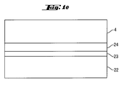
- the transition between multilayer system and protective coating is shown in detail in Figure 1e , i.e., in the present example the transition of uppermost absorber layer 22 and protective layer 4.
- the protective layer may be made of one material or assembled from multiple, i.e., two, three, four, or more layers.
- Preferred materials for the simple or assembled protective layer 4 are, for example, boron carbide, molybdenum boride, boron nitride, silicon nitride, silicon carbide, beryllium oxide, silicon oxide, titanium, titanium nitride, copper gold alloy, nickel, ruthenium, rhodium, iridium, gold, palladium, platinum, osmium, samarium, gadolinium, aluminum oxide, potassium, hafnium, thorium fluoride, natrium fluoride, lithium fluoride, magnesium fluoride, lanthanium fluoride, amorphous carbon, yttrium, niobium, rhodium oxide, ruthenium oxide, cerium, or silicon hydride.
- a first intermediate layer 23 for increasing reflectivity and a second intermediate layer 24 as a barrier and in certain circumstances also for increasing reflectivity are situated between the uppermost absorber layer 22 and the protective layer 4.
- the first intermediate layer 23 is situated between the uppermost absorber layer 22 and the second intermediate layer 24.
- the second intermediate layer 24 may also be situated between the protective layer 4 and the first intermediate layer 23 or also on both sides of the first intermediate layer 23.
- the multilayer system may also terminate with a spacer layer instead of with an absorber layer.
- First and second intermediate layers may then, too, be provided in the way described above at the transition to the protective layer to increase the reflectivity.
- the total thickness of the protective layer 4 is advantageously selected in a range between approximately 1 nm and approximately 10 nm and the total thickness of first and second intermediate layers 23, 24 is selected in a range between approximately 0.2 nm and approximately 10 nm.
- the materials for the first and second intermediate layers 23, 24 at the transition to the protective layer 4 may be identical to those for first and second intermediate layers 23a,b, 24a,b between the absorber and spacer layers 22, 21 or may also deviate therefrom.
- First and second intermediate layers may either be provided at the transition to the protective layer or within the multilayer system or also both at the transition to the protective layer and also within the multilayer system.
- the solid line which corresponds to a real Mo/Si multilayer system, is used as a comparison measure.
- a mixed layer which may be approximately described by Mo 7 Si 3 and typically has a thickness of 8 ⁇ , i.e., 0.8 nm, forms by interdiffusion at the interface between the molybdenum and silicon layers in a real Mo/Li multilayer system. This mixed layer results in a reduction of the maximum reflectivity from just 70% to approximately 69%.
- an intermediate layer made of ruthenium, rhodium, molybdenum carbide, and ruthenium silicide was studied as a function of the layer thickness.
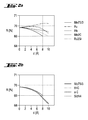
- materials which are suitable for the second intermediate layer are shown in Figure 2b .
- These are boron carbide, amorphous carbon, and silicon nitride, which are all known for being relatively chemically inert to silicon and also acting as a diffusion barrier. They only differ insignificantly at all thicknesses in their effect on the reflectivity and all result in a still acceptable reflectivity reduction in relation to the normal molybdenum-silicon multilayer system.
- silicon carbide is also suitable as a material for the second intermediate layer at the interface molybdenum-on-silicon. It is comparable in its effect on the reflectivity to the materials boron carbide, amorphous carbon, and silicon nitride shown in Figure 2b .
- Boron carbide, amorphous carbon, and silicon nitride were again studied as materials for the second intermediate layer.
- intermediate layers made of amorphous carbon and silicon nitride already have a very negative influence on the reflectivity at very low thicknesses at the interface of silicon on molybdenum (see Figure 3b ), while boron carbide results in a slight increase of the reflectivity in relation to the molybdenum/silicon multilayer system having a genuine molybdenum silicide layer for all studied thicknesses.
- Boron carbide is thus preferred as the material for the second intermediate layer at least at the interface silicon-on-molybdenum.
- At least the material of the first additional layer 23a,b i.e. the reflectivity enhancing layer, has an index of refraction whose value of the real part of the index of refraction at the operating wavelength is either greater than the corresponding value of the alternating material having the higher real part of the index of refraction or is lower than the corresponding value of the alternating material having the lower real part of the index of refraction.
- the optical contrast within the multilayer system is thus increased and thus also the reflectivity.
- ruthenium is suitable as the material of the first additional layer 23a above a silicon layer and below a molybdenum layer, which has a significantly lower real part of the index of refraction at the operating wavelength of 13.5 nm here than molybdenum (see also Table 1).
- the thickness of the first additional layer it is to be ensured that it is not selected as so high that the effect of the reflectivity gain is compensated for because of the higher optical contrast due to the additional absorption because of the first additional layer. This is important in particular with materials having a high imaginary part of the index of refraction at the operating wavelength such as ruthenium (see also Table 1).
- At least the material of the first additional layer has an index of refraction whose value of the real part of the index of refraction at the operating wavelength is between the corresponding values of the alternating materials.
- Such a material does tend to reduce the optical contrast of the multilayer system.
- the standing wave field has a total absorption which is primarily influenced by the overall distribution of the intensities in the various layers in connection with the individual absorptions of the layers because of their particular materials, which are determined by the imaginary part of their indices of refraction.
- the distributions of the intensities shift, so that another total absorption of the standing wave field results.
- the position of the extremes and the nodes are shifted by additional layers made of material whose value of the real part of the index of refraction at the operating wavelength is between the corresponding values of the alternating materials in such a way that the maxima are shifted out of areas made of material having a relatively high imaginary part of the index of refraction, i.e., higher absorption, into areas made of material having a relatively low imaginary part of the index of refraction, i.e., lower absorption.
- the absorption thus reduced results in an increased reflectivity.
- the suitable materials for the additional layers in the suitable thickness range are to be ascertained again for every multilayer system, because too large or too small a shift of the standing wave field may also result in an increase of the total absorption and reduction of the reflectivity.
- yttrium and niobium are particularly suitable as the material for the first additional layer above a molybdenum layer and below a silicon layer.
- Second intermediate layer Materials that are suitable as second intermediate layer, i.e. as barrier layer, often show a low enthalpy of formation with respect to the adjacent material, in the present case the material of the first intermediate layer and the spacer and/or the absorber layer. They often show a low diffusion rate with respect to the adjacent material. Besides, they often show a tendency to grow layers as closed atomic layers in opposite to an insular growth pattern.
- the material of the second intermediate layer has appropriate optical constants at the operating wavelength, as explained before in relation with the material for the first intermediate layer.
- first or second intermediate layers are also suitable for corresponding intermediate layers at the transition to a protective layer.
- the thicknesses of the intermediate layers are preferably less than those of the layers made of the alternating materials which are used as spacer and absorber layers and which define the basic characteristics of the reflective optical element, in particular the operating wavelength range.
- the thickness of the additional layers is especially preferably less than one fourth of the operating wavelength, in particular less than one eighth of the operating wavelength.
- a molybdenum-silicon multilayer system having yttrium as the first intermediate layer 23a at the silicon-on-molybdenum interface and boron carbide as the second intermediate layer 24a toward the silicon layer 21 as well as ruthenium as the first intermediate layer 23b on the molybdenum-on-silicon interface and boron carbide again as the second intermediate layer 24b toward the silicon layer was produced. All layers were applied by electron beam vapor deposition.
- the individual layer thicknesses were approximately 2.8 nm per molybdenum, 0.6 nm for yttrium, 0.2 nm for both boron carbide layers, 4.2 nm for silicon, and 0.8 nm for ruthenium.
- the stack 20 comprising this repeated fifty times.
- An actual achievable percent maximum reflectivity of somewhat above 71% resulted at the operating wavelength of 13.5 nm. This means an increase of more than 2% compared to the 69% which may actually be achieved by a comparable molybdenum-silicon multilayer system without intermediate layer according to the present invention.
- the reflective optical element just described was produced in that the boron carbide intermediate layers were applied not by electron beam vapor deposition, but rather by magnetron sputtering. In this case as well, a maximum percent reflectivity of somewhat over 71% resulted at an operating wavelength of 13.5 nm.
- a further reflective optical element was produced, in which all individual layers were again applied by electron beam vapor deposition.
- Yttrium was replaced here by niobium as the material for the first intermediate layer at the interface silicon on molybdenum.
- a maximum percent reflectivity of approximately 71% was achieved at 13.5 nm by this reflective optical element.
- the reflective optical elements according to the present invention have the further advantage, in addition to their high actually achievable reflectivity, that the structure of their multilayer system also remains stable over longer usage times thanks to the second intermediate layers in particular. This is because the second intermediate layers prevent interdiffusion with the layers adjoining them also under thermal strain by continuous irradiation with EUV or soft x-ray radiation. The maximum reflectivity at the operating wavelength is thus maintained even in continuous operation.
- An EUV lithography device 100 is schematically illustrated in Figure 4 .
- Essential parts are the beam shaping system 110, the illumination system 120, the photomask 130, and the projection system 140.
- a plasma source or also a synchrotron may be used as the radiation source 111.
- the exiting radiation in the wavelength range of approximately 5 nm to 20 nm is first bundled in the collimator 112.
- the desired operating wavelength is filtered out by varying the angle of incidence.
- the collimator 112 and the monochromator 113 are typically implemented as reflective optical elements in the cited wavelength range.
- the use of reflective elements according to the present invention, for example, as the collimator 112 or as the monochromator 113, is advisable particularly in the beam shaping system 110. This is because the thermal strain is especially high here and it is especially important to provide a maximum of EUV radiation by high reflectivity of the following parts.
- the illumination system 120 has two mirrors 121, 122, which both have multilayer systems having first and second intermediate layers as previously explained. It is to be noted that the illumination system 120 may also have only one also three, four, five, or more mirrors, which may all or partially have a multilayer system having first and second intermediate layers as previously explained.
- the mirrors 121, 122 conduct the beam to the photomask 130, which has the structure which is to be imaged on the wafer 150.
- the photomask 130 is also a reflective optical element for the EUV and soft x-ray wavelength range having a multilayer system having first and second intermediate layers.
- the projection system 140 has two mirrors 141, 142 having a multilayer system having first and second intermediate layers in the illustrated example. It is to be noted that the projection system 140 may also have only one or also three, four, five, or more mirrors, one or more mirrors of which may have a multilayer system having first and second intermediate layers.
Landscapes
- Engineering & Computer Science (AREA)
- Physics & Mathematics (AREA)
- Chemical & Material Sciences (AREA)
- Nanotechnology (AREA)
- General Engineering & Computer Science (AREA)
- High Energy & Nuclear Physics (AREA)
- Spectroscopy & Molecular Physics (AREA)
- Mathematical Physics (AREA)
- Theoretical Computer Science (AREA)
- Crystallography & Structural Chemistry (AREA)
- Exposure Of Semiconductors, Excluding Electron Or Ion Beam Exposure (AREA)
- Exposure And Positioning Against Photoresist Photosensitive Materials (AREA)
- Optical Elements Other Than Lenses (AREA)
Description
- The present invention relates to a reflective optical element for an operating wavelength in the extreme ultraviolet and soft x-ray wavelength range, in particular for use in EUV lithography devices, which has a multilayer system made of at least two alternating materials having different real parts of the index of refraction at the operating wavelength.
- Reflective optical elements for the extreme ultraviolet (EUV) and soft x-ray wavelength range (e.g., wavelengths between approximately 1 nm and 20 nm) such as photomasks or multilayer mirrors, are used in particular in the lithography of semiconductor components. Because EUV lithography devices typically have multiple reflective optical elements, they must have the highest possible reflectivity to ensure a sufficiently high total reflectivity. Because typically multiple reflective optical elements are situated one behind another in an EUV lithography device, even small reflectivity losses at each individual reflective optical element have a greater effect on the total reflectivity.
- Reflective optical elements for the EUV and soft x-ray wavelength range typically have multilayer systems. These are alternatingly applied layers of a material having a higher real part of the index of refraction at the operating wavelength (also called a spacer) and a material having a lower real part of the index of refraction at the operating wavelength (also called an absorber), an absorber-spacer pair forming a stack. A crystal is thus simulated in a certain way, whose lattice planes correspond to the absorber layers at which Bragg reflection occurs. The thicknesses of the individual layers and also of the repeating stack may be constant or also vary over the entire multilayer system, depending on which reflection profile is to be achieved.
- One approach for ensuring the highest possible total reflectivities in EUV lithography devices is to provide reflective optical elements with a protective layer, which may comprise one or more layers, to protect the reflective optical elements from contamination. The service life of the reflective optical elements is thus lengthened and a reflectivity loss over time is reduced.
- A further approach comprises supplementing the basic structure made of absorber and spacer with further more and less absorbent materials to increase the maximum possible reflectivity at the particular operating wavelength. For this purpose, in many stacks, absorber and/or spacer materials may be exchanged with one another or the stack may be constructed from more than one absorber and/or spacer material. The absorber and spacer materials may have constant or also varying thicknesses over all stacks to optimize the reflectivity. In practice, higher reflectivities cannot be achieved to the expected extent in reflective optical elements having complex material sequences
KR 20070003521 A - It is an object of the present invention to provide a reflective optical element which provides the highest possible reflectivity at its operating wavelength.
- This object is achieved by a reflective optical element according to independent claim 1.
- Advantageous embodiments are found in the dependent claims.
- The present invention will be explained in greater detail with reference to a preferred exemplary embodiment.
- Figure 1a
- shows a schematic illustration of a reflective optical element;
- Figure 1b
- shows a schematic detail illustration of the reflective optical element;
- Figure 1c
- shows a schematic detail illustration of an embodiment of the reflective optical element;
- Figure 1d
- shows a schematic detail illustration of a further embodiment of the reflective optical element;
- Figure 1e
- shows a further schematic detail illustration of the reflective optical element;
- Figure 2a
- shows the influence on the maximum reflectivity of different materials as the first additional layer on silicon;
- Figure 2b
- shows the influence on the maximum reflectivity of different materials as the second additional layer on silicon;
- Figure 3a
- shows the influence on the maximum reflectivity of different materials as the first additional layer on molybdenum;
- Figure 3b
- shows the influence on the maximum reflectivity of different materials as the second additional layer on molybdenum; and
- Figure 4
- shows a schematic illustration of an EUV lithography device.
-
Figures 1a,b show an example of a reflective optical element 1 for the extreme ultraviolet and soft x-ray wavelength range, in particular for use in EUV lithography devices, e.g., as a photomask or as a mirror.Figure 1a schematically shows the higher-order structure of themultilayer system 2. Themultilayer system 2 has been produced in the present example by successively coating asubstrate 3 using different materials having different complex indices of refraction. Moreover, aprotective layer 4 was additionally applied to themultilayer system 2 for protection from external influences such as contamination. Theprotective layer 4 itself may be composed of multiple different material layers, which are inert to various contamination influences, suppress a chemical interaction with themultilayer system 2, and ensure an optical adaptation to themultilayer system 2, for example, to influence the optical properties such as the reflectivity of the reflective optical system 1 as little as possible. - The
multilayer system 2 essentially comprises multiple repeatingstacks 20, whose structure is schematically shown inFigure 1 b. The essential layers of astack 20, which particularly result in reflection at an operating wavelength due to the multiple repetition of thestacks 20, are the so-calledabsorber layers 22 made of a material having a lower real part of the index of refraction and the so-calledspacer layers 21 made of a material having a higher real part of the index of refraction. Thus, a crystal is in a way simulated, theabsorber layers 22 corresponding to the lattice planes within the crystal, which have a distance to one another defined by theparticular spacer layers 21 and at which reflection of incident EUV and/or soft x-ray radiation occurs. The thicknesses of the layers are selected in such a way that at a specific operating wavelength, the radiation reflected at eachabsorber layer 22 constructively superimposes, to thus achieve maximum reflectivity of the reflective optical element. In the present example illustrated inFigure 1b , a firstintermediate layer 23a,b to increase the maximum reflectivity in relation to the basic reflectivity, which would result if only thespacer layers 21 and theabsorber layers 22 were provided, i.e. the theoretically maximum possible reflectivity of thestack 20 is increased, is provided both at the interface betweenabsorber layer 22 onspacer layer 21 and also at the interface betweenspacer layer 21 onabsorber layer 22. As well, a secondintermediate layer 24a,b is provided, which acts as a barrier between the firstintermediate layer 23a,b and, in the present example, of theadjoining spacer layer 21 against chemical interaction or diffusion, advantageously against both. - It is to be noted that it is also possible to provide the two
intermediate layers 23a,b, 24a,b at only one of the two interfaces betweenabsorber layer 22 andspacer layer 21 or betweenspacer layer 21 andabsorber layer 22. However, such arrangements are not covered by the scope of the present invention. - It is also possible to provide two second
intermediate layers 24a,b on both sides of the firstintermediate layer 23a,b to thus suppress a chemical interaction and/or diffusion both with thespacer layer 21 and also with theabsorber layer 22, as is schematically illustrated inFig. 1c , wherein the secondintermediate layers intermediate layer absorber layer 22 to provide the secondintermediate layer 24a,b. A further possibility consists in having alternatingly the first intermediate layer on the absorber layer and the second intermediate layer on the spacer layer and vice-versa, as is schematically illustrated inFig. 1d , thus inverting the sequence of the two additional layers depending on the transition being from absorber to spacer or from spacer to absorber layer. In particular, it is also possible to select different materials for the intermediate layers, depending on whether the intermediate layers are to be situated betweenabsorber layer 22 andspacer layer 21 or betweenspacer layer 21 and absorberlayer 22 leading to different intermediate layers, e.g. 23 a and 23b or 24a and 24b, respectively. For each type of intermediate layer, more than two different materials can be chosen, in particular in stacks comprising more than two absorber layers and/or spacer layers. Preferably, the intermediate layers have a different thickness depending on the transition being from absorber to spacer or from spacer to absorber layer. - The transition between multilayer system and protective coating is shown in detail in
Figure 1e , i.e., in the present example the transition ofuppermost absorber layer 22 andprotective layer 4. As already explained, the protective layer may be made of one material or assembled from multiple, i.e., two, three, four, or more layers. Preferred materials for the simple or assembledprotective layer 4 are, for example, boron carbide, molybdenum boride, boron nitride, silicon nitride, silicon carbide, beryllium oxide, silicon oxide, titanium, titanium nitride, copper gold alloy, nickel, ruthenium, rhodium, iridium, gold, palladium, platinum, osmium, samarium, gadolinium, aluminum oxide, potassium, hafnium, thorium fluoride, natrium fluoride, lithium fluoride, magnesium fluoride, lanthanium fluoride, amorphous carbon, yttrium, niobium, rhodium oxide, ruthenium oxide, cerium, or silicon hydride. In the present example, a firstintermediate layer 23 for increasing reflectivity and a secondintermediate layer 24 as a barrier and in certain circumstances also for increasing reflectivity are situated between theuppermost absorber layer 22 and theprotective layer 4. In the example shown inFigure 1e , the firstintermediate layer 23 is situated between theuppermost absorber layer 22 and the secondintermediate layer 24. As needed, the secondintermediate layer 24 may also be situated between theprotective layer 4 and the firstintermediate layer 23 or also on both sides of the firstintermediate layer 23. Moreover, the multilayer system may also terminate with a spacer layer instead of with an absorber layer. First and second intermediate layers may then, too, be provided in the way described above at the transition to the protective layer to increase the reflectivity. In the dimensioning of theintermediate layers protective layer 4, the total thickness of theprotective layer 4 is advantageously selected in a range between approximately 1 nm and approximately 10 nm and the total thickness of first and secondintermediate layers intermediate layers protective layer 4 may be identical to those for first and secondintermediate layers 23a,b, 24a,b between the absorber and spacer layers 22, 21 or may also deviate therefrom. First and second intermediate layers may either be provided at the transition to the protective layer or within the multilayer system or also both at the transition to the protective layer and also within the multilayer system. - Some examples will be further explained on the basis of a stack with the materials molybdenum as absorber and silicon as spacer, which are often used in the EUV and soft x-ray wavelength range. The following statements may also be transferred similarly to other suitable multilayer systems for the EUV and soft x-ray wavelength range, such as molybdenum/beryllium, molybdenum carbide/silicon, or ruthenium/silicon. They may also be transferred to multilayer systems which are based on alternating layers made of more than two materials. Furthermore, it is to be noted that the at least two intermediate layers may be used in multilayer systems having both constant and also varying thickness ratios of the individual layers within a stack.
- Firstly, the interface of molybdenum on silicon will be examined in greater detail. The thickness dependency of the reflectivity of some possible materials for the first intermediate layer on silicon, i.e. the reflectivy enhancing layer, is shown in
Figure 2a , the thickness dependency of the reflectivity of some possible materials for the second intermediate layer on silicon, i.e. the barrier layer, is shown inFigure 2b . - The solid line, which corresponds to a real Mo/Si multilayer system, is used as a comparison measure. A mixed layer, which may be approximately described by Mo7Si3 and typically has a thickness of 8 Å, i.e., 0.8 nm, forms by interdiffusion at the interface between the molybdenum and silicon layers in a real Mo/Li multilayer system. This mixed layer results in a reduction of the maximum reflectivity from just 70% to approximately 69%. In contrast, firstly the influence on the reflectivity of adding an intermediate layer made of ruthenium, rhodium, molybdenum carbide, and ruthenium silicide was studied as a function of the layer thickness. As may be seen from
Figure 2a , with increasing thickness, the reflectivity decreases with an intermediate layer made of molybdenum carbide or ruthenium silicide, but not a strongly as with the genuinely forming intermediate layer made of molybdenum silicide. With rhodium, a slight reflectivity increase may be seen at a thickness of up to approximately 6 Å, but the reflectivity sinks even more strongly at higher thicknesses. An astounding effect may be seen with ruthenium: up to a thickness of 8 Å, the reflectivity increases to above 70%, to then remain constant up to at least 10 A. All of the materials shown here are fundamentally suitable as a material for the first intermediate layer, because they result in a real reflectivity gain in relation to the pure molybdenum-silicon multilayer system. Ruthenium is especially preferred as the material for the first intermediate layer. - Correspondingly, materials which are suitable for the second intermediate layer are shown in
Figure 2b . These are boron carbide, amorphous carbon, and silicon nitride, which are all known for being relatively chemically inert to silicon and also acting as a diffusion barrier. They only differ insignificantly at all thicknesses in their effect on the reflectivity and all result in a still acceptable reflectivity reduction in relation to the normal molybdenum-silicon multilayer system. It is to be noted that silicon carbide is also suitable as a material for the second intermediate layer at the interface molybdenum-on-silicon. It is comparable in its effect on the reflectivity to the materials boron carbide, amorphous carbon, and silicon nitride shown inFigure 2b . - For the interface silicon-on-molybdenum, it has been found that different materials suggest themselves for the reflectivity increase than for the interface molybdenum-on-silicon. In particular yttrium, niobium, niobium silicide, and yttrium silicide were studied in regard to their influence on the maximum reflectivity at the interface silicon on molybdenum. The results are shown in
Figure 3a . All four materials first display an increase of the reflectivity up to maximum of 70% or more and then a drop of the reflectivity. The maximum is already at 4 A for yttrium silicide, and approximately 6 A for niobium and niobium silicide, and only shortly before 8 A for yttrium. The maximum reflectivity is also above 70% at 10 A. Therefore yttrium is especially preferred as the material for the first intermediate layer. - Boron carbide, amorphous carbon, and silicon nitride were again studied as materials for the second intermediate layer. In contrast to the interface of molybdenum on silicon, intermediate layers made of amorphous carbon and silicon nitride already have a very negative influence on the reflectivity at very low thicknesses at the interface of silicon on molybdenum (see
Figure 3b ), while boron carbide results in a slight increase of the reflectivity in relation to the molybdenum/silicon multilayer system having a genuine molybdenum silicide layer for all studied thicknesses. Boron carbide is thus preferred as the material for the second intermediate layer at least at the interface silicon-on-molybdenum. - Upon more precise observation of the properties of the materials which result in an increase of the maximum relative reflectivity of a multilayer system at an operating wavelength in the EUV and/or soft x-ray wavelength range in relation to a multilayer system without intermediate layers, e.g. a molybdenum/silicon multilayer system, one establishes two variants in particular. This is true in particular for the intermediate layer materials which result in a rise of the reflectivity not only in relation to a real molybdenum/silicon multilayer system having a mixed layer, but rather also in relation to an ideal molybdenum/silicon multilayer system (corresponds to the reflectivity at d = 0 A in
Figures 2a,b ,3a,b ). - In a first variant, at least the material of the first
additional layer 23a,b, i.e. the reflectivity enhancing layer, has an index of refraction whose value of the real part of the index of refraction at the operating wavelength is either greater than the corresponding value of the alternating material having the higher real part of the index of refraction or is lower than the corresponding value of the alternating material having the lower real part of the index of refraction. The optical contrast within the multilayer system is thus increased and thus also the reflectivity. For example, in the case observed here of a molybdenum/silicon multilayer system, ruthenium is suitable as the material of the firstadditional layer 23a above a silicon layer and below a molybdenum layer, which has a significantly lower real part of the index of refraction at the operating wavelength of 13.5 nm here than molybdenum (see also Table 1). For the selection of the thickness of the first additional layer it is to be ensured that it is not selected as so high that the effect of the reflectivity gain is compensated for because of the higher optical contrast due to the additional absorption because of the first additional layer. This is important in particular with materials having a high imaginary part of the index of refraction at the operating wavelength such as ruthenium (see also Table 1). - In a second variant, at least the material of the first additional layer has an index of refraction whose value of the real part of the index of refraction at the operating wavelength is between the corresponding values of the alternating materials. Such a material does tend to reduce the optical contrast of the multilayer system. However, it results in a shift of the standing wave of the electrical field which forms upon irradiation of the multilayer system by refraction at the individual layer boundaries and interference. The standing wave field has a total absorption which is primarily influenced by the overall distribution of the intensities in the various layers in connection with the individual absorptions of the layers because of their particular materials, which are determined by the imaginary part of their indices of refraction. By incorporating the additional layer, the distributions of the intensities shift, so that another total absorption of the standing wave field results. As a special case, the position of the extremes and the nodes are shifted by additional layers made of material whose value of the real part of the index of refraction at the operating wavelength is between the corresponding values of the alternating materials in such a way that the maxima are shifted out of areas made of material having a relatively high imaginary part of the index of refraction, i.e., higher absorption, into areas made of material having a relatively low imaginary part of the index of refraction, i.e., lower absorption. The absorption thus reduced results in an increased reflectivity. It is to be noted that the suitable materials for the additional layers in the suitable thickness range are to be ascertained again for every multilayer system, because too large or too small a shift of the standing wave field may also result in an increase of the total absorption and reduction of the reflectivity. In the example described here of a molybdenum/silicon multilayer system, for example, yttrium and niobium are particularly suitable as the material for the first additional layer above a molybdenum layer and below a silicon layer.
- Materials that are suitable as second intermediate layer, i.e. as barrier layer, often show a low enthalpy of formation with respect to the adjacent material, in the present case the material of the first intermediate layer and the spacer and/or the absorber layer. They often show a low diffusion rate with respect to the adjacent material. Besides, they often show a tendency to grow layers as closed atomic layers in opposite to an insular growth pattern. Preferably, the material of the second intermediate layer has appropriate optical constants at the operating wavelength, as explained before in relation with the material for the frist intermediate layer.
- It is to be noted that the materials cited in regard to the present example for the first or second intermediate layers are also suitable for corresponding intermediate layers at the transition to a protective layer.
- The thicknesses of the intermediate layers are preferably less than those of the layers made of the alternating materials which are used as spacer and absorber layers and which define the basic characteristics of the reflective optical element, in particular the operating wavelength range. The thickness of the additional layers is especially preferably less than one fourth of the operating wavelength, in particular less than one eighth of the operating wavelength.
- For example, for an operating wavelength of 13.5 nm, a molybdenum-silicon multilayer system having yttrium as the first
intermediate layer 23a at the silicon-on-molybdenum interface and boron carbide as the secondintermediate layer 24a toward thesilicon layer 21 as well as ruthenium as the firstintermediate layer 23b on the molybdenum-on-silicon interface and boron carbide again as the secondintermediate layer 24b toward the silicon layer was produced. All layers were applied by electron beam vapor deposition. The individual layer thicknesses were approximately 2.8 nm per molybdenum, 0.6 nm for yttrium, 0.2 nm for both boron carbide layers, 4.2 nm for silicon, and 0.8 nm for ruthenium. Thestack 20 comprising this repeated fifty times. An actual achievable percent maximum reflectivity of somewhat above 71% resulted at the operating wavelength of 13.5 nm. This means an increase of more than 2% compared to the 69% which may actually be achieved by a comparable molybdenum-silicon multilayer system without intermediate layer according to the present invention. - For a further example, the reflective optical element just described was produced in that the boron carbide intermediate layers were applied not by electron beam vapor deposition, but rather by magnetron sputtering. In this case as well, a maximum percent reflectivity of somewhat over 71% resulted at an operating wavelength of 13.5 nm.
- In addition, a further reflective optical element was produced, in which all individual layers were again applied by electron beam vapor deposition. Yttrium was replaced here by niobium as the material for the first intermediate layer at the interface silicon on molybdenum. A maximum percent reflectivity of approximately 71% was achieved at 13.5 nm by this reflective optical element.
- The reflective optical elements according to the present invention have the further advantage, in addition to their high actually achievable reflectivity, that the structure of their multilayer system also remains stable over longer usage times thanks to the second intermediate layers in particular. This is because the second intermediate layers prevent interdiffusion with the layers adjoining them also under thermal strain by continuous irradiation with EUV or soft x-ray radiation. The maximum reflectivity at the operating wavelength is thus maintained even in continuous operation. This makes the reflective optical element according to the present invention particularly suitable for use in EUV lithography devices, in which they may be used at diverse places as mirror elements or mask elements, for example.
- An
EUV lithography device 100 is schematically illustrated inFigure 4 . Essential parts are thebeam shaping system 110, theillumination system 120, thephotomask 130, and theprojection system 140. - For example, a plasma source or also a synchrotron may be used as the
radiation source 111. The exiting radiation in the wavelength range of approximately 5 nm to 20 nm is first bundled in thecollimator 112. In addition, with the aid of amonochromator 113, the desired operating wavelength is filtered out by varying the angle of incidence. Thecollimator 112 and themonochromator 113 are typically implemented as reflective optical elements in the cited wavelength range. The use of reflective elements according to the present invention, for example, as thecollimator 112 or as themonochromator 113, is advisable particularly in thebeam shaping system 110. This is because the thermal strain is especially high here and it is especially important to provide a maximum of EUV radiation by high reflectivity of the following parts. - The operating beam, which is prepared in regard to wavelength and spatial distribution in the
beam shaping system 110, is then introduced into theillumination system 120. In the example shown inFigure 4 , theillumination system 120 has twomirrors illumination system 120 may also have only one also three, four, five, or more mirrors, which may all or partially have a multilayer system having first and second intermediate layers as previously explained. - The
mirrors photomask 130, which has the structure which is to be imaged on thewafer 150. Thephotomask 130 is also a reflective optical element for the EUV and soft x-ray wavelength range having a multilayer system having first and second intermediate layers. - With the aid of the
projection system 140, the beam reflected by thephotomask 130 is projected on thewafer 150 and the structure of thephotomask 130 is thus imaged thereon. Theprojection system 140 has twomirrors projection system 140 may also have only one or also three, four, five, or more mirrors, one or more mirrors of which may have a multilayer system having first and second intermediate layers. -
- 1
- reflective optical element
- 2
- multilayer system
- 3
- substrate
- 4
- protective layer
- 20
- periodically repeating layer stack
- 21
- material having low absorption coefficient
- 22
- material having high absorption coefficient
- 23, 23a,b
- first intermediate layer to increase reflectivity
- 24, 24a,b, 24a',b'
- second intermediate layer as a diffusion barrier
- 100
- EUV lithography device
- 110
- beam shaping system
- 111
- light source
- 112
- collimator
- 113
- monochromator
- 120
- illumination system
- 121, 122
- mirror
- 130
- mask
- 140
- projection system
- 141, 142
- mirror
- 150
- wafer
- R
- maximum reflectivity
- d
- thickness
| Index of refraction at a wavelength of 13.5 nm | ||
| Name | Real part | |
| Mo | ||
| 0,923793525 | 0,006435425 | |
| |
0,917767145 | 0, |
| Ru | ||
| 0,886360034 | 0,017064894 | |
| |
0,875048831 | 0,031177852 |
| |
0,899574861 | 0,016169887 |
| |
0,999002305 | 0,001826494 |
| |
0,973729959 | 0,002281516 |
| |
0,933749691 | 0,005195933 |
| |
0,938146889 | 0,005302884 |
| |
0,977611721 | 0,002474689 |
| |
0,963771485 | 0,005145842 |
| |
0,961573470 | 0,006905315 |
| |
0,973136209 | 0,009317771 |
| |
0,926676892 | 0,006498690 |
Claims (10)
- A reflective optical element arranged for an operating wavelength in the soft x-ray and extreme ultraviolet wavelength range between 1 nm and 20 nm, in particular for use in an EUV lithography device, which has a multilayer system (2) made of at least two alternating materials having different real parts of the index of refraction at the operating wavelength, wherein at both of two neighboring interfaces between these two alternating materials (21, 22) two additional layers (23a,b, 24a,b, 24a',b') of different further materials are situated such as to adjoin at least one of the two alternating materials (21, 22), one of the two neighboring interfaces being an interface from the material (22) having a lower real part of the index of refraction to the material (21) having a higher real part of the index of refraction and the other of the two neighboring interfaces being an interface from the material (21) having a higher real part of the index of refraction to the material (22) having a lower real part of the index of refraction, and wherein the two additional layers (23a,b, 24a,b, 24a',b') are chosen differently at both interfaces.
- The reflective optical element according to Claim 1, characterized in that the sequence of the two additional layers (23a,b, 24a,b) is chosen differently at both interfaces.
- The reflective optical element according to Claim 1 or 2, characterized in that the material of at least one of the two additional layers (23a,b, 24a,b, 24a',b') is chosen differently at both interfaces.
- The reflective optical element according to one of Claims 1 through 3, characterized in that a first additional layer (23a,b) of the two additional layers is situated on at least one of the two neighboring interfaces between the two alternating materials (21, 22), which results in an increase of the maximum reflectivity of the multilayer system (2) at the operating wavelength in comparison to the reflectivity without the additional layer, and a second additional layer (24a,b, 24a',b') of the two additional layers is situated at the same interface between the two alternating materials (21, 22), which acts as a barrier between the adjoining layers.
- The reflective optical element according to one of Claims 1 through 4, characterized in that the first additional layer (23a,b) comprises a material from the group consisting of ruthenium, rhodium, yttrium, and niobium.
- The reflective optical element according to one of Claims 1 through 5, characterized in that at least the material of the first additional layer (23a,b) has an index of refraction whose value of the real part of the index of refraction at the operating wavelength is either greater than the corresponding value of the alternating material (21) having the higher real part of the index of refraction or is lower than the corresponding value of the alternating material (22) having the lower real part of the index of refraction.
- The reflective optical element according to one of Claims 1 through 5, characterized in that at least the material of the first additional layer (23a,b) has an index of refraction whose value of the real part of the index of refraction at the operating wavelength is between the corresponding values of the alternating materials (21, 22).
- The reflective optical element according to one of Claims 1 through 7, characterized in that the thickness (d) of each of the additional layers (23, 23a,b, 24, 24a,b, 24a',b') is less than that of each of the layers (21, 22) made of the alternating materials.
- The reflective optical element according to one of Claims 1 through 8, characterized in that the material (22) having a lower real part of the index of refraction at the operating wavelength is molybdenum and the material (21) having a higher real part of the index of refraction at the operating wavelength is silicon
- The reflective optical element according to one of Claims 1 through 9, characterized in that the second additional layer (24a,b, 24a',b') comprises boron carbide.
Applications Claiming Priority (3)
| Application Number | Priority Date | Filing Date | Title |
|---|---|---|---|
| US88814407P | 2007-02-05 | 2007-02-05 | |
| DE102007006423 | 2007-02-05 | ||
| PCT/EP2008/000842 WO2008095663A1 (en) | 2007-02-05 | 2008-02-02 | Multilayer reflective optical element for euv lithography devices comprising first and second additional intermediate layers |
Publications (2)
| Publication Number | Publication Date |
|---|---|
| EP2115751A1 EP2115751A1 (en) | 2009-11-11 |
| EP2115751B1 true EP2115751B1 (en) | 2015-05-27 |
Family
ID=39587554
Family Applications (1)
| Application Number | Title | Priority Date | Filing Date |
|---|---|---|---|
| EP08715682.4A Not-in-force EP2115751B1 (en) | 2007-02-05 | 2008-02-02 | Multilayer reflective optical element for euv lithography devices comprising first and second additional intermediate layers |
Country Status (7)
| Country | Link |
|---|---|
| US (1) | US8144830B2 (en) |
| EP (1) | EP2115751B1 (en) |
| JP (2) | JP2010518594A (en) |
| KR (1) | KR101490533B1 (en) |
| DE (1) | DE102008007387A1 (en) |
| TW (1) | TWI427334B (en) |
| WO (1) | WO2008095663A1 (en) |
Families Citing this family (52)
| Publication number | Priority date | Publication date | Assignee | Title |
|---|---|---|---|---|
| TWI427334B (en) * | 2007-02-05 | 2014-02-21 | Zeiss Carl Smt Gmbh | Reflective optical element for euv lithography devices |
| DE102008040265A1 (en) | 2008-07-09 | 2010-01-14 | Carl Zeiss Smt Ag | Reflective optical element and method for its production |
| US20100271693A1 (en) * | 2009-04-24 | 2010-10-28 | Manuela Vidal Dasilva | Narrowband filters for the extreme ultraviolet |
| US8369674B2 (en) * | 2009-05-20 | 2013-02-05 | General Electric Company | Optimizing total internal reflection multilayer optics through material selection |
| DE102009043824A1 (en) * | 2009-08-21 | 2011-02-24 | Asml Netherlands B.V. | Reflective optical element and method for its production |
| DE102009045170A1 (en) * | 2009-09-30 | 2011-04-07 | Carl Zeiss Smt Gmbh | Reflective optical element and method for operating an EUV lithography device |
| DE102011075579A1 (en) * | 2011-05-10 | 2012-11-15 | Carl Zeiss Smt Gmbh | Mirror and projection exposure apparatus for microlithography with such a mirror |
| JP2012222349A (en) * | 2011-04-05 | 2012-11-12 | Asml Netherlands Bv | Multilayer mirror and lithographic apparatus |
| DE102011076011A1 (en) * | 2011-05-18 | 2012-11-22 | Carl Zeiss Smt Gmbh | Reflective optical element and optical system for EUV lithography |
| WO2012171674A1 (en) * | 2011-06-15 | 2012-12-20 | Asml Netherlands B.V. | Multilayer mirror, method of producing a multilayer mirror and lithographic apparatus |
| DE102011077983A1 (en) * | 2011-06-22 | 2012-12-27 | Carl Zeiss Smt Gmbh | Method for producing a reflective optical element for EUV lithography |
| JP2014007370A (en) * | 2012-06-01 | 2014-01-16 | Tokyo Electron Ltd | Plasma etching method |
| DE102012221186A1 (en) * | 2012-11-20 | 2013-10-17 | Carl Zeiss Smt Gmbh | Reflective optical element for extreme UV and soft X-ray wavelength region, has several layers serving as diffusion barrier intermediate layer, between which material with lower real portion of refractive index is arranged |
| US9612521B2 (en) * | 2013-03-12 | 2017-04-04 | Applied Materials, Inc. | Amorphous layer extreme ultraviolet lithography blank, and manufacturing and lithography systems therefor |
| DE102013207751A1 (en) * | 2013-04-29 | 2014-10-30 | Carl Zeiss Smt Gmbh | Optical element with a multilayer coating and optical arrangement with it |
| EP2998980A4 (en) | 2013-05-09 | 2016-11-16 | Nikon Corp | OPTICAL ELEMENT, OPTICAL PROJECTION SYSTEM, EXPOSURE APPARATUS, AND DEVICE MANUFACTURING METHOD |
| DE102013222330A1 (en) | 2013-11-04 | 2015-05-07 | Carl Zeiss Smt Gmbh | Mirror, in particular for a microlithographic projection exposure apparatus |
| KR101567057B1 (en) * | 2013-11-15 | 2015-11-09 | 주식회사 에스앤에스텍 | Blankmask for Extreme Ultra-Violet Lithography and Photomask using the same |
| US9739913B2 (en) * | 2014-07-11 | 2017-08-22 | Applied Materials, Inc. | Extreme ultraviolet capping layer and method of manufacturing and lithography thereof |
| US9690016B2 (en) * | 2014-07-11 | 2017-06-27 | Applied Materials, Inc. | Extreme ultraviolet reflective element with amorphous layers and method of manufacturing thereof |
| US9581890B2 (en) * | 2014-07-11 | 2017-02-28 | Applied Materials, Inc. | Extreme ultraviolet reflective element with multilayer stack and method of manufacturing thereof |
| TWI730139B (en) | 2016-07-27 | 2021-06-11 | 美商應用材料股份有限公司 | Extreme ultraviolet mask blank with multilayer absorber and method of manufacture |
| US11275300B2 (en) | 2018-07-06 | 2022-03-15 | Applied Materials Inc. | Extreme ultraviolet mask blank defect reduction |
| US20200051793A1 (en) | 2018-08-13 | 2020-02-13 | Skc Solmics Co., Ltd. | Ring-shaped element for etcher and method for etching substrate using the same |
| KR20200019069A (en) * | 2018-08-13 | 2020-02-21 | 에스케이씨솔믹스 주식회사 | Ring type component for etching apparatus and method for etching substrate with the same |
| TW202026770A (en) | 2018-10-26 | 2020-07-16 | 美商應用材料股份有限公司 | Ta-cu alloy material for extreme ultraviolet mask absorber |
| TWI845579B (en) | 2018-12-21 | 2024-06-21 | 美商應用材料股份有限公司 | Extreme ultraviolet mask absorber and processes for manufacture |
| TWI828843B (en) | 2019-01-31 | 2024-01-11 | 美商應用材料股份有限公司 | Extreme ultraviolet (euv) mask blanks and methods of manufacturing the same |
| US11249390B2 (en) | 2019-01-31 | 2022-02-15 | Applied Materials, Inc. | Extreme ultraviolet mask absorber materials |
| TW202035792A (en) | 2019-01-31 | 2020-10-01 | 美商應用材料股份有限公司 | Extreme ultraviolet mask absorber materials |
| TWI818151B (en) | 2019-03-01 | 2023-10-11 | 美商應用材料股份有限公司 | Physical vapor deposition chamber and method of operation thereof |
| TWI845648B (en) | 2019-04-19 | 2024-06-21 | 美商應用材料股份有限公司 | Bragg reflector, extreme ultraviolet (euv) mask blank comprising the same, and method of manufacturing the same |
| TWI845677B (en) | 2019-05-22 | 2024-06-21 | 美商應用材料股份有限公司 | Extreme ultraviolet mask absorber materials |
| TW202104666A (en) | 2019-05-22 | 2021-02-01 | 美商應用材料股份有限公司 | Extreme ultraviolet mask absorber materials |
| TWI836073B (en) | 2019-05-22 | 2024-03-21 | 美商應用材料股份有限公司 | Extreme ultraviolet (euv) mask blank and method of manufacturing the same |
| TW202104667A (en) | 2019-05-22 | 2021-02-01 | 美商應用材料股份有限公司 | Extreme ultraviolet mask absorber materials |
| TWI836072B (en) | 2019-05-22 | 2024-03-21 | 美商應用材料股份有限公司 | Extreme ultraviolet mask with embedded absorber layer |
| US11385536B2 (en) | 2019-08-08 | 2022-07-12 | Applied Materials, Inc. | EUV mask blanks and methods of manufacture |
| TW202122909A (en) | 2019-10-25 | 2021-06-16 | 美商應用材料股份有限公司 | Extreme ultraviolet mask blank defect reduction methods |
| US11630385B2 (en) | 2020-01-24 | 2023-04-18 | Applied Materials, Inc. | Extreme ultraviolet mask absorber materials |
| TW202129401A (en) | 2020-01-27 | 2021-08-01 | 美商應用材料股份有限公司 | Extreme ultraviolet mask blank hard mask materials |
| TW202131087A (en) | 2020-01-27 | 2021-08-16 | 美商應用材料股份有限公司 | Extreme ultraviolet mask absorber materials |
| TWI817073B (en) | 2020-01-27 | 2023-10-01 | 美商應用材料股份有限公司 | Extreme ultraviolet mask blank hard mask materials |
| TW202141165A (en) | 2020-03-27 | 2021-11-01 | 美商應用材料股份有限公司 | Extreme ultraviolet mask absorber materials |
| TWI836207B (en) | 2020-04-17 | 2024-03-21 | 美商應用材料股份有限公司 | Extreme ultraviolet mask absorber materials |
| US11300871B2 (en) | 2020-04-29 | 2022-04-12 | Applied Materials, Inc. | Extreme ultraviolet mask absorber materials |
| TW202202641A (en) | 2020-07-13 | 2022-01-16 | 美商應用材料股份有限公司 | Extreme ultraviolet mask absorber materials |
| US11609490B2 (en) | 2020-10-06 | 2023-03-21 | Applied Materials, Inc. | Extreme ultraviolet mask absorber materials |
| US20230418148A1 (en) * | 2020-12-25 | 2023-12-28 | Hoya Corporation | Multilayer reflective film-equipped substrate, reflective mask blank, reflective mask, and method for producing semiconductor device |
| US11513437B2 (en) | 2021-01-11 | 2022-11-29 | Applied Materials, Inc. | Extreme ultraviolet mask absorber materials |
| US11592738B2 (en) | 2021-01-28 | 2023-02-28 | Applied Materials, Inc. | Extreme ultraviolet mask absorber materials |
| CN116165848B (en) * | 2022-09-08 | 2026-04-21 | 苏州江泓电子科技有限公司 | A multilayer film material, an extreme ultraviolet light reflector, its preparation method and application |
Family Cites Families (24)
| Publication number | Priority date | Publication date | Assignee | Title |
|---|---|---|---|---|
| JP2723955B2 (en) * | 1989-03-16 | 1998-03-09 | キヤノン株式会社 | Multilayer reflector for soft X-ray and vacuum ultraviolet |
| US6295164B1 (en) * | 1998-09-08 | 2001-09-25 | Nikon Corporation | Multi-layered mirror |
| TWI267704B (en) * | 1999-07-02 | 2006-12-01 | Asml Netherlands Bv | Capping layer for EUV optical elements |
| DE10016008A1 (en) * | 2000-03-31 | 2001-10-11 | Zeiss Carl | Village system and its manufacture |
| US7261957B2 (en) * | 2000-03-31 | 2007-08-28 | Carl Zeiss Smt Ag | Multilayer system with protecting layer system and production method |
| US6396900B1 (en) | 2001-05-01 | 2002-05-28 | The Regents Of The University Of California | Multilayer films with sharp, stable interfaces for use in EUV and soft X-ray application |
| US20030008148A1 (en) * | 2001-07-03 | 2003-01-09 | Sasa Bajt | Optimized capping layers for EUV multilayers |
| JP4460284B2 (en) * | 2001-07-03 | 2010-05-12 | イーユーヴィー リミテッド ライアビリティー コーポレイション | Optical element and method for forming the same |
| JP2003303756A (en) * | 2002-04-09 | 2003-10-24 | Sony Corp | Ultraviolet light reflector |
| EP1394815B1 (en) | 2002-08-28 | 2011-06-22 | ASML Netherlands B.V. | Lithographic apparatus comprising a Mo/Si-multilayer with capping layer |
| US6763086B2 (en) | 2002-09-05 | 2004-07-13 | Osmic, Inc. | Method and apparatus for detecting boron in x-ray fluorescence spectroscopy |
| DE10258709A1 (en) * | 2002-12-12 | 2004-07-01 | Carl Zeiss Smt Ag | Protection system for reflective optical elements, reflective optical element and method for their production |
| JP2005099571A (en) * | 2003-09-26 | 2005-04-14 | Nikon Corp | Multilayer reflector, reflective multilayer film forming method, film forming apparatus, and exposure apparatus |
| DE10360540B4 (en) | 2003-12-22 | 2008-04-17 | Fraunhofer-Gesellschaft zur Förderung der angewandten Forschung e.V. | Reflective layer sequence with barrier layers and their use |
| US7193228B2 (en) * | 2004-03-10 | 2007-03-20 | Cymer, Inc. | EUV light source optical elements |
| JP4566791B2 (en) * | 2004-03-26 | 2010-10-20 | キヤノン株式会社 | Soft X-ray multilayer reflector |
| US7282307B2 (en) * | 2004-06-18 | 2007-10-16 | Freescale Semiconductor, Inc. | Reflective mask useful for transferring a pattern using extreme ultra violet (EUV) radiation and method of making the same |
| JP2006162362A (en) * | 2004-12-06 | 2006-06-22 | Canon Inc | Reflective member with multilayer film |
| JP2006283054A (en) * | 2005-03-31 | 2006-10-19 | Hoya Corp | Sputtering target, manufacturing method for substrate with multi-layered reflecting film, manufacturing method for reflection type mask blank, and manufacturing method for reflection type mask |
| JP2006308483A (en) * | 2005-04-28 | 2006-11-09 | Canon Inc | Multilayer film and method for producing multilayer film |
| KR20070003521A (en) * | 2005-06-30 | 2007-01-05 | 주식회사 하이닉스반도체 | Multilayer Mask for EV |
| JP2007198782A (en) * | 2006-01-24 | 2007-08-09 | Nikon Corp | Multilayer reflector and exposure apparatus |
| TWI427334B (en) * | 2007-02-05 | 2014-02-21 | Zeiss Carl Smt Gmbh | Reflective optical element for euv lithography devices |
| US7848483B2 (en) * | 2008-03-07 | 2010-12-07 | Rigaku Innovative Technologies | Magnesium silicide-based multilayer x-ray fluorescence analyzers |
-
2008
- 2008-01-11 TW TW097101266A patent/TWI427334B/en not_active IP Right Cessation
- 2008-02-01 DE DE102008007387A patent/DE102008007387A1/en not_active Withdrawn
- 2008-02-02 KR KR1020097013784A patent/KR101490533B1/en not_active Expired - Fee Related
- 2008-02-02 JP JP2009547611A patent/JP2010518594A/en active Pending
- 2008-02-02 EP EP08715682.4A patent/EP2115751B1/en not_active Not-in-force
- 2008-02-02 WO PCT/EP2008/000842 patent/WO2008095663A1/en not_active Ceased
-
2009
- 2009-08-05 US US12/536,251 patent/US8144830B2/en not_active Expired - Fee Related
-
2013
- 2013-06-12 JP JP2013123759A patent/JP5508577B2/en active Active
Also Published As
| Publication number | Publication date |
|---|---|
| JP2010518594A (en) | 2010-05-27 |
| US8144830B2 (en) | 2012-03-27 |
| JP5508577B2 (en) | 2014-06-04 |
| TW200835943A (en) | 2008-09-01 |
| DE102008007387A1 (en) | 2008-08-07 |
| WO2008095663A1 (en) | 2008-08-14 |
| KR20090108692A (en) | 2009-10-16 |
| WO2008095663A8 (en) | 2009-08-13 |
| JP2013219383A (en) | 2013-10-24 |
| TWI427334B (en) | 2014-02-21 |
| KR101490533B1 (en) | 2015-02-05 |
| EP2115751A1 (en) | 2009-11-11 |
| US20100027107A1 (en) | 2010-02-04 |
Similar Documents
| Publication | Publication Date | Title |
|---|---|---|
| US8144830B2 (en) | Reflective optical element for EUV lithography device | |
| CN102782531B (en) | Reflective optical element for EUV lithography | |
| JP6389896B2 (en) | Multilayer mirror | |
| EP1675164B2 (en) | Multilayer film reflection mirror, production method for multilayer film reflection mirror, and exposure system | |
| KR101714818B1 (en) | Reflective Mask for EUV Lithography | |
| JP2008293032A (en) | Passivating overcoat bilayer | |
| US10916356B2 (en) | Reflective optical element | |
| KR102499455B1 (en) | Materials, components and methods for use with EUV radiation in lithography and other applications | |
| EP3867703A1 (en) | Photomask having reflective layer with non-reflective regions | |
| JP2005516182A (en) | Passivation protective double layer | |
| KR20140143751A (en) | Mirror for the euv wavelength range, method for producing such a mirror, and projection exposure apparatus comprising such a mirror | |
| US20160116648A1 (en) | Optical element comprising a multilayer coating, and optical arrangement comprising same | |
| WO2017207264A1 (en) | Mirror for the euv wavelength range | |
| Yulin et al. | EUV/soft x-ray multilayer optics | |
| US20230101021A1 (en) | Euv photomask architectures for patterning of integrated circuits | |
| TW202007782A (en) | Materials, components, and methods for use with extreme ultraviolet radiation in lithography and other applications | |
| TW202522038A (en) | Materials, architectures, and methods for use with extreme ultraviolet radiation in lithography and other components | |
| Soufli et al. | Multilayer Coatings for EUVL | |
| JP2007163180A (en) | Soft X-ray multilayer mirror |
Legal Events
| Date | Code | Title | Description |
|---|---|---|---|
| PUAI | Public reference made under article 153(3) epc to a published international application that has entered the european phase |
Free format text: ORIGINAL CODE: 0009012 |
|
| 17P | Request for examination filed |
Effective date: 20090826 |
|
| AK | Designated contracting states |
Kind code of ref document: A1 Designated state(s): AT BE BG CH CY CZ DE DK EE ES FI FR GB GR HR HU IE IS IT LI LT LU LV MC MT NL NO PL PT RO SE SI SK TR |
|
| RIN1 | Information on inventor provided before grant (corrected) |
Inventor name: BIJKERK, FRED Inventor name: VAN DE KRUIJS, ROBBERT, W., E. Inventor name: YAKSHIN, ANDREY, E. Inventor name: LOUIS, ERIC Inventor name: NEDELCU, ILEANA |
|
| RIN1 | Information on inventor provided before grant (corrected) |
Inventor name: YAKSHIN, ANDREY, E. Inventor name: BIJKERK, FRED Inventor name: VAN DE KRUIJS, ROBBERT, W., E. Inventor name: NEDELCU, ILEANA Inventor name: LOUIS, ERIC |
|
| 17Q | First examination report despatched |
Effective date: 20091126 |
|
| DAX | Request for extension of the european patent (deleted) | ||
| RAP1 | Party data changed (applicant data changed or rights of an application transferred) |
Owner name: CARL ZEISS SMT GMBH |
|
| GRAP | Despatch of communication of intention to grant a patent |
Free format text: ORIGINAL CODE: EPIDOSNIGR1 |
|
| INTG | Intention to grant announced |
Effective date: 20150108 |
|
| GRAS | Grant fee paid |
Free format text: ORIGINAL CODE: EPIDOSNIGR3 |
|
| GRAA | (expected) grant |
Free format text: ORIGINAL CODE: 0009210 |
|
| AK | Designated contracting states |
Kind code of ref document: B1 Designated state(s): AT BE BG CH CY CZ DE DK EE ES FI FR GB GR HR HU IE IS IT LI LT LU LV MC MT NL NO PL PT RO SE SI SK TR |
|
| REG | Reference to a national code |
Ref country code: GB Ref legal event code: FG4D |
|
| REG | Reference to a national code |
Ref country code: CH Ref legal event code: EP |
|
| REG | Reference to a national code |
Ref country code: AT Ref legal event code: REF Ref document number: 729235 Country of ref document: AT Kind code of ref document: T Effective date: 20150615 |
|
| REG | Reference to a national code |
Ref country code: IE Ref legal event code: FG4D |
|
| REG | Reference to a national code |
Ref country code: DE Ref legal event code: R096 Ref document number: 602008038323 Country of ref document: DE |
|
| REG | Reference to a national code |
Ref country code: NL Ref legal event code: T3 |
|
| REG | Reference to a national code |
Ref country code: AT Ref legal event code: MK05 Ref document number: 729235 Country of ref document: AT Kind code of ref document: T Effective date: 20150527 |
|
| REG | Reference to a national code |
Ref country code: LT Ref legal event code: MG4D |
|
| PG25 | Lapsed in a contracting state [announced via postgrant information from national office to epo] |
Ref country code: LT Free format text: LAPSE BECAUSE OF FAILURE TO SUBMIT A TRANSLATION OF THE DESCRIPTION OR TO PAY THE FEE WITHIN THE PRESCRIBED TIME-LIMIT Effective date: 20150527 Ref country code: HR Free format text: LAPSE BECAUSE OF FAILURE TO SUBMIT A TRANSLATION OF THE DESCRIPTION OR TO PAY THE FEE WITHIN THE PRESCRIBED TIME-LIMIT Effective date: 20150527 Ref country code: NO Free format text: LAPSE BECAUSE OF FAILURE TO SUBMIT A TRANSLATION OF THE DESCRIPTION OR TO PAY THE FEE WITHIN THE PRESCRIBED TIME-LIMIT Effective date: 20150827 Ref country code: FI Free format text: LAPSE BECAUSE OF FAILURE TO SUBMIT A TRANSLATION OF THE DESCRIPTION OR TO PAY THE FEE WITHIN THE PRESCRIBED TIME-LIMIT Effective date: 20150527 Ref country code: PT Free format text: LAPSE BECAUSE OF FAILURE TO SUBMIT A TRANSLATION OF THE DESCRIPTION OR TO PAY THE FEE WITHIN THE PRESCRIBED TIME-LIMIT Effective date: 20150928 Ref country code: ES Free format text: LAPSE BECAUSE OF FAILURE TO SUBMIT A TRANSLATION OF THE DESCRIPTION OR TO PAY THE FEE WITHIN THE PRESCRIBED TIME-LIMIT Effective date: 20150527 |
|
| PG25 | Lapsed in a contracting state [announced via postgrant information from national office to epo] |
Ref country code: IS Free format text: LAPSE BECAUSE OF FAILURE TO SUBMIT A TRANSLATION OF THE DESCRIPTION OR TO PAY THE FEE WITHIN THE PRESCRIBED TIME-LIMIT Effective date: 20150927 Ref country code: AT Free format text: LAPSE BECAUSE OF FAILURE TO SUBMIT A TRANSLATION OF THE DESCRIPTION OR TO PAY THE FEE WITHIN THE PRESCRIBED TIME-LIMIT Effective date: 20150527 Ref country code: BG Free format text: LAPSE BECAUSE OF FAILURE TO SUBMIT A TRANSLATION OF THE DESCRIPTION OR TO PAY THE FEE WITHIN THE PRESCRIBED TIME-LIMIT Effective date: 20150827 Ref country code: LV Free format text: LAPSE BECAUSE OF FAILURE TO SUBMIT A TRANSLATION OF THE DESCRIPTION OR TO PAY THE FEE WITHIN THE PRESCRIBED TIME-LIMIT Effective date: 20150527 Ref country code: GR Free format text: LAPSE BECAUSE OF FAILURE TO SUBMIT A TRANSLATION OF THE DESCRIPTION OR TO PAY THE FEE WITHIN THE PRESCRIBED TIME-LIMIT Effective date: 20150828 |
|
| PG25 | Lapsed in a contracting state [announced via postgrant information from national office to epo] |
Ref country code: EE Free format text: LAPSE BECAUSE OF FAILURE TO SUBMIT A TRANSLATION OF THE DESCRIPTION OR TO PAY THE FEE WITHIN THE PRESCRIBED TIME-LIMIT Effective date: 20150527 Ref country code: DK Free format text: LAPSE BECAUSE OF FAILURE TO SUBMIT A TRANSLATION OF THE DESCRIPTION OR TO PAY THE FEE WITHIN THE PRESCRIBED TIME-LIMIT Effective date: 20150527 |
|
| PG25 | Lapsed in a contracting state [announced via postgrant information from national office to epo] |
Ref country code: RO Free format text: LAPSE BECAUSE OF NON-PAYMENT OF DUE FEES Effective date: 20150527 Ref country code: SK Free format text: LAPSE BECAUSE OF FAILURE TO SUBMIT A TRANSLATION OF THE DESCRIPTION OR TO PAY THE FEE WITHIN THE PRESCRIBED TIME-LIMIT Effective date: 20150527 Ref country code: PL Free format text: LAPSE BECAUSE OF FAILURE TO SUBMIT A TRANSLATION OF THE DESCRIPTION OR TO PAY THE FEE WITHIN THE PRESCRIBED TIME-LIMIT Effective date: 20150527 Ref country code: CZ Free format text: LAPSE BECAUSE OF FAILURE TO SUBMIT A TRANSLATION OF THE DESCRIPTION OR TO PAY THE FEE WITHIN THE PRESCRIBED TIME-LIMIT Effective date: 20150527 |
|
| REG | Reference to a national code |
Ref country code: DE Ref legal event code: R097 Ref document number: 602008038323 Country of ref document: DE |
|
| PLBE | No opposition filed within time limit |
Free format text: ORIGINAL CODE: 0009261 |
|
| STAA | Information on the status of an ep patent application or granted ep patent |
Free format text: STATUS: NO OPPOSITION FILED WITHIN TIME LIMIT |
|
| PG25 | Lapsed in a contracting state [announced via postgrant information from national office to epo] |
Ref country code: IT Free format text: LAPSE BECAUSE OF FAILURE TO SUBMIT A TRANSLATION OF THE DESCRIPTION OR TO PAY THE FEE WITHIN THE PRESCRIBED TIME-LIMIT Effective date: 20150527 |
|
| 26N | No opposition filed |
Effective date: 20160301 |
|
| PG25 | Lapsed in a contracting state [announced via postgrant information from national office to epo] |
Ref country code: SI Free format text: LAPSE BECAUSE OF FAILURE TO SUBMIT A TRANSLATION OF THE DESCRIPTION OR TO PAY THE FEE WITHIN THE PRESCRIBED TIME-LIMIT Effective date: 20150527 Ref country code: BE Free format text: LAPSE BECAUSE OF NON-PAYMENT OF DUE FEES Effective date: 20160229 |
|
| PG25 | Lapsed in a contracting state [announced via postgrant information from national office to epo] |
Ref country code: BE Free format text: LAPSE BECAUSE OF FAILURE TO SUBMIT A TRANSLATION OF THE DESCRIPTION OR TO PAY THE FEE WITHIN THE PRESCRIBED TIME-LIMIT Effective date: 20150527 |
|
| PG25 | Lapsed in a contracting state [announced via postgrant information from national office to epo] |
Ref country code: MC Free format text: LAPSE BECAUSE OF FAILURE TO SUBMIT A TRANSLATION OF THE DESCRIPTION OR TO PAY THE FEE WITHIN THE PRESCRIBED TIME-LIMIT Effective date: 20150527 Ref country code: LU Free format text: LAPSE BECAUSE OF FAILURE TO SUBMIT A TRANSLATION OF THE DESCRIPTION OR TO PAY THE FEE WITHIN THE PRESCRIBED TIME-LIMIT Effective date: 20160202 |
|
| REG | Reference to a national code |
Ref country code: CH Ref legal event code: PL |
|
| GBPC | Gb: european patent ceased through non-payment of renewal fee |
Effective date: 20160202 |
|
| PG25 | Lapsed in a contracting state [announced via postgrant information from national office to epo] |
Ref country code: LI Free format text: LAPSE BECAUSE OF NON-PAYMENT OF DUE FEES Effective date: 20160229 Ref country code: CH Free format text: LAPSE BECAUSE OF NON-PAYMENT OF DUE FEES Effective date: 20160229 |
|
| REG | Reference to a national code |
Ref country code: FR Ref legal event code: ST Effective date: 20161028 |
|
| REG | Reference to a national code |
Ref country code: IE Ref legal event code: MM4A |
|
| PG25 | Lapsed in a contracting state [announced via postgrant information from national office to epo] |
Ref country code: GB Free format text: LAPSE BECAUSE OF NON-PAYMENT OF DUE FEES Effective date: 20160202 Ref country code: FR Free format text: LAPSE BECAUSE OF NON-PAYMENT OF DUE FEES Effective date: 20160229 Ref country code: IE Free format text: LAPSE BECAUSE OF NON-PAYMENT OF DUE FEES Effective date: 20160202 |
|
| PGFP | Annual fee paid to national office [announced via postgrant information from national office to epo] |
Ref country code: DE Payment date: 20170217 Year of fee payment: 10 |
|
| PGFP | Annual fee paid to national office [announced via postgrant information from national office to epo] |
Ref country code: NL Payment date: 20170216 Year of fee payment: 10 |
|
| PG25 | Lapsed in a contracting state [announced via postgrant information from national office to epo] |
Ref country code: SE Free format text: LAPSE BECAUSE OF FAILURE TO SUBMIT A TRANSLATION OF THE DESCRIPTION OR TO PAY THE FEE WITHIN THE PRESCRIBED TIME-LIMIT Effective date: 20150527 |
|
| PG25 | Lapsed in a contracting state [announced via postgrant information from national office to epo] |
Ref country code: MT Free format text: LAPSE BECAUSE OF FAILURE TO SUBMIT A TRANSLATION OF THE DESCRIPTION OR TO PAY THE FEE WITHIN THE PRESCRIBED TIME-LIMIT Effective date: 20150527 |
|
| PG25 | Lapsed in a contracting state [announced via postgrant information from national office to epo] |
Ref country code: HU Free format text: LAPSE BECAUSE OF FAILURE TO SUBMIT A TRANSLATION OF THE DESCRIPTION OR TO PAY THE FEE WITHIN THE PRESCRIBED TIME-LIMIT; INVALID AB INITIO Effective date: 20080202 Ref country code: CY Free format text: LAPSE BECAUSE OF FAILURE TO SUBMIT A TRANSLATION OF THE DESCRIPTION OR TO PAY THE FEE WITHIN THE PRESCRIBED TIME-LIMIT Effective date: 20150527 |
|
| PG25 | Lapsed in a contracting state [announced via postgrant information from national office to epo] |
Ref country code: TR Free format text: LAPSE BECAUSE OF FAILURE TO SUBMIT A TRANSLATION OF THE DESCRIPTION OR TO PAY THE FEE WITHIN THE PRESCRIBED TIME-LIMIT Effective date: 20150527 Ref country code: MT Free format text: LAPSE BECAUSE OF FAILURE TO SUBMIT A TRANSLATION OF THE DESCRIPTION OR TO PAY THE FEE WITHIN THE PRESCRIBED TIME-LIMIT Effective date: 20160229 |
|
| REG | Reference to a national code |
Ref country code: DE Ref legal event code: R119 Ref document number: 602008038323 Country of ref document: DE |
|
| REG | Reference to a national code |
Ref country code: NL Ref legal event code: MM Effective date: 20180301 |
|
| PG25 | Lapsed in a contracting state [announced via postgrant information from national office to epo] |
Ref country code: NL Free format text: LAPSE BECAUSE OF NON-PAYMENT OF DUE FEES Effective date: 20180301 |
|
| PG25 | Lapsed in a contracting state [announced via postgrant information from national office to epo] |
Ref country code: DE Free format text: LAPSE BECAUSE OF NON-PAYMENT OF DUE FEES Effective date: 20180901 |