EP2110820A2 - Intrinsically safe circuit for driving a solenoid valve at a low power - Google Patents
Intrinsically safe circuit for driving a solenoid valve at a low power Download PDFInfo
- Publication number
- EP2110820A2 EP2110820A2 EP20090158057 EP09158057A EP2110820A2 EP 2110820 A2 EP2110820 A2 EP 2110820A2 EP 20090158057 EP20090158057 EP 20090158057 EP 09158057 A EP09158057 A EP 09158057A EP 2110820 A2 EP2110820 A2 EP 2110820A2
- Authority
- EP
- European Patent Office
- Prior art keywords
- solenoid valve
- voltage
- controlling
- circuit
- transistor
- Prior art date
- Legal status (The legal status is an assumption and is not a legal conclusion. Google has not performed a legal analysis and makes no representation as to the accuracy of the status listed.)
- Granted
Links
Images


Classifications
-
- H—ELECTRICITY
- H01—ELECTRIC ELEMENTS
- H01F—MAGNETS; INDUCTANCES; TRANSFORMERS; SELECTION OF MATERIALS FOR THEIR MAGNETIC PROPERTIES
- H01F7/00—Magnets
- H01F7/06—Electromagnets; Actuators including electromagnets
- H01F7/08—Electromagnets; Actuators including electromagnets with armatures
- H01F7/18—Circuit arrangements for obtaining desired operating characteristics, e.g. for slow operation, for sequential energisation of windings, for high-speed energisation of windings
- H01F7/1805—Circuit arrangements for holding the operation of electromagnets or for holding the armature in attracted position with reduced energising current
-
- F—MECHANICAL ENGINEERING; LIGHTING; HEATING; WEAPONS; BLASTING
- F16—ENGINEERING ELEMENTS AND UNITS; GENERAL MEASURES FOR PRODUCING AND MAINTAINING EFFECTIVE FUNCTIONING OF MACHINES OR INSTALLATIONS; THERMAL INSULATION IN GENERAL
- F16K—VALVES; TAPS; COCKS; ACTUATING-FLOATS; DEVICES FOR VENTING OR AERATING
- F16K31/00—Actuating devices; Operating means; Releasing devices
- F16K31/02—Actuating devices; Operating means; Releasing devices electric; magnetic
- F16K31/06—Actuating devices; Operating means; Releasing devices electric; magnetic using a magnet, e.g. diaphragm valves, cutting off by means of a liquid
- F16K31/0675—Electromagnet aspects, e.g. electric supply therefor
Definitions
- the present invention relates to driving a solenoid valve at a low power, and more particularly to an apparatus and method for driving a solenoid valve at low power that is certifiable as intrinsically safe.
- a solenoid valve is an electromechanical device commonly used to control the flow of gas or liquid by running an electric current through a solenoid, which is a magnetic coil. It is well known that a solenoid, or any electromechanical device with a magnetic coil, may be actuated at a higher voltage (power) and the voltage can be reduced to a lower voltage to "hold” the solenoid in the "on” position. The higher voltage overcomes inertia to start the movement of the solenoid, and the reduction to the lower voltage reduces power consumption in driving the solenoid.
- IS Intrinsically Safe
- the present invention relates to driving a solenoid valve at a low power using an apparatus that is certifiable as intrinsically safe (IS).
- Embodiments of the present invention provide a circuit that utilizes a reduced voltage, which allows the use of capacitance and voltage across a solenoid that is high enough to deliver enough energy to effectively overcome the effects of inertia and actuate a solenoid valve, while still being compliant with IS standards. Further, embodiments of the present invention provide a circuit that is certifiable as IS without complex and expensive testing procedures.
- a voltage source generates a first voltage and is connected to a first side of a solenoid valve.
- a voltage inverter is connected to the voltage source and generates a second voltage from the first voltage. The second voltage is of opposite magnitude to the first voltage.
- a controller selectively controls the first voltage and the second voltage to be applied to the solenoid valve. In order to actuate the solenoid valve, the first voltage is applied to the first side of the solenoid valve and the second voltage is applied to the second side of the solenoid valve. In order to hold the solenoid valve in an on position, the first voltage is maintained and the second voltage is no longer applied to the second side of the solenoid valve, with the second side of the solenoid instead directed to ground potential with respect to the first voltage.
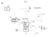
- FIG. 1 illustrates a conventional circuit for driving a solenoid valve
- FIG. 2 illustrates a circuit for driving a solenoid valve according to an embodiment of the present invention
- FIG. 3 illustrates voltages for driving the solenoid valve using the circuit of FIG. 2 ;
- FIG. 4 is a flowchart illustrating a method for driving a solenoid valve according to an embodiment of the present invention.
- the present invention relates to driving a solenoid valve at a low power.
- Embodiments of the present invention provide an apparatus for driving a solenoid at a low power that is certifiable as intrinsically safe (IS).
- IS intrinsically safe
- FIG. 1 illustrates a conventional circuit for driving a solenoid valve. It is to be understood that the functions various circuit elements, such as capacitors, diodes, etc., shown in FIG. 1 are well known to those skilled in the art and will not be described herein in detail. As illustrated in FIG. 1 , circuit 100 includes a solenoid valve 102.
- a zener diode 116 is connected in parallel with the solenoid valve 102 in order to protect the solenoid valve 102 by suppressing over-voltages applied to the solenoid valve 102.
- zener diode 116 is shown in FIG. 1 , it is to be understood that an ordinary diode of sufficient voltage and current rating can be used in place of zener diode 116.
- circuit 100 uses a 5V voltage source 104 as a primary voltage supply.
- Capacitor 118 stores voltage generated by voltage source 104.
- a voltage doubler circuit 106 doubles the 5V to generate a 10V potential, which is stored in capacitor 108.
- the voltage doubler circuit 106 can be implemented using an LTC1144, or other well known devices.
- Transistors 110 and 112 are used to selectively apply the holding voltage (5V) from voltage source 104 and the boost voltage (10V) from the voltage doubler 106 to the solenoid valve 102.
- the transistor gates of transistor 112 In order to control the solenoid valve 102 with minimum loss, the transistor gates of transistor 112 must be driven at several volts greater than the 10V that is being supplied from the voltage doubler 106 in order to minimize loss in transistor 112. Therefore, a high side mosfet driver 114, such as a monolithic integrated circuit (IC), is used to generate an even higher potential of approximately 15V when the solenoid valve 102 is actuated.
- a high side mosfet driver 114 such as a monolithic integrated circuit (IC), is used to generate an even higher potential of approximately 15V when the solenoid valve 102 is actuated.
- the mosfet driver 114 applies the 15V to transistor 112 to turn on transistor 112, thus applying the boost voltage of 10V to the solenoid valve 102.
- the diode 124 prevents current from the higher potential 10V at the source of transistor 110 back to the lower potential 5V supply 104 through the parasitic reverse diode of transistor 110. This is due to the fact that a mosfet transistor is well known to have a parasitic diode between the source and drain when the voltage is reversed from the normal polarity across the drain and source.
- the transistor would provide an undesirable current path from the 10V coil voltage to the 5V source voltage, thus rendering the boost circuit as ineffective.
- the 10V boost voltage is removed by shutting off the drive to transistor 112.
- the mosfet driver 114 turns on transistor 110 in order to apply the hold voltage of 5V to the solenoid valve 102.
- the 5V hold voltage is sufficient to supply enough energy to hold the solenoid valve 102 in a steady state "on" position.
- Capacitors 120 and 122 are supplementary to the implementation of the high side mosfet switch driver 114, as they store the boosted 15V gate drive voltage for each transistor 112 and 110, respectively.
- IS intrinsically safe
- IEC 60079-11 International Electrical Commission (IEC) IEC 60079-11, Factory Mutual (FM) 3610, Underwriters Laboratories (UL) UL913, etc.
- FM Factory Mutual
- UL Underwriters Laboratories
- IEC 60079-11 would require a designer to limit the total stored energy in an IS circuit such that, in the case of circuit 100 of FIG. 1 , all voltages associated with all capacitances must be evaluated as potential energy discharge sources that could lead to conditions for ignition while exposed to certain gaseous mixtures.
- the allowed capacitance is ten times greater for 10V than for 15V. Further, while 5V is one-half of 10V, the allowed capacitance for 5V may be interpreted to be orders of magnitude higher than the allowed capacitance for 10V. Therefore, where large amounts of capacitance are required in IS circuitry, lower voltages are highly advantageous.
- the capacitance used in the circuit of FIG. 1 is typically not a small value when evaluated for IS.
- the capacitance of capacitor 108, charged to 10 V may easily be 20 ⁇ f or greater depending on the type of solenoid and the effort required of the solenoid. Disregarding all the other capacitors and voltages, this value alone does not meet with the IS voltage-capacitance limits shown in Table 1 above.
- Another significant problem for an IS circuit is when two or more of the above cases (i.e., two or more voltages associated with capacitances) are present in the same circuit. This creates a multi-dimensional IS analysis. It is not possible, nor is it permitted, to justify such combinations by analysis under an IS standard. Instead, certifying agencies, such as Underwriters Laboratories (UL), Canadian Standards Association (CSA), or Committee for Electrotechnical Standardization (Cenelec), perform tests on these combinations using actual explosive mixtures of gases and producing sparks with faults introduced into the circuit. There is a much more significant cost and time burden associated with proving an IS design in this manner rather than by straightforward analysis based on an IS standard. This more complex testing scenario also leads to inefficient "trial and error" design/test cycles.
- UL Underwriters Laboratories
- CSA Canadian Standards Association
- Cenelec Committee for Electrotechnical Standardization
- the conventional circuit 100 shown in FIG. 1 contains three voltages of 5V, 10V, and 15V (104, 106, and 114) and capacitances (118, 108, 120 and 122) at all three voltages. This design, by definition, must take the much more difficult testing route through IS certification. Although it is to be understood that conventional circuits may not be limited to the voltages shown in FIG. 1 , any such arrangement of multiple voltages at multiple values, with various types of solenoids, will produce these same problems.
- FIG. 2 illustrates an IS circuit for driving a solenoid valve according to an embodiment of the present invention.
- the circuit 200 of FIG. 2 can be proven as IS by analysis under an IS standard, such as IEC 60079-11.
- IEC 60079-11 One premise of IS certification is that the ground circuit is always "infallible". Accordingly, the IS equipment must be installed with certain measures to guarantee the infallible ground path. Therefore, the energy sources are always referenced to the ground potential when analyzed or when tested.
- An advantageous aspect to the design of circuit 200 of FIG. 2 is that circuit 200 uses more than one driving potential to drive the solenoid valve 202, but does not use large potentials with respect to ground.
- circuit 200 includes a solenoid 202.
- a zener diode 204 is connected in parallel with the solenoid valve 202 in order to protect the solenoid valve 202 by suppressing over-voltages applied to the solenoid valve 202.
- zener diode 204 is shown in FIG. 2 , it is to be understood that other circuit components, such as an ordinary diode of sufficient voltage and current rating, can be used in place of zener diode 204.
- a voltage source 206 generates a voltage of 5V, which is stored by capacitor 220 and applied to a "high" side of the solenoid valve 202.
- the circuit 200 includes a voltage inverter 208 that is connected to voltage source 206 and generates a negative 5V potential from the 5V generated by voltage source 206.
- the voltage inverter 208 can be implemented using an integrated circuit, such as an LTC1144 or the like.
- the -5V potential generated by the voltage inverter is stored by capacitor 222. Accordingly, the elements of circuit 200 are arranged such that -5V is generated with respect to ground 224.
- controller 210 may be implemented as a microprocessor, but the present invention is not limited thereto.
- the holding potential is accomplished by transistor 212 ("hold transistor") connecting the low side of the solenoid valve 202 to ground in response to a hold control signal from the controller 210.
- the boost potential comes in the form of a negative potential (-5V) briefly applied to the low side of the solenoid valve 202 by transistor 214 ("boost transistor”) in response to a boost control signal from the controller 210.
- the controller 210 can utilize 0 to 5V digital circuits to generate the control signals. Accordingly, a hold control signal of 5V turns on the holding potential by controlling the hold transistor 212 to connect the low side of solenoid valve 202 to ground, and a hold control signal of 0V turns off the holding potential. Similarly, a boost control signal of 5V turns on the boosting potential by controlling the boosting transistor 214 to connect the -5V potential to the low side of the solenoid valve 202, and a boost control signal of 0V turns off the boost potential.
- transistors 212 and 214 of FIG. 2 are driven by simple 5V logic levels, which requires less circuitry and one less unique voltage, as opposed to the 15V gate drive potentials generated by the mosfet driver 114 in FIG. 1 .
- the hold transistor 212 and the boost transistor 214 are both turned on to apply +5V to the high side of the solenoid valve 202 and -5V to the low side of the solenoid valve 202, resulting in a 10V total boost voltage across the solenoid valve 202.
- the boost transistor is turned off so that only a 5V holding voltage is applied to the solenoid valve 202, thus reducing the power to approximately one fourth of the power used if the actuating potential were maintained at the solenoid.
- FIG. 3 illustrates voltages for driving the solenoid valve 202 of FIG. 2 .
- FIG. 3 is described while referring to the circuit 200 of FIG. 2 .
- graph 310 shows the hold control voltage applied to the hold transistor 212
- graph 320 shows the boost control voltage applied to the boost transistor 214
- graph 330 shows the voltage at the low side of the solenoid valve 202
- graph 340 shows the total voltage applied to the solenoid valve 202.
- the solenoid valve 202 is off.
- no hold control voltage 310 is being applied to the hold transistor 212 and no boost control voltage 320 is being applied to the boost transistor 214.
- the high side of the solenoid valve 202 is connected to the 5V voltage source 206, but the low side of the solenoid valve 202 is not connected to ground during t0. This results in a voltage 330 at the low side of the solenoid valve 202 of 5V, and a total voltage 340 applied to the solenoid valve of 0V, thus the solenoid is not actuated.
- the hold control voltage 310 of 5V is applied to the hold transistor 212 and the boost control voltage 320 of 5V is applied to the boost transistor 214 in order to provide a boost voltage for a time period t1 to turn on or actuate the solenoid valve 202.
- time period t1 may be much shorter than time period t2, as the boost voltage is only applied for an amount of time necessary to overcome momentum when actuating the solenoid valve.
- the hold control voltage 310 is shut off in order to turn off the solenoid valve 202, resulting in a total voltage 340 of 0V being applied to the solenoid valve 202.
- the voltages of +5V and -5V in the circuit 200 of FIG. 2 still present a 10V total boost voltage to the solenoid valve 202, and a 5V holding voltage upon release of the boost voltage.
- the fact that two voltages of opposite magnitude are present is inconsequential, given that both are referenced to the infallible ground circuit. Therefore, the absolute value of each voltage can be evaluated with respect to the IEC 60079-11 standard, as long as infallible grounding is provided to each capacitance element involved. This is especially beneficial where the magnitudes of the voltages are the same with respect to the safety ground, as shown in this example, for a magnitude of 5V.
- the circuit 200 of FIG. 2 can be analyzed under an IS standard to prove that the circuit 200 is IS. This allows circuit designers to easily ensure that such a circuit will be safe for use in a hazardous area.
- capacitors 220 and 222 are in series with a total of 10V across the series path while boosting the solenoid, whereas in circuit 100 of FIG. 1 , capacitor 108 has all of 10V of charge.
- capacitors 220 and 222 of FIG. 2 are in series with one another and the valve potential, in order to be equivalent to the capacitance of a single capacitor charged to 10V, capacitors 220 and 222 of FIG. 2 must each be two times the value of capacitors 108 or 118 of FIG. 1 .
- capacitors 220 and 222 of FIG. 2 each have a capacitance of 40 ⁇ f in order to match the level of energy required to boost the solenoid.
- Each of capacitors 220 and 222 having a capacitance of 40 ⁇ f results in a total of 80 ⁇ f at a magnitude of 5V (assuming +5V and -5V circuits, both referenced to ground a paralleled and evaluated as one lump sum capacitance at a magnitude of 5V). This may seem detrimental until referring to Table 1 above (or referring to an IS standard such as IEC 60079-11), which shows that decreases in voltage allow for large increases in capacitance which do not follow a linear relationship, but rather allow for multiples of additional capacitance when the voltage is simply cut in half from 10V to 5V.
- the amount of capacitance needed for capacitors 220 and 222 in the above described example is well within the permissible capacitance at 5V, and there is no doubt that these requirements are met. Furthermore, this allows the circuit 200 to be proven as IS by analysis using just one low voltage magnitude and fitting within proven methods for establishing safe conditions, thus saving tremendous certification costs while ensuring that the circuit 200 is safe for use in a hazardous area.
- the circuit 200 of FIG. 2 is an IS circuit for driving a solenoid valve. It is to be understood that in order to be IS, additional IS requirements must be followed in the design of the circuit according to a particular IS standard. For example certain circuit elements, such as the 5V voltage source 206 and the -5V voltage source (voltage inverter) 208, may be required to be physically spaced apart by a certain amount. Table 5 of the IEC 60079-11 standard establishes criteria for the minimum conductor clearance and creepage spacing between separate voltages, so as to not allow a fault connection between these voltages. In addition, it is to be understood that the circuit 200 of FIG. 2 is an IS circuit that may be implemented as part of a larger IS device or system. Furthermore, although the embodiment described in FIG. 2 uses certain values for voltages and capacitances, the present invention is not limited to these values.
- FIG. 4 is a flowchart illustrating a method of driving a solenoid valve according to an embodiment of the present invention.
- the method of FIG. 4 may be performed by a circuit, such as circuit 200 of FIG. 2 .
- a solenoid valve is actuated by applying a first voltage to a first side of the solenoid valve and a second voltage to a second side of the solenoid valve.
- the second voltage is a voltage of opposite magnitude to the first voltage, so that the total voltage across the solenoid valve is twice the first voltage.
- the first voltage can be applied to a high side of the solenoid valve and the second voltage can be applied to a low side of the solenoid valve.
- the first and second voltages can be applied to the solenoid valve in response to first and second control signals from a controller.
- the hold control signal and the boost control signal from controller 210 respectively activate the hold transistor 212 and the boost transistor 214 to apply 5V to the high side of solenoid valve 202 and -5V to the low side of solenoid valve 202, for a total of 10V applied to solenoid valve 202.
- the solenoid valve is held in an on position by controlling the second voltage not to be applied to the second side of the solenoid valve while controlling the first voltage to continue to be applied to the first side of the solenoid valve. Accordingly, once the solenoid valve has been actuated and has overcome momentum, the voltage is reduced by removing the second voltage and maintaining the low side of the solenoid at ground potential. The second voltage can be controlled to no longer be applied to the solenoid valve in response to the release of the second control signal from the controller. When the second voltage is removed, the low side of the solenoid is instead applied to ground potential while the solenoid is on. For example, in circuit 200 of FIG.
- the controller 210 shuts off the boost control signal in order to control the boost transistor 214 to disconnect the voltage inverter 208 (generating -5V) from the low side of the solenoid valve 202.
- the controller 210 maintains the hold control signal so that 5V is still applied to the solenoid valve 202 to keep the solenoid valve running at steady state.
- the solenoid valve is shut off by controlling the first voltage not to be applied to the solenoid valve.
- the first voltage is controlled to no longer be applied to the solenoid valve in response to the release of the first control signal from the controller.
- the controller 210 shuts off the hold control signal in order to control the hold transistor 212 to disconnect the low side of the solenoid valve 202 from the ground in order to stop the 5V from voltage source 206 from being applied across the solenoid valve 202.
- Embodiments of the present invention described above provide a circuit that utilizes a reduced voltage, which allows the use of capacitance high enough to effectively overcome inertia and actuate a solenoid valve while still being compliant with IS standards. Also, embodiments of the present invention described above provide a circuit allows for higher power solenoids to comply with IS standards Further, embodiments of the present invention described above provide a circuit that is certifiable as IS without complex and expensive testing procedures.
Abstract
Description
- This application claims the benefit of
U.S. Provisional Application No. 61/046,001, filed April 18, 2008 U.S. Provisional Application No. 61,046,076, filed April 18, 2008 U.S. Provisional Application No. 61,104,767, filed April 25, 2008 - The present invention relates to driving a solenoid valve at a low power, and more particularly to an apparatus and method for driving a solenoid valve at low power that is certifiable as intrinsically safe.
- A solenoid valve is an electromechanical device commonly used to control the flow of gas or liquid by running an electric current through a solenoid, which is a magnetic coil. It is well known that a solenoid, or any electromechanical device with a magnetic coil, may be actuated at a higher voltage (power) and the voltage can be reduced to a lower voltage to "hold" the solenoid in the "on" position. The higher voltage overcomes inertia to start the movement of the solenoid, and the reduction to the lower voltage reduces power consumption in driving the solenoid.
- Reducing power consumption is very desirable, particularly for circuits used to drive a solenoid valve in a process instrument sample system. However, the challenge that arises for process instrumentation is that such a circuit to drive a solenoid must use a protection technique that is suitable for the hazardous area in which it is present. Due to the difficulty of wiring to explosion-proof mechanically protected equipment, Intrinsically Safe (IS) circuits are desirable. Intrinsic safety is a protection concept deployed in sensitive or potentially explosive atmospheres. Intrinsic safety relies on equipment designed so that it is unable to release sufficient energy, by either thermal or electrical means, to contribute to conditions that are favorable for ignition of a flammable gas. There are various IS standards set forth by various certifying agencies for a system to be considered IS. Such standards include International Electrical Commission (IEC) IEC 60079-11, Factory Mutual (FM) 3610, Underwriters Laboratories (UL) UL913, etc.
- Conventional circuit designs for driving a solenoid typically utilize multiple voltages, which makes such circuits difficult to certify as IS by analysis based on an IS standard. In such cases, certifying agencies must perform tests on the circuit designs using actual explosive mixtures of gases, and producing sparks with faults introduced into the circuit. Such testing is much more costly and time consuming than proving an IS design by straightforward analysis. Further, such testing leads to inefficient "trial and error" design/test cycles because it is difficult for a designer to anticipate whether the circuit design will be accepted to be IS by the certifying agency. This testing approach also makes it much more difficult to modify or iterate the design without re-test. Also, for some solenoid valves, if the inertial energy requirements to actuate the solenoid valves are high, it may not be possible for conventional circuit designs to comply to IS standards.
- The present invention relates to driving a solenoid valve at a low power using an apparatus that is certifiable as intrinsically safe (IS). Embodiments of the present invention provide a circuit that utilizes a reduced voltage, which allows the use of capacitance and voltage across a solenoid that is high enough to deliver enough energy to effectively overcome the effects of inertia and actuate a solenoid valve, while still being compliant with IS standards. Further, embodiments of the present invention provide a circuit that is certifiable as IS without complex and expensive testing procedures.
- In one embodiment of the present invention, a voltage source generates a first voltage and is connected to a first side of a solenoid valve. A voltage inverter is connected to the voltage source and generates a second voltage from the first voltage. The second voltage is of opposite magnitude to the first voltage. A controller selectively controls the first voltage and the second voltage to be applied to the solenoid valve. In order to actuate the solenoid valve, the first voltage is applied to the first side of the solenoid valve and the second voltage is applied to the second side of the solenoid valve. In order to hold the solenoid valve in an on position, the first voltage is maintained and the second voltage is no longer applied to the second side of the solenoid valve, with the second side of the solenoid instead directed to ground potential with respect to the first voltage.
- These and other advantages of the invention will be apparent to those of ordinary skill in the art by reference to the following detailed description and the accompanying drawings.
-
FIG. 1 illustrates a conventional circuit for driving a solenoid valve; -
FIG. 2 illustrates a circuit for driving a solenoid valve according to an embodiment of the present invention; -
FIG. 3 illustrates voltages for driving the solenoid valve using the circuit ofFIG. 2 ; and -
FIG. 4 is a flowchart illustrating a method for driving a solenoid valve according to an embodiment of the present invention. - The present invention relates to driving a solenoid valve at a low power. Embodiments of the present invention provide an apparatus for driving a solenoid at a low power that is certifiable as intrinsically safe (IS).
- It is well known that a solenoid, or any electromechanical device with a magnetic coil, may be actuated at a higher power and then held in place in a static on position with a lower power after the inertia of movement has been overcome.
FIG. 1 illustrates a conventional circuit for driving a solenoid valve. It is to be understood that the functions various circuit elements, such as capacitors, diodes, etc., shown inFIG. 1 are well known to those skilled in the art and will not be described herein in detail. As illustrated inFIG. 1 ,circuit 100 includes asolenoid valve 102. Azener diode 116 is connected in parallel with thesolenoid valve 102 in order to protect thesolenoid valve 102 by suppressing over-voltages applied to thesolenoid valve 102. Althoughzener diode 116 is shown inFIG. 1 , it is to be understood that an ordinary diode of sufficient voltage and current rating can be used in place ofzener diode 116. In this example,circuit 100 uses a5V voltage source 104 as a primary voltage supply.Capacitor 118 stores voltage generated byvoltage source 104. Avoltage doubler circuit 106 doubles the 5V to generate a 10V potential, which is stored incapacitor 108. For example, thevoltage doubler circuit 106 can be implemented using an LTC1144, or other well known devices.Transistors voltage source 104 and the boost voltage (10V) from thevoltage doubler 106 to thesolenoid valve 102. In order to control thesolenoid valve 102 with minimum loss, the transistor gates oftransistor 112 must be driven at several volts greater than the 10V that is being supplied from thevoltage doubler 106 in order to minimize loss intransistor 112. Therefore, a highside mosfet driver 114, such as a monolithic integrated circuit (IC), is used to generate an even higher potential of approximately 15V when thesolenoid valve 102 is actuated. - In order to actuate the
solenoid valve 102, in response to a boost control signal, themosfet driver 114 applies the 15V totransistor 112 to turn ontransistor 112, thus applying the boost voltage of 10V to thesolenoid valve 102. During this time, there is a 10V potential at the source oftransistor 110. Thediode 124 prevents current from thehigher potential 10V at the source oftransistor 110 back to thelower 104 through the parasitic reverse diode ofpotential 5V supplytransistor 110. This is due to the fact that a mosfet transistor is well known to have a parasitic diode between the source and drain when the voltage is reversed from the normal polarity across the drain and source. Without the blocking action ofdiode 124, the transistor would provide an undesirable current path from the 10V coil voltage to the 5V source voltage, thus rendering the boost circuit as ineffective. A short time after the boost voltage of 10V is applied, once the solenoid has overcome inertia, the 10V boost voltage is removed by shutting off the drive totransistor 112. At the same time astransistor 112 is turned on, or any time beforetransistor 112 is shut off, in response to a hold voltage signal, themosfet driver 114 turns ontransistor 110 in order to apply the hold voltage of 5V to thesolenoid valve 102. The 5V hold voltage is sufficient to supply enough energy to hold thesolenoid valve 102 in a steady state "on" position. Accordingly, by removing the 10V boost voltage and using the 5V hold voltage to keep thesolenoid valve 102 in the on position, the steady state power requirements ofcircuit 100 are reduced.Capacitors mosfet switch driver 114, as they store the boosted 15V gate drive voltage for eachtransistor - The reduction of voltage in driving the solenoid valve poses a significant power advantage because half of the voltage may correlate to a quarter of the power. In the case of process instrument sample system control, the cost benefit can typically be $300-$400 per watt of power capacity for an installed system. Accordingly, driving a solenoid with the lowest possible power is desirable.
- The challenge that arises for designers of process instrumentation is that such devices are often required to be intrinsically safe (IS) due to their presence in a hazardous area. As described above, there are various IS standards set forth by various certifying agencies for a system to be considered IS. Such standards include International Electrical Commission (IEC) IEC 60079-11, Factory Mutual (FM) 3610, Underwriters Laboratories (UL) UL913, etc. The most commonly cited safety standard, IEC 60079-11, would require a designer to limit the total stored energy in an IS circuit such that, in the case of
circuit 100 ofFIG. 1 , all voltages associated with all capacitances must be evaluated as potential energy discharge sources that could lead to conditions for ignition while exposed to certain gaseous mixtures. In making a circuit IS, a designer seeks to eliminate any such potential of ignition. As long as only one voltage is involved, it is possible to determine by established curves and tables in IEC 60079-11 whether the capacitance and voltage values are low enough to ensure that the circuit is "safe". Since a capacitor is considered an energy storage device, the voltage has a significant factor on the amount of capacitance that is allowed in an IS circuit. For example, Table 1 below shows approximate capacitance limits for different voltage levels based on an interpretation of curves in the IEC 60079-11 standard.Table 1 IEC60079-11 Figure A.3 Group II Capacitance Curve Data Voltage Capacitance (approximate limit) 15 volts <1 micro-farad 10 volts <10 micro-farad 5 volts asymptotic curve to 1000 uf or more - As illustrated in Table 1, while the ratio between 15V and 10V is 1.5, the allowed capacitance is ten times greater for 10V than for 15V. Further, while 5V is one-half of 10V, the allowed capacitance for 5V may be interpreted to be orders of magnitude higher than the allowed capacitance for 10V. Therefore, where large amounts of capacitance are required in IS circuitry, lower voltages are highly advantageous.
- The capacitance used in the circuit of
FIG. 1 is typically not a small value when evaluated for IS. In order to store enough energy to provide an adequate boost voltage for the required time, the capacitance ofcapacitor 108, charged to 10 V, may easily be 20 µf or greater depending on the type of solenoid and the effort required of the solenoid. Disregarding all the other capacitors and voltages, this value alone does not meet with the IS voltage-capacitance limits shown in Table 1 above. - Another significant problem for an IS circuit is when two or more of the above cases (i.e., two or more voltages associated with capacitances) are present in the same circuit. This creates a multi-dimensional IS analysis. It is not possible, nor is it permitted, to justify such combinations by analysis under an IS standard. Instead, certifying agencies, such as Underwriters Laboratories (UL), Canadian Standards Association (CSA), or Committee for Electrotechnical Standardization (Cenelec), perform tests on these combinations using actual explosive mixtures of gases and producing sparks with faults introduced into the circuit. There is a much more significant cost and time burden associated with proving an IS design in this manner rather than by straightforward analysis based on an IS standard. This more complex testing scenario also leads to inefficient "trial and error" design/test cycles.
- The
conventional circuit 100 shown inFIG. 1 contains three voltages of 5V, 10V, and 15V (104, 106, and 114) and capacitances (118, 108, 120 and 122) at all three voltages. This design, by definition, must take the much more difficult testing route through IS certification. Although it is to be understood that conventional circuits may not be limited to the voltages shown inFIG. 1 , any such arrangement of multiple voltages at multiple values, with various types of solenoids, will produce these same problems. - Embodiments of the present invention overcome the above described problems with intrinsic safety in conventional circuits for driving a solenoid valve.
FIG. 2 illustrates an IS circuit for driving a solenoid valve according to an embodiment of the present invention. Thecircuit 200 ofFIG. 2 can be proven as IS by analysis under an IS standard, such as IEC 60079-11. One premise of IS certification is that the ground circuit is always "infallible". Accordingly, the IS equipment must be installed with certain measures to guarantee the infallible ground path. Therefore, the energy sources are always referenced to the ground potential when analyzed or when tested. An advantageous aspect to the design ofcircuit 200 ofFIG. 2 is thatcircuit 200 uses more than one driving potential to drive thesolenoid valve 202, but does not use large potentials with respect to ground. - As illustrated in
FIG. 2 ,circuit 200 includes asolenoid 202. Azener diode 204 is connected in parallel with thesolenoid valve 202 in order to protect thesolenoid valve 202 by suppressing over-voltages applied to thesolenoid valve 202. Althoughzener diode 204 is shown inFIG. 2 , it is to be understood that other circuit components, such as an ordinary diode of sufficient voltage and current rating, can be used in place ofzener diode 204. Avoltage source 206 generates a voltage of 5V, which is stored bycapacitor 220 and applied to a "high" side of thesolenoid valve 202. Thecircuit 200 includes avoltage inverter 208 that is connected tovoltage source 206 and generates a negative 5V potential from the 5V generated byvoltage source 206. For example, thevoltage inverter 208 can be implemented using an integrated circuit, such as an LTC1144 or the like. The -5V potential generated by the voltage inverter is stored bycapacitor 222. Accordingly, the elements ofcircuit 200 are arranged such that -5V is generated with respect toground 224. - In
circuit 200, the "high" side of thesolenoid valve 202 always sees 5V, however, the "low" side is controlled with boost and holding potentials based on boost and hold control signals fromcontroller 210. According to an advantageous implementation,controller 210 may be implemented as a microprocessor, but the present invention is not limited thereto. The holding potential is accomplished by transistor 212 ("hold transistor") connecting the low side of thesolenoid valve 202 to ground in response to a hold control signal from thecontroller 210. The boost potential comes in the form of a negative potential (-5V) briefly applied to the low side of thesolenoid valve 202 by transistor 214 ("boost transistor") in response to a boost control signal from thecontroller 210. Thecontroller 210 can utilize 0 to 5V digital circuits to generate the control signals. Accordingly, a hold control signal of 5V turns on the holding potential by controlling thehold transistor 212 to connect the low side ofsolenoid valve 202 to ground, and a hold control signal of 0V turns off the holding potential. Similarly, a boost control signal of 5V turns on the boosting potential by controlling the boostingtransistor 214 to connect the -5V potential to the low side of thesolenoid valve 202, and a boost control signal of 0V turns off the boost potential. Since 0 to 5V digital circuits are used as the control circuits, the arrangement ofzener diode 216,resistor 218 and pull downtransistor 214 form a simple level translation that does not interfere with the 5V digital interface and does not require additional cumbersome gate drive potentials. It can be noted that unlike incircuit 100 ofFIG. 1 , where a separate high side transistor drive voltage was required,transistors FIG. 2 are driven by simple 5V logic levels, which requires less circuitry and one less unique voltage, as opposed to the 15V gate drive potentials generated by themosfet driver 114 inFIG. 1 . - In order to actuate the
solenoid valve 202, thehold transistor 212 and theboost transistor 214 are both turned on to apply +5V to the high side of thesolenoid valve 202 and -5V to the low side of thesolenoid valve 202, resulting in a 10V total boost voltage across thesolenoid valve 202. Once thesolenoid valve 202 has overcome the inertia of movement, the boost transistor is turned off so that only a 5V holding voltage is applied to thesolenoid valve 202, thus reducing the power to approximately one fourth of the power used if the actuating potential were maintained at the solenoid. -
FIG. 3 illustrates voltages for driving thesolenoid valve 202 ofFIG. 2 .FIG. 3 is described while referring to thecircuit 200 ofFIG. 2 . As illustrated inFIG. 3 ,graph 310 shows the hold control voltage applied to thehold transistor 212,graph 320 shows the boost control voltage applied to theboost transistor 214,graph 330 shows the voltage at the low side of thesolenoid valve 202, andgraph 340 shows the total voltage applied to thesolenoid valve 202. For the time period t0, thesolenoid valve 202 is off. During this time period t0, nohold control voltage 310 is being applied to thehold transistor 212 and noboost control voltage 320 is being applied to theboost transistor 214. The high side of thesolenoid valve 202 is connected to the5V voltage source 206, but the low side of thesolenoid valve 202 is not connected to ground during t0. This results in avoltage 330 at the low side of thesolenoid valve 202 of 5V, and atotal voltage 340 applied to the solenoid valve of 0V, thus the solenoid is not actuated. At 302, thehold control voltage 310 of 5V is applied to thehold transistor 212 and theboost control voltage 320 of 5V is applied to theboost transistor 214 in order to provide a boost voltage for a time period t1 to turn on or actuate thesolenoid valve 202. This results in avoltage 330 of -5V at the low side of the solenoid valve, and atotal voltage 340 of 10V applied to thesolenoid valve 202 for the time period t1. At 304, thehold control voltage 310 is maintained at 5V and theboost control voltage 320 is turned off (0V) in order to hold thesolenoid valve 202 turned on at steady state for time period t2. This results in avoltage 330 of 0V at the low side of thesolenoid valve 202, and atotal voltage 340 of 5V being applied to the solenoid valve, which holds the solenoid valve in an on position for time period t2. It can be noted that time period t1 may be much shorter than time period t2, as the boost voltage is only applied for an amount of time necessary to overcome momentum when actuating the solenoid valve. At 306, thehold control voltage 310 is shut off in order to turn off thesolenoid valve 202, resulting in atotal voltage 340 of 0V being applied to thesolenoid valve 202. - As described above, the voltages of +5V and -5V in the
circuit 200 ofFIG. 2 still present a 10V total boost voltage to thesolenoid valve 202, and a 5V holding voltage upon release of the boost voltage. For IS analysis, the fact that two voltages of opposite magnitude are present is inconsequential, given that both are referenced to the infallible ground circuit. Therefore, the absolute value of each voltage can be evaluated with respect to the IEC 60079-11 standard, as long as infallible grounding is provided to each capacitance element involved. This is especially beneficial where the magnitudes of the voltages are the same with respect to the safety ground, as shown in this example, for a magnitude of 5V. Accordingly, thecircuit 200 ofFIG. 2 can be analyzed under an IS standard to prove that thecircuit 200 is IS. This allows circuit designers to easily ensure that such a circuit will be safe for use in a hazardous area. - Regarding capacitance in the
circuit 200, there is a tradeoff that is needed, but it is an advantageous tradeoff. If in thecircuit 100 ofFIG. 1 , 20 µf of capacitance at 10V is required for the boost voltage, then this can be related to a level of energy that is required to boost the solenoid. The potential drawback of having a +5V and -5V voltage supply (incircuit 200 ofFIG. 2 ), instead of a total 10V supply (incircuit 100 ofFIG. 1 ), is that from an AC or transient perspective,capacitors circuit 100 ofFIG. 1 ,capacitor 108 has all of 10V of charge. The net effect is that sincecapacitors FIG. 2 are in series with one another and the valve potential, in order to be equivalent to the capacitance of a single capacitor charged to 10V,capacitors FIG. 2 must each be two times the value ofcapacitors FIG. 1 . Using above described example in which capacitor 108 ofFIG. 1 has a capacitance of 20 µf, this meanscapacitors FIG. 2 each have a capacitance of 40 µf in order to match the level of energy required to boost the solenoid. Each ofcapacitors capacitors circuit 200 to be proven as IS by analysis using just one low voltage magnitude and fitting within proven methods for establishing safe conditions, thus saving tremendous certification costs while ensuring that thecircuit 200 is safe for use in a hazardous area. - The
circuit 200 ofFIG. 2 is an IS circuit for driving a solenoid valve. It is to be understood that in order to be IS, additional IS requirements must be followed in the design of the circuit according to a particular IS standard. For example certain circuit elements, such as the5V voltage source 206 and the -5V voltage source (voltage inverter) 208, may be required to be physically spaced apart by a certain amount. Table 5 of the IEC 60079-11 standard establishes criteria for the minimum conductor clearance and creepage spacing between separate voltages, so as to not allow a fault connection between these voltages. In addition, it is to be understood that thecircuit 200 ofFIG. 2 is an IS circuit that may be implemented as part of a larger IS device or system. Furthermore, although the embodiment described inFIG. 2 uses certain values for voltages and capacitances, the present invention is not limited to these values. -
FIG. 4 is a flowchart illustrating a method of driving a solenoid valve according to an embodiment of the present invention. The method ofFIG. 4 may be performed by a circuit, such ascircuit 200 ofFIG. 2 . Atstep 402, a solenoid valve is actuated by applying a first voltage to a first side of the solenoid valve and a second voltage to a second side of the solenoid valve. The second voltage is a voltage of opposite magnitude to the first voltage, so that the total voltage across the solenoid valve is twice the first voltage. The first voltage can be applied to a high side of the solenoid valve and the second voltage can be applied to a low side of the solenoid valve. The first and second voltages can be applied to the solenoid valve in response to first and second control signals from a controller. For example, incircuit 200 ofFIG. 2 , the hold control signal and the boost control signal fromcontroller 210 respectively activate thehold transistor 212 and theboost transistor 214 to apply 5V to the high side ofsolenoid valve 202 and -5V to the low side ofsolenoid valve 202, for a total of 10V applied tosolenoid valve 202. - At
step 404, the solenoid valve is held in an on position by controlling the second voltage not to be applied to the second side of the solenoid valve while controlling the first voltage to continue to be applied to the first side of the solenoid valve. Accordingly, once the solenoid valve has been actuated and has overcome momentum, the voltage is reduced by removing the second voltage and maintaining the low side of the solenoid at ground potential. The second voltage can be controlled to no longer be applied to the solenoid valve in response to the release of the second control signal from the controller. When the second voltage is removed, the low side of the solenoid is instead applied to ground potential while the solenoid is on. For example, incircuit 200 ofFIG. 2 , thecontroller 210 shuts off the boost control signal in order to control theboost transistor 214 to disconnect the voltage inverter 208 (generating -5V) from the low side of thesolenoid valve 202. Thecontroller 210 maintains the hold control signal so that 5V is still applied to thesolenoid valve 202 to keep the solenoid valve running at steady state. - At
step 406, the solenoid valve is shut off by controlling the first voltage not to be applied to the solenoid valve. At this point, neither the first voltage nor the second voltage is applied to the solenoid valve. The first voltage is controlled to no longer be applied to the solenoid valve in response to the release of the first control signal from the controller. For example, incircuit 200 ofFIG. 2 , thecontroller 210 shuts off the hold control signal in order to control thehold transistor 212 to disconnect the low side of thesolenoid valve 202 from the ground in order to stop the 5V fromvoltage source 206 from being applied across thesolenoid valve 202. - As described above, the extra energy needed to for a conventional circuit to drive a solenoid makes it difficult for such a conventional circuit to be IS. In addition, conventional circuits used to drive a solenoid at a reduced power require complex testing to be certified as IS. Embodiments of the present invention described above provide a circuit that utilizes a reduced voltage, which allows the use of capacitance high enough to effectively overcome inertia and actuate a solenoid valve while still being compliant with IS standards. Also, embodiments of the present invention described above provide a circuit allows for higher power solenoids to comply with IS standards Further, embodiments of the present invention described above provide a circuit that is certifiable as IS without complex and expensive testing procedures.
- The foregoing Detailed Description is to be understood as being in every respect illustrative and exemplary, but not restrictive, and the scope of the invention disclosed herein is not to be determined from the Detailed Description, but rather from the claims as interpreted according to the full breadth permitted by the patent laws. It is to be understood that the embodiments shown and described herein are only illustrative of the principles of the present invention and that various modifications may be implemented by those skilled in the art without departing from the scope and spirit of the invention. Those skilled in the art could implement various other feature combinations without departing from the scope and spirit of the invention.
Claims (24)
- An apparatus for driving a solenoid valve comprising:a solenoid valve;a voltage source connected to a first side of the solenoid valve and configured to generate a first voltage;a voltage inverter connected to the voltage source and configured to generate a second voltage from the first voltage, wherein the second voltage is of opposite magnitude to the first voltage; anda controller configured to selectively control the first voltage and the second voltage to be applied to the solenoid valve.
- The apparatus of claim 1, further comprising:a first transistor configured to connect a second side of the solenoid valve to a ground in response to a first control signal from the controller to apply the first voltage to the solenoid valve; anda second transistor configured to connect the second side of the solenoid valve to the voltage inverter in response to a second control signal from the controller to apply the second voltage to the solenoid valve.
- The apparatus of claim 2, wherein the first side of the solenoid valve is a high side of the solenoid valve and the second of the solenoid valve is a low side of the solenoid valve.
- The apparatus of claim 1, wherein the controller is configured to control the first voltage to be applied to the first side of the solenoid valve and the second voltage to be applied to a second side of the solenoid valve to actuate the solenoid valve.
- The apparatus of claim 4, wherein the controller is configured to control the first voltage to continue to be applied to the solenoid valve and to control the second voltage not to be applied to the solenoid valve after the solenoid valve has been actuated to hold the solenoid valve in an on position.
- The method of claim 4, wherein a total voltage applied to the solenoid valve when the first and second voltages are applied to the first and second sides of the solenoid valve, respectively, is a multiple of the first voltage.
- The apparatus of claim 1, further comprising:a first capacitor connected between the voltage source and the first side of the solenoid valve; anda second capacitor connected between the voltage inverter and a second side of the solenoid valve.
- The apparatus of claim 7, wherein a capacitance of the first and second capacitors is less than a capacitance limit corresponding to the first voltage according to an intrinsic safety standard.
- The apparatus of claim 8, wherein said intrinsic safety standard is IEC 60079-11.
- The apparatus of claim 1, wherein said apparatus is intrinsically safe (IS) according to an intrinsic safety standard.
- The apparatus of claim 1, wherein said controller comprises a microprocessor.
- A method for driving a solenoid valve, comprising:actuating the solenoid valve by controlling a first voltage to be applied to a first side of the solenoid valve and controlling a second voltage to be applied to a second side of the solenoid valve, wherein the second voltage is of opposite magnitude to the first voltage; andholding the solenoid valve in an on position by controlling the first voltage to continue to be applied to the solenoid valve and controlling the second voltage to not be applied to the second side of the solenoid valve.
- The method of claim 12, wherein the first voltage is generated by a voltage source and the second voltage is generated from the first voltage from a voltage inverter connected to the voltage source.
- The method of claim 12, said step of actuating the solenoid valve by controlling a first voltage to be applied to a first side of the solenoid valve and controlling a second voltage to be applied to a second side of the solenoid valve comprises:controlling a first transistor to connect the second side of the solenoid valve to a ground to apply the first voltage to the first side of the solenoid valve; andcontrolling a second transistor to connect the second voltage to the second side of the solenoid valve.
- The method of claim 14, wherein said step of controlling the second voltage to not be applied to the second side of the solenoid valve comprises:controlling the second transistor to disconnect the second voltage from the second side of the solenoid valve.
- The method of claim 15, further comprising:turning off the solenoid valve by controlling the first transistor to disconnect the second side of the solenoid valve from the ground.
- The method of claim 16, wherein the first and second transistors are controlled by transmitting control voltages to the first and second transistors.
- The method of claim 14, wherein the first side of the solenoid valve is a high side of the solenoid valve and the second of the solenoid valve is a low side of the solenoid valve.
- An apparatus for driving a solenoid valve comprising:means for actuating the solenoid valve by controlling a first voltage to be applied to a first side of the solenoid valve and controlling a second voltage to be applied to a second side of the solenoid valve, wherein the second voltage is of opposite magnitude to the first voltage; andmeans for holding the solenoid valve in an on position by controlling the first voltage to continue to be applied to the solenoid valve and controlling the second voltage to not be applied to the second side of the solenoid valve.
- The apparatus of claim 19, further comprising:means for generating the first voltage; andmeans for generating the second voltage by inverting the first voltage.
- The apparatus of claim 19, said means for actuating the solenoid valve by controlling a first voltage to be applied to a first side of the solenoid valve and controlling a second voltage to be applied to a second side of the solenoid valve comprises:means for controlling a first transistor to connect the second side of the solenoid valve to a ground to apply the first voltage to the first side of the solenoid valve; andmeans for controlling a second transistor to connect the second voltage to the second side of the solenoid valve.
- The apparatus of claim 21, wherein said means for holding the solenoid valve in an on position by controlling the first voltage to continue to be applied to the solenoid valve and controlling the second voltage to not be applied to the second side of the solenoid valve comprises:means for controlling the second transistor to disconnect the second voltage from the second side of the solenoid valve.
- The apparatus of claim 22, further comprising:means for turning off the solenoid valve by controlling the first transistor to disconnect the second side of the solenoid valve from the ground.
- The apparatus of claim 21, wherein the first side of the solenoid valve is a high side of the solenoid valve and the second of the solenoid valve is a low side of the solenoid valve.
Applications Claiming Priority (4)
| Application Number | Priority Date | Filing Date | Title |
|---|---|---|---|
| US4600108P | 2008-04-18 | 2008-04-18 | |
| US4607608P | 2008-04-18 | 2008-04-18 | |
| US4776708P | 2008-04-25 | 2008-04-25 | |
| US12/423,087 US8059382B2 (en) | 2008-04-18 | 2009-04-14 | Intrinsically safe circuit for driving a solenoid valve at low power |
Publications (3)
| Publication Number | Publication Date |
|---|---|
| EP2110820A2 true EP2110820A2 (en) | 2009-10-21 |
| EP2110820A3 EP2110820A3 (en) | 2014-10-22 |
| EP2110820B1 EP2110820B1 (en) | 2018-05-30 |
Family
ID=40756360
Family Applications (1)
| Application Number | Title | Priority Date | Filing Date |
|---|---|---|---|
| EP09158057.1A Not-in-force EP2110820B1 (en) | 2008-04-18 | 2009-04-16 | Intrinsically safe circuit for driving a solenoid valve at a low power |
Country Status (2)
| Country | Link |
|---|---|
| US (1) | US8059382B2 (en) |
| EP (1) | EP2110820B1 (en) |
Cited By (6)
| Publication number | Priority date | Publication date | Assignee | Title |
|---|---|---|---|---|
| EP2312188A1 (en) | 2009-10-16 | 2011-04-20 | Diener Precision Pumps Ltd. | Electronic adapter for controlling a bistable valve |
| WO2013019396A1 (en) * | 2011-08-01 | 2013-02-07 | Automatic Switch Company | System and method of assuring drop out of a solenoid valve |
| CN104747777A (en) * | 2015-03-10 | 2015-07-01 | 浙江汉特姆阀门有限公司 | Fuel gas electromagnetic valve control circuit |
| AT14641U1 (en) * | 2014-04-28 | 2016-03-15 | Valmet Technologies Inc | DIGITAL HYDRAULIC PRESSURE REGULATOR AND METHOD OF MANUFACTURING A DIGITAL HYDRAULIC PRESSURE REGULATOR |
| EP3340259A1 (en) * | 2016-12-21 | 2018-06-27 | Conti Temic microelectronic GmbH | Solenoid device |
| CN112682561A (en) * | 2021-01-11 | 2021-04-20 | 福州大学 | Drive control system and control method of high-speed switch electromagnetic valve |
Families Citing this family (9)
| Publication number | Priority date | Publication date | Assignee | Title |
|---|---|---|---|---|
| EP2584570A1 (en) * | 2011-10-21 | 2013-04-24 | Metso Paper Inc. | Booster for a digital hydraulic controller and method for using a booster in connection with a digital hydraulic controller |
| US9068440B1 (en) * | 2012-06-01 | 2015-06-30 | William Lauf | Explosion-proof magnetic flux leakage inspection apparatus for well tubing |
| CN103856205B (en) * | 2012-12-05 | 2016-04-20 | 艾尔瓦特集成电路科技(天津)有限公司 | Level shifting circuit, for driving the drive circuit of high tension apparatus and corresponding method |
| CN103291243B (en) * | 2013-05-11 | 2015-12-23 | 广东普洛测控科技有限公司 | A kind of downhole electromagnetic valve twin-stage drive circuit |
| WO2015168351A1 (en) | 2014-05-02 | 2015-11-05 | Swagelok Company | Fluid sample system and method |
| CN107580663B (en) | 2015-03-18 | 2019-04-23 | 自动开关公司 | Ensure the release of the solenoid valve by peak holding driver control |
| WO2019028345A1 (en) | 2017-08-03 | 2019-02-07 | Capstan Ag Systems, Inc. | System and methods for operating a solenoid valve |
| US10953423B2 (en) | 2018-04-23 | 2021-03-23 | Capstan Ag Systems, Inc. | Fluid dispensing apparatus including phased valves and methods of dispensing fluid using same |
| AU2021283944A1 (en) * | 2020-06-03 | 2022-12-01 | Capstan Ag Systems, Inc. | System and methods for operating a solenoid valve |
Citations (3)
| Publication number | Priority date | Publication date | Assignee | Title |
|---|---|---|---|---|
| EP0727566A2 (en) * | 1995-02-15 | 1996-08-21 | Toyota Jidosha Kabushiki Kaisha | A valve driving apparatus using an electromagnetic coil to move a valve body with reduced noise |
| EP1324477A2 (en) * | 2001-12-21 | 2003-07-02 | Fujitsu Limited | Bipolar supply voltage generator and semiconductor device for same |
| US20080083895A1 (en) * | 2006-09-20 | 2008-04-10 | Denso Corporation | Apparatus for driving electromagnetic values |
Family Cites Families (8)
| Publication number | Priority date | Publication date | Assignee | Title |
|---|---|---|---|---|
| CA2123659C (en) | 1993-05-18 | 1996-12-24 | Scott W. Braun | Solenoid control circuitry |
| US5583764A (en) * | 1994-10-18 | 1996-12-10 | M-I Drilling Fluids L.L.C. | Intrinsically safe data acquisition system and apparatus |
| US5621603A (en) | 1995-07-26 | 1997-04-15 | United Technologies Corporation | Pulse width modulated solenoid driver controller |
| US5703748A (en) | 1996-05-10 | 1997-12-30 | General Motors Corporation | Solenoid driver circuit and method |
| US5748431A (en) | 1996-10-16 | 1998-05-05 | Deere & Company | Solenoid driver circuit |
| US6256185B1 (en) | 1999-07-30 | 2001-07-03 | Trombetta, Llc | Low voltage direct control universal pulse width modulation module |
| KR100849355B1 (en) * | 2001-01-17 | 2008-07-29 | 엔엑스피 비 브이 | A controlled multi-output dc/dc converter |
| US7898786B2 (en) * | 2007-01-26 | 2011-03-01 | Siemens Industry, Inc. | Intrinsically safe galvanically isolated barrier device and method thereof |
-
2009
- 2009-04-14 US US12/423,087 patent/US8059382B2/en not_active Expired - Fee Related
- 2009-04-16 EP EP09158057.1A patent/EP2110820B1/en not_active Not-in-force
Patent Citations (3)
| Publication number | Priority date | Publication date | Assignee | Title |
|---|---|---|---|---|
| EP0727566A2 (en) * | 1995-02-15 | 1996-08-21 | Toyota Jidosha Kabushiki Kaisha | A valve driving apparatus using an electromagnetic coil to move a valve body with reduced noise |
| EP1324477A2 (en) * | 2001-12-21 | 2003-07-02 | Fujitsu Limited | Bipolar supply voltage generator and semiconductor device for same |
| US20080083895A1 (en) * | 2006-09-20 | 2008-04-10 | Denso Corporation | Apparatus for driving electromagnetic values |
Cited By (12)
| Publication number | Priority date | Publication date | Assignee | Title |
|---|---|---|---|---|
| EP2312188A1 (en) | 2009-10-16 | 2011-04-20 | Diener Precision Pumps Ltd. | Electronic adapter for controlling a bistable valve |
| US8544818B2 (en) | 2009-10-16 | 2013-10-01 | Diener Precision Pumps Ltd | Electronic adapter for controlling a bistable valve |
| WO2013019396A1 (en) * | 2011-08-01 | 2013-02-07 | Automatic Switch Company | System and method of assuring drop out of a solenoid valve |
| CN103748640A (en) * | 2011-08-01 | 2014-04-23 | 自动开关公司 | System and method of assuring drop out of a solenoid valve |
| JP2014527142A (en) * | 2011-08-01 | 2014-10-09 | オートマティック スイッチ カンパニー | System and method for ensuring dropout of a solenoid valve |
| US8925566B2 (en) | 2011-08-01 | 2015-01-06 | Automatic Switch Company | System and method of assuring drop out of a solenoid valve |
| CN103748640B (en) * | 2011-08-01 | 2016-09-28 | 自动开关公司 | Guarantee the system and method cut-off of solenoid valve |
| AT14641U1 (en) * | 2014-04-28 | 2016-03-15 | Valmet Technologies Inc | DIGITAL HYDRAULIC PRESSURE REGULATOR AND METHOD OF MANUFACTURING A DIGITAL HYDRAULIC PRESSURE REGULATOR |
| CN104747777A (en) * | 2015-03-10 | 2015-07-01 | 浙江汉特姆阀门有限公司 | Fuel gas electromagnetic valve control circuit |
| EP3340259A1 (en) * | 2016-12-21 | 2018-06-27 | Conti Temic microelectronic GmbH | Solenoid device |
| CN112682561A (en) * | 2021-01-11 | 2021-04-20 | 福州大学 | Drive control system and control method of high-speed switch electromagnetic valve |
| CN112682561B (en) * | 2021-01-11 | 2022-07-08 | 福州大学 | Drive control system and control method of high-speed switch electromagnetic valve |
Also Published As
| Publication number | Publication date |
|---|---|
| US8059382B2 (en) | 2011-11-15 |
| EP2110820B1 (en) | 2018-05-30 |
| US20090323247A1 (en) | 2009-12-31 |
| EP2110820A3 (en) | 2014-10-22 |
Similar Documents
| Publication | Publication Date | Title |
|---|---|---|
| EP2110820B1 (en) | Intrinsically safe circuit for driving a solenoid valve at a low power | |
| Lyu et al. | A reliable ultrafast short-circuit protection method for E-mode GaN HEMT | |
| US9438101B1 (en) | High speed switching solid state relay circuit | |
| US9343899B2 (en) | Intrinsically safe voltage limiting shunt regulator circuit | |
| CN101728826B (en) | Input surge protection device adopting junction field effect transistor | |
| CN102156253A (en) | Double-pulse test method for IGBT module | |
| CN105531896A (en) | System and method of providing isolated power to gate driving circuits in solid state fault current limiters | |
| JP2019086295A (en) | Reliability test device | |
| US7804199B2 (en) | Fail-safe circuit for gas valves | |
| EP2490316B1 (en) | A method and circuit for controlling a gate-source voltage of a reverse polarity protection MOSFET | |
| Giraldo et al. | Impact of the power supply on the ESD system level robustness | |
| CN112771746A (en) | AC controlled relay drive circuit | |
| US8390965B2 (en) | Over-current protection device for multiple high-voltage motive devices and method thereof | |
| US7723864B2 (en) | AC-to-DC electrical switching circuit | |
| Nevarez et al. | Gate driver protection methods for sic mosfet short circuit testing | |
| KR100527528B1 (en) | Motor driving device for supplying driving current to a three-phase motor through output transistors | |
| US8305080B2 (en) | Power supply for magnetic resonance imaging system | |
| CN102843853B (en) | Printed circuit board (PCB) for compressor case | |
| KR102119769B1 (en) | Relay diagnosis circuit and diagnosis method thereof | |
| Malandruccolo et al. | Design and experimental characterization of a new built-in defect-based testing technique to achieve zero defects in the automotive environment | |
| CN108169543B (en) | High voltage detection circuit | |
| CN100517709C (en) | Integrated circuit with detecting circuit | |
| Righter et al. | A Look at the New ANSI/ESDA/JEDEC JS-002 CDM Test Standard | |
| CN104584355A (en) | Method for driving active bridge rectifier in the event of load shedding, rectifier arrangement and computer program product | |
| CN113252951B (en) | Device and method for reducing pulse source delay of semiconductor test fixture |
Legal Events
| Date | Code | Title | Description |
|---|---|---|---|
| PUAI | Public reference made under article 153(3) epc to a published international application that has entered the european phase |
Free format text: ORIGINAL CODE: 0009012 |
|
| AK | Designated contracting states |
Kind code of ref document: A2 Designated state(s): AT BE BG CH CY CZ DE DK EE ES FI FR GB GR HR HU IE IS IT LI LT LU LV MC MK MT NL NO PL PT RO SE SI SK TR |
|
| RAP1 | Party data changed (applicant data changed or rights of an application transferred) |
Owner name: SIEMENS INDUSTRY, INC. |
|
| RAP1 | Party data changed (applicant data changed or rights of an application transferred) |
Owner name: SIEMENS AKTIENGESELLSCHAFT |
|
| PUAL | Search report despatched |
Free format text: ORIGINAL CODE: 0009013 |
|
| AK | Designated contracting states |
Kind code of ref document: A3 Designated state(s): AT BE BG CH CY CZ DE DK EE ES FI FR GB GR HR HU IE IS IT LI LT LU LV MC MK MT NL NO PL PT RO SE SI SK TR |
|
| RIC1 | Information provided on ipc code assigned before grant |
Ipc: F16K 31/06 20060101ALI20140912BHEP Ipc: H01F 7/18 20060101AFI20140912BHEP |
|
| 17P | Request for examination filed |
Effective date: 20150420 |
|
| RBV | Designated contracting states (corrected) |
Designated state(s): AT BE BG CH CY CZ DE DK EE ES FI FR GB GR HR HU IE IS IT LI LT LU LV MC MK MT NL NO PL PT RO SE SI SK TR |
|
| RAP1 | Party data changed (applicant data changed or rights of an application transferred) |
Owner name: SIEMENS AKTIENGESELLSCHAFT |
|
| GRAP | Despatch of communication of intention to grant a patent |
Free format text: ORIGINAL CODE: EPIDOSNIGR1 |
|
| STAA | Information on the status of an ep patent application or granted ep patent |
Free format text: STATUS: GRANT OF PATENT IS INTENDED |
|
| INTG | Intention to grant announced |
Effective date: 20171204 |
|
| GRAS | Grant fee paid |
Free format text: ORIGINAL CODE: EPIDOSNIGR3 |
|
| GRAA | (expected) grant |
Free format text: ORIGINAL CODE: 0009210 |
|
| STAA | Information on the status of an ep patent application or granted ep patent |
Free format text: STATUS: THE PATENT HAS BEEN GRANTED |
|
| AK | Designated contracting states |
Kind code of ref document: B1 Designated state(s): AT BE BG CH CY CZ DE DK EE ES FI FR GB GR HR HU IE IS IT LI LT LU LV MC MK MT NL NO PL PT RO SE SI SK TR |
|
| REG | Reference to a national code |
Ref country code: GB Ref legal event code: FG4D |
|
| REG | Reference to a national code |
Ref country code: CH Ref legal event code: EP |
|
| REG | Reference to a national code |
Ref country code: AT Ref legal event code: REF Ref document number: 1004449 Country of ref document: AT Kind code of ref document: T Effective date: 20180615 |
|
| REG | Reference to a national code |
Ref country code: DE Ref legal event code: R096 Ref document number: 602009052486 Country of ref document: DE |
|
| REG | Reference to a national code |
Ref country code: IE Ref legal event code: FG4D |
|
| REG | Reference to a national code |
Ref country code: NL Ref legal event code: MP Effective date: 20180530 |
|
| REG | Reference to a national code |
Ref country code: LT Ref legal event code: MG4D |
|
| PG25 | Lapsed in a contracting state [announced via postgrant information from national office to epo] |
Ref country code: NO Free format text: LAPSE BECAUSE OF FAILURE TO SUBMIT A TRANSLATION OF THE DESCRIPTION OR TO PAY THE FEE WITHIN THE PRESCRIBED TIME-LIMIT Effective date: 20180830 Ref country code: FI Free format text: LAPSE BECAUSE OF FAILURE TO SUBMIT A TRANSLATION OF THE DESCRIPTION OR TO PAY THE FEE WITHIN THE PRESCRIBED TIME-LIMIT Effective date: 20180530 Ref country code: CY Free format text: LAPSE BECAUSE OF FAILURE TO SUBMIT A TRANSLATION OF THE DESCRIPTION OR TO PAY THE FEE WITHIN THE PRESCRIBED TIME-LIMIT Effective date: 20180530 Ref country code: LT Free format text: LAPSE BECAUSE OF FAILURE TO SUBMIT A TRANSLATION OF THE DESCRIPTION OR TO PAY THE FEE WITHIN THE PRESCRIBED TIME-LIMIT Effective date: 20180530 Ref country code: ES Free format text: LAPSE BECAUSE OF FAILURE TO SUBMIT A TRANSLATION OF THE DESCRIPTION OR TO PAY THE FEE WITHIN THE PRESCRIBED TIME-LIMIT Effective date: 20180530 Ref country code: SE Free format text: LAPSE BECAUSE OF FAILURE TO SUBMIT A TRANSLATION OF THE DESCRIPTION OR TO PAY THE FEE WITHIN THE PRESCRIBED TIME-LIMIT Effective date: 20180530 Ref country code: BG Free format text: LAPSE BECAUSE OF FAILURE TO SUBMIT A TRANSLATION OF THE DESCRIPTION OR TO PAY THE FEE WITHIN THE PRESCRIBED TIME-LIMIT Effective date: 20180830 |
|
| PG25 | Lapsed in a contracting state [announced via postgrant information from national office to epo] |
Ref country code: LV Free format text: LAPSE BECAUSE OF FAILURE TO SUBMIT A TRANSLATION OF THE DESCRIPTION OR TO PAY THE FEE WITHIN THE PRESCRIBED TIME-LIMIT Effective date: 20180530 Ref country code: GR Free format text: LAPSE BECAUSE OF FAILURE TO SUBMIT A TRANSLATION OF THE DESCRIPTION OR TO PAY THE FEE WITHIN THE PRESCRIBED TIME-LIMIT Effective date: 20180831 Ref country code: HR Free format text: LAPSE BECAUSE OF FAILURE TO SUBMIT A TRANSLATION OF THE DESCRIPTION OR TO PAY THE FEE WITHIN THE PRESCRIBED TIME-LIMIT Effective date: 20180530 |
|
| REG | Reference to a national code |
Ref country code: AT Ref legal event code: MK05 Ref document number: 1004449 Country of ref document: AT Kind code of ref document: T Effective date: 20180530 |
|
| PG25 | Lapsed in a contracting state [announced via postgrant information from national office to epo] |
Ref country code: NL Free format text: LAPSE BECAUSE OF FAILURE TO SUBMIT A TRANSLATION OF THE DESCRIPTION OR TO PAY THE FEE WITHIN THE PRESCRIBED TIME-LIMIT Effective date: 20180530 |
|
| PG25 | Lapsed in a contracting state [announced via postgrant information from national office to epo] |
Ref country code: PL Free format text: LAPSE BECAUSE OF FAILURE TO SUBMIT A TRANSLATION OF THE DESCRIPTION OR TO PAY THE FEE WITHIN THE PRESCRIBED TIME-LIMIT Effective date: 20180530 Ref country code: EE Free format text: LAPSE BECAUSE OF FAILURE TO SUBMIT A TRANSLATION OF THE DESCRIPTION OR TO PAY THE FEE WITHIN THE PRESCRIBED TIME-LIMIT Effective date: 20180530 Ref country code: AT Free format text: LAPSE BECAUSE OF FAILURE TO SUBMIT A TRANSLATION OF THE DESCRIPTION OR TO PAY THE FEE WITHIN THE PRESCRIBED TIME-LIMIT Effective date: 20180530 Ref country code: DK Free format text: LAPSE BECAUSE OF FAILURE TO SUBMIT A TRANSLATION OF THE DESCRIPTION OR TO PAY THE FEE WITHIN THE PRESCRIBED TIME-LIMIT Effective date: 20180530 Ref country code: SK Free format text: LAPSE BECAUSE OF FAILURE TO SUBMIT A TRANSLATION OF THE DESCRIPTION OR TO PAY THE FEE WITHIN THE PRESCRIBED TIME-LIMIT Effective date: 20180530 Ref country code: CZ Free format text: LAPSE BECAUSE OF FAILURE TO SUBMIT A TRANSLATION OF THE DESCRIPTION OR TO PAY THE FEE WITHIN THE PRESCRIBED TIME-LIMIT Effective date: 20180530 Ref country code: RO Free format text: LAPSE BECAUSE OF FAILURE TO SUBMIT A TRANSLATION OF THE DESCRIPTION OR TO PAY THE FEE WITHIN THE PRESCRIBED TIME-LIMIT Effective date: 20180530 |
|
| REG | Reference to a national code |
Ref country code: DE Ref legal event code: R097 Ref document number: 602009052486 Country of ref document: DE |
|
| PLBE | No opposition filed within time limit |
Free format text: ORIGINAL CODE: 0009261 |
|
| STAA | Information on the status of an ep patent application or granted ep patent |
Free format text: STATUS: NO OPPOSITION FILED WITHIN TIME LIMIT |
|
| 26N | No opposition filed |
Effective date: 20190301 |
|
| PG25 | Lapsed in a contracting state [announced via postgrant information from national office to epo] |
Ref country code: SI Free format text: LAPSE BECAUSE OF FAILURE TO SUBMIT A TRANSLATION OF THE DESCRIPTION OR TO PAY THE FEE WITHIN THE PRESCRIBED TIME-LIMIT Effective date: 20180530 |
|
| REG | Reference to a national code |
Ref country code: CH Ref legal event code: PL |
|
| REG | Reference to a national code |
Ref country code: BE Ref legal event code: MM Effective date: 20190430 |
|
| PG25 | Lapsed in a contracting state [announced via postgrant information from national office to epo] |
Ref country code: LU Free format text: LAPSE BECAUSE OF NON-PAYMENT OF DUE FEES Effective date: 20190416 Ref country code: MC Free format text: LAPSE BECAUSE OF FAILURE TO SUBMIT A TRANSLATION OF THE DESCRIPTION OR TO PAY THE FEE WITHIN THE PRESCRIBED TIME-LIMIT Effective date: 20180530 |
|
| PG25 | Lapsed in a contracting state [announced via postgrant information from national office to epo] |
Ref country code: LI Free format text: LAPSE BECAUSE OF NON-PAYMENT OF DUE FEES Effective date: 20190430 Ref country code: CH Free format text: LAPSE BECAUSE OF NON-PAYMENT OF DUE FEES Effective date: 20190430 |
|
| PG25 | Lapsed in a contracting state [announced via postgrant information from national office to epo] |
Ref country code: BE Free format text: LAPSE BECAUSE OF NON-PAYMENT OF DUE FEES Effective date: 20190430 |
|
| PG25 | Lapsed in a contracting state [announced via postgrant information from national office to epo] |
Ref country code: TR Free format text: LAPSE BECAUSE OF FAILURE TO SUBMIT A TRANSLATION OF THE DESCRIPTION OR TO PAY THE FEE WITHIN THE PRESCRIBED TIME-LIMIT Effective date: 20180530 |
|
| PG25 | Lapsed in a contracting state [announced via postgrant information from national office to epo] |
Ref country code: IE Free format text: LAPSE BECAUSE OF NON-PAYMENT OF DUE FEES Effective date: 20190416 |
|
| PG25 | Lapsed in a contracting state [announced via postgrant information from national office to epo] |
Ref country code: PT Free format text: LAPSE BECAUSE OF FAILURE TO SUBMIT A TRANSLATION OF THE DESCRIPTION OR TO PAY THE FEE WITHIN THE PRESCRIBED TIME-LIMIT Effective date: 20181001 |
|
| PGFP | Annual fee paid to national office [announced via postgrant information from national office to epo] |
Ref country code: FR Payment date: 20200410 Year of fee payment: 12 Ref country code: DE Payment date: 20200619 Year of fee payment: 12 |
|
| PGFP | Annual fee paid to national office [announced via postgrant information from national office to epo] |
Ref country code: GB Payment date: 20200402 Year of fee payment: 12 Ref country code: IT Payment date: 20200427 Year of fee payment: 12 |
|
| PG25 | Lapsed in a contracting state [announced via postgrant information from national office to epo] |
Ref country code: IS Free format text: LAPSE BECAUSE OF FAILURE TO SUBMIT A TRANSLATION OF THE DESCRIPTION OR TO PAY THE FEE WITHIN THE PRESCRIBED TIME-LIMIT Effective date: 20180930 |
|
| PG25 | Lapsed in a contracting state [announced via postgrant information from national office to epo] |
Ref country code: MT Free format text: LAPSE BECAUSE OF FAILURE TO SUBMIT A TRANSLATION OF THE DESCRIPTION OR TO PAY THE FEE WITHIN THE PRESCRIBED TIME-LIMIT Effective date: 20180530 Ref country code: HU Free format text: LAPSE BECAUSE OF FAILURE TO SUBMIT A TRANSLATION OF THE DESCRIPTION OR TO PAY THE FEE WITHIN THE PRESCRIBED TIME-LIMIT; INVALID AB INITIO Effective date: 20090416 |
|
| REG | Reference to a national code |
Ref country code: DE Ref legal event code: R119 Ref document number: 602009052486 Country of ref document: DE |
|
| GBPC | Gb: european patent ceased through non-payment of renewal fee |
Effective date: 20210416 |
|
| PG25 | Lapsed in a contracting state [announced via postgrant information from national office to epo] |
Ref country code: GB Free format text: LAPSE BECAUSE OF NON-PAYMENT OF DUE FEES Effective date: 20210416 Ref country code: FR Free format text: LAPSE BECAUSE OF NON-PAYMENT OF DUE FEES Effective date: 20210430 Ref country code: DE Free format text: LAPSE BECAUSE OF NON-PAYMENT OF DUE FEES Effective date: 20211103 |
|
| PG25 | Lapsed in a contracting state [announced via postgrant information from national office to epo] |
Ref country code: MK Free format text: LAPSE BECAUSE OF FAILURE TO SUBMIT A TRANSLATION OF THE DESCRIPTION OR TO PAY THE FEE WITHIN THE PRESCRIBED TIME-LIMIT Effective date: 20180530 |
|
| PG25 | Lapsed in a contracting state [announced via postgrant information from national office to epo] |
Ref country code: IT Free format text: LAPSE BECAUSE OF NON-PAYMENT OF DUE FEES Effective date: 20200416 |