EP2109161B1 - Thin-film transistors - Google Patents
Thin-film transistors Download PDFInfo
- Publication number
- EP2109161B1 EP2109161B1 EP09154334.8A EP09154334A EP2109161B1 EP 2109161 B1 EP2109161 B1 EP 2109161B1 EP 09154334 A EP09154334 A EP 09154334A EP 2109161 B1 EP2109161 B1 EP 2109161B1
- Authority
- EP
- European Patent Office
- Prior art keywords
- semiconducting
- layer
- polymer
- substrate
- transistor
- Prior art date
- Legal status (The legal status is an assumption and is not a legal conclusion. Google has not performed a legal analysis and makes no representation as to the accuracy of the status listed.)
- Active
Links
Images

Classifications
-
- H—ELECTRICITY
- H10—SEMICONDUCTOR DEVICES; ELECTRIC SOLID-STATE DEVICES NOT OTHERWISE PROVIDED FOR
- H10K—ORGANIC ELECTRIC SOLID-STATE DEVICES
- H10K85/00—Organic materials used in the body or electrodes of devices covered by this subclass
- H10K85/10—Organic polymers or oligomers
- H10K85/111—Organic polymers or oligomers comprising aromatic, heteroaromatic, or aryl chains, e.g. polyaniline, polyphenylene or polyphenylene vinylene
- H10K85/113—Heteroaromatic compounds comprising sulfur or selene, e.g. polythiophene
-
- H—ELECTRICITY
- H10—SEMICONDUCTOR DEVICES; ELECTRIC SOLID-STATE DEVICES NOT OTHERWISE PROVIDED FOR
- H10K—ORGANIC ELECTRIC SOLID-STATE DEVICES
- H10K10/00—Organic devices specially adapted for rectifying, amplifying, oscillating or switching; Organic capacitors or resistors having potential barriers
- H10K10/40—Organic transistors
- H10K10/46—Field-effect transistors, e.g. organic thin-film transistors [OTFT]
- H10K10/462—Insulated gate field-effect transistors [IGFETs]
- H10K10/484—Insulated gate field-effect transistors [IGFETs] characterised by the channel regions
- H10K10/488—Insulated gate field-effect transistors [IGFETs] characterised by the channel regions the channel region comprising a layer of composite material having interpenetrating or embedded materials, e.g. a mixture of donor and acceptor moieties, that form a bulk heterojunction
-
- H—ELECTRICITY
- H10—SEMICONDUCTOR DEVICES; ELECTRIC SOLID-STATE DEVICES NOT OTHERWISE PROVIDED FOR
- H10K—ORGANIC ELECTRIC SOLID-STATE DEVICES
- H10K10/00—Organic devices specially adapted for rectifying, amplifying, oscillating or switching; Organic capacitors or resistors having potential barriers
- H10K10/40—Organic transistors
- H10K10/46—Field-effect transistors, e.g. organic thin-film transistors [OTFT]
- H10K10/462—Insulated gate field-effect transistors [IGFETs]
- H10K10/464—Lateral top-gate IGFETs comprising only a single gate
-
- H—ELECTRICITY
- H10—SEMICONDUCTOR DEVICES; ELECTRIC SOLID-STATE DEVICES NOT OTHERWISE PROVIDED FOR
- H10K—ORGANIC ELECTRIC SOLID-STATE DEVICES
- H10K10/00—Organic devices specially adapted for rectifying, amplifying, oscillating or switching; Organic capacitors or resistors having potential barriers
- H10K10/40—Organic transistors
- H10K10/46—Field-effect transistors, e.g. organic thin-film transistors [OTFT]
- H10K10/462—Insulated gate field-effect transistors [IGFETs]
- H10K10/466—Lateral bottom-gate IGFETs comprising only a single gate
-
- H—ELECTRICITY
- H10—SEMICONDUCTOR DEVICES; ELECTRIC SOLID-STATE DEVICES NOT OTHERWISE PROVIDED FOR
- H10K—ORGANIC ELECTRIC SOLID-STATE DEVICES
- H10K71/00—Manufacture or treatment specially adapted for the organic devices covered by this subclass
- H10K71/10—Deposition of organic active material
- H10K71/12—Deposition of organic active material using liquid deposition, e.g. spin coating
-
- Y—GENERAL TAGGING OF NEW TECHNOLOGICAL DEVELOPMENTS; GENERAL TAGGING OF CROSS-SECTIONAL TECHNOLOGIES SPANNING OVER SEVERAL SECTIONS OF THE IPC; TECHNICAL SUBJECTS COVERED BY FORMER USPC CROSS-REFERENCE ART COLLECTIONS [XRACs] AND DIGESTS
- Y10—TECHNICAL SUBJECTS COVERED BY FORMER USPC
- Y10T—TECHNICAL SUBJECTS COVERED BY FORMER US CLASSIFICATION
- Y10T428/00—Stock material or miscellaneous articles
- Y10T428/25—Web or sheet containing structurally defined element or component and including a second component containing structurally defined particles
- Y10T428/254—Polymeric or resinous material
-
- Y—GENERAL TAGGING OF NEW TECHNOLOGICAL DEVELOPMENTS; GENERAL TAGGING OF CROSS-SECTIONAL TECHNOLOGIES SPANNING OVER SEVERAL SECTIONS OF THE IPC; TECHNICAL SUBJECTS COVERED BY FORMER USPC CROSS-REFERENCE ART COLLECTIONS [XRACs] AND DIGESTS
- Y10—TECHNICAL SUBJECTS COVERED BY FORMER USPC
- Y10T—TECHNICAL SUBJECTS COVERED BY FORMER US CLASSIFICATION
- Y10T428/00—Stock material or miscellaneous articles
- Y10T428/25—Web or sheet containing structurally defined element or component and including a second component containing structurally defined particles
- Y10T428/258—Alkali metal or alkaline earth metal or compound thereof
Definitions
- the present disclosure relates, in various embodiments, to compositions, including semiconductor compositions, suitable for use in electronic devices, such as thin film transistors ("TFT"s).
- TFT thin film transistors
- the present disclosure also relates to layers produced using such compositions and electronic devices containing such layers.
- TFTs Thin film transistors
- SFTs Thin film transistors
- TFT circuits using current mainstream silicon technology may be too costly for some applications, particularly for large-area electronic devices such as backplane switching circuits for displays (e.g., active matrix liquid crystal monitors or televisions) where high switching speeds are not essential.
- backplane switching circuits for displays e.g., active matrix liquid crystal monitors or televisions
- the high costs of silicon-based TFT circuits are primarily due to the use of capital-intensive silicon manufacturing facilities as well as complex high-temperature, high-vacuum photolithographic fabrication processes under strictly controlled environments. It is generally desired to make TFTs which have not only much lower manufacturing costs, but also appealing mechanical properties such as being physically compact, lightweight, and flexible.
- TFTs are generally composed of a supporting substrate, three electrically conductive electrodes (gate, source and drain electrodes), a channel semiconducting layer, and an electrically insulating gate dielectric layer separating the gate electrode from the semiconducting layer.
- Performance can be measured by at least three properties: the mobility, current on/off ratio, and threshold voltage.
- the mobility is measured in units of cm 2 /V ⁇ sec; higher mobility is desired.
- a higher current on/off ratio is desired.
- Threshold voltage relates to the bias voltage needed to be applied to the gate electrode in order to allow current to flow. Generally, a threshold voltage as close to zero (0) as possible is desired.
- US 2003/0227014 discloses a process comprising: creating a dispersion including: (a) a continuous phase comprising a solvent, a binder resin at least substantially dissolved in the solvent, and (b) a disperse phase comprising an organic semiconductor material; and solution coating using the dispersion to form a semiconductor layer of an electronic device, wherein the semiconductor layer comprises the organic semiconductor material and the binder resin.
- a dispersion including: (a) a continuous phase comprising a solvent, a binder resin at least substantially dissolved in the solvent, and (b) a disperse phase comprising an organic semiconductor material; and solution coating using the dispersion to form a semiconductor layer of an electronic device, wherein the semiconductor layer comprises the organic semiconductor material and the binder resin.
- the present disclosure is directed, in various embodiments, to a thin film transistor having a semiconducting layer with improved performance.
- the semiconducting layer comprises a semiconducting polymer and an insulating polymer.
- the thin-film transistor of the invention comprises a gate dielectric layer and a homogenous semiconducting layer, the semiconducting layer comprising a semiconducting polymer and an insulating polymer.
- the semiconducting polymer may have a crystallinity of greater than 50 percent.
- the semiconducting polymer may also have a melting point of 100°C or higher, including 200°C or higher.
- the semiconducting polymer according to the present invention is selected from the group consisting of polymers A to D: wherein R and R' are independently selected from hydrogen, alkyl or substituted alkyl containing from 1 to about 20 carbon atoms, a heteroatom-comprising group, and halogen; and n is a integer from 3 to 200.
- the insulating polymer may be selected from the group consisting of polystyrene, poly( ⁇ -methylstyrene), poly(4-vinyl biphenyl), poly(vinyl cinnamate), and polysiloxane.
- the insulating polymer may have a weight average molecular weight of at least 2,000, including from about 5,000 to about 1,000,000.
- the insulating polymer may comprise from about 0.1 to about 60 percent by weight of the semiconducting layer, including from about 0.1 to about 20 percent.
- the semiconducting layer is homogeneous.
- the transistor may have a mobility of 0.25 cm 2 /V ⁇ sec or greater, and/or a threshold voltage of -10 V or greater.
- the transistor may have a field effect mobility at least 10% higher, or at least 25% higher, than a transistor having the same semiconducting polymer but lacking the insulating polymer.
- the semiconducting layer may have a yield point elongation at least 10% greater compared to a semiconducting layer having the same semiconducting polymer but lacking the insulating polymer. It may also have a yield point elongation equal to or greater than the yield point elongation of the gate dielectric layer. The yield point elongation of the semiconducting layer may also be from about 1 % to about 25%.
- a thin-film transistor comprising:
- a semiconductor forming composition which comprises:
- the composition may have a viscosity of from about 2 centipoise to about 12 centipoise.
- the composition may have a viscosity at least 50% higher, or at least 100% higher, than a composition having the same amount of the crystalline semiconducting polymer but lacking the amorphous insulating polymer.
- the crystalline semiconducting polymer may have a weight average molecular weight of 50,000 or less.
- the insulating polymer may have a weight average molecular weight of 100,000 or greater.
- the insulating polymer is polystyrene and the semiconducting polymer has the structure of wherein R and R' are independently selected from alkyl or substituted alkyl containing from 1 to about 20 carbon atoms, a heteroatom-comprising group, and halogen; and n is a integer from about 3 to about 50.
- a process according to the invention for forming a thin-film transistor comprises:
- FIG. 1 illustrates a first OTFT embodiment or configuration.
- the OTFT 10 comprises a substrate 20 in contact with the gate electrode 30 and a dielectric layer 40 .
- the gate electrode 30 is depicted within the substrate 20 , this is not required. However, of some importance is that the dielectric layer 40 separates the gate electrode 30 from the source electrode 50 , drain electrode 60 , and the semiconducting layer 70 .
- the source electrode 50 contacts the semiconducting layer 70 .
- the drain electrode 60 also contacts the semiconducting layer 70 .
- the semiconducting layer 70 runs over and between the source and drain electrodes 50 and 60 .
- FIG. 2 illustrates a second OTFT embodiment or configuration.
- the OTFT 10 comprises a substrate 20 in contact with the gate electrode 30 and a dielectric layer 40 .
- the semiconducting layer 70 is placed over or on top of the dielectric layer 40 and separates it from the source and drain electrodes 50 and 60 .
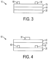
- FIG. 3 illustrates a third OTFT embodiment or configuration.
- the OTFT 10 comprises a substrate 20 which also acts as the gate electrode and is in contact with a dielectric layer 40 .
- the semiconducting layer 70 is placed over or on top of the dielectric layer 40 and separates it from the source and drain electrodes 50 and 60 .
- FIG. 4 illustrates a fourth OTFT embodiment or configuration.
- the OTFT 10 comprises a substrate 20 in contact with the source electrode 50 , drain electrode 60 , and the semiconducting layer 70 .
- the semiconducting layer 70 runs over and between the source and drain electrodes 50 and 60 .
- the dielectric layer 40 is on top of the semiconducting layer 70 .
- the gate electrode 30 is on top of the dielectric layer 40 and does not contact the semiconducting layer 70 .
- the semiconducting layer of the present disclosure comprises a semiconducting polymer and an insulating polymer.
- the addition of the insulating polymer provides several advantages, such as increasing the mobility, enhancing the flexibility, reducing the threshold voltage, and providing better saturation behavior.
- the semiconducting polymer is selected from the group consisting of polymers A to D: wherein R and R' are independently selected from hydrogen, alkyl or substituted alkyl containing from 1 to about 20 carbon atoms, a heteroatom-comprising group, and halogen; and n is a integer from about 3 to about 200.
- the semiconducting polymer is wherein R and R' are independently selected from alkyl or substituted alkyl containing from 1 to about 20 carbon atoms, a heteroatom-comprising group, and halogen; and n is a integer from about 3 to about 200.
- the semiconducting polymer is a regioregular polythiophene. In certain embodiments, the semiconducting polymer is highly crystalline. In specific embodiments, the semiconducting polymer has a crystallinity of greater than 50%. In further specific embodiments, the semiconducting polymer is a material that has a crystallinity of greater than 80%, or greater than 90%. Crystallinity can be determined by methods such as X-ray diffraction, e.g. carried out on neat polymer. It may be possible to carry out the deformation on the semiconductor layer.
- the semiconducting polymer may have a weight average molecular weight of from about 1,000 to about 80,000 Da, including from about 2,000 to about 50,000 Da. In specific embodiments, the semiconducting polymer has a weight average molecular weight of 50,000 Da or less.
- the semiconducting polymer has a polydispersity from about 1.2 to about 4.0, including from about 1.2 to about 2.0. In specific embodiments, the semiconducting polymer has a polydispersity of 1.8 or less.
- the semiconducting polymer may have a melting point of 100°C or higher. In additional embodiments, the semiconducting polymer has a melting point of 200°C or higher.
- the semiconducting layer may be formed by deposition of a semiconductor forming composition comprising a solvent, a crystalline semiconducting polymer, and an amorphous insulating polymer.
- the crystalline semiconducting polymer comprises from about 0.1 to about 5 wt% of the composition, preferably from about 0.1 to about 1 wt% of the composition.
- the amorphous insulating polymer comprises from about 0.01 to about 2.5 wt% of the composition, including from about 0.01 to about 1 wt%, or from about 0.02 to about 0.5 wt% of the composition.
- the composition has a viscosity of from about 1.5 centipoise to about 20 centipoise, including from about 2 centipoise to about 12 centipoise.
- the semiconductor composition usually has a low viscosity due to the use of low concentrations of semiconducting polymer. For printing or coating applications, a certain viscosity, for example at least 2 or at least 5 centipoise, is required.
- the addition of insulating polymer, particularly high molecular weight insulating polymer will increase the viscosity of semiconductor composition. In embodiments, the viscosity of the composition was enhanced by at least 50%, including at least 100%, compared to a similar composition lacking the insulating polymer.
- the solvent is selected from the group consisting of aromatic hydrocarbon such as toluene, xylene, mesitylene, chlorinated solvents such as dichloromethane, chloroform, chlorobenzene, dichlorobenzene, trichlorobenzene, chlorotoluene, and mixtures thereof.
- aromatic hydrocarbon such as toluene, xylene, mesitylene
- chlorinated solvents such as dichloromethane, chloroform, chlorobenzene, dichlorobenzene, trichlorobenzene, chlorotoluene, and mixtures thereof.
- the semiconducting layer may be from about 5 nm to about 1000 nm thick, preferably from about 10 nm to about 100 nm thick.
- the semiconducting layer can be formed by any suitable method. However, the semiconducting layer is generally formed from a liquid solution and then deposited onto the substrate of the transistor. Exemplary deposition methods include liquid deposition such as spin coating, dip coating, blade coating, rod coating, screen printing, stamping, ink jet printing, and the like, and other conventional processes known in the art. The solvent evaporates after deposition of the composition. In particular embodiments for forming the semiconductor layer, no thermal annealing is performed on the semiconductor layer.
- the semiconducting polymer has a high melting point of greater than 100°C, greater than 180°C, or greater than 200° C. Thermal annealing upon other layers of the transistor has no effect on the morphology of the semiconductor layer.
- the substrate may be composed of materials including but not limited to silicon, glass plate, plastic film or sheet.
- plastic substrate such as for example polyester, polycarbonate, polyimide sheets and the like may be used.
- the thickness of the substrate may be from about 10 ⁇ m to over 10 mm with an exemplary thickness being from about 50 ⁇ m to about 5 mm, especially for a flexible plastic substrate and from about 0.5 to about 10 mm for a rigid substrate such as glass or silicon.
- the gate electrode is composed of an electrically conductive material. It can be a thin metal film, a conducting polymer film, a conducting film made from conducting ink or paste or the substrate itself, for example heavily doped silicon.
- gate electrode materials include but are not restricted to aluminum, gold, silver, chromium, indium tin oxide, conductive polymers such as polystyrene sulfonate-doped poly(3,4-ethylenedioxythiophene) (PSS-PEDOT), and conducting ink/paste comprised of carbon black/graphite or silver colloids.
- the gate electrode can be prepared by vacuum evaporation, sputtering of metals or conductive metal oxides, conventional lithography and etching, chemical vapor deposition, spin coating, casting or printing, or other deposition processes.
- the thickness of the gate electrode ranges from about 10 to about 500 nm for metal films and from about 0.5 to about 10 ⁇ m for conductive polymers.
- the dielectric layer generally can be an inorganic material film, an organic polymer film, or an organic-inorganic composite film.
- inorganic materials suitable as the dielectric layer include silicon oxide, silicon nitride, aluminum oxide, barium titanate, barium zirconium titanate and the like.
- suitable organic polymers include polyesters, polycarbonates, poly(vinyl phenol), polyimides, polystyrene, polymethacrylates, polyacrylates, epoxy resin and the like.
- the thickness of the dielectric layer depends on the dielectric constant of the material used and can be, for example, from about 10 nm to about 500 nm.
- the dielectric layer may have a conductivity that is, for example, less than about 10-12 Siemens per centimeter (S/cm).
- the dielectric layer is formed using conventional processes known in the art, including those processes described in forming the gate electrode.
- Typical materials suitable for use as source and drain electrodes include those of the gate electrode materials such as gold, silver, nickel, aluminum, platinum, conducting polymers, and conducting inks.
- the electrode materials provide low contact resistance to the semiconductor.
- Typical thicknesses are about, for example, from about 40 nm to about 1 ⁇ m with a more specific thickness being about 100 to about 400 nm.
- the OTFT devices of the present disclosure contain a semiconductor channel.
- the semiconductor channel width may be, for example, from about 5 ⁇ m to about 5 mm with a specific channel width being about 100 ⁇ m to about 1 mm.
- the semiconductor channel length may be, for example, from about 1 ⁇ m to about 1 mm with a more specific channel length being from about 5 ⁇ m to about 100 ⁇ m.
- the source electrode is grounded and a bias voltage of, for example, about 0 volt to about 80 volts is applied to the drain electrode to collect the charge carriers transported across the semiconductor channel when a voltage of, for example, about +10 volts to about -80 volts is applied to the gate electrode.
- the electrodes may be formed or deposited using conventional processes known in the art.
- a barrier layer may also be deposited on top of the TFT to protect it from environmental conditions, such as light, oxygen and moisture, etc. which can degrade its electrical properties.
- Such barrier layers are known in the art and may simply consist of polymers.
- the resulting TFT has improved mobility, flexibility, threshold voltage, and saturation behavior.
- the transistor has a mobility of 0.25 cm 2 /V ⁇ sec or greater.
- the transistor has a threshold voltage of -10 V or greater.
- the transistor has both a mobility of 0.25 cm 2 /V ⁇ sec or greater and a threshold voltage of -10 V or greater.
- the transistor has a field effect mobility at least 10% higher than a transistor having the same semiconducting polymer but lacking the insulating polymer; in additional embodiments, the mobility is at least 25% higher.
- the flexibility of the semiconducting layer may also be improved by the addition of the insulating polymer.
- Crystalline semiconducting polymers may be too brittle to withstand the extensive bending and unbending stresses present in flexible OTFT devices.
- the insulating polymer particularly if it is amorphous, would improve the flexibility of the semiconducting layer. This improvement in flexibility can be measured by the yield point elongation of the semiconducting layer.
- the semiconducting layer has a yield point elongation at least 10% greater or at least 20% greater, than a semiconducting layer having the same semiconducting polymer but lacking the insulating polymer.
- the semiconducting layer has a yield point elongation equal to or greater than the yield point elongation of the gate dielectric layer. In still other embodiments, the semiconducting layer has a yield point elongation of from about 1% to about 25%, or from about 2% to about 10%. The yield point may be determined by forming a film of the material of the semiconductor layer and subjecting it to a tensile test, in conventional manner.
- the various components of the OTFT may be deposited upon the substrate in any order, as is seen in the Figures.
- the term "upon the substrate” should not be construed as requiring that each component directly contact the substrate.
- the term should be construed as describing the location of a component relative to the substrate.
- the gate electrode and the semiconducting layer should both be in contact with the dielectric layer.
- the source and drain electrodes should both be in contact with the semiconducting layer.
- the semiconducting polymer formed by the methods of the present disclosure may be deposited onto any appropriate component of an organic thin-film transistor to form a semiconducting layer of that transistor.
- n-doped silicon wafer with 200 nm silicon oxide was used as the substrate to fabricate OTFT devices, wherein the n-doped silicon functioned as the gate electrode and the silicon oxide as gate dielectric layer.
- the wafer surface was modified with a SAM silane interfacial layer by immersing the plasma-cleaned wafer into a 0.1 M dodecyltrichlorosilane solution in toluene at 60°C for 20 min.
- PBTBT-12 has the chemical structure shown below.
- the semiconductor solution was spin coated onto the above-modified wafer substrate at 1000 rpm for 90 seconds. After drying the solvent, gold source/drain electrodes were evaporated through a shadow mask on top of the semiconducting layer to complete the OTFT devices. For comparison, control devices without the polystyrene component were also made in a similar manner.
- the devices were characterized with a Keithley 4200-SCS instrument at ambient conditions in the dark.
- the devices with polystyrene additive showed a higher on-current and better saturation behavior.
- Mobility and threshold voltage data were extracted from transfer curves for more than 10 transistors and summarized in Table 1.
- the devices with polystyrene additive in the semiconducting layer showed a much higher mobility and smaller threshold voltages compared to the device without polystyrene.
- Table 1 Amount of polystyrene Mobility range (cm 2 /V ⁇ sec) Average Mobility (cm 2 /V ⁇ sec) Threshold Voltage (V) None 0.18-0.24 0.22 -11 10 wt% 0.25-0.34 0.28 -6
Landscapes
- Chemical & Material Sciences (AREA)
- Engineering & Computer Science (AREA)
- Materials Engineering (AREA)
- Composite Materials (AREA)
- Thin Film Transistor (AREA)
- Electroluminescent Light Sources (AREA)
Applications Claiming Priority (1)
| Application Number | Priority Date | Filing Date | Title |
|---|---|---|---|
| US12/101,945 US8049209B2 (en) | 2008-04-11 | 2008-04-11 | Thin-film transistors |
Publications (2)
| Publication Number | Publication Date |
|---|---|
| EP2109161A1 EP2109161A1 (en) | 2009-10-14 |
| EP2109161B1 true EP2109161B1 (en) | 2017-07-26 |
Family
ID=40679333
Family Applications (1)
| Application Number | Title | Priority Date | Filing Date |
|---|---|---|---|
| EP09154334.8A Active EP2109161B1 (en) | 2008-04-11 | 2009-03-04 | Thin-film transistors |
Country Status (3)
| Country | Link |
|---|---|
| US (2) | US8049209B2 (enExample) |
| EP (1) | EP2109161B1 (enExample) |
| JP (1) | JP5124520B2 (enExample) |
Families Citing this family (19)
| Publication number | Priority date | Publication date | Assignee | Title |
|---|---|---|---|---|
| US8212239B2 (en) | 2007-12-13 | 2012-07-03 | E I Du Pont De Nemours And Company | Electroactive materials |
| US8216753B2 (en) * | 2007-12-13 | 2012-07-10 | E I Du Pont De Nemours And Company | Electroactive materials |
| US8115200B2 (en) * | 2007-12-13 | 2012-02-14 | E.I. Du Pont De Nemours And Company | Electroactive materials |
| US8067764B2 (en) * | 2007-12-17 | 2011-11-29 | E. I. Du Pont De Nemours And Company | Electroactive materials |
| US8461291B2 (en) * | 2007-12-17 | 2013-06-11 | E I Du Pont De Nemours And Company | Organic electroactive materials and an organic electronic device having an electroactive layer utilizing the same material |
| US8304512B2 (en) * | 2010-01-19 | 2012-11-06 | Xerox Corporation | Benzodithiophene based materials compositions |
| US8643001B2 (en) * | 2010-12-23 | 2014-02-04 | Samsung Electronics Co. Ltd. | Semiconductor composition |
| US8742403B2 (en) | 2011-03-08 | 2014-06-03 | Samsung Electronics Co., Ltd. | Xanthene based semiconductor compositions |
| WO2012156500A1 (en) * | 2011-05-18 | 2012-11-22 | Université Libre de Bruxelles | Semiconducting compound for gas sensing |
| WO2013045014A1 (en) * | 2011-09-28 | 2013-04-04 | Merck Patent Gmbh | Conjugated polymers |
| US9881712B2 (en) * | 2012-07-20 | 2018-01-30 | Rohm And Haas Electronic Materials Llc | Highly crystalline electrically conducting polymers, methods of manufacture thereof and articles comprising the same |
| WO2014094965A2 (de) * | 2012-12-18 | 2014-06-26 | Merck Patent Gmbh | Emitter mit kondensiertem ringsystem |
| CN103151461A (zh) | 2013-02-27 | 2013-06-12 | 京东方科技集团股份有限公司 | 一种有机薄膜晶体管及其制备方法和制备装置 |
| US10600964B2 (en) | 2013-12-17 | 2020-03-24 | Rohm And Haas Electronic Materials Llc | Highly crystalline electrically conducting organic materials, methods of manufacture thereof and articles comprising the same |
| WO2016046659A1 (en) * | 2014-09-25 | 2016-03-31 | Basf Se | Ether-based polymers as photo-crosslinkable dielectrics |
| JP6562398B2 (ja) * | 2015-03-19 | 2019-08-21 | 三菱ケミカル株式会社 | 半導体デバイス、太陽電池、太陽電池モジュール、及び組成物 |
| JP6651606B2 (ja) * | 2016-03-16 | 2020-02-19 | 富士フイルム株式会社 | 有機半導体組成物、有機薄膜トランジスタの製造方法、及び有機薄膜トランジスタ |
| WO2019030382A1 (en) * | 2017-08-11 | 2019-02-14 | Merck Patent Gmbh | ORGANIC SEMICONDUCTOR POLYMER |
| GB2569637A (en) * | 2017-12-21 | 2019-06-26 | Sumitomo Chemical Co | Electronic device |
Family Cites Families (7)
| Publication number | Priority date | Publication date | Assignee | Title |
|---|---|---|---|---|
| US20030227014A1 (en) | 2002-06-11 | 2003-12-11 | Xerox Corporation. | Process for forming semiconductor layer of micro-and nano-electronic devices |
| CN101747493B (zh) * | 2003-10-28 | 2014-07-02 | 西巴特殊化学品控股有限公司 | 二酮基吡咯并吡咯聚合物 |
| US7300861B2 (en) * | 2004-06-24 | 2007-11-27 | Palo Alto Research Center Incorporated | Method for interconnecting electronic components using a blend solution to form a conducting layer and an insulating layer |
| EP1794218B1 (de) * | 2004-10-01 | 2020-05-13 | Merck Patent GmbH | Elektronische vorrichtungen enthaltend organische halbleiter |
| KR101130404B1 (ko) * | 2005-02-16 | 2012-03-27 | 삼성전자주식회사 | 고차가지형 고분자에 분산된 고유전율 절연체를 포함하는유기 절연체 조성물 및 이를 이용한 유기박막 트랜지스터 |
| CN100443483C (zh) | 2005-12-08 | 2008-12-17 | 中国科学院长春应用化学研究所 | 稠环单元封端的齐聚噻吩类高迁移率有机半导体材料及用途 |
| JP5121355B2 (ja) * | 2006-08-25 | 2013-01-16 | 住友化学株式会社 | 有機薄膜の製造方法 |
-
2008
- 2008-04-11 US US12/101,945 patent/US8049209B2/en active Active
-
2009
- 2009-03-04 EP EP09154334.8A patent/EP2109161B1/en active Active
- 2009-04-07 JP JP2009092899A patent/JP5124520B2/ja active Active
-
2011
- 2011-10-20 US US13/277,383 patent/US8293363B2/en active Active
Non-Patent Citations (1)
| Title |
|---|
| None * |
Also Published As
| Publication number | Publication date |
|---|---|
| JP5124520B2 (ja) | 2013-01-23 |
| US8049209B2 (en) | 2011-11-01 |
| US20120034736A1 (en) | 2012-02-09 |
| JP2009260340A (ja) | 2009-11-05 |
| US8293363B2 (en) | 2012-10-23 |
| EP2109161A1 (en) | 2009-10-14 |
| US20090256139A1 (en) | 2009-10-15 |
Similar Documents
| Publication | Publication Date | Title |
|---|---|---|
| EP2109161B1 (en) | Thin-film transistors | |
| US20060273303A1 (en) | Organic thin film transistors with multilayer electrodes | |
| WO2005006461A1 (en) | Field effect organic transistor | |
| EP2117059B1 (en) | Organic Thin Film Transistors | |
| US20080121869A1 (en) | Organic thin film transistor with dual layer electrodes | |
| US7928181B2 (en) | Semiconducting polymers | |
| US7872258B2 (en) | Organic thin-film transistors | |
| US7837903B2 (en) | Polythiophenes and electronic devices comprising the same | |
| US7928433B2 (en) | Electronic device comprising semiconducting polymers | |
| US8729222B2 (en) | Organic thin-film transistors | |
| US8134144B2 (en) | Thin-film transistor | |
| US8052895B2 (en) | Semiconducting ink formulation | |
| US8106387B2 (en) | Organic thin film transistors | |
| US7397086B2 (en) | Top-gate thin-film transistor | |
| EP2157628A2 (en) | Electronic device comprising semiconducting polymers |
Legal Events
| Date | Code | Title | Description |
|---|---|---|---|
| PUAI | Public reference made under article 153(3) epc to a published international application that has entered the european phase |
Free format text: ORIGINAL CODE: 0009012 |
|
| AK | Designated contracting states |
Kind code of ref document: A1 Designated state(s): AT BE BG CH CY CZ DE DK EE ES FI FR GB GR HR HU IE IS IT LI LT LU LV MC MK MT NL NO PL PT RO SE SI SK TR |
|
| AX | Request for extension of the european patent |
Extension state: AL BA RS |
|
| 17P | Request for examination filed |
Effective date: 20100414 |
|
| AKX | Designation fees paid |
Designated state(s): DE FR GB |
|
| 17Q | First examination report despatched |
Effective date: 20100719 |
|
| RAP1 | Party data changed (applicant data changed or rights of an application transferred) |
Owner name: SAMSUNG ELECTRONICS CO., LTD. |
|
| APBK | Appeal reference recorded |
Free format text: ORIGINAL CODE: EPIDOSNREFNE |
|
| APBN | Date of receipt of notice of appeal recorded |
Free format text: ORIGINAL CODE: EPIDOSNNOA2E |
|
| APBR | Date of receipt of statement of grounds of appeal recorded |
Free format text: ORIGINAL CODE: EPIDOSNNOA3E |
|
| APAV | Appeal reference deleted |
Free format text: ORIGINAL CODE: EPIDOSDREFNE |
|
| APAF | Appeal reference modified |
Free format text: ORIGINAL CODE: EPIDOSCREFNE |
|
| APBX | Invitation to file observations in appeal sent |
Free format text: ORIGINAL CODE: EPIDOSNOBA2E |
|
| APAQ | Information on invitation to file observation in appeal modified |
Free format text: ORIGINAL CODE: EPIDOSCOBA2E |
|
| APBZ | Receipt of observations in appeal recorded |
Free format text: ORIGINAL CODE: EPIDOSNOBA4E |
|
| APBT | Appeal procedure closed |
Free format text: ORIGINAL CODE: EPIDOSNNOA9E |
|
| GRAP | Despatch of communication of intention to grant a patent |
Free format text: ORIGINAL CODE: EPIDOSNIGR1 |
|
| INTG | Intention to grant announced |
Effective date: 20170322 |
|
| GRAS | Grant fee paid |
Free format text: ORIGINAL CODE: EPIDOSNIGR3 |
|
| GRAA | (expected) grant |
Free format text: ORIGINAL CODE: 0009210 |
|
| AK | Designated contracting states |
Kind code of ref document: B1 Designated state(s): DE FR GB |
|
| REG | Reference to a national code |
Ref country code: GB Ref legal event code: FG4D |
|
| REG | Reference to a national code |
Ref country code: DE Ref legal event code: R096 Ref document number: 602009047311 Country of ref document: DE |
|
| REG | Reference to a national code |
Ref country code: FR Ref legal event code: PLFP Year of fee payment: 10 |
|
| REG | Reference to a national code |
Ref country code: DE Ref legal event code: R097 Ref document number: 602009047311 Country of ref document: DE |
|
| PLBE | No opposition filed within time limit |
Free format text: ORIGINAL CODE: 0009261 |
|
| STAA | Information on the status of an ep patent application or granted ep patent |
Free format text: STATUS: NO OPPOSITION FILED WITHIN TIME LIMIT |
|
| 26N | No opposition filed |
Effective date: 20180430 |
|
| REG | Reference to a national code |
Ref country code: DE Ref legal event code: R079 Ref document number: 602009047311 Country of ref document: DE Free format text: PREVIOUS MAIN CLASS: H01L0051050000 Ipc: H10K0010000000 |
|
| P01 | Opt-out of the competence of the unified patent court (upc) registered |
Effective date: 20230530 |
|
| PGFP | Annual fee paid to national office [announced via postgrant information from national office to epo] |
Ref country code: DE Payment date: 20250214 Year of fee payment: 17 |
|
| PGFP | Annual fee paid to national office [announced via postgrant information from national office to epo] |
Ref country code: FR Payment date: 20250224 Year of fee payment: 17 |
|
| PGFP | Annual fee paid to national office [announced via postgrant information from national office to epo] |
Ref country code: GB Payment date: 20250213 Year of fee payment: 17 |