EP2107607A2 - High frequency semiconductor circuit device - Google Patents
High frequency semiconductor circuit device Download PDFInfo
- Publication number
- EP2107607A2 EP2107607A2 EP09250959A EP09250959A EP2107607A2 EP 2107607 A2 EP2107607 A2 EP 2107607A2 EP 09250959 A EP09250959 A EP 09250959A EP 09250959 A EP09250959 A EP 09250959A EP 2107607 A2 EP2107607 A2 EP 2107607A2
- Authority
- EP
- European Patent Office
- Prior art keywords
- microstrip line
- circuit device
- semiconductor circuit
- thickness
- region
- Prior art date
- Legal status (The legal status is an assumption and is not a legal conclusion. Google has not performed a legal analysis and makes no representation as to the accuracy of the status listed.)
- Withdrawn
Links
Images


Classifications
-
- H—ELECTRICITY
- H10—SEMICONDUCTOR DEVICES; ELECTRIC SOLID-STATE DEVICES NOT OTHERWISE PROVIDED FOR
- H10W—GENERIC PACKAGES, INTERCONNECTIONS, CONNECTORS OR OTHER CONSTRUCTIONAL DETAILS OF DEVICES COVERED BY CLASS H10
- H10W44/00—Electrical arrangements for controlling or matching impedance
- H10W44/20—Electrical arrangements for controlling or matching impedance at high-frequency [HF] or radio frequency [RF]
-
- H—ELECTRICITY
- H10—SEMICONDUCTOR DEVICES; ELECTRIC SOLID-STATE DEVICES NOT OTHERWISE PROVIDED FOR
- H10D—INORGANIC ELECTRIC SEMICONDUCTOR DEVICES
- H10D62/00—Semiconductor bodies, or regions thereof, of devices having potential barriers
- H10D62/10—Shapes, relative sizes or dispositions of the regions of the semiconductor bodies; Shapes of the semiconductor bodies
- H10D62/117—Shapes of semiconductor bodies
-
- H—ELECTRICITY
- H10—SEMICONDUCTOR DEVICES; ELECTRIC SOLID-STATE DEVICES NOT OTHERWISE PROVIDED FOR
- H10D—INORGANIC ELECTRIC SEMICONDUCTOR DEVICES
- H10D84/00—Integrated devices formed in or on semiconductor substrates that comprise only semiconducting layers, e.g. on Si wafers or on GaAs-on-Si wafers
- H10D84/01—Manufacture or treatment
-
- H—ELECTRICITY
- H10—SEMICONDUCTOR DEVICES; ELECTRIC SOLID-STATE DEVICES NOT OTHERWISE PROVIDED FOR
- H10D—INORGANIC ELECTRIC SEMICONDUCTOR DEVICES
- H10D84/00—Integrated devices formed in or on semiconductor substrates that comprise only semiconducting layers, e.g. on Si wafers or on GaAs-on-Si wafers
- H10D84/01—Manufacture or treatment
- H10D84/0123—Integrating together multiple components covered by H10D12/00 or H10D30/00, e.g. integrating multiple IGBTs
-
- H—ELECTRICITY
- H10—SEMICONDUCTOR DEVICES; ELECTRIC SOLID-STATE DEVICES NOT OTHERWISE PROVIDED FOR
- H10D—INORGANIC ELECTRIC SEMICONDUCTOR DEVICES
- H10D84/00—Integrated devices formed in or on semiconductor substrates that comprise only semiconducting layers, e.g. on Si wafers or on GaAs-on-Si wafers
- H10D84/01—Manufacture or treatment
- H10D84/02—Manufacture or treatment characterised by using material-based technologies
- H10D84/05—Manufacture or treatment characterised by using material-based technologies using Group III-V technology
-
- H—ELECTRICITY
- H10—SEMICONDUCTOR DEVICES; ELECTRIC SOLID-STATE DEVICES NOT OTHERWISE PROVIDED FOR
- H10W—GENERIC PACKAGES, INTERCONNECTIONS, CONNECTORS OR OTHER CONSTRUCTIONAL DETAILS OF DEVICES COVERED BY CLASS H10
- H10W44/00—Electrical arrangements for controlling or matching impedance
- H10W44/20—Electrical arrangements for controlling or matching impedance at high-frequency [HF] or radio frequency [RF]
- H10W44/203—Electrical connections
- H10W44/216—Waveguides, e.g. strip lines
Definitions
- the present invention relates to a semiconductor circuit device formed microstrip lines on a substrate and operating in a high frequency band.
- a microstrip line which is a fine metal line, has been used as a transmission line for connecting active devices to transmit a microwave in a microwave circuit formed on a dielectric substrate. Referring to FIGS. 7A and 7B , such a semiconductor circuit device will be described below.
- FIG. 7A is a top view illustrating the conventional semiconductor circuit device.
- FIG. 7B is a sectional view taken along the broken line A-A' in FIG. 7A .
- the conventional semiconductor circuit device includes at least two field effect transistors 103, 104 (hereinafter referred to as "FET(s)”) formed, as shown in FIG. 7A , on a GaAs substrate 102 having a conductor 101 over the entire rear face thereof.
- the conductor 101 has a fixed thickness as shown in FIG. 7B .
- a drain electrode 1031 of, for example, one FET 103 of the two FETs and a gate electrode 1041 of the other FET 104 are interconnected through a microstrip line 105.
- the microstrip line 105 is formed to be curved due to a restriction of device arrangement in a circuit pattern and a restriction of impedance matching with two FETs 103, 104.
- the characteristic impedance of the microstrip line 105 is determined by a length and a width of the microstrip line 104 and a thickness of the GaAs substrate 102.
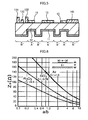
- FIG. 6 illustrates a relationship between the line width a, the substrate thickness b and the characteristic impedance Z 0 at a fixed line length.
- FIG. 6 shows that, as the line width a is narrower and the thickness b of the GaAs substrate 102 is thicker, the characteristic impedance Z 0 of the microstrip line 105 becomes higher. Further, although not illustrated in FIG. 6 , it has been known that, as the line length is longer, the characteristic impedance Z 0 becomes higher.
- the characteristic impedance Z 0 of the microstrip line 105 has been defined by mainly adjusting the line width a.
- attainment of the microstrip line 104 especially having a low impedance characteristic requires resolution of the following problems:
- the line width a has to be wide as shown in FIG. 6 .
- the length of the microstrip line 104 cannot be shortened due to the restrictions such as the device arrangement described above. Accordingly, the area occupied by the microstrip line 105 on a surface of the GaAs substrate 102 on which the microwave circuit is formed has become larger. Increasing the line width a of the microstrip line 105 in this way causes the problem that the size of the microwave circuit becomes larger. Further, when the line width a of the microstrip line 105 is increased, there is also a problem that the electric power of a microwave emitted from the microstrip line 105 to the open air increases.
- the part of the line where the line width is wide is only the vicinity of the junction with an active device and therefore enlargement of the microwave circuit resulting from increasing the line width can be restrained.
- attachment of a plurality of adjusting lines on the substrate is required, which disadvantageously results in that manufacture of the microwave circuit is difficult.
- the line width is wide even locally and therefore further miniaturization of the microwave circuit is difficult.
- a semiconductor circuit device including: a dielectric substrate; a plurality of active devices formed on the dielectric substrate; and a microstrip line formed on the dielectric substrate and electrically connecting the active devices, wherein a thickness of a first region of the dielectric substrate on which the microstrip line is formed is different from a thickness of a second region of the dielectric substrate on which the active devices are formed.
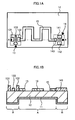
- FIG. 1A is a top view schematically illustrating a high frequency semiconductor circuit device with a microwave circuit according to a first embodiment of the present invention.
- FIG. 1B is a sectional view taken along a broken line A-A' in FIG. 1A .
- the microwave circuit in the semiconductor circuit device according to the first embodiment is formed on a GaAs substrate 12 having a conductor 11 on a rear face thereof.
- the microwave circuit includes, for example, two FETs 13, 14 functioning as active devices, and a microstrip line 15 connecting FET 13 to FET 14 each other.
- the FET 13 has a source electrode 131, a drain electrode 132 and a gate electrode 133.
- the FET 14 has a source electrode 141, a drain electrode 142 and a gate electrode 143.
- the microstrip line 15 connects, for example, the drain electrode 132 of the FET 13 to the gate electrode 143 of the FET 14 each other.
- Such a microstrip line 14 is made of, for example, Au.
- the thickness of a region A of the GaAs substrate 12 on which the microstrip line 15 is formed is thinner than the thickness of a region B of the GaAs substrate 12 on which FETs 13, 14 are formed.
- the characteristic impedance of the microstrip line 15 can be reduced without changing the length of the microstrip line 15. Accordingly, the line width of the microstrip line 14 can be narrower than a line with of a conventional microstrip line. Accordingly, when the line width of the microstrip line 14 is narrow in this way, the characteristic impedance of the microstrip line 14 sufficient to match an impedance of the FET 13 with an impedance of the FET 14 can be maintained.
- the microwave circuit can be miniaturized.
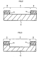
- a photosensitive resist is formed on the entire rear face of the GaAs substrate 12 and a resist mask 16 as shown in FIG. 2 is formed by patterning.
- the resist mask 16 has an opening in a region A in which the microstrip line 15 is formed on the GaAs substrate 11.
- a part of the GaAs substrate 11 is selectively removed by reactive ion etching (RIE) through the resist mask 16.
- RIE reactive ion etching
- the GaAs substrate 12 with partially different thickness as described in the present embodiment can be formed.
- FIG. 4A and FIG. 4B a second embodiment of the present invention will be described below.
- FIG. 4A is a top view schematically illustrating a high frequency semiconductor circuit device with a microwave circuit according to the second embodiment of the present invention.
- FIG. 4B is a sectional view taken along a broken line A-A' in FIG. 4A .
- the thickness of the region A of the GaAs substrate 12 on which the microstrip line 15 is formed is thicker than the thickness of the region B of the GaAs substrate 12 on which FETs 13, 14 are formed.
- a characteristic impedance of the microstrip line 15 can be increased without changing the width of the microstrip line 15. Accordingly, when a length of the microstrip line 15 is shortened, a characteristic impedance of the microstrip line 15 sufficient to match the impedance of the FET 13 with the impedance of the FET 14 can be maintained. In this case, since the line length can be shortened, the area occupied by the microstrip line 15 can be smaller than the area occupied by the conventional microstrip line. Accordingly, the microwave circuit can be miniaturized.
- the design for forming the microstrip line 15 is not limited by impedance matching, but limited by only device arrangement. Therefore, the flexibility in designing a circuit pattern can also be enhanced.
- the semiconductor circuit device according to the second embodiment is also excellent in the effect of radiating the heat generated at FETs 13, 14 because the thickness of the region B of the GaAs substrate 12 on which FETs 13, 14 are formed is thin.
- a manufacturing method for a GaAs substrate 11 in the semiconductor circuit device according to the second embodiment is essentially the same as that in the semiconductor circuit device according to the first embodiment and therefore detailed description thereof will not be repeated, but simple description will be made below.
- a resist mask having an opening in the region B of the GaAs substrate 11 and etching is performed using the resist to form the substrate 11.
- the thickness of the entire region A of the GaAs substrate 12 on which the microstrip line 15 is formed is different from the thickness of the region B of the GaAs substrate 12 on which FETs 13,14 are formed.
- the thickness of the region A of the GaAs substrate 12 may be adjusted along the shape of the microstrip line 14. Specifically, as shown in FIG. 5 which is a sectional view taken along the broken line A-A', the thickness of only a region A' with a microstrip line 15 formed on a surface of the GaAs substrate 12 is thinner than that of any other region B' with FETs 13, 14 formed on a surface of the GaAs substrate 12. In this case, the flexibility in designing the microstrip line 15 formed on the GaAs substrate 12 is enhanced.
- the GaAs substrate 12 is used as a dielectric substrate.
- any dielectric substrate which has conductivity and includes a dielectric with a dielectric constant of approximately 1 to 10, is applicable.
- Si or Al 2 O 3 is also applicable as the dielectric.
- microstrip line 15 made of Au may use any metal.
- an element to be connected is not limited to a FET.
- the present invention is applicable to a case where any of an active device, a passive device and a circuit including the active device and the passive device is required to be connected through a microstrip line for matching.
Landscapes
- Waveguides (AREA)
- Junction Field-Effect Transistors (AREA)
- Semiconductor Integrated Circuits (AREA)
Abstract

Description
- This application is based upon and claims the benefit of priority from the prior Japanese Patent Application No.
2008-091226 - The present invention relates to a semiconductor circuit device formed microstrip lines on a substrate and operating in a high frequency band.
- In a conventional semiconductor circuit device, a microstrip line, which is a fine metal line, has been used as a transmission line for connecting active devices to transmit a microwave in a microwave circuit formed on a dielectric substrate. Referring to
FIGS. 7A and 7B , such a semiconductor circuit device will be described below. -
FIG. 7A is a top view illustrating the conventional semiconductor circuit device.FIG. 7B is a sectional view taken along the broken line A-A' inFIG. 7A . - The conventional semiconductor circuit device includes at least two
field effect transistors 103, 104 (hereinafter referred to as "FET(s)") formed, as shown inFIG. 7A , on aGaAs substrate 102 having aconductor 101 over the entire rear face thereof. Theconductor 101 has a fixed thickness as shown inFIG. 7B . Adrain electrode 1031 of, for example, oneFET 103 of the two FETs and agate electrode 1041 of theother FET 104 are interconnected through amicrostrip line 105. - The
microstrip line 105 is formed to be curved due to a restriction of device arrangement in a circuit pattern and a restriction of impedance matching with twoFETs - The characteristic impedance of the
microstrip line 105 is determined by a length and a width of themicrostrip line 104 and a thickness of theGaAs substrate 102.FIG. 6 illustrates a relationship between the line width a, the substrate thickness b and the characteristic impedance Z0 at a fixed line length.FIG. 6 shows that, as the line width a is narrower and the thickness b of theGaAs substrate 102 is thicker, the characteristic impedance Z0 of themicrostrip line 105 becomes higher. Further, although not illustrated inFIG. 6 , it has been known that, as the line length is longer, the characteristic impedance Z0 becomes higher. - Conventionally, the characteristic impedance Z0 of the
microstrip line 105 has been defined by mainly adjusting the line width a. However, attainment of themicrostrip line 104 especially having a low impedance characteristic requires resolution of the following problems: - Specifically, in order to attain the low impedance characteristic, the line width a has to be wide as shown in
FIG. 6 . This is because the length of themicrostrip line 104 cannot be shortened due to the restrictions such as the device arrangement described above. Accordingly, the area occupied by themicrostrip line 105 on a surface of theGaAs substrate 102 on which the microwave circuit is formed has become larger. Increasing the line width a of themicrostrip line 105 in this way causes the problem that the size of the microwave circuit becomes larger. Further, when the line width a of themicrostrip line 105 is increased, there is also a problem that the electric power of a microwave emitted from themicrostrip line 105 to the open air increases. - Accordingly, to avoid the foregoing problems, there has been known a semiconductor circuit device in which a width of an effective microstrip line is increased by attaching a plurality of adjusting lines in parallel to the microstrip line in the vicinity of a junction point between the microstrip line and an active device and connecting the adjusting line to the microstrip line(Japanese Patent Application Laid-Open No.
1994-196950 - According to this semiconductor circuit device, the part of the line where the line width is wide is only the vicinity of the junction with an active device and therefore enlargement of the microwave circuit resulting from increasing the line width can be restrained. However, attachment of a plurality of adjusting lines on the substrate is required, which disadvantageously results in that manufacture of the microwave circuit is difficult. In addition, the line width is wide even locally and therefore further miniaturization of the microwave circuit is difficult.
- In addition, it has been known that only the region where FET is formed, the semiconductor substrate is thinly formed to improve discharge characteristics of FET (Japanese Patent Application Laid-Open No.
1993-235194 - It is one of the objects of the present invention to provide a high frequency semiconductor circuit device in which a microwave circuit on a substrate can be miniaturized.
- According to one aspect of the present invention, there is provided a semiconductor circuit device including: a dielectric substrate; a plurality of active devices formed on the dielectric substrate; and a microstrip line formed on the dielectric substrate and electrically connecting the active devices, wherein a thickness of a first region of the dielectric substrate on which the microstrip line is formed is different from a thickness of a second region of the dielectric substrate on which the active devices are formed.
-
-
FIG. 1A is a top view schematically illustrating a high frequency semiconductor circuit device according to a first embodiment of the present invention; -
FIG. 1B is a sectional view taken along a broken line A-A' inFIG. 1A ; -
FIG. 2 is a sectional view for illustrating a manufacturing method for the semiconductor circuit device according to the first embodiment of the present invention; -
FIG. 3 is a sectional view for illustrating a manufacturing method for the semiconductor circuit device according to the first embodiment of the present invention; -
FIG. 4A is a top view schematically illustrating the semiconductor circuit device according to the first embodiment of the present invention; -
FIG. 4B is a sectional view taken along a broken line A-A' inFIG. 4A ; -
FIG. 5 is a sectional view schematically illustrating a modified example of the semiconductor circuit device according to the first embodiment of the present invention; -
FIG. 6 is a view illustrating a relationship between a line width, a substrate thickness and a characteristic impedance at a fixed line length of a microstrip line; -
FIG. 7A is a top view schematically illustrating a conventional semiconductor circuit device; and -
FIG. 7B is a sectional view taken along a broken line A-A' inFIG. 7A . - Embodiments of the present invention will be described with reference to the accompanying drawings.
-
FIG. 1A is a top view schematically illustrating a high frequency semiconductor circuit device with a microwave circuit according to a first embodiment of the present invention.FIG. 1B is a sectional view taken along a broken line A-A' inFIG. 1A . - As shown in
FIG. 1B , the microwave circuit in the semiconductor circuit device according to the first embodiment is formed on aGaAs substrate 12 having aconductor 11 on a rear face thereof. - As shown in
FIG. 1A , the microwave circuit includes, for example, twoFETs microstrip line 15 connectingFET 13 toFET 14 each other. - The
FET 13 has asource electrode 131, adrain electrode 132 and agate electrode 133. Similarly, theFET 14 has asource electrode 141, adrain electrode 142 and agate electrode 143. Themicrostrip line 15 connects, for example, thedrain electrode 132 of theFET 13 to thegate electrode 143 of theFET 14 each other. Such amicrostrip line 14 is made of, for example, Au. - The thickness of a region A of the
GaAs substrate 12 on which themicrostrip line 15 is formed is thinner than the thickness of a region B of theGaAs substrate 12 on whichFETs - By thinning the thickness of the region A of the
GaAS substrate 12 on which themicrostrip line 15 is formed, the characteristic impedance of themicrostrip line 15 can be reduced without changing the length of themicrostrip line 15. Accordingly, the line width of themicrostrip line 14 can be narrower than a line with of a conventional microstrip line. Accordingly, when the line width of themicrostrip line 14 is narrow in this way, the characteristic impedance of themicrostrip line 14 sufficient to match an impedance of theFET 13 with an impedance of theFET 14 can be maintained. - As described above, since the line width of the
microstrip line 15 can be narrow, an area occupied by themicrostrip line 15 can be smaller than an area occupied by the conventional microstrip line. Accordingly, the microwave circuit can be miniaturized. - Referring next to
FIGS. 2 and 3 , description will be made on a manufacturing method for theGaAs substrate 11 with partially different thickness as described above. - First, a photosensitive resist is formed on the entire rear face of the
GaAs substrate 12 and a resistmask 16 as shown inFIG. 2 is formed by patterning. The resistmask 16 has an opening in a region A in which themicrostrip line 15 is formed on theGaAs substrate 11. - Next, as shown in
FIG. 3 , a part of theGaAs substrate 11 is selectively removed by reactive ion etching (RIE) through the resistmask 16. - Finally, by removing the resist
mask 16, theGaAs substrate 12 with partially different thickness as described in the present embodiment can be formed. - Referring next to
FIG. 4A and FIG. 4B , a second embodiment of the present invention will be described below. -
FIG. 4A is a top view schematically illustrating a high frequency semiconductor circuit device with a microwave circuit according to the second embodiment of the present invention.FIG. 4B is a sectional view taken along a broken line A-A' inFIG. 4A . - The semiconductor circuit device according to the second embodiment is different from the semiconductor circuit device according to the first embodiment in the following respects:
- The thickness of the region A of the
GaAs substrate 12 on which themicrostrip line 15 is formed is thicker than the thickness of the region B of theGaAs substrate 12 on whichFETs - By making thicker the thickness of the region A of the
GaAs substrate 12 on which themicrostrip line 15 is formed, a characteristic impedance of themicrostrip line 15 can be increased without changing the width of themicrostrip line 15. Accordingly, when a length of themicrostrip line 15 is shortened, a characteristic impedance of themicrostrip line 15 sufficient to match the impedance of theFET 13 with the impedance of theFET 14 can be maintained. In this case, since the line length can be shortened, the area occupied by themicrostrip line 15 can be smaller than the area occupied by the conventional microstrip line. Accordingly, the microwave circuit can be miniaturized. - The design for forming the
microstrip line 15 is not limited by impedance matching, but limited by only device arrangement. Therefore, the flexibility in designing a circuit pattern can also be enhanced. - The semiconductor circuit device according to the second embodiment is also excellent in the effect of radiating the heat generated at
FETs GaAs substrate 12 on whichFETs - A manufacturing method for a
GaAs substrate 11 in the semiconductor circuit device according to the second embodiment is essentially the same as that in the semiconductor circuit device according to the first embodiment and therefore detailed description thereof will not be repeated, but simple description will be made below. - According to the manufacturing method for the
GaAs substrate 11 in the semiconductor circuit device according to the second embodiment, a resist mask having an opening in the region B of theGaAs substrate 11 and etching is performed using the resist to form thesubstrate 11. - Embodiments of the present invention have been described above, but embodiments are not limited thereto, and various changes and modifications may be made in the present invention without any departure from the spirit and scope thereof.
- For example, in the above-described embodiments, the thickness of the entire region A of the
GaAs substrate 12 on which themicrostrip line 15 is formed is different from the thickness of the region B of theGaAs substrate 12 on whichFETs GaAs substrate 12 may be adjusted along the shape of themicrostrip line 14. Specifically, as shown inFIG. 5 which is a sectional view taken along the broken line A-A', the thickness of only a region A' with amicrostrip line 15 formed on a surface of theGaAs substrate 12 is thinner than that of any other region B' withFETs GaAs substrate 12. In this case, the flexibility in designing themicrostrip line 15 formed on theGaAs substrate 12 is enhanced. - In the respective embodiments, description has been made on a case where the
GaAs substrate 12 is used as a dielectric substrate. However, any dielectric substrate, which has conductivity and includes a dielectric with a dielectric constant of approximately 1 to 10, is applicable. For example, Si or Al2O3 is also applicable as the dielectric. - In the respective embodiments described above, description has been made on the
microstrip line 15 made of Au. However, themicrostrip line 15 may use any metal. - Further, in the respective embodiments described above, description has been made on a case where two
FETs
Claims (7)
- A high frequency semiconductor circuit device comprising:a dielectric substrate;a plurality of active devices formed on the dielectric substrate; anda microstrip line formed on the dielectric substrate and electrically connecting the active devices, whereina thickness of a first region of the dielectric substrate on which the microstrip line is formed is different from a thickness of a second region of the dielectric substrate on which the active devices are formed.
- The semiconductor circuit device according to claim 1, wherein the thickness of the entire first region is thinner than the thickness of the second region.
- The semiconductor circuit device according to claim 1, wherein the thickness of a part of the first region is thinner than the thickness of the second region.
- The semiconductor circuit device according to claim 1, wherein the thickness of the first region is thicker than the thickness of the second region.
- The semiconductor circuit device according to any preceding claim, wherein the active device is a field effect transistor.
- The semiconductor circuit device according to any preceding claim, wherein the dielectric substrate is made of any of GaAs, Si and Al2O3.
- The semiconductor circuit device according to any preceding claim, wherein the microstrip line is made of Au.
Applications Claiming Priority (1)
| Application Number | Priority Date | Filing Date | Title |
|---|---|---|---|
| JP2008091226A JP2009246157A (en) | 2008-03-31 | 2008-03-31 | High frequency band semiconductor device |
Publications (2)
| Publication Number | Publication Date |
|---|---|
| EP2107607A2 true EP2107607A2 (en) | 2009-10-07 |
| EP2107607A3 EP2107607A3 (en) | 2010-11-24 |
Family
ID=40758860
Family Applications (1)
| Application Number | Title | Priority Date | Filing Date |
|---|---|---|---|
| EP09250959A Withdrawn EP2107607A3 (en) | 2008-03-31 | 2009-03-30 | High frequency semiconductor circuit device |
Country Status (3)
| Country | Link |
|---|---|
| US (1) | US20090242988A1 (en) |
| EP (1) | EP2107607A3 (en) |
| JP (1) | JP2009246157A (en) |
Families Citing this family (1)
| Publication number | Priority date | Publication date | Assignee | Title |
|---|---|---|---|---|
| US9318450B1 (en) * | 2014-11-24 | 2016-04-19 | Raytheon Company | Patterned conductive epoxy heat-sink attachment in a monolithic microwave integrated circuit (MMIC) |
Citations (2)
| Publication number | Priority date | Publication date | Assignee | Title |
|---|---|---|---|---|
| JPH05235194A (en) | 1991-11-29 | 1993-09-10 | Nec Corp | Microwave monolithic integrated circuit |
| JPH06196950A (en) | 1992-12-25 | 1994-07-15 | Japan Energy Corp | Microwave circuit |
Family Cites Families (12)
| Publication number | Priority date | Publication date | Assignee | Title |
|---|---|---|---|---|
| US4069418A (en) * | 1976-03-02 | 1978-01-17 | The University Of Illinois Foundation | Detachable high-speed optoelectronic sampling head |
| US4030943A (en) * | 1976-05-21 | 1977-06-21 | Hughes Aircraft Company | Planar process for making high frequency ion implanted passivated semiconductor devices and microwave integrated circuits |
| JPS63222442A (en) * | 1987-03-11 | 1988-09-16 | Sharp Corp | High frequency integrated circuit |
| FR2631488B1 (en) * | 1988-05-10 | 1990-07-27 | Thomson Hybrides Microondes | PLANAR-TYPE INTEGRATED MICROWAVE CIRCUIT, COMPRISING AT LEAST ONE MESA COMPONENT, AND MANUFACTURING METHOD THEREOF |
| JPH04270502A (en) * | 1991-02-25 | 1992-09-25 | Mitsubishi Electric Corp | Semiconductor device |
| JPH06310547A (en) * | 1993-02-25 | 1994-11-04 | Mitsubishi Electric Corp | Semiconductor device and manufacture thereof |
| JP3189691B2 (en) * | 1996-07-10 | 2001-07-16 | 株式会社村田製作所 | High frequency semiconductor devices |
| WO1998012751A1 (en) * | 1996-09-20 | 1998-03-26 | Hitachi, Ltd. | High-frequency integrated circuit device and its manufacture |
| JP2000022457A (en) * | 1998-07-06 | 2000-01-21 | Fujitsu Ltd | Semiconductor device |
| JP2001267465A (en) * | 2000-03-21 | 2001-09-28 | Toshiba Corp | Semiconductor device |
| US7453143B2 (en) * | 2003-03-05 | 2008-11-18 | Banpil Photonics, Inc. | High speed electronics interconnect and method of manufacture |
| JP2006173595A (en) * | 2004-11-22 | 2006-06-29 | Matsushita Electric Ind Co Ltd | Semiconductor integrated circuit device and in-vehicle radar system using the same |
-
2008
- 2008-03-31 JP JP2008091226A patent/JP2009246157A/en not_active Abandoned
-
2009
- 2009-03-30 EP EP09250959A patent/EP2107607A3/en not_active Withdrawn
- 2009-03-30 US US12/414,116 patent/US20090242988A1/en not_active Abandoned
Patent Citations (2)
| Publication number | Priority date | Publication date | Assignee | Title |
|---|---|---|---|---|
| JPH05235194A (en) | 1991-11-29 | 1993-09-10 | Nec Corp | Microwave monolithic integrated circuit |
| JPH06196950A (en) | 1992-12-25 | 1994-07-15 | Japan Energy Corp | Microwave circuit |
Also Published As
| Publication number | Publication date |
|---|---|
| EP2107607A3 (en) | 2010-11-24 |
| US20090242988A1 (en) | 2009-10-01 |
| JP2009246157A (en) | 2009-10-22 |
Similar Documents
| Publication | Publication Date | Title |
|---|---|---|
| US6900482B2 (en) | Semiconductor device having divided active regions with comb-teeth electrodes thereon | |
| JP2012023212A (en) | Semiconductor device | |
| JP2005159157A (en) | Semiconductor device | |
| KR100300235B1 (en) | Input/output connecting structure applicable to a semiconductor device | |
| KR102549667B1 (en) | Semiconductor package with integrated harmonic termination feature | |
| US8466368B2 (en) | High-frequency device | |
| US9035469B2 (en) | Semiconductor device that controls a negative resistive oscillation and obtains a high amplification output | |
| JP2012182306A (en) | Package for mmic | |
| US20090242988A1 (en) | High frequency semiconductor circuit device | |
| US8125009B2 (en) | Mounting circuit substrate | |
| US9472497B2 (en) | Semiconductor device | |
| JPH11224911A (en) | High-frequency integrated circuit device | |
| US5898200A (en) | Microwave integrated circuit | |
| US9755313B2 (en) | Chip antenna for near field communication and method of manufacturing the same | |
| CN116169135A (en) | Transistor with odd-mode oscillation stabilization circuit | |
| KR102752888B1 (en) | Semiconductor devices including multiple power combining amplifiers having selectable input-output ports | |
| JPH11346105A (en) | Microwave planar circuit | |
| JP3839414B2 (en) | Resonant element and integrated circuit device | |
| JPH10200312A (en) | Microwave integrated circuit | |
| US20220293537A1 (en) | Semiconductor device and power amplifier | |
| JP5181424B2 (en) | High power amplifier | |
| JP4464104B2 (en) | Microwave integrated circuit | |
| JP2868939B2 (en) | Microwave amplifier | |
| JP4496176B2 (en) | Semiconductor input / output connection structure | |
| JP2025039260A (en) | Semiconductor Device |
Legal Events
| Date | Code | Title | Description |
|---|---|---|---|
| PUAI | Public reference made under article 153(3) epc to a published international application that has entered the european phase |
Free format text: ORIGINAL CODE: 0009012 |
|
| 17P | Request for examination filed |
Effective date: 20090406 |
|
| AK | Designated contracting states |
Kind code of ref document: A2 Designated state(s): AT BE BG CH CY CZ DE DK EE ES FI FR GB GR HR HU IE IS IT LI LT LU LV MC MK MT NL NO PL PT RO SE SI SK TR |
|
| AX | Request for extension of the european patent |
Extension state: AL BA RS |
|
| PUAL | Search report despatched |
Free format text: ORIGINAL CODE: 0009013 |
|
| AK | Designated contracting states |
Kind code of ref document: A3 Designated state(s): AT BE BG CH CY CZ DE DK EE ES FI FR GB GR HR HU IE IS IT LI LT LU LV MC MK MT NL NO PL PT RO SE SI SK TR |
|
| AX | Request for extension of the european patent |
Extension state: AL BA RS |
|
| STAA | Information on the status of an ep patent application or granted ep patent |
Free format text: STATUS: THE APPLICATION HAS BEEN WITHDRAWN |
|
| 18W | Application withdrawn |
Effective date: 20110516 |
|
| AKX | Designation fees paid |
Designated state(s): DE FR GB |