EP2107605A1 - Semiconductor device and fabrication method for the semiconductor device - Google Patents
Semiconductor device and fabrication method for the semiconductor device Download PDFInfo
- Publication number
- EP2107605A1 EP2107605A1 EP09250041A EP09250041A EP2107605A1 EP 2107605 A1 EP2107605 A1 EP 2107605A1 EP 09250041 A EP09250041 A EP 09250041A EP 09250041 A EP09250041 A EP 09250041A EP 2107605 A1 EP2107605 A1 EP 2107605A1
- Authority
- EP
- European Patent Office
- Prior art keywords
- cap layer
- semiconductor device
- protective film
- source electrode
- semiconductor substrate
- Prior art date
- Legal status (The legal status is an assumption and is not a legal conclusion. Google has not performed a legal analysis and makes no representation as to the accuracy of the status listed.)
- Withdrawn
Links
Images






Classifications
-
- H—ELECTRICITY
- H10—SEMICONDUCTOR DEVICES; ELECTRIC SOLID-STATE DEVICES NOT OTHERWISE PROVIDED FOR
- H10W—GENERIC PACKAGES, INTERCONNECTIONS, CONNECTORS OR OTHER CONSTRUCTIONAL DETAILS OF DEVICES COVERED BY CLASS H10
- H10W74/00—Encapsulations, e.g. protective coatings
- H10W74/10—Encapsulations, e.g. protective coatings characterised by their shape or disposition
- H10W74/111—Encapsulations, e.g. protective coatings characterised by their shape or disposition the semiconductor body being completely enclosed
- H10W74/124—Encapsulations, e.g. protective coatings characterised by their shape or disposition the semiconductor body being completely enclosed the encapsulations having cavities other than that occupied by chips
-
- H—ELECTRICITY
- H10—SEMICONDUCTOR DEVICES; ELECTRIC SOLID-STATE DEVICES NOT OTHERWISE PROVIDED FOR
- H10D—INORGANIC ELECTRIC SEMICONDUCTOR DEVICES
- H10D64/00—Electrodes of devices having potential barriers
- H10D64/20—Electrodes characterised by their shapes, relative sizes or dispositions
- H10D64/23—Electrodes carrying the current to be rectified, amplified, oscillated or switched, e.g. sources, drains, anodes or cathodes
- H10D64/251—Source or drain electrodes for field-effect devices
- H10D64/257—Source or drain electrodes for field-effect devices for lateral devices wherein the source or drain electrodes are characterised by top-view geometrical layouts, e.g. interdigitated, semi-circular, annular or L-shaped electrodes
-
- H—ELECTRICITY
- H10—SEMICONDUCTOR DEVICES; ELECTRIC SOLID-STATE DEVICES NOT OTHERWISE PROVIDED FOR
- H10W—GENERIC PACKAGES, INTERCONNECTIONS, CONNECTORS OR OTHER CONSTRUCTIONAL DETAILS OF DEVICES COVERED BY CLASS H10
- H10W20/00—Interconnections in chips, wafers or substrates
- H10W20/40—Interconnections external to wafers or substrates, e.g. back-end-of-line [BEOL] metallisations or vias connecting to gate electrodes
- H10W20/482—Interconnections external to wafers or substrates, e.g. back-end-of-line [BEOL] metallisations or vias connecting to gate electrodes for individual devices provided for in groups H10D8/00 - H10D48/00, e.g. for power transistors
- H10W20/484—Interconnections having extended contours, e.g. pads having mesh shape or interconnections comprising connected parallel stripes
-
- H—ELECTRICITY
- H10—SEMICONDUCTOR DEVICES; ELECTRIC SOLID-STATE DEVICES NOT OTHERWISE PROVIDED FOR
- H10W—GENERIC PACKAGES, INTERCONNECTIONS, CONNECTORS OR OTHER CONSTRUCTIONAL DETAILS OF DEVICES COVERED BY CLASS H10
- H10W74/00—Encapsulations, e.g. protective coatings
- H10W74/10—Encapsulations, e.g. protective coatings characterised by their shape or disposition
- H10W74/111—Encapsulations, e.g. protective coatings characterised by their shape or disposition the semiconductor body being completely enclosed
- H10W74/121—Encapsulations, e.g. protective coatings characterised by their shape or disposition the semiconductor body being completely enclosed by multiple encapsulations, e.g. by a thin protective coating and a thick encapsulation
-
- H—ELECTRICITY
- H10—SEMICONDUCTOR DEVICES; ELECTRIC SOLID-STATE DEVICES NOT OTHERWISE PROVIDED FOR
- H10D—INORGANIC ELECTRIC SEMICONDUCTOR DEVICES
- H10D64/00—Electrodes of devices having potential barriers
- H10D64/20—Electrodes characterised by their shapes, relative sizes or dispositions
- H10D64/23—Electrodes carrying the current to be rectified, amplified, oscillated or switched, e.g. sources, drains, anodes or cathodes
- H10D64/251—Source or drain electrodes for field-effect devices
- H10D64/256—Source or drain electrodes for field-effect devices for lateral devices wherein the source or drain electrodes are recessed in semiconductor bodies
Definitions
- the present invention relates to a semiconductor device and a fabrication method for the semiconductor device.
- the present invention relates to a semiconductor device and a fabrication method for the semiconductor device provided with a package of a wafer level, in a package of a high frequency semiconductor device.
- packaging is achieved by placing a semiconductor device, a matching circuit, etc. in the housing composed of metal, ceramics, etc.
- Patent Document 1
- Patent Document 2
- a semiconductor device comprises a semiconductor substrate; a field effect transistor comprising a gate electrode, a drain electrode, and a source electrode which are formed on the semiconductor substrate; and a hollow protective film provided on the semiconductor substrate so that an inner surface bonds to an upper surface of the drain electrode and the source electrode of the field effect transistor.
- a semiconductor device comprises a semiconductor substrate; a field effect transistor comprising a gate electrode, a drain electrode, and a source electrode which are formed on the semiconductor substrate; and a hollow protective film provided on the semiconductor substrate so that an inner surface bonds to an upper surface of the source electrode of the field effect transistor.
- a semiconductor device comprises a semiconductor substrate; a field effect transistor comprising a gate electrode, a drain electrode, and a source electrode which are formed on the semiconductor substrate; and a hollow protective film provided on the semiconductor substrate so that an inner surface bonds to an upper surface of the drain electrode of the field effect transistor.
- a fabrication method for a semiconductor device comprises forming a gate electrode, a drain electrode, and a source electrode on a semiconductor substrate, and forming a field effect transistor; and forming a hollow protective film on the semiconductor substrate so that an inner surface bonds to an upper surface of one or both of the drain electrode and the source electrode of the field effect transistor.
- a semiconductor device and a fabrication method for the semiconductor device which could strengthen the mechanical strength of the protective film and with which packaging of the wafer level with electric high reliability is performed can be provided.
- a schematic plane pattern configuration of a semiconductor device according to a first embodiment of the present invention is expressed as shown in Fig. 1 .
- a schematic section structure explaining one process of a fabrication method of the semiconductor device according to the first embodiment is expressed as shown in Fig. 2 and Fig. 3 .
- the semiconductor device includes a semiconductor substrate 4A, a field effect transistor 4, and a hollow protective film 5, as shown in Fig. 1 to Fig. 3 .
- the field effect transistor 4 includes a gate electrode 1, a drain electrode 2, and a source electrode 3 which are formed on the semiconductor substrate.
- the hollow protective film 5 is provided on the semiconductor substrate 4A so that an inner surface may bond to an upper surface of the drain electrode 2 and the source electrode 3 of the field effect transistor 4.
- the hollow protective film 5 includes a first cap layer 7 contacting the drain electrode 2 and the source electrode 3, and a second cap layer 10 placed on the first cap layer 7.
- the hollow protective film 5 further includes a third cap layer 11 placed on the second cap layer 10.
- the first cap layer 7 and the second cap layer 10 can be composed by an insulating film, for example, can be composed by a silicon dioxide film (SiO 2 film).
- the third cap layer 11 can be composed by an insulating film, for example, can be composed by a silicon nitride film (SiN film).
- the field effect transistor 4 includes the hollow protective film 5, and the field effect transistor 4 including the gate electrode 1, the drain electrode 2, and the source electrode 3 is formed on the semiconductor substrate 4A.
- the hollow protective film 5 is provided on the semiconductor substrate 4A so that the polar zone composed of the gate electrode 1, the drain electrode 2, and the source electrode 3 of this field effect transistor 4 may be covered.
- the hollow protective film 5 is provided so that the inner surface may bond to the upper surface of the drain electrode 2 and the source electrode 3.
- the fabrication method of the semiconductor device includes: the step of forming the gate electrode 1, the drain electrode 2, and the source electrode 3 on the semiconductor substrate 4A, thereby forming the field effect transistor 4; and the step of forming the hollow protective film 5 on the semiconductor substrate 4A so that the inner surface may bond to the upper surface of one or both of the drain electrode 2, and the source electrode 3 of the field effect transistor 4, as shown in Fig. 1 to Fig. 3 .
- the step of forming the hollow protective film 5 includes: the step of forming the sacrifice layer 6 on the gate electrode 1 and the semiconductor substrate 4A except for the drain electrode 2 and the source electrode 3; the step of forming the first cap layer 7 contacting the upper surface of one or both of the drain electrode 2 and the source electrode 3; the step of forming an opening 12 in the edge of the first cap layer 7; the step of sending oxygen plasma through the opening 12, and gasifying and removing the sacrifice layer 6 by an oxygen plasma asher, and forming the hollow unit 9; and the step of forming the second cap layer 10 on the first cap layer 7, and sealing the opening 12.
- the step of forming the hollow protective film 5 may further include the step of forming the third cap layer 11 on the second cap layer 10.
- the hollow protective film 5 which laminates the first cap layer 7, second cap layer 10, and third cap layer 11 is formed.
- the first cap layer 7 that is an innermost (lowest) layer of this hollow protective film 5 contacts the upper surface of the drain electrode 2 and the source electrode 3. For this reason, since the drain electrode 2 and the source electrode 3 may support the hollow protective film 5 from that inner side, the mechanical intensity of the hollow protective film 5 is reinforced.
- the third cap layer 11 may be sufficient as the third cap layer 11.
- the second cap layer 10 is provided with sufficient airtightness and moisture resistance, there may not be the third cap layer 11.
- the hollow protective film 5 formed in this way has composition which the electrodes except active gate electrode 1 electrically, i.e., the drain electrode 2, and the source electrodes 3, supports as a support unit, the mechanical strength of the hollow protective film 5 does not become weaker even if the volume of the hollow sections becomes large, and the bad influence of electrical characteristics is also eliminated.
- FIG. 4 A detailed schematic plane pattern configuration of the semiconductor device according to the first embodiment is expressed as shown in Fig. 4 .
- the opening 12 which is not shown in Fig. 2 to Fig. 3 , is shown in the periphery of the hollow protective film 5. Since this opening 12 is formed toward the first cap layer 7 on the fabricating process and is sealed by the subsequent fabricating process of the second cap layer 10, this opening 12 is shown by the dotted line.
- a detailed schematic plane pattern configuration of a semiconductor device according to a modified example 1 of the first embodiment is an example by which a plurality of openings 12 are placed at the periphery of the hollow protective film 5, and other configurations are the same as that of the first embodiment.
- oxygen plasma is sendable through the opening 12
- the sacrifice layer 6 can be gasified and removed by an oxygen plasma asher, and the processing time of the step of forming the hollow part 9 can be shortened.
- a detailed schematic plane pattern configuration of a semiconductor device according to a modified example 2 of the first embodiment is an example by which the openings 12 are placed at rectangle stripe shape at the periphery of the hollow protective film 5, and other configurations are the same as that of the first embodiment.
- the schematic section structure of the semiconductor device according to the modified examples 2 to 3 of the first embodiment includes a semiconductor substrate 4A, a field effect transistor 4, and a hollow protective film 5, as shown in Fig. 7 .
- the field effect transistor 4 has a gate electrode 1, a drain electrode 2, and a source electrode 3 which are formed on the semiconductor substrate 4A.
- the hollow protective film 5 is provided on the semiconductor substrate 4A so that an inner surface may bond to the upper surface of the drain electrode 2 and the source electrode 3 of the field effect transistor 4.
- the hollow protective film 5 includes a first cap layer 7 contacting the drain electrode 2 and the source electrode 3, and a second cap layer 10 placed on the first cap layer 7.
- the hollow protective film 5 further includes a third cap layer 11 placed on the second cap layer 10.
- the opening 12 is formed in the first cap layer 7 in the periphery of the hollow protective film 5, the sacrifice layer 6 is gasified and removed by an oxygen plasma asher through this opening 12, and the opening 12 is sealed by the second cap layer 10 in the sealed part 12A after forming the hollow part 9.
- the hollow protective film 5 is supported by the drain electrode 2 and the source electrode 3 as a support unit according to the first embodiment, even if the volume of hollow sections becomes large, the mechanical strength of the hollow protective film 5 does not become weaker. Moreover, reliable semiconductor device can be obtained without receiving the electrical influence from others in the process in which the hollow protective film 5 is formed, since the electrodes 2 except active gate electrode 1 electrically, i.e., the drain electrode, and the source electrodes 3 are applied as the support unit.
- a schematic plane pattern configuration of a semiconductor device according to a second embodiment of the present invention is similarly expressed as Fig. 1 or Fig. 4 to Fig. 6 .
- a schematic section structure of the semiconductor device according to the second embodiment is expressed as shown in Fig. 8 .
- the semiconductor device includes a semiconductor substrate 4A, a field effect transistor 4, and a hollow protective film 5, as shown in Fig. 4 to Fig. 6 , and Fig. 8 .
- the field effect transistor 4 has a gate electrode 1, a drain electrode 2, and a source electrode 3 which are formed on the semiconductor substrate 4A.
- the hollow protective film 5 is provided on the semiconductor substrate 4A so that an inner surface may bond to the upper surface of the source electrode 3 of the field effect transistor 4.
- the hollow protective film 5 includes a first cap layer 7 contacting the source electrode 3, and a second cap layer 10 placed on the first cap layer 7.
- the hollow protective film 5 further includes a third cap layer 11 paced on the second cap layer 10.
- the first cap layer 7 and the second cap layer 10 can compose an insulating film, for example, can be composed by a silicon dioxide film.
- the third cap layer 11 can compose an insulating film, for example, can be composed by a silicon nitride film.
- the opening 12 is formed in the first cap layer 7 in the periphery of the hollow protective film 5, the sacrifice layer 6 is gasified and removed by an oxygen plasma asher through this opening 12, and the opening 12 is sealed by the second cap layer 10 in the sealed part 12A after forming the hollow part 9.
- the hollow protective film 5 is supported by the source electrode 3 as a support unit according to the second embodiment, even if the volume of hollow sections becomes large, the mechanical strength of the hollow protective film 5 does not become weaker. Moreover, a reliable semiconductor device can be obtained without receiving the electrical influence from others in the process in which the hollow protective film 5 is formed, since the electrodes 2 except active gate electrode 1 electrically, i.e., the source electrodes 3 is applied as the support unit.
- a detailed schematic section structure of a semiconductor device according to amodified example 1 of the second embodiment is not a configuration whose the first cap layer 7 contacts all the source electrodes 3 but a configuration placed so that the source electrode 3 placed at stripe shape may be contacted by every other one for example, as shown in Fig. 9 .
- the opening 12 is formed in the first cap layer 7 in the periphery of the hollow protective film 5, the sacrifice layer 6 is gasified and removed by an oxygen plasma asher through this opening 12, and the opening 12 is sealed by the second cap layer 10 in the sealed part 12A after forming the hollow part 9.
- the first cap layer 7 may be placed so that the source electrode 3 placed at stripe shape may be contacted by every two for example. Or the first cap layer 7 may be provided with the configuration which contacts the source electrode 3 at random.
- the hollow protective film 5 is supported by the source electrode 3 as a support unit according to the modified example 1 of the second embodiment, even if the volume of hollow sections becomes large, the mechanical strength of the hollow protective film 5 does not become weaker. Moreover, a reliable semiconductor device can be obtained without receiving the electrical Influence from others in the process in which the hollow protective film 5 is formed, since the electrodes 2 except active gate electrode 1 electrically, i.e., the source electrodes 3 are applied as the support unit.
- a detailed schematic section structure of a semiconductor device according to a modified example 2 of the second embodiment has the characteristic at the point that the first cap layer 70 is composed of a metal layer, as shown in Fig. 10 .
- Aluminum can compose the first cap layer 70, for example.
- the opening 70 is formed in the first cap layer 7 in the periphery of the hollow protective film 5, the sacrifice layer 6 is gasified and removed by an oxygen plasma asher through this opening 12, and the opening 12 is sealed by the second cap layer 10 in the sealed part 12A after forming the hollow part 9.
- the first cap layer 70 formed by a metal layer is connected to the source electrode 3, a shielding effect is obtained and a stable semiconductor device is provided electrically by applying potential of the first cap layer 70 into earth potentials.
- the hollow protective film 5 is supported by the source electrode 3 as a support unit according to the modified example 2 of the second embodiment, even if the volume of hollow sections becomes large, the mechanical strength of the hollow protective film 5 does not become weaker. Moreover, a reliable semiconductor device can be obtained without receiving the electrical influence from others in the process in which the hollow protective film 5 is formed, since the electrodes 2 except active gate electrode 1 electrically, i.e., the source electrodes 3 are applied as the support unit.
- a detailed schematic section structure of a semiconductor device according to a modified example 3 of the second embodiment has the characteristic in the point that the first cap layer 70 is composed of a metal layer, and the source electrode 3 placed at stripe shape may be contacted every other one for example, instead of the configuration which contacts all the source electrodes 3.
- the opening 70 is formed in the first cap layer 7 in the periphery of the hollow protective film 5, the sacrifice layer 6 is gasified and removed by an oxygen plasma asher through this opening 12, and the opening 12 is sealed by the second cap layer 10 in the sealed part 12A after forming the hollow part 9.
- the first cap layer 70 may be placed so that the source electrode 3 placed at stripe shape may be contacted by every two for example. Or the first cap layer 70 may be provided with the configuration which contacts the source electrode 3 at random.
- the first cap layer 70 formed by a metal layer is connected to the source electrode 3, a shielding effect is obtained and a stable semiconductor device is provided electrically by applying potential of the first cap layer 70 into earth potentials.
- the hollow protective film 5 is supported by the source electrode 3 as a support unit according to the modified example 3 of the second embodiment, even if the volume of hollow sections becomes large, the mechanical strength of the hollow protective film 5 does not become weaker. Moreover, a reliable semiconductor device can be obtained without receiving the electrical influence from others in the process in which the hollow protective film 5 is formed, since the electrodes 2 except active gate electrode 1 electrically, i.e., the source electrodes 3 is applied as the support unit.
- a schematic plane pattern configuration of a semiconductor device according to a third embodiment of the present invention is similarly expressed as Fig. 1 or Fig. 4 to Fig. 6 .
- a schematic section structure of the semiconductor device according to the third embodiment is expressed as shown in Fig. 12 .
- the semiconductor device includes a semiconductor substrate 4A, a field effect transistor 4, and a hollow protective film 5, as shown in Fig. 4 to Fig. 6 , and Fig. 12 .
- the field effect transistor 4 has a gate electrode 1, a drain electrode 2, and a source electrode 3 which are formed on the semiconductor substrate 4A.
- the hollow protective film 5 is provided on the semiconductor substrate 4A so that an inner surface may bond to the upper surface of the drain electrode 2 of the field effect transistor 4.
- the hollow protective film 5 includes a first cap layer 7 contacting the drain electrode 2, and a second cap layer 10 placed on the first cap layer 7.
- the hollow protective film 5 further includes a third cap layer 11 placed on the second cap layer 10.
- the first cap layer 7 and the second cap layer 10 can compose an insulating film, for example, can be composed by a silicon dioxide film.
- the third cap layer 11 can compose an insulating film, for example, can be composed by a silicon nitride film.
- the opening 12 is formed in the first cap layer 7 in the periphery of the hollow protective film 5, the sacrifice layer 6 is gasified and removed by an oxygen plasma asher through this opening 12, and the opening 12 is sealed by the second cap layer 10 in the sealed part 12A after forming the hollow part 9.
- the first cap layer 7 may be placed so that the drain electrode 2 placed at stripe shape may be contacted by every two for example. Or the first cap layer 7 may be provided with the configuration which contacts the drain electrode 2 at random.
- the hollow protective film 5 is supported by the drain electrode 2 as a support unit according to the third embodiment, even if the volume of hollow sections becomes large, the mechanical strength of the hollow protective film 5 does not become weaker. Moreover, a reliable semiconductor device can be obtained without receiving the electrical influence from others in the process in which the hollow protective film 5 is formed, since the electrodes 2 except active gate electrode 1 electrically, i.e., the drain electrode is applied as the support unit.
- a semiconductor device has a wide range of application fields, such as an internally matched power amplifier, a power MMIC (Monolithic Microwave Integrated Circuit), a microwave power amplifier, a millimeter-wave power amplifier, and a high frequency MEMS (Micro Electro Mechanical Systems) device.
- a power MMIC Monolithic Microwave Integrated Circuit
- microwave power amplifier a microwave power amplifier
- millimeter-wave power amplifier a millimeter-wave power amplifier
- a high frequency MEMS Micro Electro Mechanical Systems
Landscapes
- Junction Field-Effect Transistors (AREA)
- Internal Circuitry In Semiconductor Integrated Circuit Devices (AREA)
- Insulated Gate Type Field-Effect Transistor (AREA)
Abstract
Description
- The present invention relates to a semiconductor device and a fabrication method for the semiconductor device. In particular, the present invention relates to a semiconductor device and a fabrication method for the semiconductor device provided with a package of a wafer level, in a package of a high frequency semiconductor device.
- In a field effect transistor applied to a high frequency semiconductor device, in order to keep airtightness, packaging is achieved by placing a semiconductor device, a matching circuit, etc. in the housing composed of metal, ceramics, etc.
- However, the cost concerning the housing of this package was large, and this had become an obstacle of low-pricing in the cost aspect of the semiconductor device. Moreover, in potting by resin etc., the problem that gain reduction occurred by the increase in capacity of an active gate electrode electrically etc. had occurred.
- As technology for solving this problem, a wafer level packaging which can keep the airtightness to the semiconductor device itself with a hollow protective film, and can reduce the capacity of a gate electrode is developed and filed as patent application by the present applicant (Japanese Patent Application No.
P2008-013721 - However, since the volume of hollow sections was large in order to wrap an active part of the field effect transistor by using this technology, there was a problem that it is anxious about the mechanical strength of the protective film.
- On the other hand, in order to reduce the increase in the capacity by a passivation film, a semiconductor device and a fabrication method for the semiconductor device. which provides a hollow area between the passivation film and a metal electrode which a high frequency signal outputs and inputs, are already disclosed (for example, refer to Patent Document 1).
- On the other hand, a semiconductor device and a fabrication method for the semiconductor device which reduces the parasitic capacitance between a source electrode or a drain electrode, and a gate electrode, and improves high frequency characteristics by removing an insulating film under the eaves of the gate electrode toward a mold are already disclosed (for example, refer to Patent Document 2).
- Japanese Patent Application Laying-Open Publication No.
H06-140440 - Japanese Patent Application Laying-Open Publication No.
H11-354540 - According to an aspect of the invention, a semiconductor device comprises a semiconductor substrate; a field effect transistor comprising a gate electrode, a drain electrode, and a source electrode which are formed on the semiconductor substrate; and a hollow protective film provided on the semiconductor substrate so that an inner surface bonds to an upper surface of the drain electrode and the source electrode of the field effect transistor.
- According to another aspect of the invention, a semiconductor device comprises a semiconductor substrate; a field effect transistor comprising a gate electrode, a drain electrode, and a source electrode which are formed on the semiconductor substrate; and a hollow protective film provided on the semiconductor substrate so that an inner surface bonds to an upper surface of the source electrode of the field effect transistor.
- According to another aspect of the invention, a semiconductor device comprises a semiconductor substrate; a field effect transistor comprising a gate electrode, a drain electrode, and a source electrode which are formed on the semiconductor substrate; and a hollow protective film provided on the semiconductor substrate so that an inner surface bonds to an upper surface of the drain electrode of the field effect transistor.
- According to another aspect of the invention, a fabrication method for a semiconductor device comprises forming a gate electrode, a drain electrode, and a source electrode on a semiconductor substrate, and forming a field effect transistor; and forming a hollow protective film on the semiconductor substrate so that an inner surface bonds to an upper surface of one or both of the drain electrode and the source electrode of the field effect transistor.
- According to the present invention, a semiconductor device and a fabrication method for the semiconductor device which could strengthen the mechanical strength of the protective film and with which packaging of the wafer level with electric high reliability is performed can be provided.
-
-
Fig. 1 is a schematic plane pattern configuration diagram showing a semiconductor device according to a first embodiment of the present invention. -
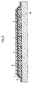
Fig. 2 is a schematic cross-sectional configuration chart explaining one process of a fabrication method of the semiconductor device according to the first embodiment of the present invention. -
Fig. 3 is a schematic cross-sectional configuration chart explaining one process of the fabrication method of the semiconductor device according to the first embodiment of the present invention. -
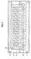
Fig. 4 is a detailed schematic plane pattern configuration diagram showing the semiconductor device according to the first embodiment of the present invention. -
Fig. 5 is a detailed schematic plane pattern configuration diagram showing a semiconductor device according to a modified example 1 of the first embodiment of the present invention. -
Fig. 6 is a detailed schematic plane pattern configuration diagram showing a semiconductor device according to a modified example 2 of the first embodiment of the present invention. -
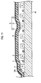
Fig. 7 is a schematic cross section configuration diagram showing a semiconductor device according to a modified example 3 of the first embodiment of the present invention. -
Fig. 8 is a schematic cross section configuration diagram showing a semiconductor device according to a second embodiment of the present invention. -
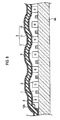
Fig. 9 is a schematic cross section configuration diagram showing a semiconductor device according to a modified example 1 of the second embodiment of the present invention. -
Fig. 10 is a schematic cross section configuration diagram showing a semiconductor device according to a modified example 2 of the second embodiment of the present invention. -
Fig. 11 is a schematic cross section configuration diagram showing a semiconductor device according to a modified example 3 of the second embodiment of the present invention. -
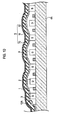
Fig. 12 is a schematic cross section configuration diagram of a semiconductor device according to a third embodiment of the present invention. - Various embodiments of the present invention will be described with reference to the accompanying drawings. It is to be noted that the same or similar reference numerals are applied to the same or similar parts and elements throughout the drawings, and the description of the same or similar parts and elements will be omitted or simplified. Generally, and as is in the representation of the cross-sectional diagram, it will be appreciated that the various drawings are not drawn to scale from one figure to another nor inside a given figure, and in particular that the circuit diagrams are arbitrarily drawn for facilitating the reading of the drawings. In the following descriptions, numerous specific details are set forth such as specific material layers, etc. to provide a thorough understanding of the present invention. However, it will be obvious to those skilled in the art that the present invention may be practiced without such specific details. In other instances, the material layers well- known have been shown in the cross-sectional diagrams form in order to not obscure the present invention with unnecessary detail. Drawings are schematic, not actual, and may be inconsistent in between in scale, ratio, etc.
- The embodiments shown below exemplify a semiconductor device that are used to implement the technical ideas according to the present invention, and do not limit the technical ideas according to the present invention to those that appear below. These technical ideas, according to the present invention, may receive a variety of modifications that fall within the claims.
- The embodiment shown in the following exemplifies the device and method for materializing the technical idea of this invention, and this embodiment of the invention does not specify assignment of each component parts, etc. as the following. This embodiment of the invention can add various change in scope of claims.
- A schematic plane pattern configuration of a semiconductor device according to a first embodiment of the present invention is expressed as shown in
Fig. 1 . A schematic section structure explaining one process of a fabrication method of the semiconductor device according to the first embodiment is expressed as shown inFig. 2 andFig. 3 . - The semiconductor device according to the first embodiment includes a
semiconductor substrate 4A, afield effect transistor 4, and a hollowprotective film 5, as shown inFig. 1 to Fig. 3 . Thefield effect transistor 4 includes a gate electrode 1, adrain electrode 2, and asource electrode 3 which are formed on the semiconductor substrate. The hollowprotective film 5 is provided on thesemiconductor substrate 4A so that an inner surface may bond to an upper surface of thedrain electrode 2 and thesource electrode 3 of thefield effect transistor 4. - The hollow
protective film 5 includes afirst cap layer 7 contacting thedrain electrode 2 and thesource electrode 3, and asecond cap layer 10 placed on thefirst cap layer 7. - The hollow
protective film 5 further includes athird cap layer 11 placed on thesecond cap layer 10. - The
first cap layer 7 and thesecond cap layer 10 can be composed by an insulating film, for example, can be composed by a silicon dioxide film (SiO2 film). - The
third cap layer 11 can be composed by an insulating film, for example, can be composed by a silicon nitride film (SiN film). - As shown in
Fig. 1 andFig. 3 , thefield effect transistor 4 includes the hollowprotective film 5, and thefield effect transistor 4 including the gate electrode 1, thedrain electrode 2, and thesource electrode 3 is formed on thesemiconductor substrate 4A. The hollowprotective film 5 is provided on thesemiconductor substrate 4A so that the polar zone composed of the gate electrode 1, thedrain electrode 2, and thesource electrode 3 of thisfield effect transistor 4 may be covered. Here, the hollowprotective film 5 is provided so that the inner surface may bond to the upper surface of thedrain electrode 2 and thesource electrode 3. - The fabrication method of the semiconductor device according to the first embodiment includes: the step of forming the gate electrode 1, the
drain electrode 2, and thesource electrode 3 on thesemiconductor substrate 4A, thereby forming thefield effect transistor 4; and the step of forming the hollowprotective film 5 on thesemiconductor substrate 4A so that the inner surface may bond to the upper surface of one or both of thedrain electrode 2, and thesource electrode 3 of thefield effect transistor 4, as shown inFig. 1 to Fig. 3 . - Moreover, the step of forming the hollow
protective film 5 includes: the step of forming the sacrifice layer 6 on the gate electrode 1 and thesemiconductor substrate 4A except for thedrain electrode 2 and thesource electrode 3; the step of forming thefirst cap layer 7 contacting the upper surface of one or both of thedrain electrode 2 and thesource electrode 3; the step of forming anopening 12 in the edge of thefirst cap layer 7; the step of sending oxygen plasma through theopening 12, and gasifying and removing the sacrifice layer 6 by an oxygen plasma asher, and forming thehollow unit 9; and the step of forming thesecond cap layer 10 on thefirst cap layer 7, and sealing theopening 12. - The step of forming the hollow
protective film 5 may further include the step of forming thethird cap layer 11 on thesecond cap layer 10. - Next, the fabrication method of the semiconductor device according to the first embodiment will be explained using
Fig. 1 to Fig. 3 . - (a) First of all, form the
field effect transistor 4 composed of the gate electrode 1, thedrain electrode 2, thesource electrode 3, etc. on thesemiconductor substrate 4A. - (b) Next, form the sacrifice layer 6 composed of, for example, photosensitive polyimide on the part except for the
drain electrode 2 and thesource electrode 3, i.e., the active part of the gate electrode 1, and thesemiconductor substrate 4A. That is, after applying the sacrifice layer 6 completely on thesemiconductor substrate 4A, it patterns toward this sacrifice layer 6 so that the active part of the gate electrode 1 except for thedrain electrode 2 and thesource electrode 3 maybe covered. In addition, not only the photosensitive polyimide but other photosensitive heat-resistant materials may be sufficient as the sacrifice layer 6. Moreover, if heat treatment is not used for future steps, photosensitive materials, such as photoresist, may be sufficient as the sacrifice layer 6. - (c) Next, form the
first cap layer 7 composed of an insulating film so that the sacrifice layer 6 may be covered on the upper part of the sacrifice layer 6. Thisfirst cap layer 7 can be formed, for example by depositing a silicon dioxide film by CVD (Chemical Vapor Deposition). - (d) Next, as shown in
Fig. 2 , further form the photoresist layer 8 composed of photosensitive materials on the upper part of thefirst cap layer 7. - (e) Next, as shown in
Fig. 2 , perform a patterning process so that the edge of thefirst cap layer 7 may be exposed by the photoresist layer 8. Via this photoresist layer 8, thefirst cap layer 7 is etched by RIE (Reactive Ion Etching) method, and the edge of thefirst cap layer 7 is exposed. - (f) Next, form the opening (extracting hole), not illustrated, on the edge of the
first cap layer 7 after removing the photoresist layer 8. - (g) Next, send the oxygen plasma through the opening, and gasify and remove the sacrifice layer 6 by an oxygen plasma asher, thereby form the hollow part (cavity part) 9. Although
Fig. 3 is a sectional view of the field effect transistor showing the state where this sacrifice layer 6 is removed and thehollow part 9 is formed, the sacrifice layer 6 is removed from the active part of the gate electrode 1, and thehollow part 9 is formed, as shown in the same figure. - (h) Next, as the
second cap layer 10, deposit, for example, a silicon dioxide film as the insulating film by a spattering process, and secure the airtightness of thehollow part 9. (1) Next, as shown inFig. 3 , deposit a nitride film as thethird cap layer 11 by using, for example, plasma CVD, on thesecond cap layer 10. By thethird cap layer 11, the airtightness and moisture resistance are securable. - Thus, the hollow
protective film 5 which laminates thefirst cap layer 7,second cap layer 10, andthird cap layer 11 is formed. Thefirst cap layer 7 that is an innermost (lowest) layer of this hollowprotective film 5 contacts the upper surface of thedrain electrode 2 and thesource electrode 3. For this reason, since thedrain electrode 2 and thesource electrode 3 may support the hollowprotective film 5 from that inner side, the mechanical intensity of the hollowprotective film 5 is reinforced. - In addition, other insulating films which are excellent in the airtightness and the moisture resistance may be sufficient as the
third cap layer 11. Moreover, if thesecond cap layer 10 is provided with sufficient airtightness and moisture resistance, there may not be thethird cap layer 11. - Since the hollow
protective film 5 formed in this way has composition which the electrodes except active gate electrode 1 electrically, i.e., thedrain electrode 2, and thesource electrodes 3, supports as a support unit, the mechanical strength of the hollowprotective film 5 does not become weaker even if the volume of the hollow sections becomes large, and the bad influence of electrical characteristics is also eliminated. - A detailed schematic plane pattern configuration of the semiconductor device according to the first embodiment is expressed as shown in
Fig. 4 . As clearly fromFig. 4 , theopening 12, which is not shown inFig. 2 to Fig. 3 , is shown in the periphery of the hollowprotective film 5. Since thisopening 12 is formed toward thefirst cap layer 7 on the fabricating process and is sealed by the subsequent fabricating process of thesecond cap layer 10, thisopening 12 is shown by the dotted line. - As shown in
Fig. 5 , a detailed schematic plane pattern configuration of a semiconductor device according to a modified example 1 of the first embodiment is an example by which a plurality ofopenings 12 are placed at the periphery of the hollowprotective film 5, and other configurations are the same as that of the first embodiment. By placing a plurality ofopenings 12 at the periphery of the hollowprotective film 5, oxygen plasma is sendable through theopening 12, the sacrifice layer 6 can be gasified and removed by an oxygen plasma asher, and the processing time of the step of forming thehollow part 9 can be shortened. - As shown in
Fig. 6 , a detailed schematic plane pattern configuration of a semiconductor device according to a modified example 2 of the first embodiment is an example by which theopenings 12 are placed at rectangle stripe shape at the periphery of the hollowprotective film 5, and other configurations are the same as that of the first embodiment. By placing theopenings 12 to rectangle stripe shape at the periphery of the hollowprotective film 5, oxygen plasma is sendable through theopenings 12, the sacrifice layer 6 can be gasified and removed by an oxygen plasma asher, and the processing time of the step of forming thehollow part 9 can be further shortened. - The schematic section structure of the semiconductor device according to the modified examples 2 to 3 of the first embodiment includes a
semiconductor substrate 4A, afield effect transistor 4, and a hollowprotective film 5, as shown inFig. 7 . Thefield effect transistor 4 has a gate electrode 1, adrain electrode 2, and asource electrode 3 which are formed on thesemiconductor substrate 4A. The hollowprotective film 5 is provided on thesemiconductor substrate 4A so that an inner surface may bond to the upper surface of thedrain electrode 2 and thesource electrode 3 of thefield effect transistor 4. - The hollow
protective film 5 includes afirst cap layer 7 contacting thedrain electrode 2 and thesource electrode 3, and asecond cap layer 10 placed on thefirst cap layer 7. - The hollow
protective film 5 further includes athird cap layer 11 placed on thesecond cap layer 10. - The
opening 12 is formed in thefirst cap layer 7 in the periphery of the hollowprotective film 5, the sacrifice layer 6 is gasified and removed by an oxygen plasma asher through thisopening 12, and theopening 12 is sealed by thesecond cap layer 10 in the sealedpart 12A after forming thehollow part 9. - Since the hollow
protective film 5 is supported by thedrain electrode 2 and thesource electrode 3 as a support unit according to the first embodiment, even if the volume of hollow sections becomes large, the mechanical strength of the hollowprotective film 5 does not become weaker. Moreover, reliable semiconductor device can be obtained without receiving the electrical influence from others in the process in which the hollowprotective film 5 is formed, since theelectrodes 2 except active gate electrode 1 electrically, i.e., the drain electrode, and thesource electrodes 3 are applied as the support unit. - A schematic plane pattern configuration of a semiconductor device according to a second embodiment of the present invention is similarly expressed as
Fig. 1 orFig. 4 toFig. 6 . A schematic section structure of the semiconductor device according to the second embodiment is expressed as shown inFig. 8 . - The semiconductor device according to the second embodiment includes a
semiconductor substrate 4A, afield effect transistor 4, and a hollowprotective film 5, as shown inFig. 4 to Fig. 6 , andFig. 8 . Thefield effect transistor 4 has a gate electrode 1, adrain electrode 2, and asource electrode 3 which are formed on thesemiconductor substrate 4A. The hollowprotective film 5 is provided on thesemiconductor substrate 4A so that an inner surface may bond to the upper surface of thesource electrode 3 of thefield effect transistor 4. - The hollow
protective film 5 includes afirst cap layer 7 contacting thesource electrode 3, and asecond cap layer 10 placed on thefirst cap layer 7. - The hollow
protective film 5 further includes athird cap layer 11 paced on thesecond cap layer 10. - The
first cap layer 7 and thesecond cap layer 10 can compose an insulating film, for example, can be composed by a silicon dioxide film. - The
third cap layer 11 can compose an insulating film, for example, can be composed by a silicon nitride film. - The
opening 12 is formed in thefirst cap layer 7 in the periphery of the hollowprotective film 5, the sacrifice layer 6 is gasified and removed by an oxygen plasma asher through thisopening 12, and theopening 12 is sealed by thesecond cap layer 10 in the sealedpart 12A after forming thehollow part 9. - Since the hollow
protective film 5 is supported by thesource electrode 3 as a support unit according to the second embodiment, even if the volume of hollow sections becomes large, the mechanical strength of the hollowprotective film 5 does not become weaker. Moreover, a reliable semiconductor device can be obtained without receiving the electrical influence from others in the process in which the hollowprotective film 5 is formed, since theelectrodes 2 except active gate electrode 1 electrically, i.e., thesource electrodes 3 is applied as the support unit. - A detailed schematic section structure of a semiconductor device according to amodified example 1 of the second embodiment is not a configuration whose the
first cap layer 7 contacts all thesource electrodes 3 but a configuration placed so that thesource electrode 3 placed at stripe shape may be contacted by every other one for example, as shown inFig. 9 . - The
opening 12 is formed in thefirst cap layer 7 in the periphery of the hollowprotective film 5, the sacrifice layer 6 is gasified and removed by an oxygen plasma asher through thisopening 12, and theopening 12 is sealed by thesecond cap layer 10 in the sealedpart 12A after forming thehollow part 9. - The
first cap layer 7 may be placed so that thesource electrode 3 placed at stripe shape may be contacted by every two for example. Or thefirst cap layer 7 may be provided with the configuration which contacts thesource electrode 3 at random. - Since the hollow
protective film 5 is supported by thesource electrode 3 as a support unit according to the modified example 1 of the second embodiment, even if the volume of hollow sections becomes large, the mechanical strength of the hollowprotective film 5 does not become weaker. Moreover, a reliable semiconductor device can be obtained without receiving the electrical Influence from others in the process in which the hollowprotective film 5 is formed, since theelectrodes 2 except active gate electrode 1 electrically, i.e., thesource electrodes 3 are applied as the support unit. - A detailed schematic section structure of a semiconductor device according to a modified example 2 of the second embodiment has the characteristic at the point that the
first cap layer 70 is composed of a metal layer, as shown inFig. 10 . - Aluminum can compose the
first cap layer 70, for example. - As shown in
Fig. 10 , theopening 70 is formed in thefirst cap layer 7 in the periphery of the hollowprotective film 5, the sacrifice layer 6 is gasified and removed by an oxygen plasma asher through thisopening 12, and theopening 12 is sealed by thesecond cap layer 10 in the sealedpart 12A after forming thehollow part 9. - According to the modified example 2 of the second embodiment, since the
first cap layer 70 formed by a metal layer is connected to thesource electrode 3, a shielding effect is obtained and a stable semiconductor device is provided electrically by applying potential of thefirst cap layer 70 into earth potentials. - Moreover, since the hollow
protective film 5 is supported by thesource electrode 3 as a support unit according to the modified example 2 of the second embodiment, even if the volume of hollow sections becomes large, the mechanical strength of the hollowprotective film 5 does not become weaker. Moreover, a reliable semiconductor device can be obtained without receiving the electrical influence from others in the process in which the hollowprotective film 5 is formed, since theelectrodes 2 except active gate electrode 1 electrically, i.e., thesource electrodes 3 are applied as the support unit. - As shown in
Fig. 11 , a detailed schematic section structure of a semiconductor device according to a modified example 3 of the second embodiment has the characteristic in the point that thefirst cap layer 70 is composed of a metal layer, and thesource electrode 3 placed at stripe shape may be contacted every other one for example, instead of the configuration which contacts all thesource electrodes 3. - As shown in
Fig. 10 , theopening 70 is formed in thefirst cap layer 7 in the periphery of the hollowprotective film 5, the sacrifice layer 6 is gasified and removed by an oxygen plasma asher through thisopening 12, and theopening 12 is sealed by thesecond cap layer 10 in the sealedpart 12A after forming thehollow part 9. - The
first cap layer 70 may be placed so that thesource electrode 3 placed at stripe shape may be contacted by every two for example. Or thefirst cap layer 70 may be provided with the configuration which contacts thesource electrode 3 at random. - According to the modified example 3 of the second embodiment, since the
first cap layer 70 formed by a metal layer is connected to thesource electrode 3, a shielding effect is obtained and a stable semiconductor device is provided electrically by applying potential of thefirst cap layer 70 into earth potentials. - Moreover, since the hollow
protective film 5 is supported by thesource electrode 3 as a support unit according to the modified example 3 of the second embodiment, even if the volume of hollow sections becomes large, the mechanical strength of the hollowprotective film 5 does not become weaker. Moreover, a reliable semiconductor device can be obtained without receiving the electrical influence from others in the process in which the hollowprotective film 5 is formed, since theelectrodes 2 except active gate electrode 1 electrically, i.e., thesource electrodes 3 is applied as the support unit. - A schematic plane pattern configuration of a semiconductor device according to a third embodiment of the present invention is similarly expressed as
Fig. 1 orFig. 4 toFig. 6 . A schematic section structure of the semiconductor device according to the third embodiment is expressed as shown inFig. 12 . - The semiconductor device according to the third embodiment includes a
semiconductor substrate 4A, afield effect transistor 4, and a hollowprotective film 5, as shown inFig. 4 to Fig. 6 , andFig. 12 . Thefield effect transistor 4 has a gate electrode 1, adrain electrode 2, and asource electrode 3 which are formed on thesemiconductor substrate 4A. The hollowprotective film 5 is provided on thesemiconductor substrate 4A so that an inner surface may bond to the upper surface of thedrain electrode 2 of thefield effect transistor 4. - The hollow
protective film 5 includes afirst cap layer 7 contacting thedrain electrode 2, and asecond cap layer 10 placed on thefirst cap layer 7. - The hollow
protective film 5 further includes athird cap layer 11 placed on thesecond cap layer 10. - The
first cap layer 7 and thesecond cap layer 10 can compose an insulating film, for example, can be composed by a silicon dioxide film. - The
third cap layer 11 can compose an insulating film, for example, can be composed by a silicon nitride film. - The
opening 12 is formed in thefirst cap layer 7 in the periphery of the hollowprotective film 5, the sacrifice layer 6 is gasified and removed by an oxygen plasma asher through thisopening 12, and theopening 12 is sealed by thesecond cap layer 10 in the sealedpart 12A after forming thehollow part 9. - The
first cap layer 7 may be placed so that thedrain electrode 2 placed at stripe shape may be contacted by every two for example. Or thefirst cap layer 7 may be provided with the configuration which contacts thedrain electrode 2 at random. - Since the hollow
protective film 5 is supported by thedrain electrode 2 as a support unit according to the third embodiment, even if the volume of hollow sections becomes large, the mechanical strength of the hollowprotective film 5 does not become weaker. Moreover, a reliable semiconductor device can be obtained without receiving the electrical influence from others in the process in which the hollowprotective film 5 is formed, since theelectrodes 2 except active gate electrode 1 electrically, i.e., the drain electrode is applied as the support unit. - While the present invention is described in accordance with the aforementioned first through third embodiments, it should not be understood that the description and drawings that configure part of this disclosure are to limit the present invention. This disclosure makes clear a variety of alternative embodiments, working examples, and operational techniques for those skilled in the art.
- Such being the case, the present invention covers a variety of embodiments, whether described or not.
- According to the present invention, a semiconductor device has a wide range of application fields, such as an internally matched power amplifier, a power MMIC (Monolithic Microwave Integrated Circuit), a microwave power amplifier, a millimeter-wave power amplifier, and a high frequency MEMS (Micro Electro Mechanical Systems) device.
Claims (14)
- A semiconductor device comprising:a semiconductor substrate (4A);a field effect transitor (4) which comprises a gate electrode (1), a drain electrode (2), and a source electrode (3) which are formed on the semiconductor substrate; anda hollow protective film (5) provided on the semiconductor substrate so that an inner surface bonds to an upper surface of the drain electrode and the source electrode of the field effect transistor.
- The semiconductor device according to claim 1, wherein the hollow protective film comprises a first cap layer (7) contacting the drain electrode and the source electrode, and a second cap layer (10) placed on the first cap layer.
- A semiconductor device comprising:a semiconductor substrate;a field effect transistor (4) comprising a gate electrode (1), a drain electrode (2), and a source electrode (3) which are formed on the semiconductor substrate; anda hollow protective film (5) provided on the semiconductor substrate so that an inner surface bonds to an upper surface of the source electrode of the field effect transistor.
- The semiconductor device according to claim 3, wherein the hollow protective film comprises a first cap layer (7) contacting the source electrode, and a second cap layer (10) placed on the first cap layer.
- The semiconductor device according to claim 4, wherein the first cap layer is composed of a metal layer, and the second cap layer is composed of a silicon dioxide film.
- A semiconductor device comprising:a semiconductor substrate (4A);a field effect transistor (4) comprising a gate electrode(1), a drain electrode (2), and a source electrode (3) which are formed on the semiconductor substrate; anda hollow protective film (5) provided on the semiconductor substrate so that an inner surface bonds to an upper surface of the drain electrode of the field effect transistor.
- The semiconductor device according to claim 6, wherein the hollow protective film comprises a first cap layer (7) contacting the drain electrode, and a second cap layer (10) placed on the first cap layer.
- The semiconductor device as claimed in any one of the claims 2, 4, 7, wherein
the hollow protective film further comprises a third cap layer placed on the second cap layer. - The semiconductor device as claimed in any one of the claims 2, 4, 7, wherein
the first cap layer and the second cap layer are composed of a silicon dioxide film. - The semiconductor device according to claim 8, wherein the third cap layer is composed of a silicon nitride film.
- A fabrication method for a semiconductor device comprising:forming a gate electrode, a drain electrode, and a source electrode on a semiconductor substrate, and forming a field effect transistor; andforming a hollow protective film on the semiconductor substrate so that an inner surface bonds to an upper surface of one or both of the drain electrode and the source electrode of the field effect transistor.
- The fabrication method for the semiconductor device according to claim 11, wherein
the formation of the hollow protective film comprises:forming a sacrifice layer on the gate electrode and the semiconductor substrate except for the drain electrode and the source electrode;forming a first cap layer contacting an upper surface of one or both of the drain electrode and the source electrode;forming an opening on the edge of the first cap layer;sending in oxygen plasma through the opening, gasifying and removing the sacrifice layer by an oxygen plasma asher, and forming a hollow part; andforming a second cap layer on the first cap layer, and sealing the opening. - The fabrication method for the semiconductor device according to claim 12, wherein
the formation of the hollow protective film further comprises forming a third cap layer on the second cap layer. - The fabrication method for the semiconductor device according to claim 13, wherein
the first cap layer is composed of one of an insulating film and a metal layer, and the second cap layer is composed of an insulating film.
Applications Claiming Priority (2)
| Application Number | Priority Date | Filing Date | Title |
|---|---|---|---|
| JP2008091224 | 2008-03-31 | ||
| JP2008307289A JP2009267347A (en) | 2008-03-31 | 2008-12-02 | Semiconductor device and manufacturing method thereof |
Publications (1)
| Publication Number | Publication Date |
|---|---|
| EP2107605A1 true EP2107605A1 (en) | 2009-10-07 |
Family
ID=40849211
Family Applications (1)
| Application Number | Title | Priority Date | Filing Date |
|---|---|---|---|
| EP09250041A Withdrawn EP2107605A1 (en) | 2008-03-31 | 2009-01-08 | Semiconductor device and fabrication method for the semiconductor device |
Country Status (3)
| Country | Link |
|---|---|
| US (1) | US20090242946A1 (en) |
| EP (1) | EP2107605A1 (en) |
| JP (1) | JP2009267347A (en) |
Families Citing this family (7)
| Publication number | Priority date | Publication date | Assignee | Title |
|---|---|---|---|---|
| JP2010205837A (en) * | 2009-03-02 | 2010-09-16 | Mitsubishi Electric Corp | Field effect transistor and method of manufacturing thereof |
| US9190393B1 (en) * | 2013-09-10 | 2015-11-17 | Delta Electronics, Inc. | Low parasitic capacitance semiconductor device package |
| JP6295802B2 (en) | 2014-04-18 | 2018-03-20 | ソニー株式会社 | FIELD EFFECT TRANSISTOR FOR HIGH FREQUENCY DEVICE, ITS MANUFACTURING METHOD, AND HIGH FREQUENCY DEVICE |
| CN106252418B (en) | 2016-09-22 | 2018-05-15 | 南京华东电子信息科技股份有限公司 | A kind of thin film transistor (TFT) |
| JP6370515B1 (en) * | 2017-11-14 | 2018-08-08 | 三菱電機株式会社 | Semiconductor device and manufacturing method thereof |
| JP6516029B2 (en) * | 2018-02-19 | 2019-05-22 | ソニー株式会社 | Field effect transistor and wireless communication device |
| JP6717404B2 (en) * | 2019-04-16 | 2020-07-01 | ソニー株式会社 | Field-effect transistor and wireless communication device |
Citations (8)
| Publication number | Priority date | Publication date | Assignee | Title |
|---|---|---|---|---|
| JPS60224231A (en) * | 1984-04-20 | 1985-11-08 | Hitachi Ltd | Semiconductor device |
| JPH05335343A (en) * | 1992-05-27 | 1993-12-17 | Sony Corp | Field effect transistor |
| JPH06140440A (en) | 1992-10-28 | 1994-05-20 | Matsushita Electron Corp | Semiconductor device and its manufacture |
| EP0373360B1 (en) * | 1988-12-16 | 1995-10-04 | International Business Machines Corporation | Method and structure for providing improved insulation in VLSI and ULSI circuits |
| JPH11354540A (en) | 1998-06-04 | 1999-12-24 | Nec Corp | Semiconductor device and its manufacture |
| US20050133829A1 (en) * | 2003-12-22 | 2005-06-23 | Mitsubishi Denki Kabushiki Kaisha | High-frequency semiconductor device |
| WO2006077565A1 (en) * | 2005-01-24 | 2006-07-27 | University College Cork - National University Of Ireland, Cork; | Packaging of micro devices |
| JP2008013721A (en) | 2006-07-10 | 2008-01-24 | Kyocera Chemical Corp | Curable resin composition, adhesive for display element and bonding method |
Family Cites Families (8)
| Publication number | Priority date | Publication date | Assignee | Title |
|---|---|---|---|---|
| JPH01283852A (en) * | 1988-05-10 | 1989-11-15 | Mitsubishi Electric Corp | Semiconductor device and its manufacture |
| JPH0494135A (en) * | 1990-08-10 | 1992-03-26 | Nec Yamagata Ltd | Field effect transistor |
| US6888247B2 (en) * | 1999-09-03 | 2005-05-03 | United Microelectronics Corp. | Interconnect structure with an enlarged air gaps disposed between conductive structures or surrounding a conductive structure within the same |
| JP3600544B2 (en) * | 2001-03-30 | 2004-12-15 | ユーディナデバイス株式会社 | Method for manufacturing semiconductor device |
| JP4284639B2 (en) * | 2002-08-29 | 2009-06-24 | 富士通株式会社 | Manufacturing method of semiconductor device |
| JP2005354046A (en) * | 2004-05-10 | 2005-12-22 | Toshiba Corp | Manufacturing method of semiconductor device |
| JP4918778B2 (en) * | 2005-11-16 | 2012-04-18 | 株式会社日立製作所 | Manufacturing method of semiconductor integrated circuit device |
| JP4691152B2 (en) * | 2008-03-31 | 2011-06-01 | 株式会社東芝 | Semiconductor device and manufacturing method thereof |
-
2008
- 2008-12-02 JP JP2008307289A patent/JP2009267347A/en not_active Abandoned
-
2009
- 2009-01-08 EP EP09250041A patent/EP2107605A1/en not_active Withdrawn
- 2009-01-09 US US12/351,103 patent/US20090242946A1/en not_active Abandoned
Patent Citations (9)
| Publication number | Priority date | Publication date | Assignee | Title |
|---|---|---|---|---|
| JPS60224231A (en) * | 1984-04-20 | 1985-11-08 | Hitachi Ltd | Semiconductor device |
| EP0373360B1 (en) * | 1988-12-16 | 1995-10-04 | International Business Machines Corporation | Method and structure for providing improved insulation in VLSI and ULSI circuits |
| JPH05335343A (en) * | 1992-05-27 | 1993-12-17 | Sony Corp | Field effect transistor |
| JPH06140440A (en) | 1992-10-28 | 1994-05-20 | Matsushita Electron Corp | Semiconductor device and its manufacture |
| EP0595298B1 (en) * | 1992-10-28 | 1998-01-14 | Matsushita Electronics Corporation | A semiconductor device having a hollow around a gate electrode and a method for producing the same |
| JPH11354540A (en) | 1998-06-04 | 1999-12-24 | Nec Corp | Semiconductor device and its manufacture |
| US20050133829A1 (en) * | 2003-12-22 | 2005-06-23 | Mitsubishi Denki Kabushiki Kaisha | High-frequency semiconductor device |
| WO2006077565A1 (en) * | 2005-01-24 | 2006-07-27 | University College Cork - National University Of Ireland, Cork; | Packaging of micro devices |
| JP2008013721A (en) | 2006-07-10 | 2008-01-24 | Kyocera Chemical Corp | Curable resin composition, adhesive for display element and bonding method |
Also Published As
| Publication number | Publication date |
|---|---|
| US20090242946A1 (en) | 2009-10-01 |
| JP2009267347A (en) | 2009-11-12 |
Similar Documents
| Publication | Publication Date | Title |
|---|---|---|
| JP5048230B2 (en) | Semiconductor device and manufacturing method thereof | |
| CN112039456B (en) | Packaging method and packaging structure of bulk acoustic wave resonator | |
| JP4420538B2 (en) | Wafer package manufacturing method | |
| US20090242946A1 (en) | Semiconductor device and fabrication method for the semiconductor device | |
| US8343806B2 (en) | Hermetic packaging of integrated circuit components | |
| US20050104204A1 (en) | Wafer-level package and its manufacturing method | |
| US7361532B2 (en) | Method of manufacturing semiconductor device | |
| EP0110997A1 (en) | Semiconductor device package | |
| JP5423572B2 (en) | Wiring board, piezoelectric oscillator, gyro sensor, and manufacturing method of wiring board | |
| CN101213142A (en) | Method for manufacturing MEMS element | |
| CN106098645A (en) | The encapsulating structure of semiconductor device | |
| KR100826393B1 (en) | Wafer level device package provided with a sealing line having a conductive pattern and a packaging method thereof | |
| US8138062B2 (en) | Electrical coupling of wafer structures | |
| US20250312823A1 (en) | Transducer device and method of manufacture | |
| JP2009176930A (en) | Semiconductor device and manufacturing method thereof | |
| US8502382B2 (en) | MEMS and protection structure thereof | |
| CN101894808B (en) | Electronic device and method of manufacturing the same | |
| KR20140118771A (en) | Electronic device, method for producing the same, and oscillator | |
| EP2107603A1 (en) | Semiconductor device and fabrication method for the semiconductor device | |
| JP4403977B2 (en) | FUNCTIONAL ELEMENT BODY, ITS MANUFACTURING METHOD, AND CIRCUIT MODULE | |
| CN112262100A (en) | Wafer-level package and method of manufacture | |
| JP7233984B2 (en) | Package and package manufacturing method | |
| CN205959973U (en) | Packaging structure of semiconductor device | |
| CN109802031B (en) | Packaging method and structure of surface acoustic wave device | |
| US12559363B2 (en) | High reliability sensor |
Legal Events
| Date | Code | Title | Description |
|---|---|---|---|
| PUAI | Public reference made under article 153(3) epc to a published international application that has entered the european phase |
Free format text: ORIGINAL CODE: 0009012 |
|
| 17P | Request for examination filed |
Effective date: 20090114 |
|
| AK | Designated contracting states |
Kind code of ref document: A1 Designated state(s): AT BE BG CH CY CZ DE DK EE ES FI FR GB GR HR HU IE IS IT LI LT LU LV MC MK MT NL NO PL PT RO SE SI SK TR |
|
| AX | Request for extension of the european patent |
Extension state: AL BA RS |
|
| 17Q | First examination report despatched |
Effective date: 20100505 |
|
| AKX | Designation fees paid |
Designated state(s): DE FR GB |
|
| STAA | Information on the status of an ep patent application or granted ep patent |
Free format text: STATUS: THE APPLICATION IS DEEMED TO BE WITHDRAWN |
|
| 18D | Application deemed to be withdrawn |
Effective date: 20111124 |