EP2105954A1 - Wafer for backside illumination type solid imaging device, production method thereof and backside illumination solid imaging device - Google Patents
Wafer for backside illumination type solid imaging device, production method thereof and backside illumination solid imaging device Download PDFInfo
- Publication number
- EP2105954A1 EP2105954A1 EP09155898A EP09155898A EP2105954A1 EP 2105954 A1 EP2105954 A1 EP 2105954A1 EP 09155898 A EP09155898 A EP 09155898A EP 09155898 A EP09155898 A EP 09155898A EP 2105954 A1 EP2105954 A1 EP 2105954A1
- Authority
- EP
- European Patent Office
- Prior art keywords
- wafer
- imaging device
- active layer
- solid imaging
- backside illumination
- Prior art date
- Legal status (The legal status is an assumption and is not a legal conclusion. Google has not performed a legal analysis and makes no representation as to the accuracy of the status listed.)
- Granted
Links
Images

Classifications
-
- H—ELECTRICITY
- H10—SEMICONDUCTOR DEVICES; ELECTRIC SOLID-STATE DEVICES NOT OTHERWISE PROVIDED FOR
- H10P—GENERIC PROCESSES OR APPARATUS FOR THE MANUFACTURE OR TREATMENT OF DEVICES COVERED BY CLASS H10
- H10P90/00—Preparation of wafers not covered by a single main group of this subclass, e.g. wafer reinforcement
- H10P90/19—Preparing inhomogeneous wafers
- H10P90/1904—Preparing vertically inhomogeneous wafers
- H10P90/1906—Preparing SOI wafers
- H10P90/1922—Preparing SOI wafers using silicon etch back techniques, e.g. BESOI or ELTRAN
-
- H—ELECTRICITY
- H10—SEMICONDUCTOR DEVICES; ELECTRIC SOLID-STATE DEVICES NOT OTHERWISE PROVIDED FOR
- H10D—INORGANIC ELECTRIC SEMICONDUCTOR DEVICES
- H10D86/00—Integrated devices formed in or on insulating or conducting substrates, e.g. formed in silicon-on-insulator [SOI] substrates or on stainless steel or glass substrates
-
- H—ELECTRICITY
- H10—SEMICONDUCTOR DEVICES; ELECTRIC SOLID-STATE DEVICES NOT OTHERWISE PROVIDED FOR
- H10F—INORGANIC SEMICONDUCTOR DEVICES SENSITIVE TO INFRARED RADIATION, LIGHT, ELECTROMAGNETIC RADIATION OF SHORTER WAVELENGTH OR CORPUSCULAR RADIATION
- H10F39/00—Integrated devices, or assemblies of multiple devices, comprising at least one element covered by group H10F30/00, e.g. radiation detectors comprising photodiode arrays
- H10F39/10—Integrated devices
- H10F39/12—Image sensors
- H10F39/199—Back-illuminated image sensors
-
- H—ELECTRICITY
- H10—SEMICONDUCTOR DEVICES; ELECTRIC SOLID-STATE DEVICES NOT OTHERWISE PROVIDED FOR
- H10P—GENERIC PROCESSES OR APPARATUS FOR THE MANUFACTURE OR TREATMENT OF DEVICES COVERED BY CLASS H10
- H10P36/00—Gettering within semiconductor bodies
-
- H—ELECTRICITY
- H10—SEMICONDUCTOR DEVICES; ELECTRIC SOLID-STATE DEVICES NOT OTHERWISE PROVIDED FOR
- H10P—GENERIC PROCESSES OR APPARATUS FOR THE MANUFACTURE OR TREATMENT OF DEVICES COVERED BY CLASS H10
- H10P36/00—Gettering within semiconductor bodies
- H10P36/03—Gettering within semiconductor bodies within silicon bodies
- H10P36/07—Gettering within semiconductor bodies within silicon bodies of silicon-on-insulator structures
-
- H—ELECTRICITY
- H10—SEMICONDUCTOR DEVICES; ELECTRIC SOLID-STATE DEVICES NOT OTHERWISE PROVIDED FOR
- H10P—GENERIC PROCESSES OR APPARATUS FOR THE MANUFACTURE OR TREATMENT OF DEVICES COVERED BY CLASS H10
- H10P95/00—Generic processes or apparatus for manufacture or treatments not covered by the other groups of this subclass
-
- H—ELECTRICITY
- H10—SEMICONDUCTOR DEVICES; ELECTRIC SOLID-STATE DEVICES NOT OTHERWISE PROVIDED FOR
- H10W—GENERIC PACKAGES, INTERCONNECTIONS, CONNECTORS OR OTHER CONSTRUCTIONAL DETAILS OF DEVICES COVERED BY CLASS H10
- H10W10/00—Isolation regions in semiconductor bodies between components of integrated devices
- H10W10/10—Isolation regions comprising dielectric materials
- H10W10/181—Semiconductor-on-insulator [SOI] isolation regions, e.g. buried oxide regions of SOI wafers
-
- H—ELECTRICITY
- H10—SEMICONDUCTOR DEVICES; ELECTRIC SOLID-STATE DEVICES NOT OTHERWISE PROVIDED FOR
- H10D—INORGANIC ELECTRIC SEMICONDUCTOR DEVICES
- H10D86/00—Integrated devices formed in or on insulating or conducting substrates, e.g. formed in silicon-on-insulator [SOI] substrates or on stainless steel or glass substrates
- H10D86/201—Integrated devices formed in or on insulating or conducting substrates, e.g. formed in silicon-on-insulator [SOI] substrates or on stainless steel or glass substrates the substrates comprising an insulating layer on a semiconductor body, e.g. SOI
-
- H—ELECTRICITY
- H10—SEMICONDUCTOR DEVICES; ELECTRIC SOLID-STATE DEVICES NOT OTHERWISE PROVIDED FOR
- H10F—INORGANIC SEMICONDUCTOR DEVICES SENSITIVE TO INFRARED RADIATION, LIGHT, ELECTROMAGNETIC RADIATION OF SHORTER WAVELENGTH OR CORPUSCULAR RADIATION
- H10F39/00—Integrated devices, or assemblies of multiple devices, comprising at least one element covered by group H10F30/00, e.g. radiation detectors comprising photodiode arrays
- H10F39/011—Manufacture or treatment of image sensors covered by group H10F39/12
-
- H—ELECTRICITY
- H10—SEMICONDUCTOR DEVICES; ELECTRIC SOLID-STATE DEVICES NOT OTHERWISE PROVIDED FOR
- H10F—INORGANIC SEMICONDUCTOR DEVICES SENSITIVE TO INFRARED RADIATION, LIGHT, ELECTROMAGNETIC RADIATION OF SHORTER WAVELENGTH OR CORPUSCULAR RADIATION
- H10F39/00—Integrated devices, or assemblies of multiple devices, comprising at least one element covered by group H10F30/00, e.g. radiation detectors comprising photodiode arrays
- H10F39/10—Integrated devices
- H10F39/12—Image sensors
Definitions
- This invention relates to a silicon substrate, a production method thereof and a device using the substrate, and more particularly to a wafer for backside illumination type solid imaging device, which is used in mobile phones, digital video cameras and the like and is capable of suppressing white defects effectively, a production method thereof and a backside illumination type solid imaging device.
- CMOS image sensor allowing System on Chip (SoC) easily is used and the downsizing of the CMOS image sensor is developed.
- an object of the invention to provide a wafer for backside illumination type solid imaging device capable of effectively suppressing the occurrence of white defects and heavy metal pollution, and a production method thereof and a backside illumination type solid imaging device.
- a wafer for backside illumination type solid imaging device wherein the active layer is an epitaxial layer of Si formed on a substrate for active layer made of C-containing n-type or p-type semiconductor material.
- a wafer for backside illumination type solid imaging device according to the item (2), wherein the C concentration in the support substrate and the substrate for active layer is within a range of 1.0x10 16 to 1.0x10 17 atoms/cm 3 .
- a wafer for backside illumination type solid imaging device according to the item (1), (2) or (3), wherein C atoms contained in the support substrate are existent as a high carbon concentration region having a C concentration of 1.0x10 16 to 1.0x10 17 atoms/cm 3 just beneath an interface with the insulating layer.
- a wafer for backside illumination type solid imaging device according to any one of the items (1) to (4), wherein the support substrate made of n-type semiconductor material further contains P, As or Sb.
- a wafer for backside illumination type solid imaging device according to any one of the items (1) to (4), wherein the support substrate made of p-type semiconductor material further contains B or Ga.
- a backside illumination type solid imaging device comprising an embedded electrode for transferring image data connected to pixels of a wafer for backside illumination type solid imaging device as described in any one of the items (1) to (6).
- a method for producing a wafer for backside illumination type solid imaging device having a plurality of pixels inclusive of a photoelectric conversion device and a charge transfer transistor at its front surface side and a light receiving surface at its back surface side, characterized in that a silicon substrate is formed by bonding a wafer for support substrate made of C-containing n-type or p-type semiconductor material to a given wafer for active layer through an insulating film and then thinning the wafer for active layer.
- the wafer for active layer is an epitaxial wafer obtained by forming an epitaxial film of Si on a substrate for active layer made of C-containing n-type or p-type semiconductor material.
- a wafer for backside illumination type solid imaging device capable of effectively suppressing occurrence of white defects and heavy metal pollution, a production method thereof and a backside illumination type solid imaging device.
- FIGS. 1(a) and 1(b) are schematically cross-sectional views of a wafer for backside illumination type solid imaging device according to the invention.
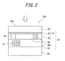
- FIG. 2 is a schematically cross-sectional view of a backside illumination type solid imaging device using the wafer for backside illumination type solid imaging device shown FIG. 1(a) after processing thereof.
- the wafer 10 for backside illumination type solid imaging device is a wafer 10 used in a backside illumination type solid imaging device 100 having a plurality of pixels 70 inclusive of a photoelectric conversion device 50 and a charge transfer transistor 60 at its a front surface side 40a and a light receiving surface at its backside 20a as shown in FIG. 2 .
- the wafer 10 for backside illumination type solid imaging device is mainly characterized to be a SOI wafer 10 obtained by forming a given active layer 40 on a support substrate 20 made of C-containing n-type or p-type semiconductor material through an insulating layer 30 as shown in FIG. 1(a) .
- the C atoms are taken into positions between silicon lattices in the support substrate 20 to promote precipitation of an oxygen-containing substance in a heat treatment step for producing the solid imaging device, and thus the oxygen precipitates can serve as a gettering site.
- the wafer 10 is used for the backside illumination type solid imaging device 100, the occurrence of white defects and heavy metal pollution can be effectively suppressed as compared with the conventional imaging devices.
- the support substrate 20 of the invention is a substrate made of n-type or P-type semiconductor material, which is required to contain a given amount of C for developing the above effect.
- the semiconductor used in the support substrate 20 is not particularly limited as long as it satisfies the above properties. From a point that the substrate can be obtained relatively easily, there are used a substrate 20 made of silicon material containing an elementary atom of the Group 15 such as P, As, Sb or the like for n-type, and a substrate 20 made of silicon material containing an elementary atom of the Group 13 such as B, Ga or the like for p-type.
- the support substrate 20 is preferably used a n-type or p-type carbon-containing substrate in view of strengthening the gettering ability. Further, the support substrate 20 is preferable to have a specific resistance of 0.5 to 100 ⁇ cm.
- the C concentration of the support substrate 20 is preferable to be within a range of 1.0x10 16 to 1.0x10 17 atoms/cm 3 .
- the C concentration is less than 1.0x10 16 atoms/cm 3 , there is a fear that the gettering ability can not be developed sufficiently and the occurrence of white defects and heavy metal pollution can not be sufficiently suppressed, while when it exceeds 1.0x10 17 atoms/cm 3 , the size of the oxygen precipitates is less than 50 nm and hence strain energy capable of gettering heavy metal can not be retained.
- the support substrate 20 can be processed until the thickness becomes not more than 20 ⁇ m.
- the thickness of the support substrate in the conventional wafer used for the backside illumination type solid imaging devices is 40 to 150 mm, whilst in this invention, the thickness may be made to not more than 20 ⁇ m because the thickened SIO structure is used.
- an insulating layer 30 is formed on the support substrate 20.
- the formation of the insulating layer 30 brings about the electric insulation between the support substrate 20 and the active layer 40, enabling smaller parasitic capacitance and speedup of the device.
- a kind of the insulating layer 30 is not particularly limited as long as it is an insulating film, but is preferable to be a silicon oxide film (SiO 2 ) from a point that it can be obtained relatively easily.
- the method for forming the insulating layer 30 will be concretely described later, since it is bonded to either the support substrate 20 or the active layer 40 (the support substrate 20 in the case of FIG. 1(a) ) at a state that the periphery thereof is oxidized as a whole, as shown in FIG. 1(a) , a residual oxide film 31 remains on the insulating layer 30 at a bonding interface of the wafer 10 for backside illumination type solid imaging device according to the invention but also around the support substrate 20.
- the residual oxide film 31 is already removed.
- the active layer 40 according to the invention is a layer formed on the insulating layer 30.
- it is a device layer arranged with the photoelectric conversion device 50 and the charge transfer transistor 60 as shown in FIG. 2 .
- it is preferably formed by bonding a wafer for active layer to a wafer for support substrate from a viewpoint that SOI being less in the defects and having the active layer 40 usable for an imaging device can be obtained simply. The detail of the production method will be described later.
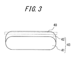
- FIG. 3 is schematically shown a cross-section of an epitaxial wafer as a wafer for active layer according to the invention.
- the active layer 40 is preferable to be an epitaxial layer 42 of Si formed on a substrate 41 for active layer made of C-containing n-type or p-type semiconductor material as shown in FIG. 3 .
- the epitaxial layer 42 formed on the substrate 41 for active layer made of C-containing n-type or p-type semiconductor material can provide the active layer 40 being less in the defects and having a high quality owing to the gettering effect of the C-containing substrate 41 for active layer. Therefore, when the active layer 40 is formed on the insulating layer 30, the effect of suppressing the occurrence of white defects and heavy metal pollution can be further improved in the solid imaging device 100 according to the invention.
- the C concentration in the substrate for active layer is preferable to be within a range of 1.0x10 16 to 1.0x10 17 atoms/cm 3 .
- the C concentration is less than 1.0x10 16 atoms/cm 3 likewise the case of the support substrate 20, there is a fear that the gettering ability can not be sufficiently developed and hence the white defects and heavy metal pollution generated in the active layer 40 can not be sufficiently suppressed, while when it exceeds 1.0x10 17 atoms/cm 3 , the size of the oxygen precipitates becomes minimal and it is difficult to retain strain energy required for the gettering and hence there is a fear that the gettering ability lowers.
- C atoms contained in the support substrate 20 are existent as a high carbon concentration region 21 just beneath an interface with the insulating layer 30 as shown in FIG. 1(b) .
- the high carbon concentration region 21 means a region having locally a large C content wherein the C concentration in the support substrate 20 is within a range of 1.0x10 16 to 1.0x10 17 atoms/cm 3 . Since the high carbon concentration region 21 serves as a gettering sink effectively, the effect of suppressing the occurrence of white defects and heavy metal pollution can be further improved.
- the backside illumination type solid imaging device 100 can be prepared when an embedded electrode (not shown) for transferring image data is connected to the pixels 70 including the wafer 10 for backside illumination type solid imaging device 10 of the invention.
- an embedded wiring 61 is disposed in the charge transfer transistor 60 and further a substrate 80 is arranged as a base for the pixels 70.
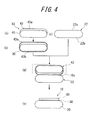
- FIG. 4 is a flow chart for explaining the method for producing the wafer for backside illumination type solid imaging device according to the invention.
- the wafer 10 for backside illumination type solid imaging device is characterized by forming an insulating layer 30 having a thickness of about 0.1 to 100 nm on a surface of a wafer 43 for active layer 43 ( FIG. 4(a) ), which is an epitaxial wafer obtained by forming an epitaxial film of Si on a substrate for active layer made of n-type or p-type semiconductor material preferably having a C concentration of 1.0x10 16 to 1.0x10 17 atoms/cm 3 , through a treatment such as thermal oxidation or the like ( FIG.
- FIG. 4(c) bonding a wafer 22 for support substrate made of n-type or p-type semiconductor material containing C (preferably C concentration: 1.0 ⁇ 10 16 to 1.0 ⁇ 10 17 atoms/cm 3 ) to the wafer 43 for active layer 43 through the insulating layer 30 ( FIG. 4(d) ), and then thinning the wafer 43 for active layer 43 to form SOI wafer 10 ( FIG. 4(e) ).
- C preferably C concentration: 1.0 ⁇ 10 16 to 1.0 ⁇ 10 17 atoms/cm 3
- the C atoms in the support substrate 20 are taken into positions between silicon lattices in the support substrate 20 to promote the precipitation of oxygen-containing substance in a heat treatment step for the production of the solid imaging device, and thus the oxygen precipitates can serve as a gettering site.
- the wafer 10 is used for the backside illumination type solid imaging device 100, the occurrence of white defects and heavy metal pollution can be effectively suppressed as compared with the conventional imaging devices.
- the insulating layer 30 is formed by subjecting the wafer 43 for active layer to a thermal oxidation treatment, which is merely one embodiment of the invention. In fact, it is also possible to form the insulating layer 30 on the wafer 22 for support substrate and then bond to the wafer 43.
- a method of including a given amount of C into the wafer 22 for support substrate and the wafer 43 for active layer there are a method of doping a silicon substrate with C atoms, a method of implanting ions and so on, whereby it is made possible to include the C atoms into the wafer 22 for support substrate.
- O atoms can be included into the wafer 22 for support substrate and the wafer 43 for active layer.
- the inclusion of the O atoms can effectively suppress the diffusion of the C atoms included for the gettering effect into the active layer.
- each of the wafer 43 for support substrate and the wafer 22 for active layer is subjected to a heat treatment at 600-800°C before the bonding of the wafers 22 and 43. Since the precipitation of oxygen is promoted by this heat treatment, it is possible to form high-density oxygen precipitates.
- the bonding is conducted after a given organic substance is adsorbed on bonding surfaces 22a, 43a of the wafer 22 for support substrate and/or the wafer 43 for active layer 43.
- the bonding is conducted after the adsorption of the organic substance on the bonding surface(s) ( FIG. 4 (d) )
- the organic substance forms the high carbon concentration region 21 at the bonding interface 10a by the heat treatment in the bonding, and hence the further improvement of the gettering ability is expected in the wafer 10 according to the invention.
- organic substance is preferable an organic carbon compound such as N-methyl pyrrolidone, polyvinyl pyrrolidone or the like. By using such an organic substance can be simply formed the high carbon concentration region 21.
- a polysilicon film (not shown) is formed on surfaces 22b, 43b opposite to the bonding surfaces 22a, 43a of the wafer 22 for support substrate and the wafer 43 for active layer, respectively.
- the resulting polysilicon film serves as a gettering sink, which is expected to further improve the gettering effect.
- a wafer for backside illumination type solid imaging device is prepared as a sample and its performances are evaluated as described below.
- an epitaxial wafer obtained by forming an epitaxial film of Si on a substrate 41 for active layer made of C-containing n-type silicon (C concentration: 1.0 ⁇ 10 16 atoms/cm 3 , specific resistance: 10 ⁇ cm) through a CVD method as a wafer 43 for active layer ( FIG. 4(a) ), and then an insulating layer 30 having a thickness of 0.1 ⁇ m is formed on the surface thereof by a thermal oxidation treatment ( FIG. 4(b) ).
- a wafer 22 for support substrate of n-type silicon made of C-containing n-type semiconductor material (C concentration: 1.0 ⁇ 10 16 atoms/cm 3 , specific resistance: 10 ⁇ cm) ( FIG. 4(c) ) is bonded to the wafer 43 for active layer through the insulating layer 30 ( FIG. 4(d) ), and then the wafer 43 for active layer is thinned by polishing and chemical etching to prepare a sample of a wafer 10 for backside illumination type solid imaging device as a SOI wafer having the given support substrate 20, insulating layer 30 and active layer 40 ( FIG. 4 (e) ).
- a sample of a wafer 10 for backside illumination type solid imaging device is prepared in the same steps as in Example 1 ( FIGS. 4(a) to (e) ) except that an organic substance, N-methyl pyrrolidone is adsorbed on a bonding surface 22a of the wafer 22 for support substrate 22 before the step of bonding the wafer 22 for support substrate to the wafer 43 for active layer ( FIG. 4(d) ) and then the bonding and heat treatment are conducted to form a high carbon concentration region 21 on a bonding interface 10a.
- an organic substance, N-methyl pyrrolidone is adsorbed on a bonding surface 22a of the wafer 22 for support substrate 22 before the step of bonding the wafer 22 for support substrate to the wafer 43 for active layer ( FIG. 4(d) ) and then the bonding and heat treatment are conducted to form a high carbon concentration region 21 on a bonding interface 10a.
- a sample of a wafer 10 for backside illumination type solid imaging device is prepared in the same steps as in Example 1 ( FIGS. 4(a) to (e) ) except that a polysilicon film (not shown) is formed on surfaces 22b, 43b opposite to the bonding surfaces 22a, 43a of the wafer 22 for support substrate and the wafer 43 for active layer, respectively.
- an epitaxial wafer obtained by forming an epitaxial film of Si on a substrate 41 for active layer made of C-containing p-type silicon (C concentration: 1.0 ⁇ 10 15 atoms/cm 3 , specific resistance: 10 m ⁇ cm) through a CVD method as a wafer 43 for active layer ( FIG. 4(a) ), and then an insulating layer 30 having a thickness of 0.1 ⁇ m is formed on the surface thereof by a thermal oxidation treatment ( FIG. 4(b) ). Thereafter, a wafer 22 for support substrate made of C-containing p-type semiconductor material (C concentration: 1.0 ⁇ 10 15 atoms/cm 3 , specific resistance: 10 m ⁇ cm) ( FIG.
- Samples of a wafer 10 for backside illumination type solid imaging device are prepared by the same steps as in Example 4 ( FIGS. 4(a) to (e) ) except that the wafer 22 for support substrate and the wafer 43 for active layer are 43 have C concentration values as shown in Table 1, respectively.
- a sample of a wafer 10 for backside illumination type solid imaging device is prepared in the same steps as in Example 1 ( FIGS. 4(a) to (e) ) except that the wafer 22 for support substrate and the wafer 43 for active layer are 43 have C concentration values as shown in Table I, respectively, and an organic substance, N-methyl pyrrolidone is adsorbed on a bonding surface 22a of the wafer 22 for support substrate 22 before the step of bonding the wafer 22 for support substrate to the wafer 43 for active layer ( FIG. 4(d) ) and then the bonding and heat treatment are conducted to form a high carbon concentration region 21 on a bonding interface 10a.
- a sample of a wafer 10 for backside illumination type solid imaging device is prepared in the same steps as in Example 4 ( FIGS. 4(a) to (e) ) except that the wafer 22 for support substrate and the wafer 43 for active layer are 43 have C concentration values as shown in Table 1, respectively, and a polysilicon film (not shown) is formed on surfaces 22b, 43b opposite to the bonding surfaces 22a, 43a of the wafer 22 for support substrate and the wafer 43 for active layer, respectively.
- a sample of a wafer 10 for backside illumination type solid imaging device is prepared as a usual bonded SOI formed by bonding a wafer for support substrate made of Si (not including C) to a wafer for active layer made of Si through an oxide film and then removing a part of the wafer for active layer.
- a backside illumination type solid imaging device is prepared by using each sample prepared in the above examples and comparative example, and thereafter the dark leakage current of a photodiode in the backside illumination type solid imaging device is measured and converted to pixel data (number data of white defects) with a semiconductor parameter analyzing apparatus, whereby the number of white defects per unit area (1 cm 2 ) is counted to evaluate the suppression on the occurrence of white defects.
- the evaluation standard is shown below, and the measured results and evaluation results are shown in Table 1.
- the defect density (number/cm 2 ) on the surface of each obtained sample is measured by soiling the sample surface with nickel (1.0x10 12 atoms/cm 2 ) by a spin coat soiling method and thereafter subjecting to a heat treatment at 900°C for 1 hour and then selectively etching the surface of the sample.
- the evaluation standard is shown below, and the measured results and evaluation results are shown in Table 1.
- Example 1 C content (atoms/cm 3 ) Presence or absence of high carbon concentration region Presence or absence of polysilicon film Evaluation results Support substrate Active layer White defects Heavy metal pollution Evaluation Evaluation
- Example 1 1.00E+16 1.00E+16 - - ⁇ ⁇
- Example 2 5.00E+16 5.00E+16 Presence - ⁇ ⁇
- Example 3 7.00E+16 7.00E+16 - Presence ⁇ ⁇
- Example 4 1.00E+15 1.00E+15 - - ⁇ ⁇
- Example 5 5.00E+15 5.00E+15 Presence - ⁇ ⁇
- Example 6 5.00E+16 5.00E+16 - Presence ⁇ ⁇
- Example 7 7.00E+16 7.00E+16 - - ⁇ ⁇
- Example 8 7.00E+16 7.00E+16 - - ⁇ ⁇
- Example 9 5.00E+15 7.00E+16 - - ⁇ ⁇ Comparative Example - - - -
- Examples 1 to 10 can suppress the occurrence of white defects and heavy metal pollution as compared with the comparative example. Furthermore, it is found that Examples 2, 3 and 5-10 are high in the gettering ability and further higher in the effect of suppressing the occurrence of white defect and heavy metal pollution as compared to Examples 1 and 4.
- the invention it is possible to provide a wafer for backside illumination type solid imaging device capable of suppressing the occurrence of white defects and heavy metal pollution effectively, a production method thereof and a backside illumination type solid imaging device.
Landscapes
- Solid State Image Pick-Up Elements (AREA)
Abstract
Description
- This invention relates to a silicon substrate, a production method thereof and a device using the substrate, and more particularly to a wafer for backside illumination type solid imaging device, which is used in mobile phones, digital video cameras and the like and is capable of suppressing white defects effectively, a production method thereof and a backside illumination type solid imaging device.
- Recently, a high-performance solid imaging device using a semiconductor is mounted onto a mobile phone, a digital video camera or the like, and hence the performances such as number of pixcels and the like are dramatically improved. As the performance to be expected in the usual solid imaging device are high-quality pixels and ability of taking moving images, and further miniaturization is required. In order to take moving images, it is required to combine a high-speed computing device with a memory device, and hence a CMOS image sensor allowing System on Chip (SoC) easily is used and the downsizing of the CMOS image sensor is developed.
- With the downsizing of the CMOS image sensor, however, there is caused a problem that an aperture ratio of a photo diode as a photoelectric conversion device is inevitably reduced to lower a quantum efficiency of the photoelectric conversion device, which makes it difficult to improve S/N ratio of imaging data. Therefore, it is attempted to conduct a method for increasing incident light quantity by inserting an inner lens into a front side of the photoelectric conversion device, or the like. However, the remarkable improvement of S/N ratio can not been realized.
- In order to increase the incident light quantity to improve S/N ratio of the image data, therefore, it is attempted to feed the incident light from a backside of the photoelectric conversion device. The greatest merit of the light incidence from the backside of the device lies in a point that restriction due to reflection or diffraction on the surface of the device or the light receiving area of the device is eliminated as compared with the light incidence from the front side. On the other hand, when the light is entered from the backside, the absorption of the light through a silicon wafer as a substrate of the photoelectric conversion device must be suppressed, and hence the thickness of the solid imaging device as a whole is required to be less than 50 µm. As a result, the working and handling of the solid imaging device become difficult, causing a problem of extremely low productivity.
- For the purpose of resolving the above technical problems, there are mentioned solid imaging devices as disclosed, for example, in
JP-A-2007-13089 JP-A-2007-59755 - When using the production method of the solid imaging device in
JP-A-2007-13089 - On the other hand, when using the production method of the solid imaging device in
JP-A-2007-59755 - In the solid imaging devices of
JP-A-2007-13089 JP-A-2007-59755 - It is, therefore, an object of the invention to provide a wafer for backside illumination type solid imaging device capable of effectively suppressing the occurrence of white defects and heavy metal pollution, and a production method thereof and a backside illumination type solid imaging device.
- In order to achieve the above object, the summary and construction of the invention are as follows.
- (1) A wafer for backside illumination type solid imaging device having a plurality of pixels inclusive of a photoelectric conversion device and a charge transfer transistor at its front surface side and a light receiving surface at its back surface side, characterized in that said wafer is a SOI wafer obtained by forming a given active layer on a support substrate made of C-containing n-type or p-type semiconductor material through an insulating layer.
- (2) A wafer for backside illumination type solid imaging device according to the item (1), wherein the active layer is an epitaxial layer of Si formed on a substrate for active layer made of C-containing n-type or p-type semiconductor material.
- (3) A wafer for backside illumination type solid imaging device according to the item (2), wherein the C concentration in the support substrate and the substrate for active layer is within a range of 1.0x10¹⁶ to 1.0x10¹⁷ atoms/cm3.
- (4) A wafer for backside illumination type solid imaging device according to the item (1), (2) or (3), wherein C atoms contained in the support substrate are existent as a high carbon concentration region having a C concentration of 1.0x10¹⁶ to 1.0x10¹⁷ atoms/cm3 just beneath an interface with the insulating layer.
- (5) A wafer for backside illumination type solid imaging device according to any one of the items (1) to (4), wherein the support substrate made of n-type semiconductor material further contains P, As or Sb.
- (6) A wafer for backside illumination type solid imaging device according to any one of the items (1) to (4), wherein the support substrate made of p-type semiconductor material further contains B or Ga.
- (7) A backside illumination type solid imaging device comprising an embedded electrode for transferring image data connected to pixels of a wafer for backside illumination type solid imaging device as described in any one of the items (1) to (6).
- (8) A method for producing a wafer for backside illumination type solid imaging device having a plurality of pixels inclusive of a photoelectric conversion device and a charge transfer transistor at its front surface side and a light receiving surface at its back surface side, characterized in that a silicon substrate is formed by bonding a wafer for support substrate made of C-containing n-type or p-type semiconductor material to a given wafer for active layer through an insulating film and then thinning the wafer for active layer.
- (9) The method according to the item (8), wherein the wafer for active layer is an epitaxial wafer obtained by forming an epitaxial film of Si on a substrate for active layer made of C-containing n-type or p-type semiconductor material.
- (10) The method according to the item (9), wherein a C concentration in the support substrate and the substrate for active layer is within a range of 1.0x10¹⁶ to 1.0x10¹⁷ atoms/cm3.
- (11) The method according to the item (8), (9) or (10), wherein each of the wafer for support substrate and the wafer for active layer is subjected to a heat treatment at 600 to 800°C before bonding thereof.
- (12) The method according to any ane of the items (8) to (11), wherein the bonding is conducted after a given organic substance is adsorbed on a bonding surface of the wafer for support substrate and/or the wafer for active layer.
- (13) The method according to the item (12), wherein the organic substance is an organic carbon compound.
- (14) The method according to any one of the items (8) to (13), wherein a polysilicon film is formed on each surface opposite to bonding surfaces of the wafer for support substrate and the wafer for active layer.
- According to the invention, it is possible to provide a wafer for backside illumination type solid imaging device capable of effectively suppressing occurrence of white defects and heavy metal pollution, a production method thereof and a backside illumination type solid imaging device.
- The invention will be described with reference to the accompanying drawings, wherein:
-
FIG. 1 is a schematically cross-sectional view of a wafer for backside illumination type solid imaging device according to the invention; -
FIG. 2 is a schematically cross-sectional view of a backside illumination type solid imaging device of the invention; -
FIG. 3 is a schematically cross-sectional view of a wafer for active layer used in a wafer for backside illumination type solid imaging device according to the invention; and -
FIG. 4 is a schematic flow chart of steps for producing a wafer for backside illumination type solid imaging device according to the invention, wherein (a) is a wafer for active layer, (b) is a wafer for active layer provided with an insulating film formed thereon, (c) is a wafer for support substrate, (d) is a state of bonding a wafer for active layer to a wafer for support substrate, and (e) is a wafer for backside illumination type solid imaging device according to the invention. - Each of
FIGS. 1(a) and 1(b) is a schematically cross-sectional view of a wafer for backside illumination type solid imaging device according to the invention. Further,FIG. 2 is a schematically cross-sectional view of a backside illumination type solid imaging device using the wafer for backside illumination type solid imaging device shownFIG. 1(a) after processing thereof. - The
wafer 10 for backside illumination type solid imaging device according to the invention is awafer 10 used in a backside illumination typesolid imaging device 100 having a plurality ofpixels 70 inclusive of aphotoelectric conversion device 50 and acharge transfer transistor 60 at its afront surface side 40a and a light receiving surface at itsbackside 20a as shown inFIG. 2 . - The
wafer 10 for backside illumination type solid imaging device according to the invention is mainly characterized to be aSOI wafer 10 obtained by forming a givenactive layer 40 on asupport substrate 20 made of C-containing n-type or p-type semiconductor material through aninsulating layer 30 as shown inFIG. 1(a) . By adopting such a structure, the C atoms are taken into positions between silicon lattices in thesupport substrate 20 to promote precipitation of an oxygen-containing substance in a heat treatment step for producing the solid imaging device, and thus the oxygen precipitates can serve as a gettering site. As a result, when thewafer 10 is used for the backside illumination typesolid imaging device 100, the occurrence of white defects and heavy metal pollution can be effectively suppressed as compared with the conventional imaging devices. - The components in the
wafer 10 for backside illumination type solid imaging device according to the invention will be described below. - The
support substrate 20 of the invention is a substrate made of n-type or P-type semiconductor material, which is required to contain a given amount of C for developing the above effect. The semiconductor used in thesupport substrate 20 is not particularly limited as long as it satisfies the above properties. From a point that the substrate can be obtained relatively easily, there are used asubstrate 20 made of silicon material containing an elementary atom of the Group 15 such as P, As, Sb or the like for n-type, and asubstrate 20 made of silicon material containing an elementary atom of the Group 13 such as B, Ga or the like for p-type. - Also, as the
support substrate 20 is preferably used a n-type or p-type carbon-containing substrate in view of strengthening the gettering ability. Further, thesupport substrate 20 is preferable to have a specific resistance of 0.5 to 100 Ω·cm. - Moreover, the C concentration of the
support substrate 20 is preferable to be within a range of 1.0x10¹⁶ to 1.0x10¹⁷ atoms/cm3. When the C concentration is less than 1.0x10¹⁶ atoms/cm3, there is a fear that the gettering ability can not be developed sufficiently and the occurrence of white defects and heavy metal pollution can not be sufficiently suppressed, while when it exceeds 1.0x10¹⁷ atoms/cm3, the size of the oxygen precipitates is less than 50 nm and hence strain energy capable of gettering heavy metal can not be retained. - Since the
wafer 10 of the invention is used in the backside illumination typesolid imaging device 100, when it is used as a device as shown inFIG. 2 , thesupport substrate 20 can be processed until the thickness becomes not more than 20 µm. The thickness of the support substrate in the conventional wafer used for the backside illumination type solid imaging devices is 40 to 150 mm, whilst in this invention, the thickness may be made to not more than 20 µm because the thickened SIO structure is used. - Since the
wafer 10 for backside illumination type solid imaging device according to the invention is SOI, aninsulating layer 30 is formed on thesupport substrate 20. The formation of the insulatinglayer 30 brings about the electric insulation between thesupport substrate 20 and theactive layer 40, enabling smaller parasitic capacitance and speedup of the device. A kind of the insulatinglayer 30 is not particularly limited as long as it is an insulating film, but is preferable to be a silicon oxide film (SiO2) from a point that it can be obtained relatively easily. - Although the method for forming the insulating
layer 30 will be concretely described later, since it is bonded to either thesupport substrate 20 or the active layer 40 (thesupport substrate 20 in the case ofFIG. 1(a) ) at a state that the periphery thereof is oxidized as a whole, as shown inFIG. 1(a) , aresidual oxide film 31 remains on the insulatinglayer 30 at a bonding interface of thewafer 10 for backside illumination type solid imaging device according to the invention but also around thesupport substrate 20. When thewafer 10 is used in theimaging device 100, since it is subjected to the processing, theresidual oxide film 31 is already removed. - The
active layer 40 according to the invention is a layer formed on the insulatinglayer 30. In the invention, it is a device layer arranged with thephotoelectric conversion device 50 and thecharge transfer transistor 60 as shown inFIG. 2 . Moreover, it is preferably formed by bonding a wafer for active layer to a wafer for support substrate from a viewpoint that SOI being less in the defects and having theactive layer 40 usable for an imaging device can be obtained simply. The detail of the production method will be described later. - In
FIG. 3 is schematically shown a cross-section of an epitaxial wafer as a wafer for active layer according to the invention. Theactive layer 40 is preferable to be anepitaxial layer 42 of Si formed on asubstrate 41 for active layer made of C-containing n-type or p-type semiconductor material as shown inFIG. 3 . Theepitaxial layer 42 formed on thesubstrate 41 for active layer made of C-containing n-type or p-type semiconductor material can provide theactive layer 40 being less in the defects and having a high quality owing to the gettering effect of the C-containingsubstrate 41 for active layer. Therefore, when theactive layer 40 is formed on the insulatinglayer 30, the effect of suppressing the occurrence of white defects and heavy metal pollution can be further improved in thesolid imaging device 100 according to the invention. - Furthermore, the C concentration in the substrate for active layer is preferable to be within a range of 1.0x10¹⁶ to 1.0x10¹⁷ atoms/cm3. When the C concentration is less than 1.0x10¹⁶ atoms/cm3 likewise the case of the
support substrate 20, there is a fear that the gettering ability can not be sufficiently developed and hence the white defects and heavy metal pollution generated in theactive layer 40 can not be sufficiently suppressed, while when it exceeds 1.0x10¹⁷ atoms/cm3, the size of the oxygen precipitates becomes minimal and it is difficult to retain strain energy required for the gettering and hence there is a fear that the gettering ability lowers. - Moreover, it is preferable that C atoms contained in the
support substrate 20 are existent as a highcarbon concentration region 21 just beneath an interface with the insulatinglayer 30 as shown inFIG. 1(b) . The highcarbon concentration region 21 means a region having locally a large C content wherein the C concentration in thesupport substrate 20 is within a range of 1.0x10¹⁶ to 1.0x10¹⁷ atoms/cm3. Since the highcarbon concentration region 21 serves as a gettering sink effectively, the effect of suppressing the occurrence of white defects and heavy metal pollution can be further improved. - Moreover, as shown in
FIG. 2 , the backside illumination typesolid imaging device 100 can be prepared when an embedded electrode (not shown) for transferring image data is connected to thepixels 70 including thewafer 10 for backside illumination typesolid imaging device 10 of the invention. By the gettering effect of thewafer 10 for backside illumination typesolid imaging device 10 according to the invention, it is made possible to provide the backside illumination typesolid imaging device 100 being excellent in the ability of suppressing the occurrence of white defects and heavy metal pollution as compared with the conventional backside illumination type solid imaging device. InFIG. 2 , an embeddedwiring 61 is disposed in thecharge transfer transistor 60 and further asubstrate 80 is arranged as a base for thepixels 70. - Subsequently, the method for producing the wafer for backside illumination type solid imaging device according to the invention will be described with reference to the accompanying drawings.
FIG. 4 is a flow chart for explaining the method for producing the wafer for backside illumination type solid imaging device according to the invention. - As shown in
FIG. 4 , thewafer 10 for backside illumination type solid imaging device according to the invention is characterized by forming an insulatinglayer 30 having a thickness of about 0.1 to 100 nm on a surface of awafer 43 for active layer 43 (FIG. 4(a) ), which is an epitaxial wafer obtained by forming an epitaxial film of Si on a substrate for active layer made of n-type or p-type semiconductor material preferably having a C concentration of 1.0x10¹⁶ to 1.0x10¹⁷ atoms/cm3, through a treatment such as thermal oxidation or the like (FIG. 4 (b) ), and thereafter bonding awafer 22 for support substrate made of n-type or p-type semiconductor material containing C (preferably C concentration: 1.0×10¹⁶ to 1.0×10¹⁷ atoms/cm3) (FIG. 4(c) ) to thewafer 43 foractive layer 43 through the insulating layer 30 (FIG. 4(d) ), and then thinning thewafer 43 foractive layer 43 to form SOI wafer 10 (FIG. 4(e) ). - When the
wafer 10 for backside illumination type solid imaging device is formed by the above method, the C atoms in thesupport substrate 20 are taken into positions between silicon lattices in thesupport substrate 20 to promote the precipitation of oxygen-containing substance in a heat treatment step for the production of the solid imaging device, and thus the oxygen precipitates can serve as a gettering site. As a result, when thewafer 10 is used for the backside illumination typesolid imaging device 100, the occurrence of white defects and heavy metal pollution can be effectively suppressed as compared with the conventional imaging devices. - In
FIG. 4 , the insulatinglayer 30 is formed by subjecting thewafer 43 for active layer to a thermal oxidation treatment, which is merely one embodiment of the invention. In fact, it is also possible to form the insulatinglayer 30 on thewafer 22 for support substrate and then bond to thewafer 43. - As a method of including a given amount of C into the
wafer 22 for support substrate and thewafer 43 for active layer, there are a method of doping a silicon substrate with C atoms, a method of implanting ions and so on, whereby it is made possible to include the C atoms into thewafer 22 for support substrate. - Also, O atoms can be included into the
wafer 22 for support substrate and thewafer 43 for active layer. The inclusion of the O atoms can effectively suppress the diffusion of the C atoms included for the gettering effect into the active layer. - Furthermore, it is preferable that each of the
wafer 43 for support substrate and thewafer 22 for active layer is subjected to a heat treatment at 600-800°C before the bonding of thewafers - Moreover, it is preferable that the bonding is conducted after a given organic substance is adsorbed on
bonding surfaces wafer 22 for support substrate and/or thewafer 43 foractive layer 43. When the bonding is conducted after the adsorption of the organic substance on the bonding surface(s) (FIG. 4 (d) ), the organic substance forms the highcarbon concentration region 21 at thebonding interface 10a by the heat treatment in the bonding, and hence the further improvement of the gettering ability is expected in thewafer 10 according to the invention. - As the organic substance is preferable an organic carbon compound such as N-methyl pyrrolidone, polyvinyl pyrrolidone or the like. By using such an organic substance can be simply formed the high
carbon concentration region 21. - In the production method of the invention, it is preferable that a polysilicon film (not shown) is formed on
surfaces bonding surfaces wafer 22 for support substrate and thewafer 43 for active layer, respectively. The resulting polysilicon film serves as a gettering sink, which is expected to further improve the gettering effect. - Although the above is described with respect to only one embodiment of the invention, various modifications may be made without departing from the scope of the appended claims.
- A wafer for backside illumination type solid imaging device according to the invention is prepared as a sample and its performances are evaluated as described below.
- As shown in
FIG. 4 , there is provided an epitaxial wafer obtained by forming an epitaxial film of Si on asubstrate 41 for active layer made of C-containing n-type silicon (C concentration: 1.0×10¹⁶ atoms/cm3, specific resistance: 10 Ω·cm) through a CVD method as awafer 43 for active layer (FIG. 4(a) ), and then an insulatinglayer 30 having a thickness of 0.1 µm is formed on the surface thereof by a thermal oxidation treatment (FIG. 4(b) ). Thereafter, awafer 22 for support substrate of n-type silicon made of C-containing n-type semiconductor material (C concentration: 1.0×10¹⁶ atoms/cm3, specific resistance: 10 Ω·cm) (FIG. 4(c) ) is bonded to thewafer 43 for active layer through the insulating layer 30 (FIG. 4(d) ), and then thewafer 43 for active layer is thinned by polishing and chemical etching to prepare a sample of awafer 10 for backside illumination type solid imaging device as a SOI wafer having the givensupport substrate 20, insulatinglayer 30 and active layer 40 (FIG. 4 (e) ). - A sample of a
wafer 10 for backside illumination type solid imaging device is prepared in the same steps as in Example 1 (FIGS. 4(a) to (e) ) except that an organic substance, N-methyl pyrrolidone is adsorbed on abonding surface 22a of thewafer 22 forsupport substrate 22 before the step of bonding thewafer 22 for support substrate to thewafer 43 for active layer (FIG. 4(d) ) and then the bonding and heat treatment are conducted to form a highcarbon concentration region 21 on abonding interface 10a. - A sample of a
wafer 10 for backside illumination type solid imaging device is prepared in the same steps as in Example 1 (FIGS. 4(a) to (e) ) except that a polysilicon film (not shown) is formed onsurfaces bonding surfaces wafer 22 for support substrate and thewafer 43 for active layer, respectively. - As shown in
FIG. 4 , there is provided an epitaxial wafer obtained by forming an epitaxial film of Si on asubstrate 41 for active layer made of C-containing p-type silicon (C concentration: 1.0×10¹⁵ atoms/cm3, specific resistance: 10 mΩ·cm) through a CVD method as awafer 43 for active layer (FIG. 4(a) ), and then an insulatinglayer 30 having a thickness of 0.1 µm is formed on the surface thereof by a thermal oxidation treatment (FIG. 4(b) ). Thereafter, awafer 22 for support substrate made of C-containing p-type semiconductor material (C concentration: 1.0×10¹⁵ atoms/cm3, specific resistance: 10 mΩ·cm) (FIG. 4(c) ) is bonded to thewafer 43 for active layer through the insulating layer 30 (FIG. 4(d) ), and then thewafer 43 for active layer is thinned by polishing and chemical etching to prepare a sample of awafer 10 for backside illumination type solid imaging device as a SOI wafer having the givensupport substrate 20, insulatinglayer 30 and active layer 40 (FIG. 4 (e) ). - Samples of a
wafer 10 for backside illumination type solid imaging device are prepared by the same steps as in Example 4 (FIGS. 4(a) to (e) ) except that thewafer 22 for support substrate and thewafer 43 for active layer are 43 have C concentration values as shown in Table 1, respectively. - A sample of a
wafer 10 for backside illumination type solid imaging device is prepared in the same steps as in Example 1 (FIGS. 4(a) to (e) ) except that thewafer 22 for support substrate and thewafer 43 for active layer are 43 have C concentration values as shown in Table I, respectively, and an organic substance, N-methyl pyrrolidone is adsorbed on abonding surface 22a of thewafer 22 forsupport substrate 22 before the step of bonding thewafer 22 for support substrate to thewafer 43 for active layer (FIG. 4(d) ) and then the bonding and heat treatment are conducted to form a highcarbon concentration region 21 on abonding interface 10a. - A sample of a
wafer 10 for backside illumination type solid imaging device is prepared in the same steps as in Example 4 (FIGS. 4(a) to (e) ) except that thewafer 22 for support substrate and thewafer 43 for active layer are 43 have C concentration values as shown in Table 1, respectively, and a polysilicon film (not shown) is formed onsurfaces bonding surfaces wafer 22 for support substrate and thewafer 43 for active layer, respectively. - A sample of a
wafer 10 for backside illumination type solid imaging device is prepared as a usual bonded SOI formed by bonding a wafer for support substrate made of Si (not including C) to a wafer for active layer made of Si through an oxide film and then removing a part of the wafer for active layer. - Each sample prepared in the above examples and comparative example is evaluated by the following evaluation methods.
- A backside illumination type solid imaging device is prepared by using each sample prepared in the above examples and comparative example, and thereafter the dark leakage current of a photodiode in the backside illumination type solid imaging device is measured and converted to pixel data (number data of white defects) with a semiconductor parameter analyzing apparatus, whereby the number of white defects per unit area (1 cm2) is counted to evaluate the suppression on the occurrence of white defects. The evaluation standard is shown below, and the measured results and evaluation results are shown in Table 1.
- ⊚ : not more than 5
- ○ : more than 5 but not more than 50
- × : more than 50
- The defect density (number/cm2) on the surface of each obtained sample is measured by soiling the sample surface with nickel (1.0x10¹² atoms/cm2) by a spin coat soiling method and thereafter subjecting to a heat treatment at 900°C for 1 hour and then selectively etching the surface of the sample. The evaluation standard is shown below, and the measured results and evaluation results are shown in Table 1.
- ⊚ : not more than 5
- ○ : more than 5 but not more than 50
- × : more than 50
-
Table 1 C content (atoms/cm3) Presence or absence of high carbon concentration region Presence or absence of polysilicon film Evaluation results Support substrate Active layer White defects Heavy metal pollution Evaluation Evaluation Example 1 1.00E+16 1.00E+16 - - ○ ○ Example 2 5.00E+16 5.00E+16 Presence - ⊚ ⊚ Example 3 7.00E+16 7.00E+16 - Presence ⊚ ⊚ Example 4 1.00E+15 1.00E+15 - - ○ ○ Example 5 5.00E+15 5.00E+15 Presence - ⊚ ⊚ Example 6 5.00E+16 5.00E+16 - Presence ⊚ ⊚ Example 7 7.00E+16 7.00E+16 - - ⊚ ⊚ Example 8 7.00E+16 7.00E+16 - - ⊚ ⊚ Example 9 5.00E+15 7.00E+16 - - ⊚ ⊚ Example 10 7.00E+16 5.00E+15 - - ⊚ ⊚ Comparative Example - - - - × × - As seen from the results of Table 1, Examples 1 to 10 can suppress the occurrence of white defects and heavy metal pollution as compared with the comparative example. Furthermore, it is found that Examples 2, 3 and 5-10 are high in the gettering ability and further higher in the effect of suppressing the occurrence of white defect and heavy metal pollution as compared to Examples 1 and 4.
- According to the invention, it is possible to provide a wafer for backside illumination type solid imaging device capable of suppressing the occurrence of white defects and heavy metal pollution effectively, a production method thereof and a backside illumination type solid imaging device.
Claims (14)
- A wafer for backside illumination type solid imaging device having a plurality of pixels inclusive of a photoelectric conversion device and a charge transfer transistor at its front surface side and a light receiving surface at its a back surface side, characterized in that said wafer is a SOI wafer obtained by forming a given active layer on a support substrate made of C-containing n-type or p-type semiconductor material through an insulating layer.
- A wafer for backside illumination type solid imaging device according to claim 1, wherein the active layer is an epitaxial layer of Si formed on a substrate for active layer made of C-containing n-type or p-type semiconductor material.
- A wafer for backside illumination type solid imaging device according to claim 2, wherein the C concentration in the support substrate and the substrate for active layer is within a range of 1.0x10¹⁶ to 1.0x10¹⁷ atoms/cm3.
- A wafer for backside illumination type solid imaging device according to claim 1, 2 or 3, wherein C atoms contained in the support substrate are existent as a high carbon concentration region having a C concentration of 1.0x10¹⁶ to 1.0x10¹⁷ atoms/cm3 just beneath an interface with the insulating layer.
- A wafer for backside illumination type solid imaging device according to any one of claims 1 to 4, wherein the support substrate made of n-type semiconductor material further contains P, As or Sb.
- A wafer for backside illumination type solid imaging device according to any one of claims 1 to 4, wherein the support substrate made of p-type semiconductor material further contains B or Ga.
- A backside illumination type solid imaging device comprising an embedded electrode for transferring image data connected to pixels of a wafer for backside illumination type solid imaging device as claimed in any one of claims 1 to 6.
- A method for producing a wafer for backside illumination type solid imaging device having a plurality of pixels inclusive of a photoelectric conversion device and a charge transfer transistor at its front surface side and a light receiving surface at its back surface side, characterized in that a silicon substrate is formed by bonding a wafer for support substrate made of C-containing n-type or p-type semiconductor material to a given wafer for active layer through an insulating film and then thinning the wafer for active layer.
- The method according to claim 8, wherein the wafer for active layer is an epitaxial wafer obtained by forming an epitaxial film of Si on a substrate for active layer made of C-containing n-type or p-type semiconductor material.
- The method according to claim 9, wherein a C concentration in the support substrate and the substrate for active layer is within a range of 1.0x10¹⁶ to 1.0x10¹⁷ atoms/cm3.
- The method according to claim 8, 9 or 10, wherein each of the wafer for support substrate and the wafer for active layer is subjected to a heat treatment at 600 to 800°C before bonding thereof.
- The method according to any one of claims 8 to 11, wherein the bonding is conducted after a given organic substance is adsorbed on a bonding surface of the wafer for support substrate and/or the wafer for active layer.
- The method according to claim 12, wherein the organic substance is an organic carbon compound.
- The method according to any one of claims 8 to 13, wherein a polysilicon film is formed on each surface opposite to the bonding surfaces of the wafer for support substrate and the wafer for active layer.
Applications Claiming Priority (2)
| Application Number | Priority Date | Filing Date | Title |
|---|---|---|---|
| JP2008077756A JP2009231706A (en) | 2008-03-25 | 2008-03-25 | Wafer for backside illuminated solid-state imaging device, method of manufacturing the same, and backside illuminated solid-state imaging device |
| JP2008131699A JP2009283533A (en) | 2008-05-20 | 2008-05-20 | Wafer for back-illuminated solid-state image sensor, method of manufacturing the same, and back-illuminated solid-state image sensor |
Publications (2)
| Publication Number | Publication Date |
|---|---|
| EP2105954A1 true EP2105954A1 (en) | 2009-09-30 |
| EP2105954B1 EP2105954B1 (en) | 2012-03-21 |
Family
ID=40823181
Family Applications (1)
| Application Number | Title | Priority Date | Filing Date |
|---|---|---|---|
| EP09155898A Not-in-force EP2105954B1 (en) | 2008-03-25 | 2009-03-23 | Method of manufacturing a backside illumination solid imaging device |
Country Status (4)
| Country | Link |
|---|---|
| US (1) | US20090242939A1 (en) |
| EP (1) | EP2105954B1 (en) |
| KR (2) | KR20090102704A (en) |
| TW (1) | TW200952163A (en) |
Cited By (1)
| Publication number | Priority date | Publication date | Assignee | Title |
|---|---|---|---|---|
| WO2011067916A1 (en) * | 2009-12-04 | 2011-06-09 | Canon Kabushiki Kaisha | Solid-state image pickup device and method for manufacturing the same |
Families Citing this family (2)
| Publication number | Priority date | Publication date | Assignee | Title |
|---|---|---|---|---|
| JP2009283533A (en) * | 2008-05-20 | 2009-12-03 | Sumco Corp | Wafer for back-illuminated solid-state image sensor, method of manufacturing the same, and back-illuminated solid-state image sensor |
| US8486815B2 (en) * | 2011-05-05 | 2013-07-16 | Himax Imaging, Inc. | Back-side illumination image sensor and method for fabricating back-side illumination image sensor |
Citations (11)
| Publication number | Priority date | Publication date | Assignee | Title |
|---|---|---|---|---|
| JPH08321509A (en) * | 1995-05-24 | 1996-12-03 | Sony Corp | Semiconductor device, manufacturing method of semiconductor device and semiconductor substrate thereof |
| EP1612863A2 (en) * | 2004-06-30 | 2006-01-04 | Sony Corporation | Solid-state imaging device, camera and method of producing the solid-state imaging device |
| EP1677344A1 (en) * | 2003-10-21 | 2006-07-05 | SUMCO Corporation | Process for producing high resistance silicon wafer, and process for producing epitaxial wafer and soi wafer |
| US20060175613A1 (en) * | 2005-02-07 | 2006-08-10 | Ho Lee | Method of manufacturing an epitaxial semiconductor substrate and method of manufacturing a semiconductor device |
| US20060197007A1 (en) * | 2005-03-07 | 2006-09-07 | Sony Corporation | Solid-state image pickup device, electronic apparatus using such solid-state image pickup device and method of manufacturing solid-state image pickup device |
| JP2007013089A (en) | 2005-06-02 | 2007-01-18 | Sony Corp | Solid-state imaging device and manufacturing method thereof |
| US20070020893A1 (en) * | 2005-07-25 | 2007-01-25 | Samsung Electronics Co., Ltd. | Low defect epitaxial semiconductor substrate having gettering function, image sensor using the same, and fabrication method thereof |
| JP2007059755A (en) | 2005-08-26 | 2007-03-08 | Sony Corp | Solid-state imaging device and manufacturing method thereof |
| EP1833100A2 (en) * | 2006-03-06 | 2007-09-12 | Matsushita Electric Industrial Co., Ltd. | Light-detecting device and manufacturing method thereof |
| EP1883104A1 (en) * | 2006-07-24 | 2008-01-30 | SUMCO Corporation | Method for manufacturing bonded SOI wafer and bonded SOI wafer manufactured thereby |
| WO2008029918A1 (en) * | 2006-09-07 | 2008-03-13 | Sumco Corporation | Semiconductor substrate for solid state imaging device, solid state imaging device, and method for manufacturing them |
Family Cites Families (3)
| Publication number | Priority date | Publication date | Assignee | Title |
|---|---|---|---|---|
| JPH11204771A (en) * | 1998-01-07 | 1999-07-30 | Sony Corp | Method of manufacturing semiconductor substrate and method of manufacturing solid-state imaging device |
| JP2002353434A (en) * | 2001-05-22 | 2002-12-06 | Sony Corp | Method for manufacturing solid-state imaging device |
| JP2009283533A (en) * | 2008-05-20 | 2009-12-03 | Sumco Corp | Wafer for back-illuminated solid-state image sensor, method of manufacturing the same, and back-illuminated solid-state image sensor |
-
2009
- 2009-03-20 US US12/408,175 patent/US20090242939A1/en not_active Abandoned
- 2009-03-23 EP EP09155898A patent/EP2105954B1/en not_active Not-in-force
- 2009-03-23 TW TW098109375A patent/TW200952163A/en unknown
- 2009-03-25 KR KR1020090025517A patent/KR20090102704A/en not_active Ceased
-
2012
- 2012-05-30 KR KR1020120057219A patent/KR101175971B1/en not_active Expired - Fee Related
Patent Citations (11)
| Publication number | Priority date | Publication date | Assignee | Title |
|---|---|---|---|---|
| JPH08321509A (en) * | 1995-05-24 | 1996-12-03 | Sony Corp | Semiconductor device, manufacturing method of semiconductor device and semiconductor substrate thereof |
| EP1677344A1 (en) * | 2003-10-21 | 2006-07-05 | SUMCO Corporation | Process for producing high resistance silicon wafer, and process for producing epitaxial wafer and soi wafer |
| EP1612863A2 (en) * | 2004-06-30 | 2006-01-04 | Sony Corporation | Solid-state imaging device, camera and method of producing the solid-state imaging device |
| US20060175613A1 (en) * | 2005-02-07 | 2006-08-10 | Ho Lee | Method of manufacturing an epitaxial semiconductor substrate and method of manufacturing a semiconductor device |
| US20060197007A1 (en) * | 2005-03-07 | 2006-09-07 | Sony Corporation | Solid-state image pickup device, electronic apparatus using such solid-state image pickup device and method of manufacturing solid-state image pickup device |
| JP2007013089A (en) | 2005-06-02 | 2007-01-18 | Sony Corp | Solid-state imaging device and manufacturing method thereof |
| US20070020893A1 (en) * | 2005-07-25 | 2007-01-25 | Samsung Electronics Co., Ltd. | Low defect epitaxial semiconductor substrate having gettering function, image sensor using the same, and fabrication method thereof |
| JP2007059755A (en) | 2005-08-26 | 2007-03-08 | Sony Corp | Solid-state imaging device and manufacturing method thereof |
| EP1833100A2 (en) * | 2006-03-06 | 2007-09-12 | Matsushita Electric Industrial Co., Ltd. | Light-detecting device and manufacturing method thereof |
| EP1883104A1 (en) * | 2006-07-24 | 2008-01-30 | SUMCO Corporation | Method for manufacturing bonded SOI wafer and bonded SOI wafer manufactured thereby |
| WO2008029918A1 (en) * | 2006-09-07 | 2008-03-13 | Sumco Corporation | Semiconductor substrate for solid state imaging device, solid state imaging device, and method for manufacturing them |
Cited By (1)
| Publication number | Priority date | Publication date | Assignee | Title |
|---|---|---|---|---|
| WO2011067916A1 (en) * | 2009-12-04 | 2011-06-09 | Canon Kabushiki Kaisha | Solid-state image pickup device and method for manufacturing the same |
Also Published As
| Publication number | Publication date |
|---|---|
| EP2105954B1 (en) | 2012-03-21 |
| KR20090102704A (en) | 2009-09-30 |
| KR20120065986A (en) | 2012-06-21 |
| TW200952163A (en) | 2009-12-16 |
| KR101175971B1 (en) | 2012-08-22 |
| US20090242939A1 (en) | 2009-10-01 |
Similar Documents
| Publication | Publication Date | Title |
|---|---|---|
| KR102544169B1 (en) | Imaging device, module, electronic device, and method of operating the imaging device | |
| CN101728311B (en) | SOI substrate and method for producing same, solid-state image pickup device and method for producing same, and image pickup apparatus | |
| US7960249B2 (en) | Method for producing wafer for backside illumination type solid imaging device | |
| CN1716628A (en) | Solid-state imaging device, camera and method of producing the solid-state imaging device | |
| KR20160134533A (en) | Photoelectric conversion element and imaging device | |
| CN1828917A (en) | Multilayered semiconductor substrate and image sensor formed thereon for improved infrared response | |
| CN101038928A (en) | Solid-state imaging device and method for manufacturing thereof | |
| CN101800232B (en) | Device for solid photography and preparation method thereof, picture pick-up device, semiconductor device and preparation method thereof and Semiconductor substrate | |
| CN107768393A (en) | Semiconductor devices and preparation method thereof | |
| JP5481419B2 (en) | Manufacturing method of semiconductor device | |
| EP2124251B1 (en) | Method of manufacturing a backside illumination solid imaging device | |
| EP2105954B1 (en) | Method of manufacturing a backside illumination solid imaging device | |
| US20210126026A1 (en) | Semiconductor apparatus and method for producing semiconductor apparatus | |
| US20100047953A1 (en) | Method for producing wafer for backside illumination type solid imaging device | |
| JP2009231706A (en) | Wafer for backside illuminated solid-state imaging device, method of manufacturing the same, and backside illuminated solid-state imaging device | |
| JP2010232420A (en) | Wafer for back-illuminated solid-state image sensor, manufacturing method thereof, and back-illuminated solid-state image sensor | |
| US20100025799A1 (en) | Wafer for backside illumination type solid imaging device, production method thereof and backside illumination type solid imaging device | |
| CN111129052B (en) | A CMOS image sensor structure and manufacturing method | |
| JP2004047985A (en) | Solid-state imaging device | |
| CN119170619A (en) | Semiconductor device, manufacturing method thereof and electronic device | |
| CN1728398A (en) | Manufacturing method of solid-state image sensor |
Legal Events
| Date | Code | Title | Description |
|---|---|---|---|
| PUAI | Public reference made under article 153(3) epc to a published international application that has entered the european phase |
Free format text: ORIGINAL CODE: 0009012 |
|
| 17P | Request for examination filed |
Effective date: 20090323 |
|
| AK | Designated contracting states |
Kind code of ref document: A1 Designated state(s): AT BE BG CH CY CZ DE DK EE ES FI FR GB GR HR HU IE IS IT LI LT LU LV MC MK MT NL NO PL PT RO SE SI SK TR |
|
| AX | Request for extension of the european patent |
Extension state: AL BA RS |
|
| 17Q | First examination report despatched |
Effective date: 20091125 |
|
| AKX | Designation fees paid |
Designated state(s): FR IT |
|
| REG | Reference to a national code |
Ref country code: DE Ref legal event code: 8566 |
|
| GRAP | Despatch of communication of intention to grant a patent |
Free format text: ORIGINAL CODE: EPIDOSNIGR1 |
|
| RTI1 | Title (correction) |
Free format text: METHOD OF MANUFACTURING A BACKSIDE ILLUMINATION SOLID IMAGING DEVICE |
|
| GRAS | Grant fee paid |
Free format text: ORIGINAL CODE: EPIDOSNIGR3 |
|
| GRAA | (expected) grant |
Free format text: ORIGINAL CODE: 0009210 |
|
| AK | Designated contracting states |
Kind code of ref document: B1 Designated state(s): FR IT |
|
| PLBE | No opposition filed within time limit |
Free format text: ORIGINAL CODE: 0009261 |
|
| STAA | Information on the status of an ep patent application or granted ep patent |
Free format text: STATUS: NO OPPOSITION FILED WITHIN TIME LIMIT |
|
| 26N | No opposition filed |
Effective date: 20130102 |
|
| PGFP | Annual fee paid to national office [announced via postgrant information from national office to epo] |
Ref country code: FR Payment date: 20130408 Year of fee payment: 5 |
|
| REG | Reference to a national code |
Ref country code: FR Ref legal event code: ST Effective date: 20141128 |
|
| PG25 | Lapsed in a contracting state [announced via postgrant information from national office to epo] |
Ref country code: FR Free format text: LAPSE BECAUSE OF NON-PAYMENT OF DUE FEES Effective date: 20140331 |
|
| PG25 | Lapsed in a contracting state [announced via postgrant information from national office to epo] |
Ref country code: IT Free format text: LAPSE BECAUSE OF NON-PAYMENT OF DUE FEES Effective date: 20140323 |
|
| PGFP | Annual fee paid to national office [announced via postgrant information from national office to epo] |
Ref country code: IT Payment date: 20120331 Year of fee payment: 4 |