EP2103201B1 - Verfahren zur anpassung einer elektronischen komponente für oberflächenanbringung - Google Patents
Verfahren zur anpassung einer elektronischen komponente für oberflächenanbringung Download PDFInfo
- Publication number
- EP2103201B1 EP2103201B1 EP07847919A EP07847919A EP2103201B1 EP 2103201 B1 EP2103201 B1 EP 2103201B1 EP 07847919 A EP07847919 A EP 07847919A EP 07847919 A EP07847919 A EP 07847919A EP 2103201 B1 EP2103201 B1 EP 2103201B1
- Authority
- EP
- European Patent Office
- Prior art keywords
- component
- connection
- connections
- distance
- electrical circuit
- Prior art date
- Legal status (The legal status is an assumption and is not a legal conclusion. Google has not performed a legal analysis and makes no representation as to the accuracy of the status listed.)
- Not-in-force
Links
Images

Classifications
-
- H—ELECTRICITY
- H05—ELECTRIC TECHNIQUES NOT OTHERWISE PROVIDED FOR
- H05K—PRINTED CIRCUITS; CASINGS OR CONSTRUCTIONAL DETAILS OF ELECTRIC APPARATUS; MANUFACTURE OF ASSEMBLAGES OF ELECTRICAL COMPONENTS
- H05K13/00—Apparatus or processes specially adapted for manufacturing or adjusting assemblages of electric components
- H05K13/0092—Treatment of the terminal leads as a separate operation
-
- H—ELECTRICITY
- H05—ELECTRIC TECHNIQUES NOT OTHERWISE PROVIDED FOR
- H05K—PRINTED CIRCUITS; CASINGS OR CONSTRUCTIONAL DETAILS OF ELECTRIC APPARATUS; MANUFACTURE OF ASSEMBLAGES OF ELECTRICAL COMPONENTS
- H05K3/00—Apparatus or processes for manufacturing printed circuits
- H05K3/30—Assembling printed circuits with electric components, e.g. with resistors
- H05K3/32—Assembling printed circuits with electric components, e.g. with resistors electrically connecting electric components or wires to printed circuits
- H05K3/34—Assembling printed circuits with electric components, e.g. with resistors electrically connecting electric components or wires to printed circuits by soldering
- H05K3/341—Surface mounted components
- H05K3/3421—Leaded components
- H05K3/3426—Leaded components characterised by the leads
-
- H—ELECTRICITY
- H05—ELECTRIC TECHNIQUES NOT OTHERWISE PROVIDED FOR
- H05K—PRINTED CIRCUITS; CASINGS OR CONSTRUCTIONAL DETAILS OF ELECTRIC APPARATUS; MANUFACTURE OF ASSEMBLAGES OF ELECTRICAL COMPONENTS
- H05K2201/00—Indexing scheme relating to printed circuits covered by H05K1/00
- H05K2201/10—Details of components or other objects attached to or integrated in a printed circuit board
- H05K2201/10613—Details of electrical connections of non-printed components, e.g. special leads
- H05K2201/10621—Components characterised by their electrical contacts
- H05K2201/10689—Leaded Integrated Circuit [IC] package, e.g. dual-in-line [DIL]
-
- H—ELECTRICITY
- H05—ELECTRIC TECHNIQUES NOT OTHERWISE PROVIDED FOR
- H05K—PRINTED CIRCUITS; CASINGS OR CONSTRUCTIONAL DETAILS OF ELECTRIC APPARATUS; MANUFACTURE OF ASSEMBLAGES OF ELECTRICAL COMPONENTS
- H05K2201/00—Indexing scheme relating to printed circuits covered by H05K1/00
- H05K2201/10—Details of components or other objects attached to or integrated in a printed circuit board
- H05K2201/10613—Details of electrical connections of non-printed components, e.g. special leads
- H05K2201/10742—Details of leads
- H05K2201/1075—Shape details
- H05K2201/10757—Bent leads
-
- Y—GENERAL TAGGING OF NEW TECHNOLOGICAL DEVELOPMENTS; GENERAL TAGGING OF CROSS-SECTIONAL TECHNOLOGIES SPANNING OVER SEVERAL SECTIONS OF THE IPC; TECHNICAL SUBJECTS COVERED BY FORMER USPC CROSS-REFERENCE ART COLLECTIONS [XRACs] AND DIGESTS
- Y02—TECHNOLOGIES OR APPLICATIONS FOR MITIGATION OR ADAPTATION AGAINST CLIMATE CHANGE
- Y02P—CLIMATE CHANGE MITIGATION TECHNOLOGIES IN THE PRODUCTION OR PROCESSING OF GOODS
- Y02P70/00—Climate change mitigation technologies in the production process for final industrial or consumer products
- Y02P70/50—Manufacturing or production processes characterised by the final manufactured product
-
- Y—GENERAL TAGGING OF NEW TECHNOLOGICAL DEVELOPMENTS; GENERAL TAGGING OF CROSS-SECTIONAL TECHNOLOGIES SPANNING OVER SEVERAL SECTIONS OF THE IPC; TECHNICAL SUBJECTS COVERED BY FORMER USPC CROSS-REFERENCE ART COLLECTIONS [XRACs] AND DIGESTS
- Y10—TECHNICAL SUBJECTS COVERED BY FORMER USPC
- Y10T—TECHNICAL SUBJECTS COVERED BY FORMER US CLASSIFICATION
- Y10T29/00—Metal working
- Y10T29/49—Method of mechanical manufacture
- Y10T29/49002—Electrical device making
- Y10T29/49117—Conductor or circuit manufacturing
- Y10T29/49121—Beam lead frame or beam lead device
-
- Y—GENERAL TAGGING OF NEW TECHNOLOGICAL DEVELOPMENTS; GENERAL TAGGING OF CROSS-SECTIONAL TECHNOLOGIES SPANNING OVER SEVERAL SECTIONS OF THE IPC; TECHNICAL SUBJECTS COVERED BY FORMER USPC CROSS-REFERENCE ART COLLECTIONS [XRACs] AND DIGESTS
- Y10—TECHNICAL SUBJECTS COVERED BY FORMER USPC
- Y10T—TECHNICAL SUBJECTS COVERED BY FORMER US CLASSIFICATION
- Y10T29/00—Metal working
- Y10T29/49—Method of mechanical manufacture
- Y10T29/49002—Electrical device making
- Y10T29/49117—Conductor or circuit manufacturing
- Y10T29/49124—On flat or curved insulated base, e.g., printed circuit, etc.
- Y10T29/49147—Assembling terminal to base
- Y10T29/49151—Assembling terminal to base by deforming or shaping
-
- Y—GENERAL TAGGING OF NEW TECHNOLOGICAL DEVELOPMENTS; GENERAL TAGGING OF CROSS-SECTIONAL TECHNOLOGIES SPANNING OVER SEVERAL SECTIONS OF THE IPC; TECHNICAL SUBJECTS COVERED BY FORMER USPC CROSS-REFERENCE ART COLLECTIONS [XRACs] AND DIGESTS
- Y10—TECHNICAL SUBJECTS COVERED BY FORMER USPC
- Y10T—TECHNICAL SUBJECTS COVERED BY FORMER US CLASSIFICATION
- Y10T29/00—Metal working
- Y10T29/49—Method of mechanical manufacture
- Y10T29/49002—Electrical device making
- Y10T29/49117—Conductor or circuit manufacturing
- Y10T29/49174—Assembling terminal to elongated conductor
- Y10T29/49181—Assembling terminal to elongated conductor by deforming
-
- Y—GENERAL TAGGING OF NEW TECHNOLOGICAL DEVELOPMENTS; GENERAL TAGGING OF CROSS-SECTIONAL TECHNOLOGIES SPANNING OVER SEVERAL SECTIONS OF THE IPC; TECHNICAL SUBJECTS COVERED BY FORMER USPC CROSS-REFERENCE ART COLLECTIONS [XRACs] AND DIGESTS
- Y10—TECHNICAL SUBJECTS COVERED BY FORMER USPC
- Y10T—TECHNICAL SUBJECTS COVERED BY FORMER US CLASSIFICATION
- Y10T29/00—Metal working
- Y10T29/49—Method of mechanical manufacture
- Y10T29/49002—Electrical device making
- Y10T29/49117—Conductor or circuit manufacturing
- Y10T29/49204—Contact or terminal manufacturing
Definitions
- the invention relates to a method of adapting an electronic component to surface mounting.
- the invention applies to power electronic components (transistors, for example), sold in particular in a version with straight connections.
- Electronic components and especially power transistors, are generally marketed in a straight-connected version. These components are suitable for a conventional mounting on an electronic card. A number of power transistors are also available in a folded version, particularly suitable for surface mounting. These components are generally designated by the acronym CMS for Surface Mounted Components (or SMC acronym for Surface Mounted Component). Surface mounting is particularly advantageous in that it allows automation of the assembly of the appropriate components on their board, and therefore contributes to reducing the cost of industrialization and marketing.
- CMS Surface Mounted Components
- SMC Surface Mounted Component
- Microwave power components especially for transistors larger than 100W, are few in number for surface mounting.
- Many standard components are not originally designed for surface mounting. Such a component is described in EP-A-0 844 811 .
- the subject of the invention is a method of adapting an electronic power component whose connections are not adapted to the surface mounting of an electrical circuit.
- the method comprises a step of folding said connections.
- the folding step conforms the connections of said component so that they are adapted to be mounted on the surface of the electrical circuit.
- the bending step of the connections can be carried out using a tool comprising embossings with dimensions adapted to the component and to the electrical circuit.
- the method may include a step in which the desired shape and characteristics of the component connections after the folding step are determined.
- the distance of the portion of said folded connection substantially parallel to the plane formed by the electric circuit can then be determined at the step of determining the length of the connections. Said distance is chosen at least so that it is then possible to connect the connection to the electric circuit.
- the distance of the portion of said folded connection substantially parallel to the plane formed by the electric circuit is determined so that the capacitive coupling between the connection and the component at least partially offsets the inductive effect of folding the connection.
- the component comprising at least one input connection and one output connection
- the distance of the portion of the folded input connection substantially parallel to the plane formed by the electrical circuit is different and less than the distance of the portion of the folded output connection substantially parallel to the plane formed by the electric circuit.
- the distance of the portion of said folded connection substantially parallel to the plane formed by the electric circuit is determined so as to limit the risk of electrical breakdown.
- a piece of insulation is disposed between the component and the folded connection.
- the permittivity of the insulating part is then chosen so that the capacitive load resulting from the distance of the portion of the folded connection substantially parallel to the plane formed by the electrical circuit and the permittivity of the insulating part compensates at least in part the inductive effect of folding the connection.
- the piece of insulation can be integrated and / or replaced by a portion of the packaging protecting the component.
- the component can be a power transistor.
- the invention has particular advantages that it allows to maximize the performance of the component produced by the implementation of the method according to the invention.
- the method according to the invention can easily be implemented in an industrial context. For this, the invention ensures a good reproducibility of the performances on a series of components, tolerates a range of positioning of the component on the electrical circuit of destination, limits the risks of short-circuit during the brazing of the component, ...
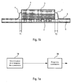
- the figure 1a illustrates by a block diagram the steps of the method according to the invention for adapting an electronic component to surface mounting.
- the example described below of implementation of the method according to the invention is illustrated for a power transistor comprising two straight connections: a straight input connection and a straight output connection.
- this example is in no way limiting: the method is suitable for any electronic power component comprising at least one connection that is not suitable for surface mounting, such as for example a straight connection.
- the method includes a step 10 in which the desired shape and dimensional characteristics of the component connections are determined. During this step 10, the shape and the dimensional characteristics of the connections are optimized according to different constraints. This optimization makes it possible to limit the performance losses that it entails.
- the method according to the invention comprises a step 20 of folding the connections of the component.
- the component connections are unsuitable for surface mounting. These connections may for example be straight connections.
- the component may be any component, for example a radiofrequency or microwave power transistor equipped with a standard flange (or "flange").
- the connections of the component are folded, for example by conformation.
- the connections are folded using for example a tool specifically developed for a type of component box, and possibly adapted to a particular application.
- This tool comprises, for example, embossings of dimensions adapted to the component and, where appropriate, to the intended application.
- the dimensions and shape of the folded connections can thus be optimized at the time of designing the circuit on which the component will be mounted.
- This tool can take the form of a press acting in cooperation with a jig (also called matrix) of folding. The use of this tool during step 20 ensures particularly precise and reproducible folding.
- the figure 1b shows by a diagram an optimized electronic component mounted on the surface of an electric circuit, said component being obtained by the implementation of the method according to the invention.
- the component shown is a microwave power transistor 3 equipped with a base 4 (or according to the English expression "flange") standard.
- the transistor 3 is connected to an electrical circuit 5 disposed on a substrate 6.
- the transistor 3 comprises an input connection 1 and an output connection 2.
- the connections 1 and 2 electrically connect the transistor 3 to the electrical circuit 5.
- the geometry of the connections 1 and 2 shown on the figure 1 b was obtained by the implementation of step 20 of the process according to the invention. Initially, the connections 1 and 2 had a geometry unsuited to surface mounting, such as a straight form.
- the connections 1 and 2 have been shaped, and in particular, folded so that the connections 1 and 2 can be mounted on the surface of the circuit 5. More precisely, the input connection 1 has been bent so that the portion of the input connection 1 (once folded) substantially parallel to the plane formed by the electric circuit 5 is equal to a distance d1 determined in step 10 for determining the length of the connections. The distance d1 is chosen minus so that it is then possible to connect the input connection 1 to the electrical circuit 5. Similarly, the output connection 2 has been bent so that the part of the connection at output 2 (once folded) substantially parallel to the plane formed by the electrical circuit 5 is equal to a distance d2 determined in step 10 for determining the length of the connections. The distance d2 is chosen at least so that it is then possible to connect the output connection 2 to the electrical circuit 5. More generally, for each component connection, the folding operation 20 and the step 10 of determining the length of the connections are performed.
- the step 10 of determining the characteristics of form and dimension of the connections fixes in particular the distance d1 and the distance d2 so that the capacitive coupling between the connections 1 and 2 and the base 4 of the component at least partially compensates for the inductive effect of folding the connections (that is to say the addition of an inductive element due to the elongation of the folded connection relative to a straight connection).
- the distance d1 is thus chosen in step 10 so that the resulting capacitive load of the distance d1 and the media / support (here air) separating the base of the housing of said connection compensates at least in part the effect inductive folding connections 1,2.
- the distance d2 is chosen in step 10 so that the resulting capacitive load of the distance d2 and the media / support (here air) separating the housing of said connection compensates for at least part of the inductive effect folding connections 1,2.
- ls 0.2 * The ⁇ ln ⁇ 2 ⁇ The / w + t + 0.2505 + w + t / 3 ⁇ The , with L, w and t respectively the length, the width and the thickness of the connection expressed in mm.
- connection considering a connection with a width of 12 mm and a thickness of 0.15 mm (which could correspond to that of a power transistor), a parasitic inductance of the order of 0.5 nH per millimeter of length is obtained. connection. In fact, the extension of such a connection of 2 mm by folding would correspond to an impedance of about 1 ohm at 1 GHz added in series in the circuit 5.
- the coupling distance, respectively d1, d2, of the connection relative to the base of the housing results in a capacitance, respectively C1, C2, of greater or lesser value, this value being inversely proportional to the distance, respectively d1 , d2.
- the distance d1 of the input connection may be chosen different from the distance d2.
- This alternative is particularly advantageous in the case where the component is a power transistor.
- This asymmetry makes it possible to optimize the respective coupling at the level of the input and output of the component.
- the capacitive coupling made for the input connection 1 (connection carrying a lower power electric current than the output connection 2) can then be chosen more important (the distance d1 being less than the distance d2) than the one realized for the output connection 2.
- the capacitive coupling made for the output connection 2 can be limited so as to eliminate the risk of electrical breakdown (or "electric flash"), due to the presence of a voltage (and a high radiofrequency power ) between the output connection 2 and the base 4, the powers and voltages at play in the output connection 2 being greater than those at the input connection 1, and the adaptation of the output component being less critical than 'entrance.
- the folding performed in step 20 and calculated in step 10 is specific to each connection 1, 2, it can be optimized to minimize the performance losses it generates (gain, bandwidth, power. ..) according to the constraints involved for each component considered.
- the transistors are subjected to much higher powers on their output than on their input (it is frequently a power deviation by a factor of 10 to 100).
- the output coupling capacitance is subjected to much higher voltage levels than that at the input of the transistor.
- the capacitive coupling at the output of the component does not generate a phenomenon of "breakdown" or electric arc between the output connection, subjected to high voltage levels, and the base of the transistor, generally connected to the circuit ground.
- the power handling at the output of the transistor depends on numerous parameters such as the moisture content of the air, the air pressure, the frequency of use of the transistor, the exact shape of the bending of the connection, as well as the circuit substrate and the mounting of the transistor connection on the circuit. Conversely, this problem does not generally arise with respect to the input coupling capability. Thus, it is conceivable to put a stronger coupling at the input than at the output without risk, which facilitates the adaptation to the input of the transistor, the latter being generally more difficult to achieve.
- the figure 2 illustrates by a diagram an optimized electronic component mounted on the surface of an electric circuit, said component being obtained by the implementation of a variant of the method according to the invention. Elements identical to the elements already presented in the other figures bear the same references.
- a piece of insulation 30 is disposed between the base 4 and the folded connection 1 and / or 2.
- the permittivity of the insulating part is chosen and taken into account during the step 10 of determining the length of the connections.
- the distances d1 and d2 as well as the material and the structure of the insulating part 30 are calculated in step 10 so that the resulting capacitive load of the distance d1 and d2 as well as the permittivity of the insulating part 30 compensates at least in part the selfic effect of folding connections (1,2).
- the capacitive coupling between the connections 1, 2 and the base 4 of the component can thus be maximized at best while keeping a greater gap between the base 4 and the connection 1, 2 folded. The performances are thus improved while minimizing the risks of short circuit during assembly and brazing of the component as well as electrical power breakdown.
- the figure 3 illustrates by a diagram an optimized electronic component mounted on the surface of an electric circuit, said component being obtained by the implementation of a variant of the method according to the invention. Elements identical to the elements already presented in the other figures bear the same references.
- the piece of insulation 30 (introduced in the variant of the method according to the invention presented at the figure 2 ) can be integrated and / or replaced by a part of a package 31 (or in the English expression "package") wrapping the component.
- the introduction of the package 31 can be performed after the step 20 of folding connections.
- the package 31 may be a plastic or molded ceramic package.
- the permittivity of the package can be taken into account during the step 10 of determining the length of the connections.
- the use of the package 31 makes it possible in particular to improve the performance of transistors dedicated to surface mounting, thus making it possible to generalize their use for a larger number of applications and power levels.
Landscapes
- Engineering & Computer Science (AREA)
- Manufacturing & Machinery (AREA)
- Microelectronics & Electronic Packaging (AREA)
- Structures For Mounting Electric Components On Printed Circuit Boards (AREA)
- Lead Frames For Integrated Circuits (AREA)
- Electric Connection Of Electric Components To Printed Circuits (AREA)
Claims (6)
- Verfahren zur Anpassung einer elektronischen Leistungskomponente, deren Verbindungen (1, 2) anfänglich nicht für eine Montage auf der Oberfläche eines Schaltkreises (5) adaptiert sind, dadurch gekennzeichnet, dass es einen Schritt (20) des Biegens der Verbindungen (1, 2) beinhaltet, wobei die Verbindungen der Komponente in dem Biegeschritt (20) so gestaltet werden, dass sie für eine Montage auf der Oberfläche eines Schaltkreises (5) adaptiert werden, wobei das Verfahren einen Schritt (10) beinhaltet, bei dem die gewünschte Gestalt und Länge der Verbindungen (1, 2) der Komponente nach dem Biegeschritt (20) ermittelt werden, wobei die Distanz (d1, d2) des Teils jeder Verbindung, die im Wesentlichen parallel zu der von dem Schaltkreis (5) gebildeten Ebene gebogen ist, so bestimmt wird, dass die kapazitive Kopplung zwischen der Verbindung (1, 2) und der Komponente den induktiven Effekt des Biegens der Verbindung (1, 2) wenigstens teilweise kompensiert.
- Verfahren nach Anspruch 1, dadurch gekennzeichnet, dass die Distanz (d1, d2) des Teils jeder Verbindung, die im Wesentlichen parallel zu der von der elektrischen Schaltung (5) gebildeten Ebene gebogen ist, so gewählt ist, dass sie proportional entgegengesetzt zu dem gewünschten kapazitiven Effekt zwischen der Verbindung (1, 2) und der Komponente ist.
- Verfahren nach einem der Ansprüche 1 und 2, dadurch gekennzeichnet, dass die Komponente wenigstens eine Eingangsverbindung (1) und eine Ausgangsverbindung (2) hat, wobei die Distanz (d1) des Teils der Eingangsverbindung (1), die im Wesentlichen parallel zu der durch die elektrische Schaltung (5) gebildeten Ebene gebogen ist, anders und kleiner ist als die Distanz (d2) des Teils der Ausgangsverbindung (2), die im Wesentlichen parallel zu der von der elektrischen Schaltung (5) gebildeten Ebene gebogen ist, wobei die Distanz (d2) des Teils der gebogenen Ausgangsverbindung so bestimmt wird, dass die Gefahr eines elektrischen Durchschlags begrenzt wird.
- Verfahren nach einem der Ansprüche 1 bis 3, dadurch gekennzeichnet, dass nach dem oder während des Schritt(es) (20) des Biegens der Verbindungen der Komponente für wenigstens eine der Verbindungen (1, 2) ein Isolierteil (30) zwischen der Komponente und der gebogenen Verbindung (1, 2) angeordnet ist, wobei die Dielektrizitätskonstante des isolierten Teils (30) so gewählt wird, dass die kapazitive Last, die aus der Distanz (d1, d2) des Teils der Verbindung (1), die im Wesentlichen parallel zu der von der elektrischen Schaltung (5) gebildeten Ebene gebogen ist, resultiert, sowie die Dielektrizitätskonstante des Isolierteils (30) den induktiven Effekt des Biegens der Verbindung (1, 2) wenigstens teilweise kompensiert.
- Verfahren nach Anspruch 4, dadurch gekennzeichnet, dass nach dem Schritt des Biegens (20) der Verbindungen der Komponente, der Isolierteil (30) integriert und/oder durch einen Teil der die Komponente schützenden Verpackung (31) ersetzt ist.
- Verfahren nach einem der vorherigen Ansprüche, dadurch gekennzeichnet, dass die Komponente ein Leistungstransistor ist.
Applications Claiming Priority (2)
| Application Number | Priority Date | Filing Date | Title |
|---|---|---|---|
| FR0610725A FR2909832A1 (fr) | 2006-12-08 | 2006-12-08 | Procede d'adaptation d'un composant electronique au montage en surface |
| PCT/EP2007/063446 WO2008068313A2 (fr) | 2006-12-08 | 2007-12-06 | Procede d'adaptation d'un composant electronique au montage en surface |
Publications (2)
| Publication Number | Publication Date |
|---|---|
| EP2103201A2 EP2103201A2 (de) | 2009-09-23 |
| EP2103201B1 true EP2103201B1 (de) | 2010-06-30 |
Family
ID=38112069
Family Applications (1)
| Application Number | Title | Priority Date | Filing Date |
|---|---|---|---|
| EP07847919A Not-in-force EP2103201B1 (de) | 2006-12-08 | 2007-12-06 | Verfahren zur anpassung einer elektronischen komponente für oberflächenanbringung |
Country Status (7)
| Country | Link |
|---|---|
| US (1) | US8316538B2 (de) |
| EP (1) | EP2103201B1 (de) |
| AT (1) | ATE472933T1 (de) |
| DE (1) | DE602007007521D1 (de) |
| ES (1) | ES2347989T3 (de) |
| FR (1) | FR2909832A1 (de) |
| WO (1) | WO2008068313A2 (de) |
Family Cites Families (6)
| Publication number | Priority date | Publication date | Assignee | Title |
|---|---|---|---|---|
| US5128834A (en) * | 1990-08-20 | 1992-07-07 | Motorola, Inc. | Surface mount receptacle for leaded components |
| JPH06104374A (ja) * | 1991-01-04 | 1994-04-15 | Internatl Business Mach Corp <Ibm> | 電子回路パッケージ並びにその導体の成形加工装置及び成形加工方法 |
| US5493259A (en) * | 1992-10-13 | 1996-02-20 | The Whitaker Corporation | High voltage, low pass filtering connector with multiple ground planes |
| DE19581837T1 (de) * | 1994-11-10 | 1997-10-02 | Micron Technology Inc | Mehrlagiger Leitungsrahmen für eine Halbleitervorrichtung |
| SE516207C2 (sv) * | 1996-11-26 | 2001-12-03 | Ericsson Telefon Ab L M | Förfarande och anordning för att ytmontera en komponent stående på en bärare |
| DE29901093U1 (de) * | 1999-01-22 | 1999-04-08 | Chu Mao Precision Industry Co., Ltd., Shen Kang Hsiang, Taichung | Fotoabtastelement-Leuchtdiode für SMD |
-
2006
- 2006-12-08 FR FR0610725A patent/FR2909832A1/fr not_active Withdrawn
-
2007
- 2007-12-06 WO PCT/EP2007/063446 patent/WO2008068313A2/fr not_active Ceased
- 2007-12-06 ES ES07847919T patent/ES2347989T3/es active Active
- 2007-12-06 DE DE602007007521T patent/DE602007007521D1/de active Active
- 2007-12-06 EP EP07847919A patent/EP2103201B1/de not_active Not-in-force
- 2007-12-06 US US12/518,244 patent/US8316538B2/en not_active Expired - Fee Related
- 2007-12-06 AT AT07847919T patent/ATE472933T1/de not_active IP Right Cessation
Also Published As
| Publication number | Publication date |
|---|---|
| WO2008068313A3 (fr) | 2008-07-24 |
| US20100115768A1 (en) | 2010-05-13 |
| EP2103201A2 (de) | 2009-09-23 |
| WO2008068313A2 (fr) | 2008-06-12 |
| ES2347989T3 (es) | 2010-11-26 |
| FR2909832A1 (fr) | 2008-06-13 |
| DE602007007521D1 (de) | 2010-08-12 |
| ATE472933T1 (de) | 2010-07-15 |
| US8316538B2 (en) | 2012-11-27 |
Similar Documents
| Publication | Publication Date | Title |
|---|---|---|
| EP0154583B1 (de) | Flossenleitungsschalter und Begrenzer im Mikrowellenbereich | |
| EP1576696A1 (de) | Antenne mit kleinem volumen insbesonderefür tragbare telefone | |
| EP2854180A1 (de) | MOS-Transistor mit Luftabstandhaltern | |
| EP3684147A1 (de) | Verbindungsstruktur für verdrahtungssubstrat und flexibles substrat sowie verpackung zur speicherung von elektronischen komponenten | |
| EP1537630B1 (de) | Elektrischer anschlusskontakt mit elastischem kontaktblatt | |
| FR3054378A3 (fr) | Antenne large bande miniature a element parasite | |
| EP0095808B1 (de) | Mikrowellen Richtungskoppler mit vier Übertragungsleitungen und in ähnlicher Weise ausgeführte passive Leistungsverteilerschaltung | |
| EP1880446A1 (de) | Verfahren für die lötfreie verbindung eines stellgliedes mit einer gedruckten schaltung, im besonderen geeignet für fahrzeugarmaturenbretter | |
| EP2103201B1 (de) | Verfahren zur anpassung einer elektronischen komponente für oberflächenanbringung | |
| JP5330359B2 (ja) | 高周波回路 | |
| FR2767237A1 (fr) | Circuit antenne ayant un circuit d'adaptation et procede de realisation | |
| EP2621027B1 (de) | Anordnung und element zur hochfrequenzverbindung und verfahren zur herstellung eines solchen elements | |
| FR2910182A1 (fr) | Perfectionnement aux antennes planaires a fente rayonnante | |
| EP3850710B1 (de) | Elektronische vorrichtung mit elastischen anschlussstiften | |
| EP2688137B1 (de) | Hyperfrequenzresonator mit Impedanzsprung, insbesondere für Hyperfrequenz-Bandsperrfilter oder -Bandpassfilter | |
| WO2018109405A1 (fr) | Module électronique de puissance | |
| EP3721504B1 (de) | Pcb-antenne, elektronische schaltung und element eines elektronischen geräts mit einer solchen antenne | |
| EP2134147B1 (de) | Verfahren zum Auflöten und Positionieren einer integrierten Schaltung auf ein Substrat und mit diesem Verfahren hergestellte Anordnung | |
| FR2651923A1 (fr) | Circuit integre de puissance. | |
| EP0274941A1 (de) | Hyperfrequenz-Halbleiteranordnung mit niedrigem Rauschen, verkapselt in einem Gehäuse | |
| WO2017203185A1 (fr) | Dispositif a haute mobilite electronique avec elements passifs integres | |
| EP0187579B1 (de) | Elektromagnetische Resonatoren und Filter mit solchen Resonatoren | |
| WO2004019448A1 (fr) | Antenne de faible volume | |
| JP2002009510A (ja) | 高周波回路及びパッケージ | |
| EP4627891A1 (de) | Filter für elektromagnetische kompatibilität und wechselrichter mit einem solchen filter |
Legal Events
| Date | Code | Title | Description |
|---|---|---|---|
| PUAI | Public reference made under article 153(3) epc to a published international application that has entered the european phase |
Free format text: ORIGINAL CODE: 0009012 |
|
| 17P | Request for examination filed |
Effective date: 20090708 |
|
| AK | Designated contracting states |
Kind code of ref document: A2 Designated state(s): AT BE BG CH CY CZ DE DK EE ES FI FR GB GR HU IE IS IT LI LT LU LV MC MT NL PL PT RO SE SI SK TR |
|
| GRAP | Despatch of communication of intention to grant a patent |
Free format text: ORIGINAL CODE: EPIDOSNIGR1 |
|
| DAX | Request for extension of the european patent (deleted) | ||
| GRAS | Grant fee paid |
Free format text: ORIGINAL CODE: EPIDOSNIGR3 |
|
| GRAA | (expected) grant |
Free format text: ORIGINAL CODE: 0009210 |
|
| AK | Designated contracting states |
Kind code of ref document: B1 Designated state(s): AT BE BG CH CY CZ DE DK EE ES FI FR GB GR HU IE IS IT LI LT LU LV MC MT NL PL PT RO SE SI SK TR |
|
| REG | Reference to a national code |
Ref country code: GB Ref legal event code: FG4D Free format text: NOT ENGLISH Ref country code: CH Ref legal event code: EP |
|
| REG | Reference to a national code |
Ref country code: IE Ref legal event code: FG4D Free format text: LANGUAGE OF EP DOCUMENT: FRENCH |
|
| REF | Corresponds to: |
Ref document number: 602007007521 Country of ref document: DE Date of ref document: 20100812 Kind code of ref document: P |
|
| REG | Reference to a national code |
Ref country code: NL Ref legal event code: VDEP Effective date: 20100630 |
|
| PG25 | Lapsed in a contracting state [announced via postgrant information from national office to epo] |
Ref country code: SE Free format text: LAPSE BECAUSE OF FAILURE TO SUBMIT A TRANSLATION OF THE DESCRIPTION OR TO PAY THE FEE WITHIN THE PRESCRIBED TIME-LIMIT Effective date: 20100630 Ref country code: LT Free format text: LAPSE BECAUSE OF FAILURE TO SUBMIT A TRANSLATION OF THE DESCRIPTION OR TO PAY THE FEE WITHIN THE PRESCRIBED TIME-LIMIT Effective date: 20100630 |
|
| LTIE | Lt: invalidation of european patent or patent extension |
Effective date: 20100630 |
|
| PG25 | Lapsed in a contracting state [announced via postgrant information from national office to epo] |
Ref country code: LV Free format text: LAPSE BECAUSE OF FAILURE TO SUBMIT A TRANSLATION OF THE DESCRIPTION OR TO PAY THE FEE WITHIN THE PRESCRIBED TIME-LIMIT Effective date: 20100630 Ref country code: FI Free format text: LAPSE BECAUSE OF FAILURE TO SUBMIT A TRANSLATION OF THE DESCRIPTION OR TO PAY THE FEE WITHIN THE PRESCRIBED TIME-LIMIT Effective date: 20100630 Ref country code: SI Free format text: LAPSE BECAUSE OF FAILURE TO SUBMIT A TRANSLATION OF THE DESCRIPTION OR TO PAY THE FEE WITHIN THE PRESCRIBED TIME-LIMIT Effective date: 20100630 Ref country code: AT Free format text: LAPSE BECAUSE OF FAILURE TO SUBMIT A TRANSLATION OF THE DESCRIPTION OR TO PAY THE FEE WITHIN THE PRESCRIBED TIME-LIMIT Effective date: 20100630 |
|
| PG25 | Lapsed in a contracting state [announced via postgrant information from national office to epo] |
Ref country code: PL Free format text: LAPSE BECAUSE OF FAILURE TO SUBMIT A TRANSLATION OF THE DESCRIPTION OR TO PAY THE FEE WITHIN THE PRESCRIBED TIME-LIMIT Effective date: 20100630 |
|
| PG25 | Lapsed in a contracting state [announced via postgrant information from national office to epo] |
Ref country code: EE Free format text: LAPSE BECAUSE OF FAILURE TO SUBMIT A TRANSLATION OF THE DESCRIPTION OR TO PAY THE FEE WITHIN THE PRESCRIBED TIME-LIMIT Effective date: 20100630 Ref country code: NL Free format text: LAPSE BECAUSE OF FAILURE TO SUBMIT A TRANSLATION OF THE DESCRIPTION OR TO PAY THE FEE WITHIN THE PRESCRIBED TIME-LIMIT Effective date: 20100630 |
|
| REG | Reference to a national code |
Ref country code: IE Ref legal event code: FD4D |
|
| PG25 | Lapsed in a contracting state [announced via postgrant information from national office to epo] |
Ref country code: CY Free format text: LAPSE BECAUSE OF FAILURE TO SUBMIT A TRANSLATION OF THE DESCRIPTION OR TO PAY THE FEE WITHIN THE PRESCRIBED TIME-LIMIT Effective date: 20100630 Ref country code: CZ Free format text: LAPSE BECAUSE OF FAILURE TO SUBMIT A TRANSLATION OF THE DESCRIPTION OR TO PAY THE FEE WITHIN THE PRESCRIBED TIME-LIMIT Effective date: 20100630 Ref country code: IS Free format text: LAPSE BECAUSE OF FAILURE TO SUBMIT A TRANSLATION OF THE DESCRIPTION OR TO PAY THE FEE WITHIN THE PRESCRIBED TIME-LIMIT Effective date: 20101030 Ref country code: PT Free format text: LAPSE BECAUSE OF FAILURE TO SUBMIT A TRANSLATION OF THE DESCRIPTION OR TO PAY THE FEE WITHIN THE PRESCRIBED TIME-LIMIT Effective date: 20101102 Ref country code: RO Free format text: LAPSE BECAUSE OF FAILURE TO SUBMIT A TRANSLATION OF THE DESCRIPTION OR TO PAY THE FEE WITHIN THE PRESCRIBED TIME-LIMIT Effective date: 20100630 Ref country code: SK Free format text: LAPSE BECAUSE OF FAILURE TO SUBMIT A TRANSLATION OF THE DESCRIPTION OR TO PAY THE FEE WITHIN THE PRESCRIBED TIME-LIMIT Effective date: 20100630 |
|
| PG25 | Lapsed in a contracting state [announced via postgrant information from national office to epo] |
Ref country code: DK Free format text: LAPSE BECAUSE OF FAILURE TO SUBMIT A TRANSLATION OF THE DESCRIPTION OR TO PAY THE FEE WITHIN THE PRESCRIBED TIME-LIMIT Effective date: 20100630 Ref country code: IE Free format text: LAPSE BECAUSE OF FAILURE TO SUBMIT A TRANSLATION OF THE DESCRIPTION OR TO PAY THE FEE WITHIN THE PRESCRIBED TIME-LIMIT Effective date: 20100630 |
|
| PLBE | No opposition filed within time limit |
Free format text: ORIGINAL CODE: 0009261 |
|
| STAA | Information on the status of an ep patent application or granted ep patent |
Free format text: STATUS: NO OPPOSITION FILED WITHIN TIME LIMIT |
|
| PG25 | Lapsed in a contracting state [announced via postgrant information from national office to epo] |
Ref country code: GR Free format text: LAPSE BECAUSE OF FAILURE TO SUBMIT A TRANSLATION OF THE DESCRIPTION OR TO PAY THE FEE WITHIN THE PRESCRIBED TIME-LIMIT Effective date: 20101001 |
|
| 26N | No opposition filed |
Effective date: 20110331 |
|
| BERE | Be: lapsed |
Owner name: THALES Effective date: 20101231 |
|
| REG | Reference to a national code |
Ref country code: DE Ref legal event code: R097 Ref document number: 602007007521 Country of ref document: DE Effective date: 20110330 |
|
| PG25 | Lapsed in a contracting state [announced via postgrant information from national office to epo] |
Ref country code: MC Free format text: LAPSE BECAUSE OF NON-PAYMENT OF DUE FEES Effective date: 20101231 |
|
| PG25 | Lapsed in a contracting state [announced via postgrant information from national office to epo] |
Ref country code: BE Free format text: LAPSE BECAUSE OF NON-PAYMENT OF DUE FEES Effective date: 20101231 |
|
| PG25 | Lapsed in a contracting state [announced via postgrant information from national office to epo] |
Ref country code: IT Free format text: LAPSE BECAUSE OF NON-PAYMENT OF DUE FEES Effective date: 20101206 Ref country code: MT Free format text: LAPSE BECAUSE OF FAILURE TO SUBMIT A TRANSLATION OF THE DESCRIPTION OR TO PAY THE FEE WITHIN THE PRESCRIBED TIME-LIMIT Effective date: 20100630 |
|
| REG | Reference to a national code |
Ref country code: CH Ref legal event code: PL |
|
| PG25 | Lapsed in a contracting state [announced via postgrant information from national office to epo] |
Ref country code: BG Free format text: LAPSE BECAUSE OF FAILURE TO SUBMIT A TRANSLATION OF THE DESCRIPTION OR TO PAY THE FEE WITHIN THE PRESCRIBED TIME-LIMIT Effective date: 20100630 Ref country code: HU Free format text: LAPSE BECAUSE OF FAILURE TO SUBMIT A TRANSLATION OF THE DESCRIPTION OR TO PAY THE FEE WITHIN THE PRESCRIBED TIME-LIMIT Effective date: 20110101 Ref country code: LU Free format text: LAPSE BECAUSE OF NON-PAYMENT OF DUE FEES Effective date: 20101206 |
|
| PG25 | Lapsed in a contracting state [announced via postgrant information from national office to epo] |
Ref country code: TR Free format text: LAPSE BECAUSE OF FAILURE TO SUBMIT A TRANSLATION OF THE DESCRIPTION OR TO PAY THE FEE WITHIN THE PRESCRIBED TIME-LIMIT Effective date: 20100630 Ref country code: CH Free format text: LAPSE BECAUSE OF NON-PAYMENT OF DUE FEES Effective date: 20111231 Ref country code: LI Free format text: LAPSE BECAUSE OF NON-PAYMENT OF DUE FEES Effective date: 20111231 |
|
| PG25 | Lapsed in a contracting state [announced via postgrant information from national office to epo] |
Ref country code: BG Free format text: LAPSE BECAUSE OF FAILURE TO SUBMIT A TRANSLATION OF THE DESCRIPTION OR TO PAY THE FEE WITHIN THE PRESCRIBED TIME-LIMIT Effective date: 20100930 |
|
| REG | Reference to a national code |
Ref country code: FR Ref legal event code: PLFP Year of fee payment: 9 |
|
| REG | Reference to a national code |
Ref country code: FR Ref legal event code: PLFP Year of fee payment: 10 |
|
| REG | Reference to a national code |
Ref country code: FR Ref legal event code: PLFP Year of fee payment: 11 |
|
| PGFP | Annual fee paid to national office [announced via postgrant information from national office to epo] |
Ref country code: DE Payment date: 20191126 Year of fee payment: 13 |
|
| PGFP | Annual fee paid to national office [announced via postgrant information from national office to epo] |
Ref country code: FR Payment date: 20191128 Year of fee payment: 13 Ref country code: IT Payment date: 20191209 Year of fee payment: 13 |
|
| PGFP | Annual fee paid to national office [announced via postgrant information from national office to epo] |
Ref country code: GB Payment date: 20191126 Year of fee payment: 13 Ref country code: ES Payment date: 20200102 Year of fee payment: 13 |
|
| REG | Reference to a national code |
Ref country code: DE Ref legal event code: R119 Ref document number: 602007007521 Country of ref document: DE |
|
| GBPC | Gb: european patent ceased through non-payment of renewal fee |
Effective date: 20201206 |
|
| PG25 | Lapsed in a contracting state [announced via postgrant information from national office to epo] |
Ref country code: FR Free format text: LAPSE BECAUSE OF NON-PAYMENT OF DUE FEES Effective date: 20201231 Ref country code: IT Free format text: LAPSE BECAUSE OF NON-PAYMENT OF DUE FEES Effective date: 20201206 |
|
| PG25 | Lapsed in a contracting state [announced via postgrant information from national office to epo] |
Ref country code: GB Free format text: LAPSE BECAUSE OF NON-PAYMENT OF DUE FEES Effective date: 20201206 Ref country code: DE Free format text: LAPSE BECAUSE OF NON-PAYMENT OF DUE FEES Effective date: 20210701 |
|
| REG | Reference to a national code |
Ref country code: ES Ref legal event code: FD2A Effective date: 20220214 |
|
| PG25 | Lapsed in a contracting state [announced via postgrant information from national office to epo] |
Ref country code: ES Free format text: LAPSE BECAUSE OF NON-PAYMENT OF DUE FEES Effective date: 20201207 |