EP2102994B1 - Elektrisch isolierte einrichtung zum koppeln von messsignalen und eine solche einrichtung umfassendes elektrisches gerät - Google Patents
Elektrisch isolierte einrichtung zum koppeln von messsignalen und eine solche einrichtung umfassendes elektrisches gerät Download PDFInfo
- Publication number
- EP2102994B1 EP2102994B1 EP07871821.0A EP07871821A EP2102994B1 EP 2102994 B1 EP2102994 B1 EP 2102994B1 EP 07871821 A EP07871821 A EP 07871821A EP 2102994 B1 EP2102994 B1 EP 2102994B1
- Authority
- EP
- European Patent Office
- Prior art keywords
- signal
- control
- transformer
- input signal
- switching means
- Prior art date
- Legal status (The legal status is an assumption and is not a legal conclusion. Google has not performed a legal analysis and makes no representation as to the accuracy of the status listed.)
- Not-in-force
Links
Images


Classifications
-
- H—ELECTRICITY
- H04—ELECTRIC COMMUNICATION TECHNIQUE
- H04B—TRANSMISSION
- H04B5/00—Near-field transmission systems, e.g. inductive or capacitive transmission systems
- H04B5/20—Near-field transmission systems, e.g. inductive or capacitive transmission systems characterised by the transmission technique; characterised by the transmission medium
- H04B5/28—Near-field transmission systems, e.g. inductive or capacitive transmission systems characterised by the transmission technique; characterised by the transmission medium using the near field of leaky cables, e.g. of leaky coaxial cables
-
- H—ELECTRICITY
- H04—ELECTRIC COMMUNICATION TECHNIQUE
- H04B—TRANSMISSION
- H04B3/00—Line transmission systems
- H04B3/02—Details
- H04B3/46—Monitoring; Testing
-
- H—ELECTRICITY
- H04—ELECTRIC COMMUNICATION TECHNIQUE
- H04B—TRANSMISSION
- H04B5/00—Near-field transmission systems, e.g. inductive or capacitive transmission systems
- H04B5/20—Near-field transmission systems, e.g. inductive or capacitive transmission systems characterised by the transmission technique; characterised by the transmission medium
- H04B5/24—Inductive coupling
- H04B5/26—Inductive coupling using coils
- H04B5/266—One coil at each side, e.g. with primary and secondary coils
-
- H—ELECTRICITY
- H04—ELECTRIC COMMUNICATION TECHNIQUE
- H04B—TRANSMISSION
- H04B5/00—Near-field transmission systems, e.g. inductive or capacitive transmission systems
- H04B5/70—Near-field transmission systems, e.g. inductive or capacitive transmission systems specially adapted for specific purposes
- H04B5/75—Near-field transmission systems, e.g. inductive or capacitive transmission systems specially adapted for specific purposes for isolation purposes
Definitions
- the invention also relates to an electrical apparatus comprising such a coupling device.
- Known electrical insulation measuring signal coupling devices are generally made with a first input signal processing part 1 and a second output signal processing part 2 SO.
- a diagram of a known device is shown on the figure 1 .
- a first input signal part 1 generally comprises a signal amplifier 3 and a modulator 4 for transferring a transformed value or a digital value of the input signal.
- the modulator 4 is generally connected to a transformer 5 or other couplers for isolating the first part 1 of the second signal processing part 2.
- the signal is processed and reconditioned in a circuit 6 to be processed as an output signal SO.
- the first part 1 receiving the input signal requires a power supply circuit 7 to operate the amplifier and the modulator.
- a first main power supply 8 supplies the output signal processing circuit 6 and an electric energy conversion circuit comprising a chopper 9 and a supply transformer 10 and the circuit 7 for provide electrical power supply to the entire first part 1.
- Some devices include transformers receiving a cut current measurement signal as shown in the documents GB1585889 AND US2003 / 0076086 .
- the control means of the signal switches are opto-electronic components which are incompatible with industrial applications having high thermal stresses. In particular, these components have characteristics of efficiency and speed which decrease very strongly when the temperature increases. These high operating temperatures are particularly present in electrical devices such as electronic trip units and electrical circuit breakers.
- the object of the invention is to provide an electrically isolated measurement signal coupling device which does not require a power supply for the input signal processing part and which can operate normally with very large temperature differences, and an apparatus comprising such a device. device.
- said means for controlling the switching means comprise coupling means by electromagnetic induction and / or by capacitive link.
- Said signal transformer has an output winding connected to detection means receiving a cut output secondary signal and providing an output signal representative of the input signal.
- the cutting of the input signal is unidirectional.
- the cutting of the input signal is bidirectional or with inversion.
- the signal transformer has two primary windings connected with inverted winding directions, a first end of each winding is connected at a common point of the windings to receive the signal input, second ends. windings are connected to first switching means and second switching means for cutting and orienting the input signal alternately on the first and second windings.
- the switching means switch input signals on the primary windings with a covering of commands at the beginning and end of switching.
- the signal transformer comprises a primary winding connected to switching means comprising four electronic switches connected in bridge with two branches, external lines of the bridge receiving the input signal and inner branches of the bridge. being connected to audit primary winding of said signal transformer, said bridge switches being alternately cross-controlled to reverse the direction of the primary signal applied to the primary winding of said signal transformer.
- the input signal is applied to a bridge of two measurement resistors connected in series, a common point of the measurement resistors being connected to a first end of a primary winding of the signal transformer, a second end of said primary winding of the signal transformer being connected to a common central part of a switching bridge with two switches of the switching means, external lines of the switches of said bridge being connected to the external parts opposite to the common point of the bridge of resistors, the two switches operating alternately to reverse the direction of the primary signal applied to the primary winding of said signal transformer.
- the detection means comprise means for filtering the cut output signal.
- the detection means comprise synchronous detection means synchronized with the control of the switching means for reconstituting an output signal representative of said input signal.
- the processing means sequentially controls the selection of the control means to provide a multiplexed output signal sequentially representative of each input signal.
- the processing means simultaneously control control means to provide an output signal representative of the sum of the input signals.
- the processing means comprise signal sampling means for sampling an output signal representative of a multiplexed secondary signal and providing values representative of each input signal, the sampling being synchronized with the selection of the means. control.
- the sampling is performed after a predetermined delay following the start of a control pulse closing switching means.
- the processing means activate the control of the control means during periods of short duration and stop the control of the control means for periods of long duration.
- said means for controlling the switching means comprise at least one control transformer having a primary winding receiving the control signals and a secondary winding for controlling switching means.
- At least one control transformer of the control means is an air transformer having a primary winding on a first face of a circuit support and a secondary winding on a second face of said circuit support.
- the circuit support is composed of a polyimide material.
- the circuit support has a thickness of between 3 and 80 ⁇ m.
- the measurement transformer is an air transformer having at least one primary winding on a first face of a circuit carrier and a secondary winding on a second face of said circuit carrier.
- the circuit support is composed of a polyimide material and has a thickness of between 3 and 80 ⁇ m.
- said at least one control transformer and at least one measuring transformer are placed on the same insulating support with windings on each side of said circuit support.
- the circuit support is composed of a polyimide material and has a thickness of between 3 and 80 ⁇ m.
- said means for controlling the switching means comprise at least two capacitive coupling capacitors each having a first electrode for receiving the control signals and a second electrode for controlling switching means.
- a circuit support composed of a polyimide material and having a thickness of between 3 and 80 ⁇ m, said circuit support has on a first face the first electrodes of said two coupling capacitors and on the second face the second electrodes of said two coupling capacitors.
- the measuring device comprises means for controlling the switching means and the switching means grouped into an electromagnetic micro-component of Mem's type.
- the device comprises an electrical shunt connected to the signal inputs for measuring an electric current, the output signal being representative of an electric current flowing in said shunt.
- the figure 2 represents a diagram of an electrical signal coupling device according to a first embodiment of the invention.
- the isolation coupling device electrical circuit comprises at least one input signal input SI, an output signal output SO representative of said input signal, and electrically isolated signal transfer means receiving the input signal and supplying said signal.
- the transfer means comprise at least one signal transformer 14 having at least one primary winding 15 for receiving a primary signal SP representative of said input signal SI.
- the input signal is cut by switching means 16 represented by a controlled switch to provide said primary signal SP representative of said input signal SI to said primary winding 15.
- the switching means 16 are controlled by control means 17 comprising an input 18 of control signals receiving control signals SC.
- An output 20 of the control means is electrically isolated from the control signal input 18 and is connected to said switching means 16 for controlling the primary signal switching at a switching frequency.
- the signal S1 is cut by the electronic switch 16 at a high switching frequency to provide on the primary winding 15 of the signal transformer 14 a cut signal SP.
- Said signal transformer 14 has an output winding 21 connected to detection means 23 receiving a cut secondary output signal SD and providing an output signal SO representative of the input signal SI.
- the secondary signal SD induced in a secondary winding 21 of the signal transformer is then processed to provide the output signal SO.
- the processing may include amplification in an amplifier 22 followed by detection and filtering in an output signal processing module 23.
- the detection can be done by simple rectification, envelope detection or synchronous rectification.
- the control signal SC of the switching means is preferably provided by a switching signal generator 24 located in the second signal processing part 2.
- the processing module 23 and the control signal generator 24 are arranged in the same processing unit 25 and fed by the same supply circuit 26.
- This supply circuit 26 can also supply the amplifier 22.
- the control signals are applied to a pulse transformer 27 of the isolated control means.
- the output of the control means may comprise a circuit signal conditioning device 28 comprising for example a diode 29 and a capacitor 30 to be adapted to the switching means 16.
- FIG 3 shows a diagram of a device according to an embodiment of the invention with a transistor switching control 31 field effect having internal diodes 32 associated in reverse. These transistors are connected in series in opposite directions, that is to say that their sources are connected together and serve as reference to the control signals supplied by the pulse transformer 27, and their control electrodes are connected together to receive said signals. Transformer control 27 through the conditioner 28. Whatever the direction or polarity of the input signal, the two transistors conduct. If no control signal is supplied, the two transistors are blocked and according to the direction or the polarity of the input signal only one of the two diodes blocks the input signal With such a scheme, the device operates whatever the polarity and the level of the input signal that can be alternating or continuous.
- a measurement or load resistor 40 is connected at the input of the device for generating the input signal SI. If the resistor 40 is an electrical shunt, the signal SI is a current measurement signal.
- the input signal has a very low voltage, for example less than 0.6 volts, a single field effect transistor 31 may suffice. In this zone, the transistor operates bidirectionally and the associated diode is not conducting in direct polarization.
- the coupling device can operate in the unidirectional input signal cutting mode by cutting the input signal in the same polarity on consecutive control commands and also applying it with the same polarity on the primary winding of the transformer. of signal.
- the cutting of the input signal can be advantageously bidirectional.
- the input signal is cut and inverted at each control command to provide on a primary induction circuit of the signal transformer 14 a primary signal having inverted consecutive induction directions.
- a magnetic coupling circuit of the signal transformer is magnetized in one direction then demagnetized and remagnetized in another direction according to the control commands to control the remanence of said magnetic circuit and improve the efficiency of the signal transfer between the primary and the secondary of the transformer 14.
- the figure 4 represents a first diagram of a coupling device according to an embodiment of the bidirectional switching invention.
- the signal transformer 14 comprises two primary windings 15A and 15B connected with inverted winding directions, a first end of each winding is connected at a common point of the windings to receive the input signal input, second ends of the windings are connected to first switching means 16A and second switching means 16B for cutting and orienting the input signal SI alternately on the first and second windings.
- the switching means switch the signals on the primary windings with a recovery of commands at the beginning and end of switching.
- the signal generator 24 provides the control signals of the switching means 16A and 16B represented by controlled switches.
- the generator 24 also provides a first synchronization signal SY to the processing module 23 for synchronous detection of the output signal. Indeed, depending on the direction of the signal on the primary, the output signal can be positive or negative. Synchronous detection makes it possible to recover a signal polarity representative of the polarity of the input signal.
- the generator 24 may also provide or receive a second synchronization signal to operate with a signal sampler. The generator, the synchronous detector, and the sampler can be part of the same circuit.
- the Figures 5A to 5G represent timing diagrams of signals in a coupling device according to the embodiment of the figure 4 .
- a curve 41 shows an input signal SI.
- the input signal SI is continuous and of positive polarity.
- the Figure 5B shows a curve 42 representative of the control of the switch 16A switching means.
- the Figure 5C shows a curve 43 representative of the control of the switch 16B switching means.
- the figure 5D shows a curve 44 representative of a current I15A in the first primary winding 15A of the signal transformer 14.
- the figure 5E shows a curve 45 representative of a current I15B in the second primary winding 15B of the signal transformer 14.
- the figure 5F shows a curve 46 representative of a current resultant 115 corresponding to currents I15A and I15B flowing in the two primary windings 15A and 15B of the signal transformer 14 controlled with reversal of direction.
- the figure 5G shows a curve 47 representative of an output signal SD on the secondary winding 21 of the transformer 14.
- the switch 16A is controlled closing while the switch 16B. just opened.
- the winding 15A receives the input signal SI. It generates a current I15A and a growing magnetic induction I15. This induction generates on the secondary of the transformer 21 an output signal equal to the derivative of the flux, therefore a positive signal SD.
- the switch 16B is controlled closing, while the switch 16A is controlled in opening.
- a current I15B flows in the winding 15B.
- Current I15A is canceled.
- the resulting magnetic induction represented by I15 decreases because winding 15B is wound in the opposite direction of winding 15A.
- the signal on the secondary of the SD transformer becomes negative.
- the alternative commutations of the switches 16A and 16B induce a magnetic induction without discontinuity in the transformer 14 and thus generate an SD signal with zero DC component.
- a switching period TC can be defined between the beginning of the conduction and the end of the conduction of a switch 16, for example between the times t1 and t2.
- the figure 6 represents a second diagram of a coupling device according to an embodiment of the bidirectional switching invention.
- the signal transformer 14 comprises a primary winding 15 connected to switching means 16 comprising four electronic switches or switches 16A1, 16A2 and 16B1, and 16B2 connected in two-armed bridge 50 and 51.
- switching means 16 comprising four electronic switches or switches 16A1, 16A2 and 16B1, and 16B2 connected in two-armed bridge 50 and 51.
- outside lines of the bridge receive the input signal SI and inner portions 53 of the branches of the bridge are connected to said primary winding 15 of the signal transformer 14.
- Said switches 16A1, 16A2 and 16B1, and 16B2 bridge are alternately controlled crosswise to reverse the direction of the primary signal SP applied to the primary winding 15 of said signal transformer 14.
- the cross-mounted switches 16A1 and 16A2 are controlled at the same time to apply the input signal in a first direction and the switches 16B1 and 16B2 in cross-editing are controlled at the same time to apply the input signal in a second direction.
- the resistor 40 may be a measurement resistor or an electrical shunt for the measurement of current signals.
- the figure 7 represents a third diagram of a coupling device according to an embodiment of the bidirectional switching invention.
- the input signal SI is applied to a bridge of two measurement resistors 40A and 40B connected in series.
- a common point 54 of the measurement resistors is connected to a first end of a primary winding 15 of the signal transformer 14, and a second end of said primary winding of the signal transformer is connected to a common central portion 55 of a bridge 56 switching circuit with two switches 16A and 16B switching means.
- External lines 57 and 58 of the switches of said bridge are connected to the outer portions 59 and 60 opposite the common point 54 of the resistor bridge.
- the two switches 16A and 16B operate alternately to invert the direction of the primary signal SP applied to the primary winding 15 of said signal transformer 14.
- a portion SIA of the signal S1 flowing in the resistor 40A and having a first sign, for example positive is applied to the winding 15.
- the switch 16B is closed and the switch 16A is open.
- a SIB portion of the signal SI present on the measurement resistor 40B and having a second negative sign opposite to the first sign is applied to the primary winding of the transformer.
- the signal on the resistor 40B is of opposite polarity to the signal on the resistor 40A since the signal reference is on the common point 54.
- FIGS. 8A to 8C represent signal curves in coupling devices according to embodiments of the bidirectional switching invention.
- a curve 65 shows an alternative SI input signal of sinusoidal form.
- a curve 66 shows an SD signal provided on a secondary of a signal transformer having a bidirectional SP primary signal control.
- a curve 67 shows an output signal SO processed so as to reconstruct a sinusoidal signal representative of the input signal.
- the processing means detect the bidirectional signal by rectifying the signal synchronously, for example with electronic switch bridges or electronic circuits with sampling and programmed processing.
- the detection means comprise means for filtering the cut output signal and / or synchronous detection means synchronized with the control of the switching means for reconstituting an output signal representative of said input signal.
- the processing means 25 can activate control of the control means for periods of short duration and stop the control of the control means during longer periods of inactivity. For example, in the diagram of the figure 6 cross-mounted switches 16A1 and 16A2 are controlled for a first period. Then, for a second period, switches 16B1 and 16B2 are controlled while switches 16A1 and 16A2 are turned off. Finally, for all switches, the command is stopped during a third period. Preferably, the first and second periods are shorter than the third period.
- the periods can be regular in a cycle or in a duty cycle predetermined or randomly controlled according to the needs of the processing means.
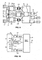
- the figure 9 represents an embodiment of an electrical signal coupling device according to an embodiment of the invention of the diagram of the figure 7 .
- the measurement resistor 40 is an electrical shunt for measuring the electric current.
- the output signal SO is then representative of an electric current flowing in said shunt.
- the shunt has a midpoint 54 separating a first portion 40A and a second portion 40B on each side of the midpoint.
- the shunt comprises power connection pads for circulating the measurement current and three measurement links.
- a common link 72 is connected to point 54 of the shunt, a first external link 73 is connected on the side of the first portion 40A and a second external link 74 is connected on the side of the second portion 40B.
- the switching means such as the electronic switches 16A and 16B and other ancillary components such as the conditioning circuits 28 are arranged on a first printed circuit 80 to the electric potential of a circuit to be measured.
- This circuit 80 receives the connections with the shunt and links with the primary of the signal transformer 14 and links with pulse transformers 27A and 27B of the control means 17.
- a second printed circuit 81 supports circuits of the unit such as the detection and processing circuits 23 and the control signal generators 24.
- the electronic circuits on the printed circuit 81 are at a different potential and decoupled electrically and galvanically with respect to the electronic circuits arranged on the printed circuit 80.
- the printed circuit 81 has on one side links with the signal transformer 14 and the transformers pulses 27A and 27B and on the other side of the connections with a supply input P 82, a signal output 83 SO and a common ground input 0V 84.
- the signal transformer is part of a multiplexing set.
- the figure 10 represents a first diagram of a coupling device according to an embodiment of the invention with a multiplexing of input signals on a common signal transformer 14.
- the signal transformer 14 comprises: at least a first primary winding 151 for receiving a first input signal SI1 and at least first switching means 161 for cutting said first input signal SI1 and at least one second primary winding 152 to receive a second input signal SI2 and at least second means 162 switching circuit for cutting said second input signal SI2, and at least one secondary winding 21 for providing a secondary signal SD of representative of said first input signal SI1 or said second input signal SI2.
- a processing unit 25 selects first control means 271 of said first switching means 161 to provide a representative SO output signal of said first input signal SI1, or selects second control means 272 of the second switching means 162 to provide an output signal SO representative of said second input signal SI2.
- first control means 271 of said first switching means 161 to provide a representative SO output signal of said first input signal SI1
- second control means 272 of the second switching means 162 to provide an output signal SO representative of said second input signal SI2.
- the figure 11 represents a second diagram of a coupling device according to an embodiment of the invention with a multiplexing of input signals SI1, SI2, SI3, SI4 on a common signal transformer 14.
- the four signals SI1 to SI4 can be generated on measuring resistances 401, 402, 403, or 404 then cut by switching means respectively 161, 162, 163, and 164 and controlled by pulse transformers respectively 271, 272, 273 and 274 control means
- the switching means 274 are completely represented in one part while the others are represented by two-part blocks to simplify the scheme.
- the cutting of the input signals makes it possible to supply primary signals SP1, SP2, SP3, and SP4 to primary windings 151, 152, 153, and 154 of the signal transformer 14.
- the galvanic or electrical isolation is represented by a interrupted line 86.
- the secondary signal SD is applied to an amplifier 22 having a parameterizable amplification.
- the output signal of the amplifier is filtered by a low-pass filter 87 before being applied to the processing unit 25.
- the processing unit 25 comprises a signal sampler 88 for sampling a signal representative of a signal multiplexed secondary and provide values representative of each input signal, the sampling being synchronized with the selection of the control means.
- the amplifier 22 and the sampler 88 are referenced by a reference circuit 89.
- a microcontroller or a microprocessor located in the processing unit allows the supply of control signals of the switching means and the synchronization of the sampling serving as synchronous detection.
- the microprocessor 90 receiving the samples of the signal SD separates the different values into several output signals SO1, SO2, SO3 and SO4 representative respectively of the input signals SI1, SI2, SI3, and SI4.
- the processing means sequentially controls the selection of the control means to provide a sequentially representative multiplexed SO output signal of each input signal SI1 to SI4.
- the processing means can simultaneously control control means for providing an output signal SO representative of the sum of the input signals.
- the coupling device can be used in a four-pole type circuit breaker receiving signals representative of three-phase signals and a neutral conductor.
- the measuring resistors 401, 402, 403, or 404 are then current measurement shunts.
- a simultaneous control of the four channels can provide a signal SO representative of a differential current.
- simultaneous digital processing of the four channels by a processor may provide a signal SO representative of a differential current or the sum of the input signals.
- the Figures 12A to 12G represent signal curves in a device of the figure 11 . States of the different switching means 161 to 164 are represented on curves 91 to 94 of FIG. figure 12A . State 1 corresponds to a closed state of the corresponding switch and state 0 corresponds to the open state.
- the figure 12B shows a curve 95 representative of an example of an input signal SI1.
- the figure 12C shows a curve 96 representative of an example of an input signal SI2.
- the figure 12D shows a curve 97 representative of an example of an input signal SI3.
- the figure 12E shows a curve 98 representative of an example of an input signal SI4.
- the figure 12F shows a curve 99 representative of an example of secondary signal SD.
- the figure 12G shows a sampling of the secondary signal to separate the SD signal into four output signals SO1, SO2, SO3 and SO4 representative of the four input signals SI1, SI2, SI3, and SI4.
- the switch 161 is closed and the secondary signal SD becomes representative of the input signal SI1.
- the signal SD is sampled to have an output signal SO1 representative of the signal SI1.
- the switch 162 is closed and the secondary signal SD becomes representative of the input signal SI2.
- the signal SD is sampled to have an output signal SO2 representative of the signal SI2.
- the control of the switch 162 is completed.
- the switch 163 is closed and the secondary signal SD becomes representative of the input signal SI3.
- the signal SD is sampled to have an output signal SO3 representative of the signal SI3.
- the control of the switch 163 is completed.
- the switch 164 is closed and the secondary signal SD becomes representative of the input signal SI4.
- the signal SD is sampled to have an output signal SO4 representative of the signal SI4.
- the control of the switch 164 is complete.
- the cycle begins again by closing the switch 161, and sampling SD at time t14 to provide SO1.
- the delay D corresponds to the waiting time between the start of closing of the switches and the sampling of the secondary signal SD at the output of the signal transformer 14.
- the figure 13 represents a flow chart showing an acquisition cycle of a measurement sample.
- the processing unit selects the path to be measured. Then, in a step 101, an electronic switch of the switching means is closed. Then, after a delay D allowing the stabilization of the operation of the transformer, in particular avoiding parasitic oscillations at a step 102, the processing unit controls the sampling of a signal representative of the secondary signal SD at a step 103. sampling is performed after a predetermined delay D following the start of a control pulse closing switch means.
- the figure 14 represents an electrical apparatus diagram comprising a measuring device according to an embodiment of the invention.
- Such an electrical apparatus 104 comprises at least a measuring resistor 401 and 402, electrical power contacts 105 connected in series with said at least one measurement resistor, a mechanism 106 for opening the electrical contacts 105, and processing means 107 for protecting functions a relay 108 connected to said mechanism 106.
- the apparatus comprises a coupling device 110 as described above having at least one signal input connected to said at least one measuring resistor, and a signal output connected to the protection function processing means 107 for providing an output signal SO representative of a current flowing in said measurement resistor.
- the coupling device 110 may be the same as that of the figure 10 with signal multiplexing.
- Resistors 401 and 402 may be resistors of very low values such as electric shunts.
- control means of the switching means are preferably pulse transformers 27, 271, 272 having a primary winding 115 receiving the control signals and a secondary winding 116 for controlling means of switching. switching.
- the figure 15 represents a pulse transformer in printed form used in the control means of a coupling device according to an embodiment of the invention.
- the pulse transformer is an air transformer having a primary winding 115 on a first face 117 of a printed circuit 118 and a secondary winding 116 on a second face 119 of said printed circuit.
- the operating frequency is then very high to achieve very small winding sizes.
- each winding has thirteen turns with an outer dimension less than one centimeter on the side.
- the operating frequency of the control means is much greater than the switching frequency.
- the signals of control are then pulses or bursts of high frequency pulses provided during TC switching periods.
- the printed circuit may also be an etched circuit or any other circuit serving as support for example a ceramic support or alumina. Even in the printed form, the control transformers may have a magnetic circuit adapted to the shapes and dimensions of the circuit support.
- a circuit support 118 is advantageously composed of a polyimide material.
- the circuit support has a thickness (E) of between 3 and 80 ⁇ m.
- the measuring transformer may be an air transformer having at least one primary winding 15 on a first face of a circuit support 118 and a secondary winding 21 on a second face of said circuit support.
- the circuit support is composed of a polyimide material having a thickness (E) of between 3 and 80 ⁇ m.
- the figure 16 shows an assembly of two control transformers and a measurement transformer placed on the same insulating support with windings on each side of said circuit support.
- the circuit support is advantageously composed of a polyimide material having a thickness (E) of between 3 and 80 ⁇ m.
- FIGS 17 and 18 show variants of devices according to embodiments of the invention.
- the control means of the switching means are a double capacitive link 120 passing the pulses and blocking the DC or low frequency to ensure the galvanic isolation.
- the control signals are complementary to circulate a control current between the two links and ensure a common mode electrical isolation.
- said control means of the switching means comprise at least two capacitive coupling capacitors 501, 502 each having a first electrode 503 for receiving the control signals and a second electrode 504 for controlling switching means.
- the capacitors are made on a circuit support 505 composed of a polyimide material having a thickness of between 3 and 80 microns.
- said circuit support has on a first face the first electrodes 503 and on the second face the second electrodes 504 of said two coupling capacitors 501 and 502.
- control means of the switching means and the switching means are grouped into a micro electromagnetic component 122, preferably in the so-called MEMs technology.
- switching means may be used in particular field effect transistors, bipolar transistors, electromagnetically controlled switches, electrostatic or optical.
- the switching frequency of the input signal SI may depend on the size of the coupling transformer used and the transfer rate through said transformer. This switching frequency is advantageously related to the capabilities of the detection and sampling means.
- the coupling devices described above make it possible to measure any type of electrical signals, in particular currents, voltages, or several types in multiplexed mode on the same magnetic circuit of the signal transformer.
- the input signal can be provided by a voltage divider bridge.
- the electrical apparatus comprising the coupling device can be of any type. If the electrical apparatus includes electrical protection functions such as those of a relay or a circuit breaker trip, the measurement resistors are advantageously electric shunts. These shunts may be of the resistor or impedance type, for example inductance type.
Landscapes
- Engineering & Computer Science (AREA)
- Computer Networks & Wireless Communication (AREA)
- Signal Processing (AREA)
- Measurement Of Current Or Voltage (AREA)
- Testing Relating To Insulation (AREA)
Claims (15)
- Kopplungsvorrichtung mit elektrischer Isolation, die Folgendes umfasst:- mindestens einen Eingangssignaleingang (SI)dadurch gekennzeichnet, dass die Steuermittel der Umschaltmittel Kopplungsmittel durch elektromagnetische Induktion und/oder durch kapazitive Verbindung umfassen.- einen Ausgangssignalausgang (SO), der für das Eingangssignal repräsentativ ist, und- Signaltransfermittel mit elektrischer Isolation, die das Eingangssignal empfangen und das Ausgangssignal liefern,- mindestens einen Signaltransformator (14), der mindestens eine Primärwicklung (15, 15A, 15B, 151, 152, 153, 154) hat, um ein Primärsignal (SP, SP1, SP2, SP3, SP4) zu empfangen, das für das Eingangssignal (SI, SIA, SIB, SI1, SI2, SI3, SI4) repräsentativ ist,- Umschaltmittel (16, 16A, 16B, 161, 162, 163, 164, 31, 32), um das Eingangssignal zu teilen und das Primärsignal, das für das Eingangssignal repräsentativ ist, zu der Primärwicklung zu liefern,- Steuermittel (17, 17A, 17B, 27, 27A, 27B, 271, 272, 273, 274) der Umschaltmittel, die einen Steuersignaleingang (SC) umfassen, der Steuersignale während der Umschaltzeitspannen (TC) empfängt, und einen elektrisch von dem Steuersignaleingang isolierten Ausgang, der mit den Umschaltmitteln (16, 16A, 16B, 161, 162, 163, 164, 31, 32) verbunden ist, um das Primärsignalteilen während der Umschaltzeitspannen (TC) zu steuern,
- Kopplungsvorrichtung nach Anspruch 1, dadurch gekennzeichnet, dass der Signaltransformator (14) zwei Primärwicklungen (15A, 15B) umfasst, die mit umgekehrten Wicklungsrichtungen angeschlossen sind, wobei ein erstes Ende jeder Wicklung an einer gemeinsamen Stelle der Wicklungen verbunden ist, um das Eingangssignal zu empfangen, wobei zweite Enden der Wicklungen mit ersten Umschaltmitteln (16A) und mit zweiten Umschaltmitteln (16B) verbunden sind, um das Eingangssignal (SI, SIA, SIB) zu teilen und abwechselnd auf die erste und die zweite Wicklung auszurichten.
- Kopplungsvorrichtung nach Anspruch 1, dadurch gekennzeichnet, dass der Signaltransformator (14) eine Primärwicklung (15) umfasst, die mit Umschaltmitteln (16) verbunden ist, die vier elektronische Umschalter (16A1, 16A2, 16B1, 16B2) umfassen, die als Brücke mit zwei Schenkeln (50, 51) verbunden sind, wobei externe Leitungen der Brücke das Eingangssignal (SI) empfangen und innere Schenkel (53) der Brücke mit der Primärwicklung (15) des Signaltransformators verbunden sind, wobei die Umschalter in Brücke abwechselnd gekreuzt gesteuert werden, um die Richtung des Primärsignals (SP), das an die Primärwicklung (15) des Signaltransformators angelegt wird, umzukehren.
- Kopplungsvorrichtung nach Anspruch 1, dadurch gekennzeichnet, dass das Eingangssignal (SI, SIA, SIB) an eine Brücke aus zwei Messwiderständen (40A, 40B), die in Serie geschaltet sind, angelegt ist, wobei eine gemeinsame Stelle (54) der Messwiderstände mit einem ersten Ende einer Primärwicklung (15) des Signaltransformators (14) verbunden ist, wobei ein zweites Ende der Primärwicklung (15) des Signaltransformators mit einem gemeinsamen zentralen Teil (55) einer Umschaltbrücke mit zwei Umschaltern (16A, 16B) der Umschaltmittel verbunden ist, wobei externe Leitungen (57, 58) der Umschalter der Brücke mit den externen Teilen (59, 60), die der gemeinsamen Stelle der Widerständebrücke entgegengesetzt sind, verbunden sind, wobei die zwei Umschalter abwechselnd funktionieren, um die Richtung des Primärsignals (SP), das an die Primärwicklung (15) des Signaltransformators (14) angelegt ist, umzukehren.
- Kopplungsvorrichtung nach einem der Ansprüche 1 bis 4, dadurch gekennzeichnet, dass der Signaltransformator (14) Folgendes umfasst:- mindestens eine erste Primärwicklung (151), um ein erstes Eingangssignal (S11) zu empfangen, und mindestens erste Umschaltmittel (161), um das erste Eingangssignal zu teilen,- mindestens eine zweite Primärwicklung (152), um ein zweites Eingangssignal (SI2) zu empfangen, und mindestens zweite Umschaltmittel (162), um das zweite Eingangssignal zu teilen, und- mindestens eine Sekundärwicklung (21), um ein Signal (SD), das für das erste Eingangssignal (SI1) oder das zweite Eingangssignal (SI2) repräsentativ ist, zu liefern.
- Kopplungsvorrichtung nach Anspruch 5, dadurch gekennzeichnet, dass sie Verarbeitungsmittel (25) umfasst:- um erste Steuermittel (271) der ersten Umschaltmittel (161) auszuwählen, um ein Ausgangssignal (SO), das für das erste Eingangssignal (SI1) repräsentativ ist, zu liefern, oder- um zweite Steuermittel (272) der zweiten Umschaltmittel (162) auszuwählen, um ein Ausgangssignal (SO), das für das zweite Eingangssignal (SI2) repräsentativ ist, zu liefern.
- Kopplungsvorrichtung nach einem der Ansprüche 5 oder 6, dadurch gekennzeichnet, dass die Verarbeitungsmittel (25) die Auswahl der Steuermittel sequenziell steuern, um ein gemultiplextes Ausgangssignal (SO) zu liefern, das sequenziell für jedes Eingangssignal (SI1, SI2, SI3, SI4) repräsentativ ist, und/oder gleichzeitig Steuermittel steuern, um ein Ausgangssignal (SO) zu liefern, das für die Summe der Eingangssignale repräsentativ ist.
- Kopplungsvorrichtung nach einem der Ansprüche 5 bis 7, dadurch gekennzeichnet, dass die Verarbeitungsmittel (25) das Steuern der Steuermittel während Perioden mit kurzer Dauer aktivieren und das Steuern der Steuermittel während Perioden mit langer Dauer stoppen.
- Kopplungsvorrichtung nach einem der Ansprüche 1 bis 8, dadurch gekennzeichnet, dass die Steuermittel der Umschaltmittel mindestens einen Steuertransformator (27, 271, 272, 273, 274, 27A, 27B) umfassen, der eine Primärwicklung hat, die die Steuersignale empfängt, und eine Sekundärwicklung, um Umschaltmittel zu steuern, wobei der Transformator ein Luftkerntransformator ist, der eine Primärwicklung (115) auf einer ersten Seite (117) eines Schaltungsträgers (118) und eine Sekundärwicklung (116) auf einer zweiten Seite (119) des Schaltungsträgers hat.
- Kopplungsvorrichtung nach Anspruch 9, dadurch gekennzeichnet, dass der Schaltungsträger aus einem Polyimid-Werkstoff besteht, der eine Stärke (E) zwischen 3 und 80 µm hat.
- Kopplungsvorrichtung nach einem der Ansprüche 1 bis 10, dadurch gekennzeichnet, dass der Messtransformator ein Luftkerntransformator ist, der mindestens eine Primärwicklung (15) auf einer ersten Seite (117) eines Schaltungsträgers (118) und eine Sekundärwicklung (21) auf einer zweiten Seite (119) des Schaltungsträgers hat, wobei der Schaltungsträger aus einem Polyimid-Werkstoff besteht, der eine Stärke (E) zwischen 3 und 80 µm hat.
- Kopplungsvorrichtung nach einem der Ansprüche 9 bis 11, dadurch gekennzeichnet, dass der mindestens eine Steuertransformator (371, 372) und mindestens eine Messtransformator (14) auf ein und demselben isolierenden Träger (118) mit Wicklungen (116, 116, 15, 21) auf jeder Seite des Schaltungsträgers platziert sind, wobei der Schaltungsträger aus einem Polyimid-Werkstoff mit einer Stärke (E) zwischen 3 und 80 µm besteht.
- Kopplungsvorrichtung nach einem der Ansprüche 1 bis 12, dadurch gekennzeichnet, dass die Steuermittel der Umschaltmittel mindestens zwei kapazitive Kopplungskondensatoren (501, 502) umfassen, die jeweils eine erste Elektrode (503) zum Empfangen der Steuersignale und eine zweite Elektrode (504) zum Steuern der Umschaltmittel haben.
- Kopplungsvorrichtung nach einem der Ansprüche 1 bis 13, dadurch gekennzeichnet, dass sie auch Steuermittel der Umschaltmittel (17) und die Umschaltmittel (16) umfasst, die in einem elektromagnetischen Mikrobauteil (122) des Typs MEMS gruppiert sind.
- Elektrogerät, das Folgendes umfasst:- mindestens einen Messwiderstand (40, 40A, 40B, 401, 402),- elektrische Leistungskontakte (105), die mit dem mindestens einen Messwiderstand in Serie geschaltet sind,- einen Steuermechanismus (106) zum Öffnen der elektrischen Kontakte, und- Verarbeitungsmittel (107) mit Schutzfunktionen, die ein Relais (108), das mit dem Mechanismus verbunden ist, steuern,dadurch gekennzeichnet, dass es mindestens eine Kopplungsvorrichtung nach einem der Ansprüche 1 bis 14 umfasst, die Folgendes hat:- mindestens einen Signaleingang (SI1, SI2), der mit dem mindestens einen Messwiderstand (40, 40A, 40B, 401, 402) verbunden ist, und- einen Signalausgang (SO), der mit Schutzfunktions-Verarbeitungsmitteln (25) verbunden ist, um ein Signal (SO), das für einen Strom, der in dem mindestens einen Messwiderstand zirkuliert, repräsentativ ist, zu liefern.
Applications Claiming Priority (2)
| Application Number | Priority Date | Filing Date | Title |
|---|---|---|---|
| FR0611006A FR2910162B1 (fr) | 2006-12-18 | 2006-12-18 | Dispositif de couplage de signal de mesure a isolation electrique et appareil electrique comportant un tel dispositif |
| PCT/FR2007/002026 WO2008087276A2 (fr) | 2006-12-18 | 2007-12-10 | Dispositif de couplage de signal de mesure a isolation electrique et appareil electrique comportant un tel dispositif |
Publications (2)
| Publication Number | Publication Date |
|---|---|
| EP2102994A2 EP2102994A2 (de) | 2009-09-23 |
| EP2102994B1 true EP2102994B1 (de) | 2015-11-11 |
Family
ID=38234338
Family Applications (1)
| Application Number | Title | Priority Date | Filing Date |
|---|---|---|---|
| EP07871821.0A Not-in-force EP2102994B1 (de) | 2006-12-18 | 2007-12-10 | Elektrisch isolierte einrichtung zum koppeln von messsignalen und eine solche einrichtung umfassendes elektrisches gerät |
Country Status (7)
| Country | Link |
|---|---|
| US (1) | US8390270B2 (de) |
| EP (1) | EP2102994B1 (de) |
| CN (1) | CN101563856B (de) |
| BR (1) | BRPI0721075B1 (de) |
| ES (1) | ES2558878T3 (de) |
| FR (1) | FR2910162B1 (de) |
| WO (1) | WO2008087276A2 (de) |
Families Citing this family (12)
| Publication number | Priority date | Publication date | Assignee | Title |
|---|---|---|---|---|
| FR2910173B1 (fr) * | 2006-12-18 | 2012-05-04 | Schneider Electric Ind Sas | Dispositif de mesure de courant a isolation electrique, declencheur electronique, et disjoncteur comportant un tel dispositif |
| US7889041B2 (en) * | 2007-11-05 | 2011-02-15 | Schweitzer Engineering Laboratories, Inc. | Systems and methods for forming an isolated transformer |
| CN102804619B (zh) | 2010-03-09 | 2014-07-09 | 丰田自动车株式会社 | 信号传输装置 |
| US20120085176A1 (en) * | 2010-10-07 | 2012-04-12 | Ray Morales | Analog strain gauge conditioning system for space environment |
| WO2016048423A1 (en) | 2014-09-24 | 2016-03-31 | Analog Devices, Inc. | Circuits and systems for multiplexed isolator communication |
| CN105807117B (zh) * | 2014-12-29 | 2020-01-31 | 苏州普源精电科技有限公司 | 用于电流测量探头的电流感测电路及其电流测量探头 |
| US9829531B2 (en) * | 2015-10-23 | 2017-11-28 | Maxim Integrated Products, Inc. | Dual galvanic isolation barriers and monitoring systems and methods |
| EP3431978B1 (de) * | 2017-07-17 | 2020-09-02 | Mettler-Toledo GmbH | Verfahren und vorrichtung zur überwachung und/oder zur bestimmung des zustands einer messsonde |
| CN109347522B (zh) * | 2018-09-20 | 2021-09-28 | 刘泰康 | 基于磁力线媒介的电磁感应式信息隔离传输系统 |
| JP7101152B2 (ja) | 2019-09-06 | 2022-07-14 | 株式会社東芝 | 電子回路、電流計測装置、および方法 |
| JP7542338B2 (ja) | 2020-07-02 | 2024-08-30 | 株式会社東芝 | 電子回路、電流計測装置、電圧計測装置、電力変換器、およびインバータ |
| JP2024038891A (ja) | 2022-09-08 | 2024-03-21 | 株式会社東芝 | 電子回路及び電力変換器 |
Family Cites Families (17)
| Publication number | Priority date | Publication date | Assignee | Title |
|---|---|---|---|---|
| US3667289A (en) * | 1970-01-05 | 1972-06-06 | Saab Scania Ab | Apparatus for testing automobiles |
| US4042871A (en) * | 1975-11-14 | 1977-08-16 | Ecc Corporation | Conversion system with overcurrent protection and start-up circuitry |
| DE2636677A1 (de) * | 1976-08-14 | 1978-02-16 | Bosch Gmbh Robert | Messeinrichtung zur digitalen messung von kenndaten von zuendanlagen fuer brennkraftmaschinen |
| HU196513B (en) * | 1985-11-18 | 1988-11-28 | Miki Merestechnikai Fejlesztoe | Apparatus for measuring voltage by sampling |
| DE68924112T2 (de) * | 1988-08-24 | 1996-04-18 | Lem Liaisons Electron Mec | Stromsensor. |
| FR2664442B1 (fr) * | 1990-07-03 | 1996-04-26 | Merlin Gerin | Declencheur electronique comportant une fonction long retard amelioree. |
| FR2690752A1 (fr) * | 1992-04-30 | 1993-11-05 | Artus | Appareil d'acquisition multivoies de grandeurs électriques. |
| FR2725320B1 (fr) * | 1994-09-29 | 1996-10-31 | Schneider Electric Sa | Dispositif de declenchement comportant au moins un transformateur de courant |
| FR2757699B1 (fr) * | 1996-12-23 | 1999-01-29 | Schneider Electric Sa | Declencheur electronique comportant, en serie, des filtres a reponse impulsionnelle finie et infinie |
| FR2762156B1 (fr) * | 1997-04-15 | 1999-06-11 | Schneider Electric Sa | Declencheur electronique selectif, disjoncteur comportant un tel declencheur et procede de declenchement selectif |
| US6259246B1 (en) * | 1999-05-04 | 2001-07-10 | Eaton Corporation | Load sensing apparatus and method |
| JP4269515B2 (ja) * | 2000-12-25 | 2009-05-27 | パナソニック電工株式会社 | 電気量検出センサ |
| FR2830386B1 (fr) * | 2001-10-02 | 2003-12-05 | Schneider Electric Ind Sa | Dispositif de couplage pour un systeme de transmission a courant porteur a bas debit |
| US7259545B2 (en) * | 2003-02-11 | 2007-08-21 | Allegro Microsystems, Inc. | Integrated sensor |
| US6885184B1 (en) * | 2004-03-31 | 2005-04-26 | Asco Power Technologies, L.P. | Galvanically isolated voltage sensing circuit |
| FR2891093B1 (fr) * | 2005-09-16 | 2007-10-26 | Schneider Electric Ind Sas | Declencheur electronique pourvu de moyens de surveillance, disjoncteur comportant un tel declencheur et procede de surveillance. |
| US7876086B2 (en) * | 2008-02-28 | 2011-01-25 | International Components Corporation | Current measuring device for measuring the electrical current flowing in an electrical conductor electrically isolated from the current measuring device |
-
2006
- 2006-12-18 FR FR0611006A patent/FR2910162B1/fr not_active Expired - Fee Related
-
2007
- 2007-12-10 ES ES07871821.0T patent/ES2558878T3/es active Active
- 2007-12-10 WO PCT/FR2007/002026 patent/WO2008087276A2/fr not_active Ceased
- 2007-12-10 CN CN2007800466353A patent/CN101563856B/zh not_active Expired - Fee Related
- 2007-12-10 BR BRPI0721075A patent/BRPI0721075B1/pt not_active IP Right Cessation
- 2007-12-10 US US12/312,675 patent/US8390270B2/en active Active
- 2007-12-10 EP EP07871821.0A patent/EP2102994B1/de not_active Not-in-force
Also Published As
| Publication number | Publication date |
|---|---|
| BRPI0721075A2 (pt) | 2014-04-15 |
| WO2008087276A2 (fr) | 2008-07-24 |
| FR2910162B1 (fr) | 2009-12-11 |
| CN101563856B (zh) | 2013-11-13 |
| BRPI0721075B1 (pt) | 2020-02-04 |
| WO2008087276A3 (fr) | 2008-10-30 |
| ES2558878T3 (es) | 2016-02-09 |
| FR2910162A1 (fr) | 2008-06-20 |
| EP2102994A2 (de) | 2009-09-23 |
| CN101563856A (zh) | 2009-10-21 |
| US20100060261A1 (en) | 2010-03-11 |
| US8390270B2 (en) | 2013-03-05 |
Similar Documents
| Publication | Publication Date | Title |
|---|---|---|
| EP2102994B1 (de) | Elektrisch isolierte einrichtung zum koppeln von messsignalen und eine solche einrichtung umfassendes elektrisches gerät | |
| EP2102668A2 (de) | Elektrisch isolierte strommessungsvorrichtung, elektronischer auslöser sowie schutzschalter mit derartiger vorrichtung | |
| EP3232526B1 (de) | Vorrichtung zur detektion eines fehlerstroms | |
| EP0629036B1 (de) | Anordnung zur Zuführung einer Spannung an eine elektronische Schaltung, besonders an eine elektronische Schaltung eines Stromsensors der auf einer elektrischen Leitung geschaltet ist | |
| EP3457510B1 (de) | Elektrischer anschluss, der ein elektrisches schutzsystem umfasst | |
| EP0082071A1 (de) | Einrichtung für die Umschaltung einer mit mindestens einem gesteuerten Schalter versehenen Gleichspannungsquelle und Kommutierungshilfsschaltung für eine solche Einrichtung | |
| EP0019507B1 (de) | Verbesserung kapazitiver Spannungstransformatoren mit elektronischem Ausgang | |
| EP3075067B1 (de) | Steuerungsschaltung für einen leistungswandler | |
| FR2568715A1 (fr) | Dispositif de commande d'une bobine d'electroaimant et appareil electrique de commutation equipe d'un tel dispositif | |
| EP3561523B1 (de) | Elektrische vorrichtung, die mittel zum prüfen eines prüfbaren stromwandlers umfasst | |
| FR2871627A1 (fr) | Relais a l'etat solide pour la commutation d'une alimentation en alternatif vers une charge reactive et procede pour faire fonctionner un tel relais | |
| CH621895A5 (de) | ||
| EP0652636A1 (de) | H-Brückenleistungsverstärker und Einrichtung zum Schalter desselben | |
| EP1139361B1 (de) | Elektrische Schaltungsanordnung zur Meldung von Zustandsinformationen, insbesondere für Eisenbahnmaterial, und System mit einer solchen Einrichtung | |
| EP3938792B1 (de) | Elektrische anlage mit einem überwachungsmodul | |
| EP1450474A2 (de) | Wandler und direkte Energieübertragung | |
| EP0617292B1 (de) | System zur ständigen Überwachung der elektrischen Leitfähigkeit eines Wechselstromnetzes | |
| EP3938793B1 (de) | Elektrische anlage mit einem überwachungsmodul | |
| EP2198507B1 (de) | Variable steuerung | |
| EP0196934B1 (de) | Steuerschaltung für Taktversorgung für verschiedene Anwendungen | |
| EP1629598B1 (de) | Statische sichere ausgabestufe | |
| CH653496A5 (fr) | Circuit d'alimentation a tension reglable. | |
| EP3139485A1 (de) | Progressives anlassverfahren eines elektromotors | |
| FR2808631A1 (fr) | Dispositif d'entree logique pour automate | |
| EP1330865A1 (de) | Verfahren und schaltungsanordung zur pulssteuerung eines leistungsbauelementes |
Legal Events
| Date | Code | Title | Description |
|---|---|---|---|
| PUAI | Public reference made under article 153(3) epc to a published international application that has entered the european phase |
Free format text: ORIGINAL CODE: 0009012 |
|
| 17P | Request for examination filed |
Effective date: 20090507 |
|
| AK | Designated contracting states |
Kind code of ref document: A2 Designated state(s): AT BE BG CH CY CZ DE DK EE ES FI FR GB GR HU IE IS IT LI LT LU LV MC MT NL PL PT RO SE SI SK TR |
|
| DAX | Request for extension of the european patent (deleted) | ||
| 17Q | First examination report despatched |
Effective date: 20130320 |
|
| GRAP | Despatch of communication of intention to grant a patent |
Free format text: ORIGINAL CODE: EPIDOSNIGR1 |
|
| GRAJ | Information related to disapproval of communication of intention to grant by the applicant or resumption of examination proceedings by the epo deleted |
Free format text: ORIGINAL CODE: EPIDOSDIGR1 |
|
| GRAP | Despatch of communication of intention to grant a patent |
Free format text: ORIGINAL CODE: EPIDOSNIGR1 |
|
| RIC1 | Information provided on ipc code assigned before grant |
Ipc: G08C 17/02 20060101ALI20150522BHEP Ipc: H04B 5/00 20060101AFI20150522BHEP Ipc: H04B 3/46 20150101ALI20150522BHEP |
|
| GRAJ | Information related to disapproval of communication of intention to grant by the applicant or resumption of examination proceedings by the epo deleted |
Free format text: ORIGINAL CODE: EPIDOSDIGR1 |
|
| GRAP | Despatch of communication of intention to grant a patent |
Free format text: ORIGINAL CODE: EPIDOSNIGR1 |
|
| INTG | Intention to grant announced |
Effective date: 20150617 |
|
| INTG | Intention to grant announced |
Effective date: 20150630 |
|
| INTG | Intention to grant announced |
Effective date: 20150709 |
|
| GRAS | Grant fee paid |
Free format text: ORIGINAL CODE: EPIDOSNIGR3 |
|
| GRAA | (expected) grant |
Free format text: ORIGINAL CODE: 0009210 |
|
| AK | Designated contracting states |
Kind code of ref document: B1 Designated state(s): AT BE BG CH CY CZ DE DK EE ES FI FR GB GR HU IE IS IT LI LT LU LV MC MT NL PL PT RO SE SI SK TR |
|
| REG | Reference to a national code |
Ref country code: GB Ref legal event code: FG4D Free format text: NOT ENGLISH |
|
| REG | Reference to a national code |
Ref country code: CH Ref legal event code: EP |
|
| REG | Reference to a national code |
Ref country code: FR Ref legal event code: PLFP Year of fee payment: 9 |
|
| REG | Reference to a national code |
Ref country code: IE Ref legal event code: FG4D Free format text: LANGUAGE OF EP DOCUMENT: FRENCH |
|
| REG | Reference to a national code |
Ref country code: AT Ref legal event code: REF Ref document number: 760904 Country of ref document: AT Kind code of ref document: T Effective date: 20151215 |
|
| REG | Reference to a national code |
Ref country code: DE Ref legal event code: R096 Ref document number: 602007043928 Country of ref document: DE |
|
| REG | Reference to a national code |
Ref country code: ES Ref legal event code: FG2A Ref document number: 2558878 Country of ref document: ES Kind code of ref document: T3 Effective date: 20160209 |
|
| REG | Reference to a national code |
Ref country code: LT Ref legal event code: MG4D |
|
| REG | Reference to a national code |
Ref country code: NL Ref legal event code: MP Effective date: 20160211 |
|
| REG | Reference to a national code |
Ref country code: AT Ref legal event code: MK05 Ref document number: 760904 Country of ref document: AT Kind code of ref document: T Effective date: 20151111 |
|
| PG25 | Lapsed in a contracting state [announced via postgrant information from national office to epo] |
Ref country code: NL Free format text: LAPSE BECAUSE OF FAILURE TO SUBMIT A TRANSLATION OF THE DESCRIPTION OR TO PAY THE FEE WITHIN THE PRESCRIBED TIME-LIMIT Effective date: 20151111 Ref country code: IS Free format text: LAPSE BECAUSE OF FAILURE TO SUBMIT A TRANSLATION OF THE DESCRIPTION OR TO PAY THE FEE WITHIN THE PRESCRIBED TIME-LIMIT Effective date: 20160311 Ref country code: LT Free format text: LAPSE BECAUSE OF FAILURE TO SUBMIT A TRANSLATION OF THE DESCRIPTION OR TO PAY THE FEE WITHIN THE PRESCRIBED TIME-LIMIT Effective date: 20151111 |
|
| PG25 | Lapsed in a contracting state [announced via postgrant information from national office to epo] |
Ref country code: LV Free format text: LAPSE BECAUSE OF FAILURE TO SUBMIT A TRANSLATION OF THE DESCRIPTION OR TO PAY THE FEE WITHIN THE PRESCRIBED TIME-LIMIT Effective date: 20151111 Ref country code: FI Free format text: LAPSE BECAUSE OF FAILURE TO SUBMIT A TRANSLATION OF THE DESCRIPTION OR TO PAY THE FEE WITHIN THE PRESCRIBED TIME-LIMIT Effective date: 20151111 Ref country code: GR Free format text: LAPSE BECAUSE OF FAILURE TO SUBMIT A TRANSLATION OF THE DESCRIPTION OR TO PAY THE FEE WITHIN THE PRESCRIBED TIME-LIMIT Effective date: 20160212 Ref country code: PL Free format text: LAPSE BECAUSE OF FAILURE TO SUBMIT A TRANSLATION OF THE DESCRIPTION OR TO PAY THE FEE WITHIN THE PRESCRIBED TIME-LIMIT Effective date: 20151111 Ref country code: PT Free format text: LAPSE BECAUSE OF FAILURE TO SUBMIT A TRANSLATION OF THE DESCRIPTION OR TO PAY THE FEE WITHIN THE PRESCRIBED TIME-LIMIT Effective date: 20160311 Ref country code: BE Free format text: LAPSE BECAUSE OF NON-PAYMENT OF DUE FEES Effective date: 20151231 Ref country code: SE Free format text: LAPSE BECAUSE OF FAILURE TO SUBMIT A TRANSLATION OF THE DESCRIPTION OR TO PAY THE FEE WITHIN THE PRESCRIBED TIME-LIMIT Effective date: 20151111 Ref country code: AT Free format text: LAPSE BECAUSE OF FAILURE TO SUBMIT A TRANSLATION OF THE DESCRIPTION OR TO PAY THE FEE WITHIN THE PRESCRIBED TIME-LIMIT Effective date: 20151111 |
|
| PG25 | Lapsed in a contracting state [announced via postgrant information from national office to epo] |
Ref country code: CZ Free format text: LAPSE BECAUSE OF FAILURE TO SUBMIT A TRANSLATION OF THE DESCRIPTION OR TO PAY THE FEE WITHIN THE PRESCRIBED TIME-LIMIT Effective date: 20151111 |
|
| REG | Reference to a national code |
Ref country code: CH Ref legal event code: PL |
|
| REG | Reference to a national code |
Ref country code: DE Ref legal event code: R097 Ref document number: 602007043928 Country of ref document: DE |
|
| PG25 | Lapsed in a contracting state [announced via postgrant information from national office to epo] |
Ref country code: RO Free format text: LAPSE BECAUSE OF FAILURE TO SUBMIT A TRANSLATION OF THE DESCRIPTION OR TO PAY THE FEE WITHIN THE PRESCRIBED TIME-LIMIT Effective date: 20151111 Ref country code: SK Free format text: LAPSE BECAUSE OF FAILURE TO SUBMIT A TRANSLATION OF THE DESCRIPTION OR TO PAY THE FEE WITHIN THE PRESCRIBED TIME-LIMIT Effective date: 20151111 Ref country code: EE Free format text: LAPSE BECAUSE OF FAILURE TO SUBMIT A TRANSLATION OF THE DESCRIPTION OR TO PAY THE FEE WITHIN THE PRESCRIBED TIME-LIMIT Effective date: 20151111 Ref country code: DK Free format text: LAPSE BECAUSE OF FAILURE TO SUBMIT A TRANSLATION OF THE DESCRIPTION OR TO PAY THE FEE WITHIN THE PRESCRIBED TIME-LIMIT Effective date: 20151111 |
|
| PLBE | No opposition filed within time limit |
Free format text: ORIGINAL CODE: 0009261 |
|
| STAA | Information on the status of an ep patent application or granted ep patent |
Free format text: STATUS: NO OPPOSITION FILED WITHIN TIME LIMIT |
|
| REG | Reference to a national code |
Ref country code: IE Ref legal event code: MM4A |
|
| PG25 | Lapsed in a contracting state [announced via postgrant information from national office to epo] |
Ref country code: MC Free format text: LAPSE BECAUSE OF FAILURE TO SUBMIT A TRANSLATION OF THE DESCRIPTION OR TO PAY THE FEE WITHIN THE PRESCRIBED TIME-LIMIT Effective date: 20151111 |
|
| 26N | No opposition filed |
Effective date: 20160812 |
|
| PG25 | Lapsed in a contracting state [announced via postgrant information from national office to epo] |
Ref country code: IE Free format text: LAPSE BECAUSE OF NON-PAYMENT OF DUE FEES Effective date: 20151210 Ref country code: LI Free format text: LAPSE BECAUSE OF NON-PAYMENT OF DUE FEES Effective date: 20151231 Ref country code: CH Free format text: LAPSE BECAUSE OF NON-PAYMENT OF DUE FEES Effective date: 20151231 |
|
| PG25 | Lapsed in a contracting state [announced via postgrant information from national office to epo] |
Ref country code: SI Free format text: LAPSE BECAUSE OF FAILURE TO SUBMIT A TRANSLATION OF THE DESCRIPTION OR TO PAY THE FEE WITHIN THE PRESCRIBED TIME-LIMIT Effective date: 20151111 |
|
| REG | Reference to a national code |
Ref country code: FR Ref legal event code: PLFP Year of fee payment: 10 |
|
| PG25 | Lapsed in a contracting state [announced via postgrant information from national office to epo] |
Ref country code: BG Free format text: LAPSE BECAUSE OF FAILURE TO SUBMIT A TRANSLATION OF THE DESCRIPTION OR TO PAY THE FEE WITHIN THE PRESCRIBED TIME-LIMIT Effective date: 20151111 Ref country code: HU Free format text: LAPSE BECAUSE OF FAILURE TO SUBMIT A TRANSLATION OF THE DESCRIPTION OR TO PAY THE FEE WITHIN THE PRESCRIBED TIME-LIMIT; INVALID AB INITIO Effective date: 20071210 |
|
| PG25 | Lapsed in a contracting state [announced via postgrant information from national office to epo] |
Ref country code: CY Free format text: LAPSE BECAUSE OF FAILURE TO SUBMIT A TRANSLATION OF THE DESCRIPTION OR TO PAY THE FEE WITHIN THE PRESCRIBED TIME-LIMIT Effective date: 20151111 |
|
| PG25 | Lapsed in a contracting state [announced via postgrant information from national office to epo] |
Ref country code: MT Free format text: LAPSE BECAUSE OF FAILURE TO SUBMIT A TRANSLATION OF THE DESCRIPTION OR TO PAY THE FEE WITHIN THE PRESCRIBED TIME-LIMIT Effective date: 20151111 Ref country code: TR Free format text: LAPSE BECAUSE OF FAILURE TO SUBMIT A TRANSLATION OF THE DESCRIPTION OR TO PAY THE FEE WITHIN THE PRESCRIBED TIME-LIMIT Effective date: 20151111 |
|
| PG25 | Lapsed in a contracting state [announced via postgrant information from national office to epo] |
Ref country code: LU Free format text: LAPSE BECAUSE OF NON-PAYMENT OF DUE FEES Effective date: 20151210 |
|
| REG | Reference to a national code |
Ref country code: FR Ref legal event code: PLFP Year of fee payment: 11 |
|
| PGFP | Annual fee paid to national office [announced via postgrant information from national office to epo] |
Ref country code: GB Payment date: 20221220 Year of fee payment: 16 Ref country code: FR Payment date: 20221222 Year of fee payment: 16 |
|
| PGFP | Annual fee paid to national office [announced via postgrant information from national office to epo] |
Ref country code: ES Payment date: 20230120 Year of fee payment: 16 |
|
| PGFP | Annual fee paid to national office [announced via postgrant information from national office to epo] |
Ref country code: IT Payment date: 20221222 Year of fee payment: 16 Ref country code: DE Payment date: 20221227 Year of fee payment: 16 |
|
| REG | Reference to a national code |
Ref country code: DE Ref legal event code: R119 Ref document number: 602007043928 Country of ref document: DE |
|
| GBPC | Gb: european patent ceased through non-payment of renewal fee |
Effective date: 20231210 |
|
| PG25 | Lapsed in a contracting state [announced via postgrant information from national office to epo] |
Ref country code: DE Free format text: LAPSE BECAUSE OF NON-PAYMENT OF DUE FEES Effective date: 20240702 |
|
| PG25 | Lapsed in a contracting state [announced via postgrant information from national office to epo] |
Ref country code: GB Free format text: LAPSE BECAUSE OF NON-PAYMENT OF DUE FEES Effective date: 20231210 |
|
| PG25 | Lapsed in a contracting state [announced via postgrant information from national office to epo] |
Ref country code: FR Free format text: LAPSE BECAUSE OF NON-PAYMENT OF DUE FEES Effective date: 20231231 |
|
| PG25 | Lapsed in a contracting state [announced via postgrant information from national office to epo] |
Ref country code: GB Free format text: LAPSE BECAUSE OF NON-PAYMENT OF DUE FEES Effective date: 20231210 Ref country code: FR Free format text: LAPSE BECAUSE OF NON-PAYMENT OF DUE FEES Effective date: 20231231 Ref country code: DE Free format text: LAPSE BECAUSE OF NON-PAYMENT OF DUE FEES Effective date: 20240702 |
|
| REG | Reference to a national code |
Ref country code: ES Ref legal event code: FD2A Effective date: 20250129 |
|
| PG25 | Lapsed in a contracting state [announced via postgrant information from national office to epo] |
Ref country code: ES Free format text: LAPSE BECAUSE OF NON-PAYMENT OF DUE FEES Effective date: 20231211 |
|
| PG25 | Lapsed in a contracting state [announced via postgrant information from national office to epo] |
Ref country code: IT Free format text: LAPSE BECAUSE OF NON-PAYMENT OF DUE FEES Effective date: 20231210 |