EP2102096B1 - Housing for micro-mechanical and micro-optical components used in mobile applications - Google Patents
Housing for micro-mechanical and micro-optical components used in mobile applications Download PDFInfo
- Publication number
- EP2102096B1 EP2102096B1 EP08707087.6A EP08707087A EP2102096B1 EP 2102096 B1 EP2102096 B1 EP 2102096B1 EP 08707087 A EP08707087 A EP 08707087A EP 2102096 B1 EP2102096 B1 EP 2102096B1
- Authority
- EP
- European Patent Office
- Prior art keywords
- micro
- substrate
- mechanical
- wafer
- less
- Prior art date
- Legal status (The legal status is an assumption and is not a legal conclusion. Google has not performed a legal analysis and makes no representation as to the accuracy of the status listed.)
- Active
Links
- 239000000758 substrate Substances 0.000 claims description 110
- 230000003287 optical effect Effects 0.000 claims description 52
- 238000000034 method Methods 0.000 claims description 48
- 239000011521 glass Substances 0.000 claims description 25
- 238000000465 moulding Methods 0.000 claims description 19
- XKRFYHLGVUSROY-UHFFFAOYSA-N Argon Chemical compound [Ar] XKRFYHLGVUSROY-UHFFFAOYSA-N 0.000 claims description 10
- 239000000463 material Substances 0.000 claims description 9
- 239000005388 borosilicate glass Substances 0.000 claims description 8
- 230000005670 electromagnetic radiation Effects 0.000 claims description 6
- 238000004519 manufacturing process Methods 0.000 claims description 6
- 230000005855 radiation Effects 0.000 claims description 6
- 230000003746 surface roughness Effects 0.000 claims description 6
- 229910052786 argon Inorganic materials 0.000 claims description 5
- 238000003491 array Methods 0.000 claims description 3
- 239000011261 inert gas Substances 0.000 claims description 3
- 239000005368 silicate glass Substances 0.000 claims description 3
- 238000005498 polishing Methods 0.000 claims 4
- 230000000694 effects Effects 0.000 claims 2
- 235000012431 wafers Nutrition 0.000 description 132
- 239000010410 layer Substances 0.000 description 21
- XUIMIQQOPSSXEZ-UHFFFAOYSA-N Silicon Chemical compound [Si] XUIMIQQOPSSXEZ-UHFFFAOYSA-N 0.000 description 16
- 239000010703 silicon Substances 0.000 description 16
- 229910052710 silicon Inorganic materials 0.000 description 16
- 238000005538 encapsulation Methods 0.000 description 12
- 238000000576 coating method Methods 0.000 description 7
- GWEVSGVZZGPLCZ-UHFFFAOYSA-N Titan oxide Chemical compound O=[Ti]=O GWEVSGVZZGPLCZ-UHFFFAOYSA-N 0.000 description 6
- 238000005530 etching Methods 0.000 description 5
- KWYUFKZDYYNOTN-UHFFFAOYSA-M Potassium hydroxide Chemical compound [OH-].[K+] KWYUFKZDYYNOTN-UHFFFAOYSA-M 0.000 description 4
- 238000012858 packaging process Methods 0.000 description 4
- WGTYBPLFGIVFAS-UHFFFAOYSA-M tetramethylammonium hydroxide Chemical compound [OH-].C[N+](C)(C)C WGTYBPLFGIVFAS-UHFFFAOYSA-M 0.000 description 4
- 239000011248 coating agent Substances 0.000 description 3
- 239000002131 composite material Substances 0.000 description 3
- 230000006378 damage Effects 0.000 description 3
- 238000005516 engineering process Methods 0.000 description 3
- 239000007789 gas Substances 0.000 description 3
- ORUIBWPALBXDOA-UHFFFAOYSA-L magnesium fluoride Chemical compound [F-].[F-].[Mg+2] ORUIBWPALBXDOA-UHFFFAOYSA-L 0.000 description 3
- 229910001635 magnesium fluoride Inorganic materials 0.000 description 3
- 239000000126 substance Substances 0.000 description 3
- IJGRMHOSHXDMSA-UHFFFAOYSA-N Atomic nitrogen Chemical compound N#N IJGRMHOSHXDMSA-UHFFFAOYSA-N 0.000 description 2
- VYPSYNLAJGMNEJ-UHFFFAOYSA-N Silicium dioxide Chemical compound O=[Si]=O VYPSYNLAJGMNEJ-UHFFFAOYSA-N 0.000 description 2
- 239000006096 absorbing agent Substances 0.000 description 2
- 238000004891 communication Methods 0.000 description 2
- 238000011109 contamination Methods 0.000 description 2
- 230000004064 dysfunction Effects 0.000 description 2
- 230000005496 eutectics Effects 0.000 description 2
- 230000001771 impaired effect Effects 0.000 description 2
- 230000007774 longterm Effects 0.000 description 2
- 238000005259 measurement Methods 0.000 description 2
- 238000004806 packaging method and process Methods 0.000 description 2
- 229920003229 poly(methyl methacrylate) Polymers 0.000 description 2
- 239000004926 polymethyl methacrylate Substances 0.000 description 2
- 239000004065 semiconductor Substances 0.000 description 2
- 230000035939 shock Effects 0.000 description 2
- 230000003068 static effect Effects 0.000 description 2
- 239000004408 titanium dioxide Substances 0.000 description 2
- OGIDPMRJRNCKJF-UHFFFAOYSA-N titanium oxide Inorganic materials [Ti]=O OGIDPMRJRNCKJF-UHFFFAOYSA-N 0.000 description 2
- 238000003631 wet chemical etching Methods 0.000 description 2
- 239000004793 Polystyrene Substances 0.000 description 1
- 229910018194 SF 6 Inorganic materials 0.000 description 1
- RTAQQCXQSZGOHL-UHFFFAOYSA-N Titanium Chemical compound [Ti] RTAQQCXQSZGOHL-UHFFFAOYSA-N 0.000 description 1
- 229910001093 Zr alloy Inorganic materials 0.000 description 1
- 230000001133 acceleration Effects 0.000 description 1
- 238000004026 adhesive bonding Methods 0.000 description 1
- 239000005391 art glass Substances 0.000 description 1
- 239000011247 coating layer Substances 0.000 description 1
- 239000000356 contaminant Substances 0.000 description 1
- 238000001816 cooling Methods 0.000 description 1
- 230000008021 deposition Effects 0.000 description 1
- 238000000151 deposition Methods 0.000 description 1
- 238000013461 design Methods 0.000 description 1
- 238000011161 development Methods 0.000 description 1
- 230000018109 developmental process Effects 0.000 description 1
- 238000009792 diffusion process Methods 0.000 description 1
- 238000006073 displacement reaction Methods 0.000 description 1
- 238000001312 dry etching Methods 0.000 description 1
- 238000011156 evaluation Methods 0.000 description 1
- 238000011049 filling Methods 0.000 description 1
- 238000013467 fragmentation Methods 0.000 description 1
- 238000006062 fragmentation reaction Methods 0.000 description 1
- 238000011990 functional testing Methods 0.000 description 1
- 230000004927 fusion Effects 0.000 description 1
- 230000009477 glass transition Effects 0.000 description 1
- 238000000227 grinding Methods 0.000 description 1
- 239000012535 impurity Substances 0.000 description 1
- AMGQUBHHOARCQH-UHFFFAOYSA-N indium;oxotin Chemical compound [In].[Sn]=O AMGQUBHHOARCQH-UHFFFAOYSA-N 0.000 description 1
- 239000012212 insulator Substances 0.000 description 1
- 230000001678 irradiating effect Effects 0.000 description 1
- 238000005304 joining Methods 0.000 description 1
- 230000000670 limiting effect Effects 0.000 description 1
- 230000013011 mating Effects 0.000 description 1
- 229910052751 metal Inorganic materials 0.000 description 1
- 239000002184 metal Substances 0.000 description 1
- 239000000203 mixture Substances 0.000 description 1
- 229910052757 nitrogen Inorganic materials 0.000 description 1
- 229910052756 noble gas Inorganic materials 0.000 description 1
- 150000002835 noble gases Chemical class 0.000 description 1
- 239000002245 particle Substances 0.000 description 1
- 238000000206 photolithography Methods 0.000 description 1
- 239000004033 plastic Substances 0.000 description 1
- 229920003023 plastic Polymers 0.000 description 1
- 238000007517 polishing process Methods 0.000 description 1
- 239000004417 polycarbonate Substances 0.000 description 1
- 229920000515 polycarbonate Polymers 0.000 description 1
- 229920002223 polystyrene Polymers 0.000 description 1
- 238000002360 preparation method Methods 0.000 description 1
- 230000001681 protective effect Effects 0.000 description 1
- 230000002829 reductive effect Effects 0.000 description 1
- 230000000717 retained effect Effects 0.000 description 1
- 238000000926 separation method Methods 0.000 description 1
- 239000000377 silicon dioxide Substances 0.000 description 1
- 235000012239 silicon dioxide Nutrition 0.000 description 1
- 238000005476 soldering Methods 0.000 description 1
- 239000000725 suspension Substances 0.000 description 1
- 229910052719 titanium Inorganic materials 0.000 description 1
- 239000010936 titanium Substances 0.000 description 1
- 238000002834 transmittance Methods 0.000 description 1
- XLYOFNOQVPJJNP-UHFFFAOYSA-N water Substances O XLYOFNOQVPJJNP-UHFFFAOYSA-N 0.000 description 1
- 238000001039 wet etching Methods 0.000 description 1
Images

Classifications
-
- B—PERFORMING OPERATIONS; TRANSPORTING
- B81—MICROSTRUCTURAL TECHNOLOGY
- B81B—MICROSTRUCTURAL DEVICES OR SYSTEMS, e.g. MICROMECHANICAL DEVICES
- B81B7/00—Microstructural systems; Auxiliary parts of microstructural devices or systems
-
- B—PERFORMING OPERATIONS; TRANSPORTING
- B81—MICROSTRUCTURAL TECHNOLOGY
- B81B—MICROSTRUCTURAL DEVICES OR SYSTEMS, e.g. MICROMECHANICAL DEVICES
- B81B3/00—Devices comprising flexible or deformable elements, e.g. comprising elastic tongues or membranes
- B81B3/0035—Constitution or structural means for controlling the movement of the flexible or deformable elements
- B81B3/0051—For defining the movement, i.e. structures that guide or limit the movement of an element
-
- B—PERFORMING OPERATIONS; TRANSPORTING
- B81—MICROSTRUCTURAL TECHNOLOGY
- B81B—MICROSTRUCTURAL DEVICES OR SYSTEMS, e.g. MICROMECHANICAL DEVICES
- B81B7/00—Microstructural systems; Auxiliary parts of microstructural devices or systems
- B81B7/0032—Packages or encapsulation
- B81B7/0067—Packages or encapsulation for controlling the passage of optical signals through the package
-
- B—PERFORMING OPERATIONS; TRANSPORTING
- B81—MICROSTRUCTURAL TECHNOLOGY
- B81C—PROCESSES OR APPARATUS SPECIALLY ADAPTED FOR THE MANUFACTURE OR TREATMENT OF MICROSTRUCTURAL DEVICES OR SYSTEMS
- B81C1/00—Manufacture or treatment of devices or systems in or on a substrate
- B81C1/00015—Manufacture or treatment of devices or systems in or on a substrate for manufacturing microsystems
- B81C1/00261—Processes for packaging MEMS devices
- B81C1/00317—Packaging optical devices
-
- G—PHYSICS
- G02—OPTICS
- G02B—OPTICAL ELEMENTS, SYSTEMS OR APPARATUS
- G02B26/00—Optical devices or arrangements for the control of light using movable or deformable optical elements
- G02B26/08—Optical devices or arrangements for the control of light using movable or deformable optical elements for controlling the direction of light
- G02B26/0816—Optical devices or arrangements for the control of light using movable or deformable optical elements for controlling the direction of light by means of one or more reflecting elements
- G02B26/0833—Optical devices or arrangements for the control of light using movable or deformable optical elements for controlling the direction of light by means of one or more reflecting elements the reflecting element being a micromechanical device, e.g. a MEMS mirror, DMD
-
- B—PERFORMING OPERATIONS; TRANSPORTING
- B81—MICROSTRUCTURAL TECHNOLOGY
- B81B—MICROSTRUCTURAL DEVICES OR SYSTEMS, e.g. MICROMECHANICAL DEVICES
- B81B2201/00—Specific applications of microelectromechanical systems
- B81B2201/04—Optical MEMS
- B81B2201/042—Micromirrors, not used as optical switches
-
- B—PERFORMING OPERATIONS; TRANSPORTING
- B81—MICROSTRUCTURAL TECHNOLOGY
- B81B—MICROSTRUCTURAL DEVICES OR SYSTEMS, e.g. MICROMECHANICAL DEVICES
- B81B2201/00—Specific applications of microelectromechanical systems
- B81B2201/04—Optical MEMS
- B81B2201/047—Optical MEMS not provided for in B81B2201/042 - B81B2201/045
-
- B—PERFORMING OPERATIONS; TRANSPORTING
- B81—MICROSTRUCTURAL TECHNOLOGY
- B81C—PROCESSES OR APPARATUS SPECIALLY ADAPTED FOR THE MANUFACTURE OR TREATMENT OF MICROSTRUCTURAL DEVICES OR SYSTEMS
- B81C2203/00—Forming microstructural systems
- B81C2203/01—Packaging MEMS
- B81C2203/0109—Bonding an individual cap on the substrate
-
- B—PERFORMING OPERATIONS; TRANSPORTING
- B81—MICROSTRUCTURAL TECHNOLOGY
- B81C—PROCESSES OR APPARATUS SPECIALLY ADAPTED FOR THE MANUFACTURE OR TREATMENT OF MICROSTRUCTURAL DEVICES OR SYSTEMS
- B81C2203/00—Forming microstructural systems
- B81C2203/01—Packaging MEMS
- B81C2203/0154—Moulding a cap over the MEMS device
-
- Y—GENERAL TAGGING OF NEW TECHNOLOGICAL DEVELOPMENTS; GENERAL TAGGING OF CROSS-SECTIONAL TECHNOLOGIES SPANNING OVER SEVERAL SECTIONS OF THE IPC; TECHNICAL SUBJECTS COVERED BY FORMER USPC CROSS-REFERENCE ART COLLECTIONS [XRACs] AND DIGESTS
- Y10—TECHNICAL SUBJECTS COVERED BY FORMER USPC
- Y10T—TECHNICAL SUBJECTS COVERED BY FORMER US CLASSIFICATION
- Y10T29/00—Metal working
- Y10T29/49—Method of mechanical manufacture
- Y10T29/49826—Assembling or joining
Definitions
- MEMS micro-mechanical
- MOEMS micro-optical systems
- components - such as acceleration sensors, rotation rate sensors, micromirrors - usually consist of very sensitive, partly freely movable microstructures (for example beams, grids, plates).
- the movable microstructures are still fixed and thus immovably connected to the substrate (carrier substrate), usually a wafer (carrier wafer). Only through a so-called “release” process, these microstructures are free to move. From this point on, the movable microstructures are particularly sensitive so that contamination or mechanical overstressing can lead to the destruction or functional restriction of these microstructures and thus to the dysfunction of the component.
- the wafer surface and thus the microstructures of the MEMS / MOEMS come into contact with particles and water.
- the microstructures may be exposed to relatively high mechanical loads during a sawing process.
- the invention relates to a housing for encapsulating micromechanical and microoptical components, which are used in particular in mobile devices, and to a method for producing such a housing, the method also being suitable for the encapsulation of the MEMS / MOEMS at the substrate level, in particular on the wafer. Level, ie before the singulation process and thus before the fragmentation of the substrate is suitable.
- the wafer (carrier wafer) is connected to the MEMS / MOEMS with another wafer (lid wafer), which has wells of defined dimensions.
- the wafers are silicon wafers, so that the recesses in the lid wafer can also be manufactured simply and precisely using the proven methods of silicon technology.
- a sawing process separate encapsulated chips are then produced without any risk of contamination for the MEMS / MOEMS.
- an optically transparent cover substrate is generally required.
- WO 2004/1068665 describes a wafer level packaging process for MOEMS, which provides a glass lid substrate. However, before the encapsulation process, the wafer is singulated with the MOEMS. The resulting separate unencapsulated chips (DIEs) are placed on a new substrate, mounted, contacted and then encapsulated.
- DIEs unencapsulated chips
- a wafer-level packaging process for the encapsulation of micromachined surface micromirror arrays is presented.
- a lidded wafer made of glass has recesses that serve as optical windows and can also have corresponding coating layers.
- the recesses in the lid wafer can have depths of over 100 ⁇ m.
- the present invention has for its object to overcome the disadvantages of the prior art and to provide a housing that is particularly suitable for optical applications, has a mechanical overload protection and can be produced at the substrate or wafer level.
- Claim 6 specifies a method for producing the housing according to the invention.
- the housing according to the invention serves for the encapsulation of one or more micromechanical and / or microoptical component (s) and has Carrier substrate, with at least one micromechanical and / or micro-optical device, and at least one lid substrate.
- the carrier substrate and the lid substrate are connected to each other, preferably cohesively in connection, and form one or more cavities, which at least partially encloses the at least one micromechanical and / or micro-optical component.
- the side of the cover substrate facing the at least one micromechanical and / or microoptical component has at least one optical window and at least one mechanical stop.
- a housing for encapsulating MEMS / MOEMS, in particular movable MEMS / MOEMS, should as a rule provide at least protection against contaminants, while at the same time not impairing the mechanical and / or optical functionality of the MEMS / MOEMS.
- a lid substrate can act, which is in communication with the carrier substrate.
- the housing must ensure the MEMS / MOEMS appropriate freedom of movement.
- the lid substrate may have recesses which in combination with the carrier substrate form cavities around the MEMS / MOEMS, so that the functionality of the MEMS / MOEMS is not restricted.
- the housing according to the invention has one or more integrated mechanical stops, which preferably project from the cover substrate in any direction in the direction of the MEMS / MOEMS.
- the mechanical stops should not restrict the functionality or the desired working range of the MEMS / MOEMS, whereby the distance between the mechanical stops and the areas of the MEMS / MOEMS intended for contact with the stops should preferably be as small as possible.
- the housing also has to perform optical functions. Due to the outstanding stops, the housing according to the invention offers the advantage that, in the case of mechanical overstresses, only the MEMS / MOEMS contacts the stops. Other areas of the lid substrate do not come into contact with the MEMS / MOEMS. As a result, the other areas of the cover substrate, which act as optical windows, for example, are not damaged or impaired in their functionality.
- an optical window is understood as meaning an area of the housing which, for any wavelengths and / or wavelength ranges of electromagnetic radiation-in particular the radiation to be processed by the MEMS / MOEMS to be encapsulated and thus the radiation used in the application-from the infrared, visible (FIG. Light) and ultraviolet frequency range permeable, especially transparent, and also usually high quality requirements in particular to the surface roughness, the flatness and the plane parallelism. Furthermore, these regions should preferably have a homogeneous material structure.
- a typical micro-optical device is the micromirror, which can be used in the video laser projection as a scanning mirror, for example, to deflect an incident laser beam.
- the laser beam should be scattered and deformed by the housing as little as possible.
- the lid substrate is provided with depressions, so that the carrier substrate and lid substrate generally completely surround the MEMS / MOEMS after their connection.
- depths are between about 50 ⁇ m and 900 ⁇ m is sufficient for the wells.
- recesses in the cover substrate lower 900 ⁇ m are advantageous.
- Such depressions are useful, for example, for relatively large movably suspended micromirrors, which may have a diameter of 10 mm. Tilting of such a dimensioned micromirror by 10 ° about its central axis leads to a maximum directed from the substrate plane deflection of almost 870 microns.
- the housing terminates the MEMS / MOEMS hermetically sealed from the environment so that a certain atmosphere can be set in the housing.
- This provides a particularly good protection against impurities, which minimizes the risk of dysfunction of the encapsulated MEMS / MOEMS.
- an atmosphere independent of the environment can be set in the cavities.
- At least one second lid substrate is required for volume micromechanically fabricated MEMS / MOEMS, which partially have microstructures completely etched through the carrier substrate. which is connected to the second side of the carrier substrate opposite the first side of the carrier substrate, which is in communication with the first lid substrate, so that the carrier substrate is provided on both sides with lid substrates.
- a housing internal pressure below the atmospheric air pressure is preferred.
- a housing internal pressure of about 10 -3 mbar to about 1 mbar is particularly preferred. This can be done For example, reduce the attenuation, especially in systems that are operated at resonance, and thereby achieve higher quality factors and larger displacement amplitudes.
- the cavities are filled with a gas in order thereby to influence certain properties of the MEMS / MOEMS in a targeted manner.
- gases that are dry and not electrically conductive, do not react chemically with the materials used for the housing and the MEMS / MOEMS and have the required transparency; Examples include inert gases such as noble gases, nitrogen or SF 6 .
- argon is used as a housing atmosphere gas, since argon is electrically non-conductive, but still has a relatively high thermal conductivity.
- the diffusion tendency of argon is so low that long-term stable pressure conditions in the housing are possible.
- the carrier substrate used is preferably silicon wafer, since the processes of silicon technology are mature and well controlled.
- a housing is necessary, which at least partially corresponds to the above-mentioned requirements for an optical window as well as mechanical as well as the optical functionality of the encapsulated MEMS / MOEMS as little as possible or not impaired.
- thermally induced mechanical stresses between the carrier substrate and lid substrate can be minimized and the risk of damage to the housing and the encapsulated MEMS / MOEMS can be reduced.
- the lidding substrate preferably contains or consists of glass and / or a glass-like material.
- glass-like materials materials according to the invention are understood to be similar because of their thermodynamic properties (amorphous structure, glass transition temperature) glasses, although their chemical composition is different from that of silicate glasses.
- examples include the art glass known in the art or organic Vitroide such as polymethylmethacrylate (PMMA), polycarbonate and polystyrene.
- Particularly suitable glasses are silicate glasses, in particular borosilicate glasses, since borosilicate glasses are very resistant to chemicals and to high temperatures.
- the temperature resistance and insensitivity of the borosilicate glasses against sudden temperature fluctuations are a consequence of their low coefficient of thermal expansion.
- the transmittance is very high, especially in the visible range with over 90%.
- the optical windows of the housing should have a flatness and / or parallelism deviation less than one quarter of the wavelength of the electromagnetic radiation used in the application, usually wavelengths from the ultraviolet to the infrared wavelength range (for example, between about 200 nm and about 15 ⁇ m) find application. Consequently, with longer wavelength light with wavelengths below 720 nm values for the evenness and / or plane parallelism deviation of less than 180 nm are advantageous. When using shorter wavelength light with wavelengths below 440 nm, the demands on the optical windows increase, so that values for the evenness and / or parallelism deviation of less than 110 nm are preferred.
- Optical windows that meet these requirements cause smaller deviations and less beam expansion of the optical beam path, resulting in less distortion of the optical signals.
- the square surface roughness of the optical window should be as low as possible, preferably less than 15 nm, particularly preferably less than 5 nm. This makes it possible in particular to reduce the scattering caused by the cover substrate.
- the values for the evenness and planarity deviation as well as for the quadratic surface roughness were determined by means of an interferometric measuring method.
- the white light and phase interferometer MicroMap 512 from Atos was used.
- finishing layers are, for example, anti-reflection layers, which reduce reflections on the optical windows and thus radiation losses.
- antireflection coatings can be realized, for example, by layer systems of magnesium fluoride and titanium oxide or silicon dioxide and titanium dioxide.
- antistatic layers that minimize electrical charging of the cap substrate are often used.
- One for antistatic layers in Particularly suitable material for optical applications is ITO (indium tin oxide), since it has a high electrical conductivity and has a high transparency over a wide frequency range.
- reflection layers for example metal layers
- Preferred finishing layers are furthermore absorber layers which absorb electromagnetic radiation of specific wavelengths or entire wavelength ranges.
- the method according to the invention serves for the encapsulation of MEMS / MOEMS, which are usually applied or arranged on a carrier substrate.
- a silicon wafer is used as the carrier substrate on which the MEMS / MOEMS to be encapsulated are produced by surface micromechanical or volume micromechanical processes.
- a cover substrate is required for the encapsulation, which is usually permeable to the electromagnetic radiation used in the application at least in some areas, generally in its entirety, even before the optical windows and the mechanical stops are produced.
- the highest possible transparency of these areas permeable to the electromagnetic radiation used in the application is required, so that, for example, a laser beam reaches the MEMS / MOEMS as uninfluenced as possible.
- the lid substrate is usually structured. This cavities for the cavities, the optical windows and the mechanical stops are generated.
- cover substrate are - as explained above - different glasses and certain glass-like plastics.
- Various structuring methods used in silicon technology can also be used for glass substrates.
- the wells could be etched with HF solution.
- wet-chemical structured etching of glass substrates usually leads to considerable inhomogeneities with regard to the etching depth within the etched surfaces (insufficient plane parallelism of the surfaces) and moreover to strongly roughened surfaces, and although the more deeply etched the deeper. As a rule, such a structured cover substrate is unsuitable for optical applications.
- the cover substrate In order to obtain high-quality optical surfaces, it is possible, for example, to pattern the cover substrate using a glass flow method, in which the structures of a molding substrate are shaped, for example, onto a glass substrate. At this time, the surface quality of the glass substrate is mainly determined by the surface quality of the molding substrate.
- the optical windows are at least partially provided with an antireflection coating and / or an antistatic layer and / or a reflection layer and / or an absorber layer, whereby the optical functionality of the housing can be improved.
- the carrier substrate and the at least one lid substrate are connected to one another so that the carrier substrate and the at least one lid substrate form at least one cavity that at least partially encloses the MEMS / MOEMS.
- the carrier substrate and the at least one lid substrate are connected to one another by anodic and / or eutectic bonding and / or glass frit bonding.
- these bonding methods are frequently used bonding techniques, in particular for the hermetically sealed encapsulation of components.
- Eutectic bonding is particularly preferred when energy absorbed by the MEMS / MOEMS, for example radiant energy, is to be dissipated onto the lid substrate.
- a very specific atmosphere for example, a pressure below the atmospheric air pressure, more preferably between about 10 -3 mbar and about 1 mbar, and / or an inert gas filling , for example, with argon - be produced in a hermetically sealed housing. It is therefore preferred to choose bonding techniques that can ensure a stable atmosphere in the housing.
- the method according to the invention is particularly preferably usable at wafer level as a wafer-level packaging method, whereby several MEMS / MOEMS can be encapsulated simultaneously and thus a time-saving and effective encapsulation method is provided.
- the method is preferably used for the encapsulation of movable micromirrors and / or micromirror arrays.
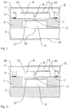
- Fig. 1 is a with two transparent Deckelwafern (top lid wafer 2 on the front of the carrier wafer and bottom cover wafer 3 on the back of the carrier wafer) of borosilicate glass encapsulated volume micromechanically manufactured suspended on torsion springs 11 micromirror 12 shown in cross section, wherein bushings through the carrier wafer. 1 lead from silicon.
- the carrier wafer 1 has been contacted with the lid wafers 2, 3 on both sides by an anodic bonding process.
- the carrier wafer 1 has a frame-shaped, closed planar contact area 7 around the micromirror 12 for contacting with the lid wafers 2, 3.
- a correspondingly dimensioned frame-shaped closed planar contact region 7 is provided in the cover wafers as a mating contact surface.
- the top lid wafer 2 contains depressions 4 which, in conjunction with the carrier wafer 1, form the cavities 5 necessary for the movements of the micromirror.
- the micromirror 12 suspended from torsion springs 11 may, for example, have a diameter of 10 mm.
- the top lid wafer 2 At a maximum tilt of such Micromirror 12 by 10 ° are recesses 4 in the top lid wafer 2 of more than 870 microns necessary, so that the deepest wells 4, measured from the contact areas 7 to the bottom of these wells 4, amount to about 900 microns.
- the bottoms of the deepest recesses 4 at the same time form the areas that act as optical windows 13.
- the depth of the recesses 4 is dimensioned such that the stops to the undeflected torsion springs 11 have a vertical distance between 1 micron and 50 microns.
- the stops 8 have no optical function. They ensure only a mechanically protective functionality of the top lid wafer 2.
- the top lid wafer 2 has three different levels of structure for creating the optical windows 13, the stops 8 and the contact areas 7.
- the optical windows 13 and the planar side of the top lid wafer 2 facing away from the micromirror 12 are provided with an antireflection coating 10 of a layer system of magnesium fluoride and titanium dioxide.
- the bottom lid wafer 3 is not structured and hermetically seals the cavity 5 around the micromirror 12.
- the bottom lid wafer 3 is also provided with antireflection coatings 10 on both sides. This would, for example, offer the possibility of also irradiating the rear side of the micromirror 12 and of using the reflected beam to determine the mirror position.
- Mechanical stops 8 are not present in the bottom lid wafer 3, but can be provided in a further embodiment in order to ensure overload protection in both directions perpendicular to the carrier wafer plane.
- bottom lid wafer 3 does not have optical functionality, a commercially available silicon wafer can be used as in Fig. 2 and Fig. 3 will be shown.
- the bottom lid wafer 3 is provided with a recess 16 in order to enlarge the cavity 5 about the micromirror 12. This is necessary if the micromirror 12, as in the embodiment shown here, has stiffening structures 15 for reducing static and dynamic deformations and / or drive structures 15, for example for vertical drives and / or in wafer thickness.
- the recess 16 in the bottom lid wafer 3 is used to deposit a getter material 14 (eg, zirconium alloys, titanium), which serves to maintain a vacuum within the cavity 5 in the long term.
- a getter material 14 eg, zirconium alloys, titanium
- a further embodiment of the invention provides according to the Fig. 1-3 further recesses 6 in the top lid wafer 2 outside the cavity 5 enclosing the micromirror 12. These recesses 6 enclose the connection pads (pads) 9 of each chip after the connection of carrier wafer 1 and top lid wafer 2.
- buried interconnects under the contact region 7 between carrier wafer 1 and top lid wafer 2 can be led out laterally from the micromirror 12 enclosing cavity 5 to the connection fields 9.
- connection fields 9 can be made accessible without the atmosphere in the cavity 5 enclosing the micromirror 12 to impair. This has the advantage that even before the Separation step, for example, functional tests or measurements on the finished encapsulated micromirror 12 can be performed.
- glass wafers of borosilicate glass are provided, which serve as top 2 and bottom lid wafer 3.
- the glass wafers of borosilicate glass for example, have a thickness between 0.5 mm and 3 mm; depending, among other things, on the required stability.
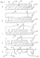
- Fig. 4 shows the sequence of steps for structuring the top lid wafer 2 by means of glass flow method.
- the structures of a forming wafer 21 are molded or transferred onto the top lid wafer 2.
- the basis for the molding wafer 21 is a single-sidedly polished silicon wafer. This molding wafer 21 remains unchanged in the regions through which the optical windows 13 are formed, so that the original surface quality of the polished silicon wafer 21 is retained. In the regions in which the contact regions 7 of the top lid wafer 2 are produced, uniformly deep trenches 23 are etched into the mold wafer 21. The etching depth of these trenches 23 approximately determines the depth of the cavity 5.
- etching processes come into question. Very homogeneously over the entire mold wafer 21, this can be achieved, for example, with time-controlled wet-chemical etching in potassium hydroxide (KOH) or TMAH (tetramethylammonium hydroxide).
- KOH potassium hydroxide
- TMAH tetramethylammonium hydroxide
- plasma assisted dry etching techniques can also produce such trenches 23 with high precision; but usually with the proviso that the width of the trenches 23 is uniform everywhere.
- an SOI wafer silicon on insulator wafer
- the mold wafer 21 instead of the standard silicon wafer, the trenches 23 to etched on the hidden oxide layer.
- the finished structured wafer 21 shows Fig. 4a ,
- the top wafer 2 is anodically bonded to the mold wafer 21, such as 4b shows.
- the mold wafer 21 such as 4b shows.
- the composite of mold wafer 21 and top lid wafer 2 is heated to 600-800 ° C. in an oven.
- the top lid wafer 2 begins to melt and is pressed into the trenches 23, 24 of the forming wafer 21 as a result of the pressure difference between vacuum in the trenches 23, 24 of the forming wafer 21 and the higher ambient pressure in the oven until the trenches 23, 24 of the Formwafers 21 are completely filled with borosilicate glass of the top lid wafer 2.
- the structures of the molding wafer 21 are completely molded onto the top lid wafer 2.
- Fig. 4c Due to the glass flow, the side facing away from the mold wafer 21 of the top lid wafer 2 after cooling is no longer flat ( Fig. 4c ) and must therefore be planarized and smoothed in a precise grinding and polishing process, until finally optical quality is achieved again.
- the result of this step is in Fig. 4d shown.
- the polished top lid wafer 2 is freed from the mold wafer 21 by wet etching away the mold wafer 21.
- the bottom lid wafer 3 is made flat on both sides or with a depression 16 on the side facing the carrier wafer.
- anti-reflection layers 10 of a layer system of magnesium fluoride and titanium oxide are vapor-deposited on the surfaces parallel to the carrier wafer plane after the bonding process of the lid wafers 2, 3, which have an optical function. These antireflection coatings 10 then have to be removed again from the contact regions 7 ( 4e ), since the anti-reflection layers 10 could interfere with the bonding process.
- the removal takes place by means of a polish, which attacks only the contact regions 7, but not the antireflection coatings 10 in the depressions 4, 16.
- the lid wafers 2, 3 are finally bonded to the carrier wafer 1.
Landscapes
- Engineering & Computer Science (AREA)
- Microelectronics & Electronic Packaging (AREA)
- Computer Hardware Design (AREA)
- Physics & Mathematics (AREA)
- Manufacturing & Machinery (AREA)
- General Physics & Mathematics (AREA)
- Optics & Photonics (AREA)
- Micromachines (AREA)
- Mechanical Light Control Or Optical Switches (AREA)
Description
Fertig prozessierte mikromechanische (MEMS) und mikrooptische Systeme (MOEMS) beziehungsweise Bauelemente - wie zum Beispiel Beschleunigungssensoren, Drehratensensoren, Mikrospiegel - bestehen in der Regel aus sehr empfindlichen, zum Teil frei beweglichen Mikrostrukturen (zum Beispiel Balken, Gittern, Platten).Completely processed micro-mechanical (MEMS) and micro-optical systems (MOEMS) or components - such as acceleration sensors, rotation rate sensors, micromirrors - usually consist of very sensitive, partly freely movable microstructures (for example beams, grids, plates).
Während der meisten zur Herstellung benötigten Fertigungsschritte (zum Beispiel Schichtabscheidung, Photo-Lithographie, Ätzverfahren) sind auch die beweglichen Mikrostrukturen noch fest und dadurch unbeweglich mit dem Substrat (Trägersubstrat), üblicherweise einem Wafer (Trägerwafer), verbunden. Erst durch einen sogenannten " Release"-Prozess werden diese Mikrostrukturen frei beweglich. Ab diesem Zeitpunkt sind die beweglichen Mikrostrukturen besonders empfindlich, so dass Verunreinigungen oder mechanische Überbeanspruchungen zur Zerstörung oder Funktionseinschränkung dieser Mikrostrukturen und damit zur Dysfunktion des Bauelements führen können. So kommt beispielsweise bei der Vereinzelung eines Wafers, also dem Zersägen eines Wafers in einzelne Chips, die Waferoberfläche und damit die Mikrostrukturen der MEMS/MOEMS mit Partikeln und Wasser in Berührung. Des Weiteren können die Mikrostrukturen während eines Sägeprozesses relativ starken mechanischen Belastungen ausgesetzt sein.During most of the production steps required for the production (for example, layer deposition, photo lithography, etching method), the movable microstructures are still fixed and thus immovably connected to the substrate (carrier substrate), usually a wafer (carrier wafer). Only through a so-called "release" process, these microstructures are free to move. From this point on, the movable microstructures are particularly sensitive so that contamination or mechanical overstressing can lead to the destruction or functional restriction of these microstructures and thus to the dysfunction of the component. Thus, for example, when a wafer is separated, that is to say the sawing of a wafer into individual chips, the wafer surface and thus the microstructures of the MEMS / MOEMS come into contact with particles and water. Furthermore, the microstructures may be exposed to relatively high mechanical loads during a sawing process.
Um dennoch MEMS/MOEMS mit hoher Ausbeute kostengünstig fertigen zu können, ist man bestrebt, sowohl den "Release"-Prozess als auch Maßnahmen insbesondere zum Schutz der beweglichen Mikrostrukturen bereits durchzuführen, bevor das Substrat vereinzelt beziehungsweise zerteilt wird.Nevertheless, in order to be able to produce MEMS / MOEMS inexpensively with high yield, efforts are being made to carry out both the "release" process and measures, in particular for protecting the movable microstructures, before the substrate is singulated or split.
Die Erfindung betrifft ein Gehäuse zur Verkapselung mikromechanischer und mikrooptischer Bauelemente, welche insbesondere in mobilen Geräten zum Einsatz kommen, und ein Verfahren zur Herstellung eines solchen Gehäuses, wobei sich das Verfahren auch für die Verkapselung der MEMS/MOEMS auf Substrat-Ebene insbesondere auf Wafer-Ebene, d.h. vor dem Vereinzelungsprozess und damit vor der Zerteilung des Substrats, eignet.The invention relates to a housing for encapsulating micromechanical and microoptical components, which are used in particular in mobile devices, and to a method for producing such a housing, the method also being suitable for the encapsulation of the MEMS / MOEMS at the substrate level, in particular on the wafer. Level, ie before the singulation process and thus before the fragmentation of the substrate is suitable.
Gehäuse zur Verkapselung von MEMS/MOEMS sowie Verfahren zu Herstellung solcher Gehäuse insbesondere auf Wafer-Ebene, sogenannte Wafer-Level-Packaging-Verfahren, sind aus der Halbleiterindustrie bekannt.Casing for encapsulation of MEMS / MOEMS and methods for producing such packages, in particular on the wafer level, so-called wafer-level packaging methods, are known in the semiconductor industry.
Wie beispielsweise in der
Sollen die MEMS/MOEMS eine optische Funktion ausüben oder sollen bestimmte Parameter oder physikalische Größen der MEMS/MOEMS optisch gemessen werden - beispielsweise Bestimmung der Auslenkung mittels Interferometer oder durch Auswertung von Videosequenzen - dann bedarf es in der Regel eines optisch transparenten Deckelsubstrats.If the MEMS / MOEMS are to perform an optical function or if certain parameters or physical quantities of the MEMS / MOEMS are to be optically measured - for example determination of the deflection by means of an interferometer or evaluation of video sequences - then an optically transparent cover substrate is generally required.
In der
In der
In der
Aus dem Patent
In der
Der vorliegenden Erfindung liegt die Aufgabe zugrunde, die Nachteile des Standes der Technik zu überwinden und ein Gehäuse zur Verfügung zu stellen, das insbesondere für optische Anwendungen geeignet ist, einen mechanischen Überlastschutz aufweist und auf Substrat- beziehungsweise Wafer-Ebene hergestellt werden kann.The present invention has for its object to overcome the disadvantages of the prior art and to provide a housing that is particularly suitable for optical applications, has a mechanical overload protection and can be produced at the substrate or wafer level.
Gemäß der vorliegenden Erfindung wird die Aufgabe durch ein Gehäuse gemäß Anspruch 1 gelöst. Anspruch 6 gibt ein Verfahren zur Herstellung des erfindungsgemäßen Gehäuses an.According to the present invention, the object is achieved by a housing according to
Die Unteransprüche lehren vorteilhafte Weiterbildungen;The subclaims teach advantageous developments;
Das erfindungsgemäße Gehäuse dient der Verkapselung von einem oder mehreren mikromechanischen und/oder mikrooptischen Bauelement/en und weist ein Trägersubstrat, mit mindestens einem mikromechanischen und/oder mikrooptischen Bauelement, und mindestens ein Deckelsubstrat auf. Das Trägersubstrat und das Deckelsubstrat stehen miteinander in Verbindung, bevorzugt stoffschlüssig in Verbindung, und bilden einen oder mehrere Hohlräume, der/die das mindestens eine mikromechanische und/oder mikrooptische Bauelement zumindest teilweise einschließt. Die dem mindestens einen mikromechanischen und/oder mikrooptischen Bauelement zugewandte Seite des Deckelsubstrats weist mindestens ein optisches Fenster und mindestens einen mechanischen Anschlag auf.The housing according to the invention serves for the encapsulation of one or more micromechanical and / or microoptical component (s) and has Carrier substrate, with at least one micromechanical and / or micro-optical device, and at least one lid substrate. The carrier substrate and the lid substrate are connected to each other, preferably cohesively in connection, and form one or more cavities, which at least partially encloses the at least one micromechanical and / or micro-optical component. The side of the cover substrate facing the at least one micromechanical and / or microoptical component has at least one optical window and at least one mechanical stop.
Ein Gehäuse zur Verkapselung von MEMS/MOEMS, insbesondere beweglichen MEMS/MOEMS, soll in der Regel mindestens einen Schutz gegen Verunreinigungen bieten und gleichzeitig die mechanische und/oder optische Funktionalität der MEMS/MOEMS nicht beeinträchtigen. Als Gehäuse kann beispielsweise ein Deckelsubstrat fungieren, das mit dem Trägersubstrat in Verbindung steht. Sollte die Funktionalität der MEMS/MOEMS nicht nur auf Bewegungen in der beziehungsweise parallel zur Trägersubstratebene beschränkt sein, sondern auch Bewegungen senkrecht zur Trägersubstratebene vorsehen, muss das Gehäuse den MEMS/MOEMS entsprechende Bewegungsfreiheit gewährleisten.A housing for encapsulating MEMS / MOEMS, in particular movable MEMS / MOEMS, should as a rule provide at least protection against contaminants, while at the same time not impairing the mechanical and / or optical functionality of the MEMS / MOEMS. As a housing, for example, a lid substrate can act, which is in communication with the carrier substrate. Should the functionality of the MEMS / MOEMS not only be limited to movements in or parallel to the carrier substrate plane, but also provide movements perpendicular to the carrier substrate plane, the housing must ensure the MEMS / MOEMS appropriate freedom of movement.
So kann das Deckelsubstrat beispielsweise Vertiefungen aufweisen, die in Verbindung mit dem Trägersubstrat Hohlräume um die MEMS/MOEMS bilden, so dass die Funktionalität der MEMS/MOEMS nicht eingeschränkt wird.For example, the lid substrate may have recesses which in combination with the carrier substrate form cavities around the MEMS / MOEMS, so that the functionality of the MEMS / MOEMS is not restricted.
Um auch sehr vibrations- und schockempfindliche MEMS/MOEMS mit weichen Aufhängungen und niedrigen Resonanzfrequenzen mit hoher Ausbeute fertigen zu können, bedarf es Anschlägen, die die MEMS/MOEMS vor mechanischer Überlast (zum Beispiel Schock, Vibrationen, usw.), wie sie beispielsweise bei mobilen Anwendungen (zum Beispiel in Mobiltelefonen) auftreten kann, schützen.In order to be able to fabricate very vibration- and shock-sensitive MEMS / MOEMS with soft suspensions and low resonance frequencies with high yield, it is necessary to provide stops which prevent the MEMS / MOEMS from being subjected to mechanical overload (for example) Shock, vibration, etc.) such as may occur in mobile applications (for example in mobile phones).
Während laterale Kräfte, die in der Substratebene wirken, durch laterale Anschläge im MEMS/MOEMS-Design vorgesehen und entsprechend realisiert werden können, bedarf es für senkrecht aus der Substratebene wirkende Kräfte zusätzlicher vertikaler Anschläge.While lateral forces acting in the substrate plane can be provided by lateral stops in the MEMS / MOEMS design and can be realized accordingly, forces acting vertically from the substrate plane require additional vertical stops.
Das erfindungsgemäße Gehäuse weist einen oder mehrere integrierte mechanische Anschläge auf, der/die bevorzugt an einer beliebigen Stelle aus dem Deckelsubstrat in Richtung der MEMS/MOEMS ragt/ragen.The housing according to the invention has one or more integrated mechanical stops, which preferably project from the cover substrate in any direction in the direction of the MEMS / MOEMS.
Durch ein Herausragen der Anschläge insbesondere aus der den MEMS/MOEMS zugewandten Fläche der optischen Fenster kann verhindert werden, dass Bereiche der MEMS/MOEMS mit den größten Auslenkungsamplituden - und damit zum Beispiel bei Rotationsbewegungen mit der höchsten Geschwindigkeit - am Deckelsubstrat anstoßen. In Verbindung mit der freien Wahl der Position der Anschläge besteht die Möglichkeit, dass man Bereiche der MEMS/MOEMS für den Kontakt mit den Anschlägen vorsieht, die am besten dafür geeignet sind; zum Beispiel weil deren maximale vertikale Geschwindigkeit im Vergleich zu anderen Bereichen gering ist, sie keine aktive Funktion ausüben beziehungsweise keine aktiven Bereiche darstellen und/oder diese Bereiche mechanisch besonders stabil ausgelegt sind.By protruding the stops, in particular from the surface of the optical windows facing the MEMS / MOEMS, it is possible to prevent areas of the MEMS / MOEMS having the greatest deflection amplitudes - and thus for example during rotational movements with the highest speed - from abutting the cover substrate. In connection with the free choice of the position of the stops, there is the possibility of providing areas of the MEMS / MOEMS for contact with the stops which are best suited for this purpose; For example, because their maximum vertical speed is low compared to other areas, they do not perform an active function or represent no active areas and / or these areas are designed mechanically very stable.
Damit lässt sich das Risiko einer Beschädigung der Mikrostrukturen und damit der MEMS/MOEMS bei mechanischen Überbeanspruchungen reduzieren.This reduces the risk of damage to the microstructures and thus of the MEMS / MOEMS in the event of mechanical overstress.
Prinzipiell sollten die mechanischen Anschläge die Funktionalität beziehungsweise den gewünschten Arbeitsbereich der MEMS/MOEMS nicht einschränken, wobei der Abstand der mechanischen Anschläge zu den für den Kontakt mit den Anschlägen vorgesehenen Bereichen der MEMS/MOEMS bevorzugt möglichst gering sein sollte.In principle, the mechanical stops should not restrict the functionality or the desired working range of the MEMS / MOEMS, whereby the distance between the mechanical stops and the areas of the MEMS / MOEMS intended for contact with the stops should preferably be as small as possible.
Bei manchen Anwendungen hat das Gehäuse auch optische Funktionen zu erfüllen. Das erfindungsgemäße Gehäuse bietet durch die herausragenden Anschläge den Vorteil, dass es bei mechanischen Überbeanspruchungen nur zum Kontakt der MEMS/MOEMS mit den Anschlägen kommt. Andere Bereiche des Deckelsubstrats kommen nicht mit den MEMS/MOEMS in Berührung. Dadurch werden die anderen Bereiche des Deckelsubstrats, die beispielsweise als optische Fenster fungieren, nicht beschädigt oder in ihrer Funktionalität beeinträchtigt.In some applications, the housing also has to perform optical functions. Due to the outstanding stops, the housing according to the invention offers the advantage that, in the case of mechanical overstresses, only the MEMS / MOEMS contacts the stops. Other areas of the lid substrate do not come into contact with the MEMS / MOEMS. As a result, the other areas of the cover substrate, which act as optical windows, for example, are not damaged or impaired in their functionality.
Unter einem optischen Fenster wird erfindungsgemäß ein Bereich des Gehäuses verstanden, der für beliebige Wellenlängen und/oder Wellenlängenbereiche elektromagnetischer Strahlung - insbesondere die durch das zu verkapselnde MEMS/MOEMS zu verarbeitende Strahlung und damit die in der Anwendung eingesetzte Strahlung - aus dem infraroten, sichtbaren (Licht) und ultravioletten Frequenzbereich durchlässig, insbesondere transparent, ist und zudem üblicherweise hohe Qualitätsanforderungen insbesondere an die Oberflächenrauhigkeit, die Ebenheit und die Planparallelität erfüllt. Des Weiteren sollten diese Bereiche vorzugsweise eine homogene Materialstruktur aufweisen.According to the invention, an optical window is understood as meaning an area of the housing which, for any wavelengths and / or wavelength ranges of electromagnetic radiation-in particular the radiation to be processed by the MEMS / MOEMS to be encapsulated and thus the radiation used in the application-from the infrared, visible (FIG. Light) and ultraviolet frequency range permeable, especially transparent, and also usually high quality requirements in particular to the surface roughness, the flatness and the plane parallelism. Furthermore, these regions should preferably have a homogeneous material structure.
Ein typisches mikrooptisches Bauelement ist der Mikrospiegel, der zum Beispiel in der Video-Laser-Projektion als Scanspiegel eingesetzt werden kann, um einen einfallenden Laserstrahl abzulenken. Dabei soll der Laserstrahl durch das Gehäuse möglichst wenig gestreut und deformiert werden.A typical micro-optical device is the micromirror, which can be used in the video laser projection as a scanning mirror, for example, to deflect an incident laser beam. In this case, the laser beam should be scattered and deformed by the housing as little as possible.
Zur Erzeugung der Hohlräume zwischen Trägersubstrat und Deckelsubstrat wird beispielsweise das Deckelsubstrat mit Vertiefungen versehen, so dass Trägersubstrat und Deckelsubstrat nach ihrer Verbindung die MEMS/MOEMS in der Regel komplett umschließen. Bei den meisten Anwendungen sind Tiefen zwischen etwa 50 µm und 900 µm für die Vertiefungen ausreichend. Um auch größeren MEMS/MOEMS ausreichend Auslenkungsfreiheit gewähren zu können, sind Vertiefungen im Deckelsubstrat tiefer 900 µm von Vorteil.To produce the cavities between the carrier substrate and the lid substrate, for example, the lid substrate is provided with depressions, so that the carrier substrate and lid substrate generally completely surround the MEMS / MOEMS after their connection. In most applications, depths are between about 50 μm and 900 μm is sufficient for the wells. In order to be able to provide sufficient freedom of deflection even for larger MEMS / MOEMS, recesses in the cover substrate lower 900 μm are advantageous.
Solche Vertiefungen sind beispielsweise für relativ große beweglich aufgehängte Mikrospiegel zweckmäßig, die einen Durchmesser von 10 mm haben können. Ein Verkippen eines so dimensionierten Mikrospiegels um 10° um seine Mittelachse führt zu einer maximalen aus der Substratebene gerichteten Auslenkung von fast 870 µm.Such depressions are useful, for example, for relatively large movably suspended micromirrors, which may have a diameter of 10 mm. Tilting of such a dimensioned micromirror by 10 ° about its central axis leads to a maximum directed from the substrate plane deflection of almost 870 microns.
Besonders vorteilhaft ist es, wenn das Gehäuse die MEMS/MOEMS hermetisch dicht von der Umgebung abschließt, so dass im Gehäuse eine bestimmte Atmosphäre einstellbar ist. Dadurch ist ein besonders guter Schutz gegen Verunreinigungen gegeben, wodurch die Gefahr einer Dysfunktion des verkapselten MEMS/MOEMS minimiert wird. Zudem lässt sich in den Hohlräumen eine von der Umgebung unabhängige Atmosphäre einstellen.It is particularly advantageous if the housing terminates the MEMS / MOEMS hermetically sealed from the environment so that a certain atmosphere can be set in the housing. This provides a particularly good protection against impurities, which minimizes the risk of dysfunction of the encapsulated MEMS / MOEMS. In addition, an atmosphere independent of the environment can be set in the cavities.
Während bei oberflächenmikromechanisch gefertigten MEMS/MOEMS eine hermetisch dichte Verkapselung bereits durch einen Verbund aus Trägersubstrat und einem Deckelsubstrat erreicht werden kann, bedarf es bei volumenmikromechanisch gefertigten MEMS/MOEMS, welche zum Teil vollständig durch das Trägersubstrat hindurch geätzte Mikrostrukturen besitzen, mindestens eines zweiten Deckelsubstrats, das mit der der ersten Seite des Trägersubstrats, die mit dem ersten Deckelsubstrat in Verbindung steht, gegenüberliegenden zweiten Seite des Trägersubstrats verbunden wird, so dass das Trägersubstrat beidseitig mit Deckelsubstraten versehen ist.While a hermetically sealed encapsulation can already be achieved in the case of surface-micromechanically fabricated MEMS / MOEMS by a composite of carrier substrate and a lid substrate, at least one second lid substrate is required for volume micromechanically fabricated MEMS / MOEMS, which partially have microstructures completely etched through the carrier substrate. which is connected to the second side of the carrier substrate opposite the first side of the carrier substrate, which is in communication with the first lid substrate, so that the carrier substrate is provided on both sides with lid substrates.
In vielen Anwendungsfällen wird ein Gehäuseinnendruck unterhalb des atmosphärischen Luftdrucks bevorzugt. Für MEMS/MOEMS besonders bevorzugt wird ein Gehäuseinnendruck von etwa 10-3 mbar bis etwa 1 mbar. Dadurch lässt sich beispielsweise die Dämpfung insbesondere bei Systemen, die bei Resonanz betrieben werden, reduzieren und dadurch höhere Gütefaktoren und größere Auslenkungsamplituden erzielen.In many applications, a housing internal pressure below the atmospheric air pressure is preferred. Particularly preferred for MEMS / MOEMS is a housing internal pressure of about 10 -3 mbar to about 1 mbar. This can be done For example, reduce the attenuation, especially in systems that are operated at resonance, and thereby achieve higher quality factors and larger displacement amplitudes.
Bei anderen Anwendungen ist es vorteilhaft, wenn die Hohlräume mit einem Gas gefüllt sind, um dadurch bestimmte Eigenschaften der MEMS/MOEMS gezielt zu beeinflussen. Dabei kommen Gase in Frage, die trocken und nicht elektrisch leitfähig sind, mit den für das Gehäuse und die MEMS/MOEMS verwendeten Materialien chemisch nicht reagieren und die erforderliche Transparenz aufweisen; als Beispiele seien Inertgase wie Edelgase, Stickstoff oder SF6 genannt.In other applications, it is advantageous if the cavities are filled with a gas in order thereby to influence certain properties of the MEMS / MOEMS in a targeted manner. In this case, gases that are dry and not electrically conductive, do not react chemically with the materials used for the housing and the MEMS / MOEMS and have the required transparency; Examples include inert gases such as noble gases, nitrogen or SF 6 .
So wird beispielsweise bei Anwendungen, bei denen Wärme möglichst schnell an das Gehäuse und die Umgebung abgeleitet werden soll, Argon als Gehäuseatmosphärengas eingesetzt, da Argon elektrisch nicht leitfähig ist, trotzdem aber eine relativ hohe thermische Leitfähigkeit besitzt. Zudem ist die Diffusionsneigung von Argon so gering, dass langzeitstabile Druckverhältnisse im Gehäuse möglich sind.Thus, for example, in applications where heat is to be dissipated as quickly as possible to the housing and the environment, argon is used as a housing atmosphere gas, since argon is electrically non-conductive, but still has a relatively high thermal conductivity. In addition, the diffusion tendency of argon is so low that long-term stable pressure conditions in the housing are possible.
Als Trägersubstrat werden bevorzugt Siliziumwafer verwendet, da die Prozesse der Siliziumtechnologie ausgereift sind und gut beherrscht werden.The carrier substrate used is preferably silicon wafer, since the processes of silicon technology are mature and well controlled.
Insbesondere für bewegliche MEMS/MOEMS, die bei optischen Anwendungen zum Einsatz kommen, ist ein Gehäuse notwendig, das zumindest in Teilbereichen den oben genannten Anforderungen an ein optisches Fenster entspricht sowie neben der mechanischen auch die optische Funktionalität des gekapselten MEMS/MOEMS möglichst nicht beziehungsweise wenig beeinträchtigt.In particular, for movable MEMS / MOEMS, which are used in optical applications, a housing is necessary, which at least partially corresponds to the above-mentioned requirements for an optical window as well as mechanical as well as the optical functionality of the encapsulated MEMS / MOEMS as little as possible or not impaired.
Daher ist es von Vorteil, wenn sich die thermischen Ausdehnungskoeffizienten von Trägersubstrat und Deckelsubstrat möglichst gering unterscheiden oder zwischen den beiden Substraten eine Schicht angeordnet ist, mit der die unterschiedlichen Ausdehnungskoeffizienten ausgeglichen werden können.It is therefore advantageous if the coefficients of thermal expansion of the carrier substrate and the lid substrate differ as little as possible or between the thermal expansion coefficients two substrates, a layer is arranged, with which the different expansion coefficients can be compensated.
Dadurch lassen sich thermisch induzierte mechanische Spannungen zwischen Trägersubstrat und Deckelsubstrat minimieren und die Gefahr von Schädigungen am Gehäuse und den gekapselten MEMS/MOEMS reduzieren.As a result, thermally induced mechanical stresses between the carrier substrate and lid substrate can be minimized and the risk of damage to the housing and the encapsulated MEMS / MOEMS can be reduced.
Das Deckelsubstrat enthält oder besteht bevorzugt aus Glas und/oder einem glasähnlichen Material. Unter glasähnlichen Materialien werden erfindungsgemäß Stoffe verstanden, die wegen ihrer thermodynamischen Eigenschaften (amorpher Aufbau, Glasübergangstemperatur) Gläsern ähneln, obwohl sich ihre chemische Zusammensetzung von der der Silikatgläser unterscheidet. Als Beispiele seien hier die in der Chemie bekannten Kunstgläser oder organischen Vitroide wie Polymethylmethacrylate (PMMA), Polycarbonat und Polystyrol genannt.The lidding substrate preferably contains or consists of glass and / or a glass-like material. Under glass-like materials materials according to the invention are understood to be similar because of their thermodynamic properties (amorphous structure, glass transition temperature) glasses, although their chemical composition is different from that of silicate glasses. Examples include the art glass known in the art or organic Vitroide such as polymethylmethacrylate (PMMA), polycarbonate and polystyrene.
Besonders geeignete Gläser sind Silikatgläser, insbesondere Borsilikatgläser, da Borsilikatgläser sehr chemikalien- und temperaturbeständig sind. Die Temperaturbeständigkeit und Unempfindlichkeit der Borsilikatgläser gegen plötzliche Temperaturschwankungen sind eine Folge ihres geringen Wärmeausdehnungskoeffizienten. Zudem ist der Transmissionsgrad insbesondere im sichtbaren Bereich mit über 90% sehr hoch.Particularly suitable glasses are silicate glasses, in particular borosilicate glasses, since borosilicate glasses are very resistant to chemicals and to high temperatures. The temperature resistance and insensitivity of the borosilicate glasses against sudden temperature fluctuations are a consequence of their low coefficient of thermal expansion. In addition, the transmittance is very high, especially in the visible range with over 90%.
Um optischen Qualitätsansprüchen gerecht zu werden, sollten die optischen Fenster des Gehäuses eine Ebenheits- und/oder Planparallelitätsabweichung kleiner einem Viertel der Wellenlänge der bei der Anwendung eingesetzten elektromagnetischen Strahlung aufweisen, wobei üblicherweise Wellenlängen vom ultravioletten bis in den infraroten Wellenlängenbereich (zum Beispiel zwischen etwa 200 nm und etwa 15 µm) Anwendung finden. Demzufolge sind bei längerwelligem Licht mit Wellenlängen unter 720 nm Werte für die Ebenheits- und/oder Planparallelitätsabweichung kleiner 180 nm von Vorteil. Bei Verwendung von kürzerwelligem Licht mit Wellenlängen unter 440 nm steigen die Anforderungen an die optischen Fenster, so dass Werte für die Ebenheits- und/oder Planparallelitätsabweichung kleiner 110 nm bevorzugt werden.To meet optical quality requirements, the optical windows of the housing should have a flatness and / or parallelism deviation less than one quarter of the wavelength of the electromagnetic radiation used in the application, usually wavelengths from the ultraviolet to the infrared wavelength range (for example, between about 200 nm and about 15 μm) find application. Consequently, with longer wavelength light with wavelengths below 720 nm values for the evenness and / or plane parallelism deviation of less than 180 nm are advantageous. When using shorter wavelength light with wavelengths below 440 nm, the demands on the optical windows increase, so that values for the evenness and / or parallelism deviation of less than 110 nm are preferred.
Optische Fenster, die diese Anforderungen erfüllen, verursachen geringere Abweichungen und eine geringere Strahlaufweitung des optischen Strahlenverlaufs, was zu einer geringeren Verfälschung der optischen Signale führt.Optical windows that meet these requirements cause smaller deviations and less beam expansion of the optical beam path, resulting in less distortion of the optical signals.
Zudem sollte die quadratische Oberflächenrauhigkeit der optischen Fenster möglichst gering sein, bevorzugt kleiner 15 nm, besonders bevorzugt kleiner 5 nm. Dadurch lässt sich insbesondere die durch das Deckelsubstrat verursachte Streuung reduzieren.In addition, the square surface roughness of the optical window should be as low as possible, preferably less than 15 nm, particularly preferably less than 5 nm. This makes it possible in particular to reduce the scattering caused by the cover substrate.
Die Werte für die Ebenheits- und Planparallelitätsabweichung sowie für die quadratische Oberflächenrauhigkeit wurden mittels interferometrischer Messmethode bestimmt. Für die Messungen wurde das Weißlicht- und Phaseninterferometer MicroMap 512 der Firma Atos verwendet.The values for the evenness and planarity deviation as well as for the quadratic surface roughness were determined by means of an interferometric measuring method. For the measurements, the white light and phase interferometer MicroMap 512 from Atos was used.
Um die Eigenschaften der optischen Fenster zusätzlich zu optimieren, ist es von Vorteil, diese Bereiche zumindest teilweise mit Veredlungsschichten zu versehen.In order to additionally optimize the properties of the optical windows, it is advantageous to provide these areas at least partially with finishing layers.
Besonders häufig eingesetzte Veredlungsschichten sind beispielsweise Entspiegelungsschichten, die Reflexionen an den optischen Fenstern und damit Strahlungsverluste verringern. Solche Entspiegelungsschichten lassen sich zum Beispiel durch Schichtsysteme aus Magnesiumfluorid und Titanoxid oder Siliziumdioxid und Titandioxid realisieren.Particularly used finishing layers are, for example, anti-reflection layers, which reduce reflections on the optical windows and thus radiation losses. Such antireflection coatings can be realized, for example, by layer systems of magnesium fluoride and titanium oxide or silicon dioxide and titanium dioxide.
Des Weiteren finden Antistatik-Schichten, die ein elektrisches Aufladen des Deckelsubstrats minimieren, häufig Verwendung. Ein für Antistatik-Schichten in optischen Anwendungen besonders geeignetes Material ist ITO (Indiumzinnoxid), da es dotiert eine hohe elektrische Leitfähigkeit aufweist und über einen breiten Frequenzbereich eine hohe Transparenz aufweist.Furthermore, antistatic layers that minimize electrical charging of the cap substrate are often used. One for antistatic layers in Particularly suitable material for optical applications is ITO (indium tin oxide), since it has a high electrical conductivity and has a high transparency over a wide frequency range.
Weiterhin können Reflexionsschichten, zum Beispiel Metallschichten, aufgebracht werden, die nach Strukturierung lokal reflektierende Bereiche bilden, zum Beispiel um einen einfallenden Lichtstrahl räumlich zu begrenzen (Blendenfunktion) oder um in Nachbarschaft zu den optischen Fenstern einen statischen Umlenkspiegel zu bilden. Bevorzugt eingesetzte Veredlungsschichten sind des Weiteren Absorberschichten, die elektromagnetische Strahlung bestimmter Wellenlängen oder ganzer Wellenlängenbereiche absorbieren.Furthermore, reflection layers, for example metal layers, can be applied, which after structuring form locally reflecting areas, for example to spatially limit an incident light beam (aperture function) or to form a static deflection mirror in the vicinity of the optical windows. Preferred finishing layers are furthermore absorber layers which absorb electromagnetic radiation of specific wavelengths or entire wavelength ranges.
Das erfindungsgemäße Verfahren zur Herstellung eines Gehäuses zur Verkapselung mikromechanischer und/oder mikrooptischer Bauelemente weist die folgenden Schritte auf:
- Bereitstellen eines Trägersubstrats mit mindestens einem mikromechanischen und/oder mikrooptischen Bauelement
- Bereitstellen mindestens eines Deckelsubstrats, das mindestens ein optisches Fenster und mindestens einen mechanischen Anschlag aufweist
- Verbinden des Trägersubstrats mit dem mindestens einen Deckelsubstrat derart, dass das Trägersubstrat und das mindestens eine Deckelsubstrat mindestens einen Hohlraum bilden, der das mindestens eine mikromechanische und/oder mikrooptische Bauelement zumindest teilweise einschließt.
- Provision of a carrier substrate with at least one micromechanical and / or micro-optical component
- Providing at least one lid substrate having at least one optical window and at least one mechanical stop
- Connecting the carrier substrate with the at least one lid substrate such that the carrier substrate and the at least one lid substrate form at least one cavity which at least partially encloses the at least one micromechanical and / or micro-optical component.
Das erfindungsgemäße Verfahren dient der Verkapselung von MEMS/MOEMS, die üblicherweise auf einem Trägersubstrat aufgebracht oder angeordnet sind. Üblicherweise findet als Trägersubstrat ein Siliziumwafer Anwendung, auf dem durch oberflächenmikromechanische oder volumenmikromechanische Prozesse die zu verkapselnden MEMS/MOEMS erzeugt werden.The method according to the invention serves for the encapsulation of MEMS / MOEMS, which are usually applied or arranged on a carrier substrate. Usually, a silicon wafer is used as the carrier substrate on which the MEMS / MOEMS to be encapsulated are produced by surface micromechanical or volume micromechanical processes.
Für die Verkapselung ist des Weiteren ein Deckelsubstrat erforderlich, welches üblicherweise bereits vor der Erzeugung der optischen Fenster und der mechanischen Anschläge zumindest in Teilbereichen, im Regelfall in seiner Gesamtheit, für die in der Anwendung eingesetzte elektromagnetische Strahlung durchlässig ist. Bei den meisten optischen Anwendungen wird allerdings eine möglichst hohe Transparenz dieser für die in der Anwendung eingesetzte elektromagnetische Strahlung durchlässigen Bereiche gefordert, damit beispielsweise ein Laserstrahl möglichst unbeeinflusst das MEMS/MOEMS erreicht.Furthermore, a cover substrate is required for the encapsulation, which is usually permeable to the electromagnetic radiation used in the application at least in some areas, generally in its entirety, even before the optical windows and the mechanical stops are produced. In most optical applications, however, the highest possible transparency of these areas permeable to the electromagnetic radiation used in the application is required, so that, for example, a laser beam reaches the MEMS / MOEMS as uninfluenced as possible.
Auch um diesen Ansprüchen gerecht zu werden, wird das Deckelsubstrat üblicherweise strukturiert. Hierbei werden Vertiefungen für die Hohlräume, die optischen Fenster und die mechanischen Anschläge erzeugt.In order to meet these requirements, the lid substrate is usually structured. This cavities for the cavities, the optical windows and the mechanical stops are generated.
Als Deckelsubstrat eignen sich - wie vorstehend erläutert - verschiedene Gläser sowie bestimmte glasähnliche Kunststoffe. Verschiedene in der Siliziumtechnologie verwendete Strukturierungsverfahren lassen sich auch für Glassubstrate nutzen. So könnten beispielsweise die Vertiefungen mit HF-Lösung geätzt werden. Allerdings führt naßchemisches strukturiertes Ätzen von Glassubstraten in der Regel zu beträchtlichen Inhomogenitäten bezüglich der Ätztiefe innerhalb der geätzten Flächen (ungenügende Planparallelität der Flächen) und darüber hinaus zu stark angerauten Oberflächen, und zwar umso stärker je tiefer geätzt wird. In der Regel ist ein so strukturiertes Deckelsubstrat für optische Einsatzzwecke ungeeignet.As the cover substrate are - as explained above - different glasses and certain glass-like plastics. Various structuring methods used in silicon technology can also be used for glass substrates. For example, the wells could be etched with HF solution. However, wet-chemical structured etching of glass substrates usually leads to considerable inhomogeneities with regard to the etching depth within the etched surfaces (insufficient plane parallelism of the surfaces) and moreover to strongly roughened surfaces, and although the more deeply etched the deeper. As a rule, such a structured cover substrate is unsuitable for optical applications.
Um qualitativ hochwertige optische Oberflächen zu erhalten, eignet sich zur Strukturierung des Deckelsubstrats beispielsweise ein Glasfließ-Verfahren, bei dem die Strukturen eines Formsubstrats beispielsweise auf ein Glassubstrat abgeformt werden. Dabei wird die Oberflächenqualität des Glassubstrats hauptsächlich durch die Oberflächenqualität des Formsubstrats bestimmt.In order to obtain high-quality optical surfaces, it is possible, for example, to pattern the cover substrate using a glass flow method, in which the structures of a molding substrate are shaped, for example, onto a glass substrate. At this time, the surface quality of the glass substrate is mainly determined by the surface quality of the molding substrate.
In einer vorteilhaften Ausgestaltung werden nach dem Strukturieren des Deckelsubstrats insbesondere die optischen Fenster zumindest teilweise mit einer Entspiegelungsschicht und/oder einer Antistatik-Schicht und/oder einer Reflexionsschicht und/oder einer Absorberschicht versehen, wodurch sich die optische Funktionalität des Gehäuses verbessern lässt.In an advantageous embodiment, after the structuring of the cover substrate, in particular the optical windows are at least partially provided with an antireflection coating and / or an antistatic layer and / or a reflection layer and / or an absorber layer, whereby the optical functionality of the housing can be improved.
In einem weiteren Verfahrensschritt werden das Trägersubstrat und das mindestens eine Deckelsubstrat miteinander verbunden, so dass das Trägersubstrat und das mindestens eine Deckelsubstrat mindestens einen Hohlraum bilden, der das MEMS/MOEMS zumindest teilweise einschließt.In a further method step, the carrier substrate and the at least one lid substrate are connected to one another so that the carrier substrate and the at least one lid substrate form at least one cavity that at least partially encloses the MEMS / MOEMS.
Dafür sind generell alle zweckmäßigen Verbindungstechniken einsetzbar wie zum Beispiel Kleben, Löten oder Bonden.For this purpose, generally all suitable joining techniques can be used, such as gluing, soldering or bonding.
In einer bevorzugten Ausgestaltung werden das Trägersubstrat und das mindestens eine Deckelsubstrat durch anodisches und/oder eutektisches Bonden und/oder Glasfritt-Bonden miteinander verbunden. Vor allem in der Halbleiterindustrie sind diese Bondverfahren häufig eingesetzte Verbindungstechniken insbesondere zur hermetisch dichten Verkapselung von Bauelementen.In a preferred embodiment, the carrier substrate and the at least one lid substrate are connected to one another by anodic and / or eutectic bonding and / or glass frit bonding. Especially in the semiconductor industry, these bonding methods are frequently used bonding techniques, in particular for the hermetically sealed encapsulation of components.
Eutektisches Bonden wird besonders bevorzugt, wenn von den MEMS/MOEMS absorbierte Energie, zum Beispiel Strahlungsenergie, auf das Deckelsubstrat abgeführt werden soll.Eutectic bonding is particularly preferred when energy absorbed by the MEMS / MOEMS, for example radiant energy, is to be dissipated onto the lid substrate.
Je nachdem in welcher Umgebung der Bondprozess des Deckelsubstrats beziehungsweise der Deckelsubstrate durchgeführt wird, kann eine ganz bestimmte Atmosphäre - zum Beispiel ein Druck unterhalb des atmosphärischen Luftdrucks, besonders bevorzugt zwischen etwa 10-3 mbar und etwa 1 mbar, und/oder eine Inertgas-Füllung, zum Beispiel mit Argon - in einem hermetisch dichten Gehäuse erzeugt werden. Es werden daher bevorzugt Verbindungstechniken gewählt, die eine stabile Atmosphäre im Gehäuse gewährleisten können.Depending on the environment in which the bonding process of the cover substrate or the cover substrates is carried out, a very specific atmosphere - for example, a pressure below the atmospheric air pressure, more preferably between about 10 -3 mbar and about 1 mbar, and / or an inert gas filling , for example, with argon - be produced in a hermetically sealed housing. It is therefore preferred to choose bonding techniques that can ensure a stable atmosphere in the housing.
Das erfindungsgemäße Verfahren ist besonders bevorzugt auf Wafer-Ebene als Wafer-Level-Packaging-Verfahren einsetzbar, wodurch sich mehrere MEMS/MOEMS gleichzeitig verkapseln lassen und damit ein zeitsparendes und effektives Verkapselungsverfahren gegeben ist.The method according to the invention is particularly preferably usable at wafer level as a wafer-level packaging method, whereby several MEMS / MOEMS can be encapsulated simultaneously and thus a time-saving and effective encapsulation method is provided.
Bevorzugt wird das Verfahren zur Verkapselung von beweglichen Mikrospiegeln und/oder Mikrospiegel-Arrays eingesetzt.The method is preferably used for the encapsulation of movable micromirrors and / or micromirror arrays.
Ohne Einschränkung der Allgemeinheit wird die Erfindung anhand schematischer Zeichnungen und eines Ausführungsbeispiels nachfolgend näher beschrieben.
-
Fig. 1 zeigt ein mit zwei transparenten Deckelwafern 2, 3 verkapselten volumenmikromechanisch gefertigten Mikrospiegel 12, der anTorsionsfedern 11 aufgehängt ist. -
Fig. 2 zeigt ein mit einem transparenten 2 und einem nicht transparenten ebenen Deckelwafer 3 verkapselten volumenmikromechanisch gefertigten Mikrospiegel 12, der anTorsionsfedern 11 aufgehängt ist. -
Fig. 3 zeigt ein mit einem transparenten 2 und einem nicht transparenten, mit einer Vertiefung versehenen Deckelwafer 3 verkapselten volumenmikromechanisch gefertigten Mikrospiegel 12, der anTorsionsfedern 11 aufgehängt ist. -
Fig. 4 zeigt die Schrittfolge zur Herstellung eines Deckelwafers 2 mittels Glasfließ-Verfahren.
-
Fig. 1 shows a with twotransparent Deckelwafern volume micro-mechanically micromirror 12, which is suspended from torsion springs 11. -
Fig. 2 shows a volume micromechanically manufacturedmicromirror 12 which is encapsulated with torsion springs 11 and is encapsulated with a transparent 2 and a non-transparentflat lid wafer 3. -
Fig. 3 shows a with a transparent 2 and a non-transparent, provided with arecess lid wafer 3 encapsulatedvolume micromachined micromirror 12, which is suspended from torsion springs 11. -
Fig. 4 shows the sequence of steps for producing alid wafer 2 by means of glass flow method.
In
Zudem weist der Trägerwafer 1 für die Kontaktierung mit den Deckelwafern 2, 3 einen rahmenförmigen geschlossenen planaren Kontaktbereich 7 um den Mikrospiegel 12 herum auf. Ein entsprechend dimensionierter rahmenförmiger geschlossener planarer Kontaktbereich 7 ist bei den Deckelwafern als Gegenkontaktfläche vorgesehen.In addition, the
Der Top-Deckelwafer 2 enthält Vertiefungen 4, die in Verbindung mit dem Trägerwafer 1 die für die Bewegungen des Mikrospiegels notwendigen Hohlräume 5 bilden.The
Der an Torsionsfedern 11 aufgehängte Mikrospiegel 12 kann zum Beispiel einen Durchmesser von 10 mm haben. Bei einer maximalen Verkippung eines derartigen Mikrospiegels 12 um 10° sind Vertiefungen 4 im Top-Deckelwafer 2 von über 870 µm notwendig, so dass die tiefsten Vertiefungen 4, gemessen von den Kontaktbereichen 7 bis zum Boden dieser Vertiefungen 4, etwa 900 µm betragen. Die Böden der tiefsten Vertiefungen 4 bilden gleichzeitig die Bereiche, die als optische Fenster 13 fungieren. Für die mechanischen Anschläge 8 ist die Tiefe der Vertiefungen 4 so dimensioniert, dass die Anschläge zu den nicht ausgelenkten Torsionsfedern 11 einen vertikalen Abstand zwischen 1 µm und 50 µm aufweisen. Die Anschläge 8 haben keine optische Funktion. Sie gewährleisten nur eine mechanisch protektive Funktionalität des Topdeckel-Wafers 2. In der Ausführungsform nach
Die optischen Fenster 13 sowie die planare dem Mikrospiegel 12 abgewandte Seite des Top-Deckelwafers 2 sind mit einer Entspiegelungsschicht 10 aus einem Schichtsystem aus Magnesiumfluorid und Titandioxid versehen.The
Der Bottom-Deckelwafer 3 ist nicht strukturiert ausgeführt und schließt den Hohlraum 5 um den Mikrospiegel 12 hermetisch dicht ab. Um auch diesseitig optische Funktionalität zu ermöglichen, wird auch der Bottom-Deckelwafer 3 beidseitig mit Entspiegelungsschichten 10 versehen. Dies würde beispielsweise die Möglichkeit bieten, auch die Rückseite des Mikrospiegels 12 zu bestrahlen und den reflektierten Strahl zur Bestimmung der Spiegelposition zu verwenden.The
Mechanische Anschläge 8 sind im Bottom-Deckelwafer 3 nicht vorhanden, können aber in einer weiteren Ausgestaltung vorgesehen werden, um in beide Richtungen senkrecht zur Trägerwaferebene einen Überlastschutz zu gewährleisten.Mechanical stops 8 are not present in the
Hat der Bottom-Deckelwafer 3 keine optische Funktionalität zu erfüllen, kann ein handelsüblicher Siliziumwafer verwendet werden, wie in
Wie
Eine weitere erfindungsgemäße Ausgestaltung sieht gemäß den
Nach Bereitstellung des Trägerwafers 1 aus Silizium mit dem zu verkapselnden Mikrospiegel 12 werden beispielsweise zwei Glaswafer aus Borsilikatglas bereitgestellt, die als Top- 2 und Bottom-Deckelwafer 3 dienen. Die Glaswafer aus Borsilikatglas haben zum Beispiel eine Dicke zwischen 0,5 mm und 3 mm; unter anderem abhängig von der geforderten Stabilität.After provision of the
Basis für den Formwafer 21 stellt ein einseitig polierter Siliziumwafer dar. Dieser Formwafer 21 bleibt in den Bereichen, durch die die optischen Fenster 13 geformt werden, unverändert, so dass die ursprüngliche Oberflächenqualität des polierten Siliziumwafers 21 erhalten bleibt. In den Bereichen, in denen die Kontaktbereiche 7 des Top-Deckelwafers 2 hergestellt werden, werden gleichmäßig tiefe Gräben 23 in den Formwafer 21 geätzt. Die Ätztiefe dieser Gräben 23 bestimmt in etwa die Tiefe des Hohlraums 5.The basis for the
Hierfür kommen verschiedene Ätzverfahren in Frage. Sehr homogen über den gesamten Formwafer 21 ist dies beispielsweise zeitkontrolliert mit naßchemischen Ätzverfahren in Kaliumhydroxid (KOH) oder TMAH (Tetramethylammoniumhydroxid) zu erzielen. Aber auch Plasma gestützte Trockenätzverfahren können solche Gräben 23 mit hoher Präzision erzeugen; in der Regel jedoch unter der Voraussetzung, dass die Breite der Gräben 23 überall einheitlich ist.For this purpose, various etching processes come into question. Very homogeneously over the
Um ein Maximum an Homogenität der Grabentiefe und zugleich eine minimale Rauhigkeit der Grabenböden (27) zu erzielen, kann für den Formwafer 21 anstelle des Standard Siliziumwafers ein SOI-Wafer (Silicon on insulator - Wafer) entsprechender Dicke verwendet werden, wobei die Gräben 23 bis auf die verborgene Oxidschicht geätzt werden.In order to achieve maximum homogeneity of the trench depth and at the same time minimum roughness of the
Um innerhalb der optischen Fenster 13 mechanische Anschläge 8 zu erzeugen, bedarf es weiterer zu ätzender Gräben 24 von geringerer Ätztiefe. Den fertig strukturierten Formwafer 21 zeigt
Im nächsten Schritt wird auf den Formwafer 21 der Top-Deckelwafer 2 anodisch gebondet, wie
Anschließend wird der Verbund aus Formwafer 21 und Top-Deckelwafer 2 in einem Ofen auf 600-800°C erhitzt. Dabei beginnt der Top-Deckelwafer 2 zu schmelzen und wird in Folge des Druckunterschieds zwischen Vakuum in den Gräben 23, 24 des Formwafers 21 und des höheren Umgebungsdrucks im Ofen in die Gräben 23, 24 des Formwafers 21 hineingedrückt, bis die Gräben 23, 24 des Formwafers 21 vollständig mit Borsilikatglas des Top-Deckelwafers 2 ausgefüllt sind. Auf diese Weise werden die Strukturen des Formwafers 21 vollständig auf den Top-Deckelwafer 2 abgeformt.Subsequently, the composite of
Bedingt durch den Glasfluss ist die vom Formwafer 21 abgewandte Seite des Top-Deckelwafers 2 nach dem Abkühlen nicht mehr plan (
Der Bottom-Deckelwafer 3 wird beidseitig plan oder mit einer Vertiefung 16 auf der dem Trägerwafer zugewandten Seite ausgeführt.The
In einer vorteilhaften Ausgestaltung des Verfahrens werden auf die nach dem Bondprozess zur Trägerwaferebene parallelen Flächen der Deckelwafer 2, 3, die eine optische Funktion haben, Entspiegelungsschichten 10 aus einem Schichtsystem aus Magnesiumfluorid und Titanoxid aufgedampft. Diese Entspiegelungsschichten 10 müssen anschließend von den Kontaktbereichen 7 wieder entfernt werden (
Das Entfernen erfolgt durch eine Politur, die nur die Kontaktbereiche 7, nicht aber die Entspiegelungsschichten 10 in den Vertiefungen 4, 16 angreift.The removal takes place by means of a polish, which attacks only the
Die Deckelwafer 2, 3 werden abschließend auf den Trägerwafer 1 gebondet.The
- 11
- Trägerwafercarrier wafer
- 22
- Top-DeckelwaferTop cap wafer
- 33
- Bottom-DeckelwaferBottom-cap wafer
- 44
- Vertiefungen im Top-DeckelwaferWells in top lid wafer
- 55
- Hohlraumcavity
- 66
- Vertiefungen für die Anschlussfelder (Pads)Recesses for the pads (pads)
- 77
- Kontaktbereich zwischen Trägerwafer und Top-DeckelwaferContact area between carrier wafer and top lid wafer
- 88th
- mechanischer Anschlagmechanical stop
- 99
- Anschlussfelder (Pads)Connection fields (pads)
- 1010
- Entspiegelungsschichtantireflection coating
- 1111
- Torsionsfedertorsion spring
- 1212
- Mikrospiegelmicromirror
- 1313
- Optische FensterOptical windows
- 1414
- Getter-MaterialGetter material
- 1515
- Versteifungs- und/oder AntriebsstrukturStiffening and / or drive structure
- 1616
- Vertiefung im Bottom-DeckelwaferWell in bottom lid wafer
- 2121
- Formwaferform wafer
- 2222
- polierte Oberfläche für die optischen Fensterpolished surface for the optical windows
- 2323
- Graben für KontaktbereichDigging for contact area
- 2424
- Graben für AnschlagDigging for stop
- 2525
- Rückseite des Top-DeckelwafersBack of the top lid wafer
- 2626
- Kontaktbereich des Top-DeckelwafersContact area of the top lid wafer
- 2727
- Grabenboden für Kontaktbereich zwischen Trägerwafer und Top-DeckelwaferTrench bottom for contact area between carrier wafer and top lid wafer
Claims (15)
- Housing for one or more micro-mechanical and/or micro-optical components (12), in particular movable micro-mirrors and/or micro-mirror arrays, comprising a carrier substrate (1) with at least one micro-mechanical and/or micro-optical component (12) for processing electromagnetic radiation with wavelengths selected from the ultraviolet, visible and infrared wavelength range, and at least one cover substrate (2, 3), which is connected to the carrier substrate (1) and the side of which that is facing the at least one micro-mechanical and/or micro-optical component (12) has an optical window (13) and a mechanical stop (8), the carrier substrate (1) and the at least one cover substrate (2) forming at least one cavity (5), which at least partially encloses the at least one micro-mechanical and/or micro-optical component (12), and the mechanical stop (8) being formed in one piece with the cover substrate (2, 3), characterized in that the optical window (13) has a planarity deviation of less than one quarter of the wavelength of the radiation processed by the micro-mechanical and/or micro-optical component (12) and less than or equal to 180 nm, in particular less than or equal to 110 nm.
- Housing according to the preceding claim, characterized in that the at least one cover substrate (2, 3) has at least one depression (4), which is deeper than 900 µm.
- Housing according to one of the preceding claims, characterized in that, at least in partial regions, the at least one cover substrate (2, 3) contains or consists of glass and/or some other vitreous material.
- Housing according to Claim 3, characterized in that the glass is a silicate glass, in particular a borosilicate glass.
- Housing according to one of the preceding claims, characterized in that the optical window (13) has a root mean square surface roughness of less than or equal to 15 nm, in particular less than or equal to 5 nm.
- Method for producing a housing for encapsulating one or more micro-mechanical and/or micro-optical components comprising the following steps:- providing a carrier substrate (1), with at least one micro-mechanical and/or micro-optical component (12)- providing at least one cover substrate (2, 3), which is structured by means of a glass flowing process and has at least one optical window (13) and at least one mechanical stop (8), a mould substrate (21) with a polished moulding region (22) being provided in the structuring of the cover substrate (2, 3) for the moulding of the optical window (13),- connecting the carrier substrate (1) to the at least one cover substrate (2, 3) in such a way that the carrier substrate (1) and the at least one cover substrate (2, 3) form at least one cavity (5), which at least partially encloses the at least one micro-mechanical and/or micro-optical component (12).
- Method according to Claim 6, characterized in that a housing for encapsulating at least one micro-mechanical and/or micro-optical component (12) for processing electromagnetic radiation with wavelengths selected from the ultraviolet, visible and infrared wavelength range is produced.
- Method according to Claim 7, characterized in that the moulding region (22) is polished in such a way that the moulding of the moulding region (22) onto the cover substrate (2, 3) has the effect of creating an optical window (13), the side of which that is facing the moulding region has a planarity deviation of less than one quarter of the wavelength of the radiation processed by the component (12) and less than or equal to 180 nm, in particular less than or equal to 110 nm.
- Method according to one of Claims 6 to 8, characterized in that the moulding region (22) is polished in such a way that the moulding of the moulding region (22) onto the cover substrate (2, 3) has the effect of creating an optical window (13), the side of which that is facing the moulding region has a root mean square surface roughness of less than or equal to 15 nm, in particular less than or equal to 5 nm.
- Method according to one of Claims 7 to 9, characterized in that the side of the cover substrate (2, 3) that is facing away from the mould substrate (21) is planarized in a polishing step after the moulding, the polishing step being carried out in particular in such a way that the side of the optical window (13) that is created as a result has a planarity deviation of less than one quarter of the wavelength of the radiation processed by the component (12) and less than or equal to 180 nm, in particular less than or equal to 110 nm.
- Method according to one of Claims 6 to 10, characterized in that the side of the cover substrate (2, 3) that is facing away from the mould substrate (21) is planarized in a polishing step after the moulding, the polishing step being carried out in particular in such a way that the side of the optical window (13) created as a result has a root mean square surface roughness of less than or equal to 15 nm, in particular less than or equal to 5 nm.
- Method according to one of Claims 6 to 11, characterized in that the mould substrate (21) has a depression (24) for the moulding of the stop (8).
- Method according to one of Claims 6 to 12, characterized in that the connecting of the carrier substrate (1) to the at least one cover substrate (2, 3) takes place at a pressure below the atmospheric air pressure, in particular at a pressure between approximately 10-3 mbar and approximately 1 mbar.
- Method according to one of Claims 6 to 13, characterized in that the connecting of the carrier substrate (1) to the at least one cover substrate (2, 3) takes place in an inert gas atmosphere, which in particular contains or consists of argon.
- Use of the method according to Claims 6 to 14 at wafer level.
Applications Claiming Priority (2)
| Application Number | Priority Date | Filing Date | Title |
|---|---|---|---|
| DE102007002725A DE102007002725A1 (en) | 2007-01-18 | 2007-01-18 | Housing for micromechanical and micro-optical components used in mobile applications |
| PCT/EP2008/000321 WO2008087022A1 (en) | 2007-01-18 | 2008-01-17 | Housing for micro-mechanical and micro-optical components used in mobile applications |
Publications (2)
| Publication Number | Publication Date |
|---|---|
| EP2102096A1 EP2102096A1 (en) | 2009-09-23 |
| EP2102096B1 true EP2102096B1 (en) | 2016-08-24 |
Family
ID=39471629
Family Applications (1)
| Application Number | Title | Priority Date | Filing Date |
|---|---|---|---|
| EP08707087.6A Active EP2102096B1 (en) | 2007-01-18 | 2008-01-17 | Housing for micro-mechanical and micro-optical components used in mobile applications |
Country Status (7)
| Country | Link |
|---|---|
| US (1) | US8201452B2 (en) |
| EP (1) | EP2102096B1 (en) |
| JP (1) | JP2010517064A (en) |
| KR (1) | KR20090105933A (en) |
| CA (1) | CA2675501A1 (en) |
| DE (1) | DE102007002725A1 (en) |
| WO (1) | WO2008087022A1 (en) |
Cited By (1)
| Publication number | Priority date | Publication date | Assignee | Title |
|---|---|---|---|---|
| WO2020228907A1 (en) | 2019-05-15 | 2020-11-19 | OQmented GmbH | Image generating device for a scanning projection method with bessel-like beams |
Families Citing this family (28)
| Publication number | Priority date | Publication date | Assignee | Title |
|---|---|---|---|---|
| DE102007002725A1 (en) | 2007-01-18 | 2008-07-31 | Fraunhofer-Gesellschaft zur Förderung der angewandten Forschung e.V. | Housing for micromechanical and micro-optical components used in mobile applications |
| DE102009045541B4 (en) | 2009-10-09 | 2019-03-14 | Robert Bosch Gmbh | Method for producing a micromechanical device |
| WO2011118786A1 (en) * | 2010-03-26 | 2011-09-29 | パナソニック電工株式会社 | Manufacturing method for glass-embedded silicon substrate |
| CN102261979B (en) * | 2010-05-26 | 2013-03-27 | 苏州敏芯微电子技术有限公司 | Low-range piezoresistive pressure sensor for vacuum measurement and manufacturing method thereof |
| CN103988109B (en) | 2011-10-07 | 2017-07-14 | 新加坡国立大学 | Zoom lens system based on MEMS |
| US9512029B2 (en) | 2012-05-31 | 2016-12-06 | Corning Incorporated | Cover glass article |
| EP2859302B1 (en) * | 2012-06-06 | 2020-07-01 | Northrop Grumman Systems Corporation | Optical accelerometer system |
| EP2883242A1 (en) | 2012-08-10 | 2015-06-17 | Gottfried Wilhelm Leibniz Universität Hannover | Method for producing a hermetically sealed housing |
| US9726862B2 (en) | 2012-11-08 | 2017-08-08 | DynaOptics LTD, A Public Limited CO. | Lens assemblies and actuators for optical systems and methods therefor |
| ITTO20130225A1 (en) | 2013-03-21 | 2014-09-22 | St Microelectronics Srl | SENSITIVE MICROELECTRANCHICAL STRUCTURE FOR A CAPACITIVE ACOUSTIC TRANSDUCER INCLUDING AN ELEMENT OF LIMITATION OF A MEMBRANE'S OSCILLATIONS AND ITS PROCESS OF PROCESSING |
| ITTO20130540A1 (en) * | 2013-06-28 | 2014-12-29 | St Microelectronics Srl | MEMS DEVICE EQUIPPED WITH SUSPENDED MEMBRANE AND ITS MANUFACTURING PROCEDURE |
| DE102014202220B3 (en) | 2013-12-03 | 2015-05-13 | Fraunhofer-Gesellschaft zur Förderung der angewandten Forschung e.V. | Method for producing a cover substrate and coated radiation-emitting component |
| US9394161B2 (en) * | 2014-11-14 | 2016-07-19 | Taiwan Semiconductor Manufacturing Co., Ltd. | MEMS and CMOS integration with low-temperature bonding |
| CN105776121A (en) * | 2014-12-22 | 2016-07-20 | 立锜科技股份有限公司 | Micro-electro-mechanical system chip |
| JP6511368B2 (en) * | 2015-09-01 | 2019-05-15 | アズビル株式会社 | Micro mechanical device |
| JP2017053742A (en) * | 2015-09-10 | 2017-03-16 | セイコーエプソン株式会社 | Method for manufacturing electronic device, electronic device, electronic apparatus and mobile body |
| US9695039B1 (en) * | 2016-03-24 | 2017-07-04 | Taiwan Semiconductor Manufacturing Co., Ltd. | Multi-pressure MEMS package |
| TWI638419B (en) * | 2016-04-18 | 2018-10-11 | 村田製作所股份有限公司 | A scanning mirror device and a method for manufacturing it |
| CN108249381B (en) * | 2016-12-29 | 2020-03-17 | 财团法人工业技术研究院 | Micro-electromechanical device with impact absorber |
| JP6990547B2 (en) * | 2017-09-25 | 2022-01-12 | スタンレー電気株式会社 | Electronic components |
| JP6825612B2 (en) * | 2017-11-13 | 2021-02-03 | 株式会社村田製作所 | MEMS reflector with central support |
| DE102018200371A1 (en) * | 2018-01-11 | 2019-07-11 | Robert Bosch Gmbh | Interposersubstrat, MEMS device and corresponding manufacturing method |
| US10830787B2 (en) * | 2018-02-20 | 2020-11-10 | General Electric Company | Optical accelerometers for use in navigation grade environments |
| US11220423B2 (en) * | 2018-11-01 | 2022-01-11 | Invensense, Inc. | Reduced MEMS cavity gap |
| DE102018219524A1 (en) * | 2018-11-15 | 2020-05-20 | Robert Bosch Gmbh | Process for producing a microelectromechanical sensor and microelectromechanical sensor |
| EP3705451A1 (en) | 2019-03-06 | 2020-09-09 | Murata Manufacturing Co., Ltd. | Mems structure including a cap with a via |
| US11079230B2 (en) | 2019-05-10 | 2021-08-03 | Northrop Grumman Systems Corporation | Fiber-optic gyroscope (FOG) assembly |
| DE102019208373A1 (en) * | 2019-06-07 | 2020-12-10 | Infineon Technologies Ag | Production of a MEMS component with a glass cover and MEMS component |
Family Cites Families (30)
| Publication number | Priority date | Publication date | Assignee | Title |
|---|---|---|---|---|
| JPH0540815U (en) * | 1991-11-01 | 1993-06-01 | レーザーテクノ株式会社 | Laser type marking device |
| JP2722314B2 (en) * | 1993-12-20 | 1998-03-04 | 日本信号株式会社 | Planar type galvanometer mirror and method of manufacturing the same |
| US5591679A (en) | 1995-04-12 | 1997-01-07 | Sensonor A/S | Sealed cavity arrangement method |
| US6316796B1 (en) * | 1995-05-24 | 2001-11-13 | Lucas Novasensor | Single crystal silicon sensor with high aspect ratio and curvilinear structures |
| US6146917A (en) | 1997-03-03 | 2000-11-14 | Ford Motor Company | Fabrication method for encapsulated micromachined structures |
| JP2000258721A (en) * | 1999-03-10 | 2000-09-22 | Miyota Kk | Planar type galvanomirror |
| US6315423B1 (en) * | 1999-07-13 | 2001-11-13 | Input/Output, Inc. | Micro machined mirror |
| US6452238B1 (en) | 1999-10-04 | 2002-09-17 | Texas Instruments Incorporated | MEMS wafer level package |
| DE19956654B4 (en) | 1999-11-25 | 2005-04-21 | Fraunhofer-Gesellschaft zur Förderung der angewandten Forschung e.V. | Process for structuring surfaces of micromechanical and / or microoptical components and / or functional elements made of vitreous materials |
| JP2001242083A (en) * | 2000-03-01 | 2001-09-07 | Hamamatsu Photonics Kk | Light intensifying method, light intensifying device, fluorometry using it, and fluorometer |
| EP1311863A4 (en) * | 2000-06-21 | 2003-07-30 | Input Output Inc | Accelerometer with folded beams |
| DE10038099A1 (en) * | 2000-08-04 | 2002-02-21 | Bosch Gmbh Robert | Micromechanical component |
| US7307775B2 (en) * | 2000-12-07 | 2007-12-11 | Texas Instruments Incorporated | Methods for depositing, releasing and packaging micro-electromechanical devices on wafer substrates |
| US7416961B2 (en) * | 2001-03-14 | 2008-08-26 | Fraunhofer-Gesellschaft zur Förderung der angewandten Forschung e.V. | Method for structuring a flat substrate consisting of a glass-type material |
| US6834154B2 (en) * | 2001-07-24 | 2004-12-21 | 3M Innovative Properties Co. | Tooling fixture for packaged optical micro-mechanical devices |
| US6771859B2 (en) * | 2001-07-24 | 2004-08-03 | 3M Innovative Properties Company | Self-aligning optical micro-mechanical device package |
| US7090787B2 (en) * | 2002-08-30 | 2006-08-15 | Texas Instruments Incorporated | Drying getters |
| DE50313283D1 (en) * | 2002-09-06 | 2011-01-05 | Fraunhofer Ges Forschung | GLASSIC SUBSTRATE, ITS USE AND METHOD FOR THE PRODUCTION THEREOF |
| US6958846B2 (en) * | 2002-11-26 | 2005-10-25 | Reflectivity, Inc | Spatial light modulators with light absorbing areas |
| WO2004068665A2 (en) | 2003-01-24 | 2004-08-12 | The Board Of Trustees Of The University Of Arkansas Research And Sponsored Programs | Wafer scale packaging technique for sealed optical elements and sealed packages produced thereby |
| US7045868B2 (en) * | 2003-07-31 | 2006-05-16 | Motorola, Inc. | Wafer-level sealed microdevice having trench isolation and methods for making the same |
| JP2005055790A (en) * | 2003-08-07 | 2005-03-03 | Seiko Epson Corp | Wavelength variable optical filter and method for manufacturing the same |
| US20050184304A1 (en) | 2004-02-25 | 2005-08-25 | Gupta Pavan O. | Large cavity wafer-level package for MEMS |
| JPWO2005086229A1 (en) * | 2004-03-05 | 2008-01-24 | 株式会社Neomaxマテリアル | Light transmissive window member, semiconductor package provided with light transmissive window member, and method of manufacturing light transmissive window member |
| JP4390194B2 (en) * | 2004-03-19 | 2009-12-24 | 株式会社リコー | Deflection mirror, deflection mirror manufacturing method, optical writing apparatus, and image forming apparatus |
| JP2008510161A (en) * | 2004-08-16 | 2008-04-03 | バクテリオスキャン | Detection of bacteria in liquid |
| JP2006170856A (en) * | 2004-12-16 | 2006-06-29 | Fujitsu Media Device Kk | Acceleration sensor |
| US7232701B2 (en) | 2005-01-04 | 2007-06-19 | Freescale Semiconductor, Inc. | Microelectromechanical (MEM) device with a protective cap that functions as a motion stop |
| US7318349B2 (en) | 2005-06-04 | 2008-01-15 | Vladimir Vaganov | Three-axis integrated MEMS accelerometer |
| DE102007002725A1 (en) | 2007-01-18 | 2008-07-31 | Fraunhofer-Gesellschaft zur Förderung der angewandten Forschung e.V. | Housing for micromechanical and micro-optical components used in mobile applications |
-
2007
- 2007-01-18 DE DE102007002725A patent/DE102007002725A1/en not_active Ceased
-
2008
- 2008-01-17 US US12/448,911 patent/US8201452B2/en active Active
- 2008-01-17 EP EP08707087.6A patent/EP2102096B1/en active Active
- 2008-01-17 KR KR1020097015082A patent/KR20090105933A/en not_active Application Discontinuation
- 2008-01-17 CA CA002675501A patent/CA2675501A1/en not_active Abandoned
- 2008-01-17 JP JP2009545870A patent/JP2010517064A/en active Pending
- 2008-01-17 WO PCT/EP2008/000321 patent/WO2008087022A1/en active Application Filing
Cited By (1)
| Publication number | Priority date | Publication date | Assignee | Title |
|---|---|---|---|---|
| WO2020228907A1 (en) | 2019-05-15 | 2020-11-19 | OQmented GmbH | Image generating device for a scanning projection method with bessel-like beams |
Also Published As
| Publication number | Publication date |
|---|---|
| CA2675501A1 (en) | 2008-07-24 |
| DE102007002725A1 (en) | 2008-07-31 |
| KR20090105933A (en) | 2009-10-07 |
| US8201452B2 (en) | 2012-06-19 |
| WO2008087022A1 (en) | 2008-07-24 |
| JP2010517064A (en) | 2010-05-20 |
| US20100061073A1 (en) | 2010-03-11 |
| EP2102096A1 (en) | 2009-09-23 |
| WO2008087022A8 (en) | 2009-08-13 |
Similar Documents
| Publication | Publication Date | Title |
|---|---|---|
| EP2102096B1 (en) | Housing for micro-mechanical and micro-optical components used in mobile applications | |
| EP2262720B1 (en) | Cover for microsystems and method for producing a cover | |
| EP2785521B1 (en) | Method for producing structured optical components | |
| EP2892844B1 (en) | Method for producing a cover for optical mems packaging | |
| DE102014202801B4 (en) | Process for producing a micromechanical component | |
| EP3658974B1 (en) | Mems mirror assembly and method for producing a mems mirror assembly | |
| DE102007034888B3 (en) | Microsystem and method of manufacturing a microsystem | |
| EP1495491A2 (en) | Method for connecting substrates and composite element | |
| DE102004051361A1 (en) | Method and system for hermetically sealing packages for optical components | |
| WO2017162628A1 (en) | Method for producing optical components, using functional elements | |
| Stenchly et al. | New fabrication method of glass packages with inclined optical windows for micromirrors on wafer level | |
| DE102021206477B4 (en) | Hermetically sealed optical projection assembly and method of making same | |
| DE102019208373A1 (en) | Production of a MEMS component with a glass cover and MEMS component | |
| DE102016221038A1 (en) | Method for producing a protective wafer with slanted optical windows and device | |
| EP3609688B1 (en) | Method for the production of lens elements and housed, radiation-sensitive components on wafer level | |
| DE202017007695U1 (en) | MEMS mirror arrangement | |
| Kouma et al. | A multi-step DRIE process for a 128/spl times/128 micromirror array | |
| DE102022128177A1 (en) | 3D WAFER-LEVEL DOME HOUSING FOR MEMS OPTICAL MIRRORS WITH REDUCED BASE AREA |
Legal Events
| Date | Code | Title | Description |
|---|---|---|---|
| PUAI | Public reference made under article 153(3) epc to a published international application that has entered the european phase |
Free format text: ORIGINAL CODE: 0009012 |
|
| 17P | Request for examination filed |
Effective date: 20090629 |
|
| AK | Designated contracting states |
Kind code of ref document: A1 Designated state(s): AT BE BG CH CY CZ DE DK EE ES FI FR GB GR HR HU IE IS IT LI LT LU LV MC MT NL NO PL PT RO SE SI SK TR |
|
| DAX | Request for extension of the european patent (deleted) | ||
| 17Q | First examination report despatched |
Effective date: 20150127 |
|
| GRAP | Despatch of communication of intention to grant a patent |
Free format text: ORIGINAL CODE: EPIDOSNIGR1 |
|
| RIC1 | Information provided on ipc code assigned before grant |
Ipc: B81C 1/00 20060101ALI20160324BHEP Ipc: B81B 7/00 20060101AFI20160324BHEP Ipc: B81B 3/00 20060101ALI20160324BHEP Ipc: G02B 26/08 20060101ALI20160324BHEP |
|
| INTG | Intention to grant announced |
Effective date: 20160420 |
|
| GRAS | Grant fee paid |
Free format text: ORIGINAL CODE: EPIDOSNIGR3 |
|
| GRAA | (expected) grant |
Free format text: ORIGINAL CODE: 0009210 |
|
| AK | Designated contracting states |
Kind code of ref document: B1 Designated state(s): AT BE BG CH CY CZ DE DK EE ES FI FR GB GR HR HU IE IS IT LI LT LU LV MC MT NL NO PL PT RO SE SI SK TR |
|
| REG | Reference to a national code |
Ref country code: GB Ref legal event code: FG4D Free format text: NOT ENGLISH |
|
| REG | Reference to a national code |
Ref country code: CH Ref legal event code: EP |
|
| REG | Reference to a national code |
Ref country code: AT Ref legal event code: REF Ref document number: 822887 Country of ref document: AT Kind code of ref document: T Effective date: 20160915 |
|
| REG | Reference to a national code |
Ref country code: IE Ref legal event code: FG4D Free format text: LANGUAGE OF EP DOCUMENT: GERMAN |
|
| REG | Reference to a national code |
Ref country code: DE Ref legal event code: R096 Ref document number: 502008014553 Country of ref document: DE |
|
| REG | Reference to a national code |
Ref country code: LT Ref legal event code: MG4D |
|
| REG | Reference to a national code |
Ref country code: NL Ref legal event code: MP Effective date: 20160824 |
|
| REG | Reference to a national code |
Ref country code: FR Ref legal event code: PLFP Year of fee payment: 10 |
|
| PG25 | Lapsed in a contracting state [announced via postgrant information from national office to epo] |
Ref country code: FI Free format text: LAPSE BECAUSE OF FAILURE TO SUBMIT A TRANSLATION OF THE DESCRIPTION OR TO PAY THE FEE WITHIN THE PRESCRIBED TIME-LIMIT Effective date: 20160824 Ref country code: IT Free format text: LAPSE BECAUSE OF FAILURE TO SUBMIT A TRANSLATION OF THE DESCRIPTION OR TO PAY THE FEE WITHIN THE PRESCRIBED TIME-LIMIT Effective date: 20160824 Ref country code: NL Free format text: LAPSE BECAUSE OF FAILURE TO SUBMIT A TRANSLATION OF THE DESCRIPTION OR TO PAY THE FEE WITHIN THE PRESCRIBED TIME-LIMIT Effective date: 20160824 Ref country code: LT Free format text: LAPSE BECAUSE OF FAILURE TO SUBMIT A TRANSLATION OF THE DESCRIPTION OR TO PAY THE FEE WITHIN THE PRESCRIBED TIME-LIMIT Effective date: 20160824 Ref country code: NO Free format text: LAPSE BECAUSE OF FAILURE TO SUBMIT A TRANSLATION OF THE DESCRIPTION OR TO PAY THE FEE WITHIN THE PRESCRIBED TIME-LIMIT Effective date: 20161124 Ref country code: HR Free format text: LAPSE BECAUSE OF FAILURE TO SUBMIT A TRANSLATION OF THE DESCRIPTION OR TO PAY THE FEE WITHIN THE PRESCRIBED TIME-LIMIT Effective date: 20160824 |
|
| PG25 | Lapsed in a contracting state [announced via postgrant information from national office to epo] |
Ref country code: ES Free format text: LAPSE BECAUSE OF FAILURE TO SUBMIT A TRANSLATION OF THE DESCRIPTION OR TO PAY THE FEE WITHIN THE PRESCRIBED TIME-LIMIT Effective date: 20160824 Ref country code: GR Free format text: LAPSE BECAUSE OF FAILURE TO SUBMIT A TRANSLATION OF THE DESCRIPTION OR TO PAY THE FEE WITHIN THE PRESCRIBED TIME-LIMIT Effective date: 20161125 Ref country code: SE Free format text: LAPSE BECAUSE OF FAILURE TO SUBMIT A TRANSLATION OF THE DESCRIPTION OR TO PAY THE FEE WITHIN THE PRESCRIBED TIME-LIMIT Effective date: 20160824 Ref country code: PT Free format text: LAPSE BECAUSE OF FAILURE TO SUBMIT A TRANSLATION OF THE DESCRIPTION OR TO PAY THE FEE WITHIN THE PRESCRIBED TIME-LIMIT Effective date: 20161226 Ref country code: LV Free format text: LAPSE BECAUSE OF FAILURE TO SUBMIT A TRANSLATION OF THE DESCRIPTION OR TO PAY THE FEE WITHIN THE PRESCRIBED TIME-LIMIT Effective date: 20160824 |
|
| PG25 | Lapsed in a contracting state [announced via postgrant information from national office to epo] |
Ref country code: EE Free format text: LAPSE BECAUSE OF FAILURE TO SUBMIT A TRANSLATION OF THE DESCRIPTION OR TO PAY THE FEE WITHIN THE PRESCRIBED TIME-LIMIT Effective date: 20160824 Ref country code: RO Free format text: LAPSE BECAUSE OF FAILURE TO SUBMIT A TRANSLATION OF THE DESCRIPTION OR TO PAY THE FEE WITHIN THE PRESCRIBED TIME-LIMIT Effective date: 20160824 |
|
| REG | Reference to a national code |
Ref country code: DE Ref legal event code: R097 Ref document number: 502008014553 Country of ref document: DE |
|
| PG25 | Lapsed in a contracting state [announced via postgrant information from national office to epo] |
Ref country code: DK Free format text: LAPSE BECAUSE OF FAILURE TO SUBMIT A TRANSLATION OF THE DESCRIPTION OR TO PAY THE FEE WITHIN THE PRESCRIBED TIME-LIMIT Effective date: 20160824 Ref country code: CZ Free format text: LAPSE BECAUSE OF FAILURE TO SUBMIT A TRANSLATION OF THE DESCRIPTION OR TO PAY THE FEE WITHIN THE PRESCRIBED TIME-LIMIT Effective date: 20160824 Ref country code: BG Free format text: LAPSE BECAUSE OF FAILURE TO SUBMIT A TRANSLATION OF THE DESCRIPTION OR TO PAY THE FEE WITHIN THE PRESCRIBED TIME-LIMIT Effective date: 20161124 Ref country code: BE Free format text: LAPSE BECAUSE OF NON-PAYMENT OF DUE FEES Effective date: 20170131 Ref country code: SK Free format text: LAPSE BECAUSE OF FAILURE TO SUBMIT A TRANSLATION OF THE DESCRIPTION OR TO PAY THE FEE WITHIN THE PRESCRIBED TIME-LIMIT Effective date: 20160824 Ref country code: PL Free format text: LAPSE BECAUSE OF FAILURE TO SUBMIT A TRANSLATION OF THE DESCRIPTION OR TO PAY THE FEE WITHIN THE PRESCRIBED TIME-LIMIT Effective date: 20160824 |
|
| PLBE | No opposition filed within time limit |
Free format text: ORIGINAL CODE: 0009261 |
|
| STAA | Information on the status of an ep patent application or granted ep patent |
Free format text: STATUS: NO OPPOSITION FILED WITHIN TIME LIMIT |
|
| 26N | No opposition filed |
Effective date: 20170526 |
|
| PG25 | Lapsed in a contracting state [announced via postgrant information from national office to epo] |
Ref country code: SI Free format text: LAPSE BECAUSE OF FAILURE TO SUBMIT A TRANSLATION OF THE DESCRIPTION OR TO PAY THE FEE WITHIN THE PRESCRIBED TIME-LIMIT Effective date: 20160824 |
|
| REG | Reference to a national code |
Ref country code: CH Ref legal event code: PL |
|
| PG25 | Lapsed in a contracting state [announced via postgrant information from national office to epo] |
Ref country code: MC Free format text: LAPSE BECAUSE OF FAILURE TO SUBMIT A TRANSLATION OF THE DESCRIPTION OR TO PAY THE FEE WITHIN THE PRESCRIBED TIME-LIMIT Effective date: 20160824 |
|
| PG25 | Lapsed in a contracting state [announced via postgrant information from national office to epo] |
Ref country code: LI Free format text: LAPSE BECAUSE OF NON-PAYMENT OF DUE FEES Effective date: 20170131 Ref country code: CH Free format text: LAPSE BECAUSE OF NON-PAYMENT OF DUE FEES Effective date: 20170131 |
|
| REG | Reference to a national code |
Ref country code: IE Ref legal event code: MM4A |
|
| PG25 | Lapsed in a contracting state [announced via postgrant information from national office to epo] |
Ref country code: LU Free format text: LAPSE BECAUSE OF NON-PAYMENT OF DUE FEES Effective date: 20170117 |
|
| REG | Reference to a national code |
Ref country code: FR Ref legal event code: PLFP Year of fee payment: 11 |
|
| REG | Reference to a national code |
Ref country code: BE Ref legal event code: MM Effective date: 20170131 |
|
| PG25 | Lapsed in a contracting state [announced via postgrant information from national office to epo] |
Ref country code: IE Free format text: LAPSE BECAUSE OF NON-PAYMENT OF DUE FEES Effective date: 20170117 |
|
| REG | Reference to a national code |
Ref country code: AT Ref legal event code: MM01 Ref document number: 822887 Country of ref document: AT Kind code of ref document: T Effective date: 20170117 |
|
| PG25 | Lapsed in a contracting state [announced via postgrant information from national office to epo] |
Ref country code: AT Free format text: LAPSE BECAUSE OF NON-PAYMENT OF DUE FEES Effective date: 20170117 |
|
| PG25 | Lapsed in a contracting state [announced via postgrant information from national office to epo] |
Ref country code: MT Free format text: LAPSE BECAUSE OF FAILURE TO SUBMIT A TRANSLATION OF THE DESCRIPTION OR TO PAY THE FEE WITHIN THE PRESCRIBED TIME-LIMIT Effective date: 20160824 |
|
| PG25 | Lapsed in a contracting state [announced via postgrant information from national office to epo] |
Ref country code: HU Free format text: LAPSE BECAUSE OF FAILURE TO SUBMIT A TRANSLATION OF THE DESCRIPTION OR TO PAY THE FEE WITHIN THE PRESCRIBED TIME-LIMIT; INVALID AB INITIO Effective date: 20080117 |
|
| PG25 | Lapsed in a contracting state [announced via postgrant information from national office to epo] |
Ref country code: CY Free format text: LAPSE BECAUSE OF NON-PAYMENT OF DUE FEES Effective date: 20160824 |
|
| PG25 | Lapsed in a contracting state [announced via postgrant information from national office to epo] |
Ref country code: TR Free format text: LAPSE BECAUSE OF FAILURE TO SUBMIT A TRANSLATION OF THE DESCRIPTION OR TO PAY THE FEE WITHIN THE PRESCRIBED TIME-LIMIT Effective date: 20160824 |
|
| PG25 | Lapsed in a contracting state [announced via postgrant information from national office to epo] |
Ref country code: IS Free format text: LAPSE BECAUSE OF FAILURE TO SUBMIT A TRANSLATION OF THE DESCRIPTION OR TO PAY THE FEE WITHIN THE PRESCRIBED TIME-LIMIT Effective date: 20161224 |
|
| P01 | Opt-out of the competence of the unified patent court (upc) registered |
Effective date: 20230524 |
|
| PGFP | Annual fee paid to national office [announced via postgrant information from national office to epo] |
Ref country code: DE Payment date: 20240119 Year of fee payment: 17 Ref country code: GB Payment date: 20240124 Year of fee payment: 17 |
|
| PGFP | Annual fee paid to national office [announced via postgrant information from national office to epo] |
Ref country code: FR Payment date: 20240124 Year of fee payment: 17 |