EP2101400A2 - Method and apparatus for AC to DC power conversion with reduced harmonic current - Google Patents
Method and apparatus for AC to DC power conversion with reduced harmonic current Download PDFInfo
- Publication number
- EP2101400A2 EP2101400A2 EP09154933A EP09154933A EP2101400A2 EP 2101400 A2 EP2101400 A2 EP 2101400A2 EP 09154933 A EP09154933 A EP 09154933A EP 09154933 A EP09154933 A EP 09154933A EP 2101400 A2 EP2101400 A2 EP 2101400A2
- Authority
- EP
- European Patent Office
- Prior art keywords
- signal
- approximately
- switch
- controller
- segment
- Prior art date
- Legal status (The legal status is an assumption and is not a legal conclusion. Google has not performed a legal analysis and makes no representation as to the accuracy of the status listed.)
- Withdrawn
Links
Images


Classifications
-
- H—ELECTRICITY
- H02—GENERATION; CONVERSION OR DISTRIBUTION OF ELECTRIC POWER
- H02M—APPARATUS FOR CONVERSION BETWEEN AC AND AC, BETWEEN AC AND DC, OR BETWEEN DC AND DC, AND FOR USE WITH MAINS OR SIMILAR POWER SUPPLY SYSTEMS; CONVERSION OF DC OR AC INPUT POWER INTO SURGE OUTPUT POWER; CONTROL OR REGULATION THEREOF
- H02M3/00—Conversion of dc power input into dc power output
- H02M3/02—Conversion of dc power input into dc power output without intermediate conversion into ac
- H02M3/04—Conversion of dc power input into dc power output without intermediate conversion into ac by static converters
- H02M3/10—Conversion of dc power input into dc power output without intermediate conversion into ac by static converters using discharge tubes with control electrode or semiconductor devices with control electrode
- H02M3/145—Conversion of dc power input into dc power output without intermediate conversion into ac by static converters using discharge tubes with control electrode or semiconductor devices with control electrode using devices of a triode or transistor type requiring continuous application of a control signal
- H02M3/155—Conversion of dc power input into dc power output without intermediate conversion into ac by static converters using discharge tubes with control electrode or semiconductor devices with control electrode using devices of a triode or transistor type requiring continuous application of a control signal using semiconductor devices only
- H02M3/156—Conversion of dc power input into dc power output without intermediate conversion into ac by static converters using discharge tubes with control electrode or semiconductor devices with control electrode using devices of a triode or transistor type requiring continuous application of a control signal using semiconductor devices only with automatic control of output voltage or current, e.g. switching regulators
-
- H—ELECTRICITY
- H02—GENERATION; CONVERSION OR DISTRIBUTION OF ELECTRIC POWER
- H02M—APPARATUS FOR CONVERSION BETWEEN AC AND AC, BETWEEN AC AND DC, OR BETWEEN DC AND DC, AND FOR USE WITH MAINS OR SIMILAR POWER SUPPLY SYSTEMS; CONVERSION OF DC OR AC INPUT POWER INTO SURGE OUTPUT POWER; CONTROL OR REGULATION THEREOF
- H02M1/00—Details of apparatus for conversion
- H02M1/42—Circuits or arrangements for compensating for or adjusting power factor in converters or inverters
- H02M1/4208—Arrangements for improving power factor of AC input
-
- Y—GENERAL TAGGING OF NEW TECHNOLOGICAL DEVELOPMENTS; GENERAL TAGGING OF CROSS-SECTIONAL TECHNOLOGIES SPANNING OVER SEVERAL SECTIONS OF THE IPC; TECHNICAL SUBJECTS COVERED BY FORMER USPC CROSS-REFERENCE ART COLLECTIONS [XRACs] AND DIGESTS
- Y02—TECHNOLOGIES OR APPLICATIONS FOR MITIGATION OR ADAPTATION AGAINST CLIMATE CHANGE
- Y02B—CLIMATE CHANGE MITIGATION TECHNOLOGIES RELATED TO BUILDINGS, e.g. HOUSING, HOUSE APPLIANCES OR RELATED END-USER APPLICATIONS
- Y02B70/00—Technologies for an efficient end-user side electric power management and consumption
- Y02B70/10—Technologies improving the efficiency by using switched-mode power supplies [SMPS], i.e. efficient power electronics conversion e.g. power factor correction or reduction of losses in power supplies or efficient standby modes
Definitions
- the present invention relates generally to power supplies and, more specifically, the present invention relates to alternating current (AC) to direct current (DC) power supplies.
- AC alternating current
- DC direct current
- a current having a frequency that is a multiple of the fundamental frequency of an AC power line is a harmonic current.
- Harmonic currents are a burden to the power generation and distribution system. Hence, regulatory agencies impose restrictions on the harmonic current that power supplies draw from the power line.
- switching power supplies can be controlled so that the input current is directly proportional to the input voltage, making the power supply appear as a resistor to the power source.
- These techniques have been successful in reducing the harmonic current at the input of switching power supplies that use many different topologies, such as for example the boost, buck-boost, flyback, and single ended primary inductor converter (“SEPIC”) topologies that are known in the art.
- SEPIC single ended primary inductor converter
- the technique of making the power supply appear as a resistor to the power source is sufficient to allow an AC-to-DC power supply to meet the requirement of low harmonic current at the input.
- FIG. 1 shows one example of an AC-to-DC power supply that uses one example of the present invention to reduce harmonic current drawn from an AC power source in accordance with the teachings of the present invention
- FIG. 2 illustrates an example controller of the power supply of FIG. 1 in greater detail in accordance with the teachings of the present invention
- FIG. 3 illustrates another example of an AC-to-DC power supply that includes details of elements of a controller in accordance with the teachings of the present invention
- FIG. 4 gives example salient features of a delayed piecewise linear ramp with values for one example in accordance with the teachings of the present invention.
- FIG. 5 is a flow diagram that shows an example method in accordance with the teachings of the present invention.
- a method and apparatus disclosed here for explanation purposes uses an integral of a switch current and a delayed piecewise linear ramp signal that has special characteristics to allow an AC-to-DC power supply using a buck converter topology to meet the requirements for low harmonic current at its input.
- the delayed piecewise linear ramp may also control a flyback converter, or any other suitable power converter topology, to meet requirements of reduced harmonic current at the input of an AC-to-DC power supply in accordance with the teachings of the present invention.
- FIG. 1 is functional block diagram showing an example of an AC-to-DC power supply 100 that controls a switching converter to meet the requirements of low harmonic current at an AC input.
- a rectifier 110 receives an AC input 105 with a voltage V AC to produce a rectified DC voltage V RECT 120 on a small filter capacitor C1 115.
- the rectifier 110 is a full wave bridge rectifier.
- the rectified DC voltage V RECT 120 is measured with respect to a common input return 180.
- capacitor C 1 115 is large enough to provide a reservoir for a high frequency switching current or switch current I D 150, but small enough to allow the rectified DC voltage V RECT 120 to go substantially to zero twice during every cycle of the voltage V AC at the AC input 105.
- a diode D1 125, an inductor L1 130, a capacitor C2 135, a switch S1 160, and a load 145 in FIG. 1 to be a buck converter that has a low-side switch.
- a low-side switch has one end of the switch at an electrical potential that is the same electrical potential as the input return 180.
- the input return 180 is the negative DC terminal of the rectifier 110.
- the buck converter with a low-side switch receives the rectified DC voltage V RECT 120 at its input.
- a buck converter with a high-side switch instead of a low-side switch may receive the rectified DC voltage V RECT 120 at its input.
- a high-side switch has one end of the switch at an electrical potential that is the same electrical potential as a positive DC terminal of the rectifier 110.
- Buck converter configurations that have transformer isolation and multiple switches can benefit from teachings of the invention by sensing current in multiple switches.
- Examples of buck converter configurations that use transformer isolation with multiple switches are the two-switch forward converter, the push-pull buck converter, the half bridge buck converter, and the full-bridge buck converter.
- different configurations of power converters receive the rectified DC voltage V RECT at their inputs. It is appreciated that the function of diode D 1 125 may sometimes be realized with a switch, and that S1 160, whether low-side or high-side, whether single or one of a plurality of switches, is a switch that conducts current either to or from the rectified DC voltage V RECT 120.
- the buck converter with a low-side switch in the example of FIG. 1 produces an output voltage Vo 140 on the output capacitor C2 135 and the load 145.
- a controller 165 senses the output voltage V o 140 on the output capacitor C2 135 and the load 145 with a pair of voltage sense terminals 170.
- the controller 165 also senses the switch current I D 150 in the switch S1 160 as a sensed current signal 155.
- the switch current I D 150 may be sensed with a current transformer to produce the sensed current signal 155 as a voltage or a current.
- the switch current I D 150 may be sensed as a voltage across a discrete resistor.
- the switch current I D 150 may be sensed as a voltage between the drain and the source of a metal oxide semiconductor field effect transistor (MOSFET) that is used for the switch S1 160.
- controller 165 and switch S1 160 are on a same integrated circuit.
- the controller 165 produces a drive signal 175 that controls or periodically opens and closes switch S1 160 to substantially regulate the output voltage V o 140 while maintaining low harmonic current at the AC input 105.
- FIG. 2 is functional block diagram 200 that shows one example of controller 165 of the example power supply of FIG. 1 in greater detail in accordance with the teachings of the present invention.
- a sensed switch current I DSENSE 205 may be received by a resetable integrator 210.
- the resetable integrator 210 is one that can be initialized upon receipt of a reset signal.
- Resetable integrator 210 integrates the sensed current I DSENSE 205 to produce a first input signal, which may also be referred to as an integrated current signal 225, during a time when the switch S1 160 is closed.
- an open switch does not conduct current.
- a closed switch may conduct current.
- resetable integrator 210 is reset to an initial state of zero when the switch S1 160 is open.
- the integrated current signal 225 is a voltage V INT .
- a differential amplifier 290 receives the output voltage Vo 140 at the voltage sense terminals 170.
- the differential amplifier 290 scales a magnitude of the output voltage Vo 140 to produce an output sense voltage Vos 295 that is proportional to the output voltage V o 140 and is referenced to the common input return 180.
- An error signal is a signal that represents a difference between an actual value and a desired value. Both the actual value and the desired value are proportional to a reference value.
- an error amplifier 280 is coupled to receive an output sense voltage from differential amplifier 290 that is proportional to the output voltage of the power supply. The error amplifier 280 then produces an error signal 275 that is an amplified difference between the output sense voltage Vos 295 and a reference voltage V REF 285.
- the error signal 275 is an error voltage V E .
- the reference voltage V REF 285 is proportional to the desired value of the output voltage Vo 140.
- the error amplifier 280 in FIG. 2 includes a low pass filter that reduces an amplification of high frequency signals.
- the reduction in amplification affects frequencies that are higher than a fraction of the frequency of the AC input voltage V AC 105 of FIG. 1 .
- the error signal 275 V E represents substantially an amplified difference between the actual value and the desired value of the output voltage Vo 140 averaged over a time period of several cycles of the AC input voltage V AC 105 of FIG. 1 .
- an oscillator circuit 240 provides signals and timing information for switching the switch S1 160.
- a clock signal 245 from the oscillator circuit 240 determines a switching period T s of the switching cycles.
- the switching period T s of a switching cycle is typically much smaller than a period of one cycle of the voltage at the AC input 105.
- the switching period T s of a switching cycle is approximately 16 microseconds, whereas the period of a cycle of the voltage at the AC input 105 is approximately 16 milliseconds. Therefore, in one example, the switch switches approximately 1000 times during one cycle of the voltage at the AC input 105.
- the oscillator circuit 240 produces a signal 250 with the same switching period T s as the clock signal 245.
- a ramp generator or a ramp generator circuit 255 receives the signal 250 to produce a ramp signal 260 that is a voltage V RAMP with substantially the same switching period T s as the clock signal 245, according to the example.
- the features of the ramp signal 260 will be discussed later in this disclosure.
- the ramp generator circuit 255 constructs the ramp signal 260 from portions of the signal 250. In another example, a different ramp generator circuit may construct the ramp signal 260 from only the clock signal 245.
- a multiplier circuit 265 receives the error signal 275 as the error voltage V E and the ramp signal 260 as a voltage V RAMP .
- the multiplier circuit 265 produces a scaled ramp signal 270 that is a product of the error signal 275 V E and the ramp signal 260 V RAMP divided by a normalizing voltage V NORM . Therefore, in the example of FIG.2 , an output of the multiplier circuit 265 is a voltage kV RAMP that is proportional to the ramp signal 260.
- the scaled ramp signal 270 is thus responsive to both the ramp signal 260 V RAMP and the error signal 275 V E .
- a comparator 235 receives a first input signal, which is illustrated in FIG. 2 as integrated current signal 225 V INT , and a second input signal, which is illustrated in FIG. 2 as voltage kV RAMP of scaled ramp signal 270.
- an output of comparator 235 goes to a high logic level when the voltage of integrated current signal 225 V INT exceeds the voltage kV RAMP of the scaled ramp signal 270.
- a drive signal generator which may also be referred to as flip flop 220, is configured as a latch to receive the clock signal 245 at its clock input, a bias voltage V BIAS 230 as a high logic level at its D input, and the output of the comparator 235 at its reset input.
- the output Q of the flip-flop 220 is the drive signal 175 of the switch S1 160.
- the switch S1 160 is closed when the drive signal 175 is a high logic level.
- the switch S1 160 is open when the drive signal 175 is a low logic level.
- the flip flop 220 is coupled to receive an input generated in response to both the integrated current signal 225 and the scaled ramp signal 220 to produce a drive signal 175 to be coupled to control a switch S1 160 to substantially regulate an output voltage V o 140 of the power supply.
- the resetable integrator 210 receives a complementary output 215 of the flip-flop 220 at its reset input. Therefore, the resetable integrator 210 is reset when the switch S1 160 is open.
- FIG. 3 shows another example of an AC-to-DC power supply 300 with another example of the controller 165 in accordance with the teachings of the present invention.
- the output voltage V o 140 is sensed without the differential amplifier 290 of FIG. 2 .
- the AC-to-DC power supply of FIG. 3 uses a sense winding 340 on a coupled inductor 305 to sense the output voltage Vo 140.
- a diode D2 330 rectifies the voltage that appears on the sense winding 340 such that a capacitor C4 335 charges to an output sense voltage Vos 295 referenced to the common input return 180, proportional to the output voltage V o 140.
- the current sense signal 155 is received by a resetable integrator 325.
- the resetable integrator 325 includes a current source 310 of a magnitude I DSENSE that is proportional to the switch current I D 150.
- the current source 310 charges a capacitor C3 320 to produce the integrated current signal 225 that is the voltage V INT .
- a switch S2 315 resets the integrated current signal 225 to zero when the signal 215 at the complementary output of the flip-flop 220 goes high.
- switches S1 160 and S2 315 are MOSFETs.
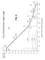
- FIG. 4 is a graph 400 that shows features of one example of the ramp signal 260 in accordance with the teachings of the present invention.
- a vertical axis of the graph 400 shows a relative amplitude of the ramp signal 260 with a maximum amplitude normalized to a value of one.
- a horizontal axis of the graph 400 shows the time after a beginning of a switching period as a percentage of a total switching period. Zero percent corresponds to a beginning of a period, and 100 percent corresponds to an end of a period.
- ramp signal 260 consists of pieces that are substantially straight lines. Therefore, the example ramp signal 260 in graph 400 is piecewise linear.
- Each straight line in the example ramp signal 260 in graph 400 is a segment.
- a segment that is neither horizontal (zero slope) nor vertical (infinite slope) has a finite linear slope in the graph 400.
- the segments of the ramp signal 260 that have finite linear slopes follow a horizontal segment 440 that has a slope of zero at a maximum amplitude of the ramp signal 260.
- the horizontal segment 440 constitutes a delay between a start of a switching period and a first segment that has a finite linear slope. Therefore, the ramp signal 260 is referred to as a delayed piecewise linear ramp.
- Each piece of the piecewise linear ramp signal 260 with a finite slope is a segment of the ramp.
- the example of FIG. 4 shows a delayed piecewise linear ramp with three segments that have finite linear slopes: SLOPE1 410, SLOPE2 420, and SLOPE3 430.
- the ramp signal 260 may have either more than three segments with finite linear slopes or fewer than three segments with finite linear slopes.
- the graph 400 shows that the example ramp signal 260 begins at its maximum value and maintains the maximum value until it begins to decrease in value at a point 405.
- the point 405 marks an end of a delay that in one example occurs when approximately 5.5 percent of a switching period has elapsed.
- the ramp signal 260 decreases in amplitude at a linear slope SLOPE1 410 until it reaches a point 415 that is approximately 0.272 times the maximum amplitude at approximately 53 percent of the switching period.
- the ramp signal 260 decreases in amplitude at a linear slope SLOPE2 420 until it reaches a point 425 that is approximately 0.139 times the maximum amplitude at approximately 75 percent of the switching period.
- the ramp signal 260 decreases in amplitude at a linear slope SLOPE3 430 until it reaches a point 435 that is approximately 0.059 times the maximum amplitude at approximately 99 percent of the switching period. It is appreciated that in other examples the values of magnitude and time at the points 405, 415, 425, and 435 may be different from the values in the example of FIG. 4 to achieve desired characteristics of an AC-DC power supply for a particular application.
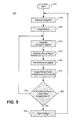
- FIG. 5 shows a flow diagram 500 that illustrates an example method in accordance with the teachings of the present invention.
- an integrator is initialized in a block 520.
- a power switch then closes in a block 530.
- an integrator integrates current in a power switch in a block 540.
- a ramp signal is generated in a block 550.
- an error signal is generated in a block 560 from a sensed output voltage and a reference.
- an amplitude of the ramp signal is scaled according the error signal.
- An amplitude of an integrated current signal is compared to an amplitude of a scaled ramp signal in a decision block 580. If the integrated current signal is less than the scaled ramp signal, the integration continues in block 540. If the integrated current signal is not less than the scaled ramp signal, the switch opens in block 590.
- the integrator is again initialized in block 520, and the flow repeats.
Abstract
Description
- The present invention relates generally to power supplies and, more specifically, the present invention relates to alternating current (AC) to direct current (DC) power supplies.
- A current having a frequency that is a multiple of the fundamental frequency of an AC power line is a harmonic current. Harmonic currents are a burden to the power generation and distribution system. Hence, regulatory agencies impose restrictions on the harmonic current that power supplies draw from the power line.
- It is well known that switching power supplies can be controlled so that the input current is directly proportional to the input voltage, making the power supply appear as a resistor to the power source. These techniques have been successful in reducing the harmonic current at the input of switching power supplies that use many different topologies, such as for example the boost, buck-boost, flyback, and single ended primary inductor converter ("SEPIC") topologies that are known in the art. In each of these topologies, the technique of making the power supply appear as a resistor to the power source is sufficient to allow an AC-to-DC power supply to meet the requirement of low harmonic current at the input.
- The same technique that makes a power supply appear as a resistor to a power source, however, does not meet the requirement for low harmonic current when it is applied to a buck switching converter topology. Whereas other converter topologies can take current from the input during an entire cycle of the AC input voltage, the buck converter takes current from the input only when the input voltage is greater than the output voltage. Therefore, the power supply appears as a resistor only during a portion of the cycle of the AC input voltage, and appears as an open circuit otherwise. As a result, the AC input has higher than acceptable harmonic current.
- The present invention will be described by way of exemplary embodiments, but not limitations, illustrated in the accompanying drawings in which like references denote similar elements, and in which:
-
FIG. 1 shows one example of an AC-to-DC power supply that uses one example of the present invention to reduce harmonic current drawn from an AC power source in accordance with the teachings of the present invention; -
FIG. 2 illustrates an example controller of the power supply ofFIG. 1 in greater detail in accordance with the teachings of the present invention; -
FIG. 3 illustrates another example of an AC-to-DC power supply that includes details of elements of a controller in accordance with the teachings of the present invention; -
FIG. 4 gives example salient features of a delayed piecewise linear ramp with values for one example in accordance with the teachings of the present invention; and -
FIG. 5 is a flow diagram that shows an example method in accordance with the teachings of the present invention. - Examples of a circuit and method for reducing the harmonic current at the input of an AC-to-DC power supply using a switching power converter with a novel controller are disclosed herein. In the following description, numerous specific details are set forth in order to provide a thorough understanding of the present invention.
It will be apparent, however, to one having ordinary skill in the art that the specific detail need not be employed to practice the present invention. In other instances, well-known materials or methods have not been described in detail in order to avoid obscuring the present invention. - Reference throughout this specification to "one embodiment," "an embodiment," "one example" or "an example" means that a particular feature, structure or characteristic described in connection with the embodiment is included in at least one embodiment or example of the present invention. Thus, the appearances of the phrases "in one embodiment," "in an embodiment," "in one example" or "in an example" in various places throughout this specification are not necessarily all referring to the same embodiment. Furthermore, the particular features, structures or characteristics may be combined in any suitable manner in one or more embodiments.
- Many AC-DC power supplies are required to have an AC input current with low harmonic content. Simple low-cost circuits that change an AC voltage to a DC voltage usually give unacceptable results because their AC input current contains large amplitudes at frequencies that are multiples of the fundamental frequency of the AC power line.
- As will be described, in one example of the present invention, a method and apparatus disclosed here for explanation purposes uses an integral of a switch current and a delayed piecewise linear ramp signal that has special characteristics to allow an AC-to-DC power supply using a buck converter topology to meet the requirements for low harmonic current at its input. In another example, the delayed piecewise linear ramp may also control a flyback converter, or any other suitable power converter topology, to meet requirements of reduced harmonic current at the input of an AC-to-DC power supply in accordance with the teachings of the present invention.
- Accordingly,
FIG. 1 is functional block diagram showing an example of an AC-to-DC power supply 100 that controls a switching converter to meet the requirements of low harmonic current at an AC input. Arectifier 110 receives anAC input 105 with a voltage VAC to produce a rectifiedDC voltage V RECT 120 on a smallfilter capacitor C1 115. In the example ofFIG. 1 , therectifier 110 is a full wave bridge rectifier. The rectifiedDC voltage V RECT 120 is measured with respect to acommon input return 180. In the example,capacitor C 1 115 is large enough to provide a reservoir for a high frequency switching current or switch current ID 150, but small enough to allow the rectifiedDC voltage V RECT 120 to go substantially to zero twice during every cycle of the voltage VAC at theAC input 105. - Those skilled in the art will recognize an example configuration of a
diode D1 125, aninductor L1 130, acapacitor C2 135, aswitch S1 160, and aload 145 inFIG. 1 to be a buck converter that has a low-side switch. A low-side switch has one end of the switch at an electrical potential that is the same electrical potential as theinput return 180. Theinput return 180 is the negative DC terminal of therectifier 110. In the example ofFIG. 1 , the buck converter with a low-side switch receives the rectifiedDC voltage V RECT 120 at its input. - In an alternate example, a buck converter with a high-side switch instead of a low-side switch may receive the rectified
DC voltage V RECT 120 at its input. A high-side switch has one end of the switch at an electrical potential that is the same electrical potential as a positive DC terminal of therectifier 110. - In other examples, well-known configurations of power converters that have transformer isolation can also benefit from teachings of embodiments of the invention. One example of a buck converter that has transformer isolation is the single-switch forward converter.
- Buck converter configurations that have transformer isolation and multiple switches can benefit from teachings of the invention by sensing current in multiple switches. Examples of buck converter configurations that use transformer isolation with multiple switches are the two-switch forward converter, the push-pull buck converter, the half bridge buck converter, and the full-bridge buck converter.
- According to various examples of the invention, different configurations of power converters receive the rectified DC voltage VRECT at their inputs. It is appreciated that the function of
diode D 1 125 may sometimes be realized with a switch, and thatS1 160, whether low-side or high-side, whether single or one of a plurality of switches, is a switch that conducts current either to or from the rectifiedDC voltage V RECT 120. - The buck converter with a low-side switch in the example of
FIG. 1 produces anoutput voltage Vo 140 on theoutput capacitor C2 135 and theload 145. In the example, acontroller 165 senses theoutput voltage V o 140 on theoutput capacitor C2 135 and theload 145 with a pair ofvoltage sense terminals 170. Thecontroller 165 also senses the switch current ID 150 in theswitch S1 160 as a sensedcurrent signal 155. - Any of the many known ways to sense current may be used to produce the sensed
current signal 155. For example, the switch current ID 150 may be sensed with a current transformer to produce the sensedcurrent signal 155 as a voltage or a current. In another example, theswitch current I D 150 may be sensed as a voltage across a discrete resistor. In yet another example, the switch current ID 150 may be sensed as a voltage between the drain and the source of a metal oxide semiconductor field effect transistor (MOSFET) that is used for theswitch S1 160. In one example,controller 165 andswitch S1 160 are on a same integrated circuit. - In the example of
FIG.1 , thecontroller 165 produces adrive signal 175 that controls or periodically opens and closesswitch S1 160 to substantially regulate theoutput voltage V o 140 while maintaining low harmonic current at theAC input 105. -
FIG. 2 is functional block diagram 200 that shows one example ofcontroller 165 of the example power supply ofFIG. 1 in greater detail in accordance with the teachings of the present invention. As shown, a sensedswitch current I DSENSE 205 may be received by aresetable integrator 210. In the example, theresetable integrator 210 is one that can be initialized upon receipt of a reset signal.Resetable integrator 210 integrates the sensed current IDSENSE 205 to produce a first input signal, which may also be referred to as an integratedcurrent signal 225, during a time when theswitch S1 160 is closed. In the example, an open switch does not conduct current. A closed switch may conduct current. In one example,resetable integrator 210 is reset to an initial state of zero when theswitch S1 160 is open. In the example ofFIG. 2 , the integratedcurrent signal 225 is a voltage VINT. - In the example of
FIG. 2 , adifferential amplifier 290 receives theoutput voltage Vo 140 at thevoltage sense terminals 170. Thedifferential amplifier 290 scales a magnitude of theoutput voltage Vo 140 to produce an outputsense voltage Vos 295 that is proportional to theoutput voltage V o 140 and is referenced to thecommon input return 180. - An error signal is a signal that represents a difference between an actual value and a desired value. Both the actual value and the desired value are proportional to a reference value. In the example of
FIG. 2 , anerror amplifier 280 is coupled to receive an output sense voltage fromdifferential amplifier 290 that is proportional to the output voltage of the power supply. Theerror amplifier 280 then produces anerror signal 275 that is an amplified difference between the outputsense voltage Vos 295 and areference voltage V REF 285. In the example ofFIG. 2 , theerror signal 275 is an error voltage VE. Thereference voltage V REF 285 is proportional to the desired value of theoutput voltage Vo 140. Theerror amplifier 280 inFIG. 2 includes a low pass filter that reduces an amplification of high frequency signals. In the example ofFIG. 2 , the reduction in amplification affects frequencies that are higher than a fraction of the frequency of the ACinput voltage V AC 105 ofFIG. 1 . Thus, the error signal 275 VE represents substantially an amplified difference between the actual value and the desired value of theoutput voltage Vo 140 averaged over a time period of several cycles of the ACinput voltage V AC 105 ofFIG. 1 . - In the example shown, an
oscillator circuit 240 provides signals and timing information for switching theswitch S1 160. Aclock signal 245 from theoscillator circuit 240 determines a switching period Ts of the switching cycles. The switching period Ts of a switching cycle is typically much smaller than a period of one cycle of the voltage at theAC input 105. In one example, the switching period Ts of a switching cycle is approximately 16 microseconds, whereas the period of a cycle of the voltage at theAC input 105 is approximately 16 milliseconds. Therefore, in one example, the switch switches approximately 1000 times during one cycle of the voltage at theAC input 105. - In the example of
FIG. 2 , theoscillator circuit 240 produces asignal 250 with the same switching period Ts as theclock signal 245. A ramp generator or aramp generator circuit 255 receives thesignal 250 to produce aramp signal 260 that is a voltage VRAMP with substantially the same switching period Ts as theclock signal 245, according to the example. The features of theramp signal 260 will be discussed later in this disclosure. In the example ofFIG. 2 , theramp generator circuit 255 constructs theramp signal 260 from portions of thesignal 250. In another example, a different ramp generator circuit may construct theramp signal 260 from only theclock signal 245. - In the example shown, a
multiplier circuit 265 receives theerror signal 275 as the error voltage VE and theramp signal 260 as a voltage VRAMP. Themultiplier circuit 265 produces a scaledramp signal 270 that is a product of the error signal 275 VE and the ramp signal 260 VRAMP divided by a normalizing voltage VNORM. Therefore, in the example ofFIG.2 , an output of themultiplier circuit 265 is a voltage kVRAMP that is proportional to theramp signal 260. The scaledramp signal 270 is thus responsive to both the ramp signal 260 VRAMP and the error signal 275 VE. - In the example shown, a
comparator 235 receives a first input signal, which is illustrated inFIG. 2 as integrated current signal 225 VINT, and a second input signal, which is illustrated inFIG. 2 as voltage kVRAMP of scaledramp signal 270. InFIG. 2 , an output ofcomparator 235 goes to a high logic level when the voltage of integrated current signal 225 VINT exceeds the voltage kVRAMP of the scaledramp signal 270. - In the example of
FIG. 2 , a drive signal generator, which may also be referred to asflip flop 220, is configured as a latch to receive theclock signal 245 at its clock input, abias voltage V BIAS 230 as a high logic level at its D input, and the output of thecomparator 235 at its reset input. The output Q of the flip-flop 220 is thedrive signal 175 of theswitch S1 160. In the example shown, theswitch S1 160 is closed when thedrive signal 175 is a high logic level. Theswitch S1 160 is open when thedrive signal 175 is a low logic level. - Thus, in the example shown, the
flip flop 220 is coupled to receive an input generated in response to both the integratedcurrent signal 225 and the scaledramp signal 220 to produce adrive signal 175 to be coupled to control aswitch S1 160 to substantially regulate anoutput voltage V o 140 of the power supply. - The
resetable integrator 210 receives acomplementary output 215 of the flip-flop 220 at its reset input. Therefore, theresetable integrator 210 is reset when theswitch S1 160 is open. - Next,
FIG. 3 shows another example of an AC-to-DC power supply 300 with another example of thecontroller 165 in accordance with the teachings of the present invention. In the AC-to-DC power supply 300 example ofFIG. 3 , theoutput voltage V o 140 is sensed without thedifferential amplifier 290 ofFIG. 2 . The AC-to-DC power supply ofFIG. 3 uses a sense winding 340 on a coupledinductor 305 to sense theoutput voltage Vo 140. According to the example shown, adiode D2 330 rectifies the voltage that appears on the sense winding 340 such that acapacitor C4 335 charges to an outputsense voltage Vos 295 referenced to thecommon input return 180, proportional to theoutput voltage V o 140. - In the example of
FIG. 3 , thecurrent sense signal 155 is received by aresetable integrator 325. Theresetable integrator 325 includes acurrent source 310 of a magnitude IDSENSE that is proportional to the switchcurrent I D 150. Thecurrent source 310 charges acapacitor C3 320 to produce the integratedcurrent signal 225 that is the voltage VINT.A switch S2 315 resets the integratedcurrent signal 225 to zero when thesignal 215 at the complementary output of the flip-flop 220 goes high. In the example ofFIG. 3 , switchesS1 160 andS2 315 are MOSFETs. -
FIG. 4 is agraph 400 that shows features of one example of theramp signal 260 in accordance with the teachings of the present invention. A vertical axis of thegraph 400 shows a relative amplitude of theramp signal 260 with a maximum amplitude normalized to a value of one. A horizontal axis of thegraph 400 shows the time after a beginning of a switching period as a percentage of a total switching period. Zero percent corresponds to a beginning of a period, and 100 percent corresponds to an end of a period. - As shown in the depicted example,
ramp signal 260 consists of pieces that are substantially straight lines. Therefore, theexample ramp signal 260 ingraph 400 is piecewise linear. Each straight line in theexample ramp signal 260 ingraph 400 is a segment. A segment that is neither horizontal (zero slope) nor vertical (infinite slope) has a finite linear slope in thegraph 400. The segments of theramp signal 260 that have finite linear slopes follow ahorizontal segment 440 that has a slope of zero at a maximum amplitude of theramp signal 260. Thehorizontal segment 440 constitutes a delay between a start of a switching period and a first segment that has a finite linear slope. Therefore, theramp signal 260 is referred to as a delayed piecewise linear ramp. - Each piece of the piecewise
linear ramp signal 260 with a finite slope is a segment of the ramp. The example ofFIG. 4 shows a delayed piecewise linear ramp with three segments that have finite linear slopes:SLOPE1 410,SLOPE2 420, andSLOPE3 430. In other examples, theramp signal 260 may have either more than three segments with finite linear slopes or fewer than three segments with finite linear slopes. - The
graph 400 shows that theexample ramp signal 260 begins at its maximum value and maintains the maximum value until it begins to decrease in value at apoint 405. Thepoint 405 marks an end of a delay that in one example occurs when approximately 5.5 percent of a switching period has elapsed. After the delay atpoint 405, theramp signal 260 decreases in amplitude at alinear slope SLOPE1 410 until it reaches apoint 415 that is approximately 0.272 times the maximum amplitude at approximately 53 percent of the switching period. From apoint 415, theramp signal 260 decreases in amplitude at alinear slope SLOPE2 420 until it reaches apoint 425 that is approximately 0.139 times the maximum amplitude at approximately 75 percent of the switching period. From thepoint 425, theramp signal 260 decreases in amplitude at alinear slope SLOPE3 430 until it reaches apoint 435 that is approximately 0.059 times the maximum amplitude at approximately 99 percent of the switching period. It is appreciated that in other examples the values of magnitude and time at thepoints FIG. 4 to achieve desired characteristics of an AC-DC power supply for a particular application. - Finally,
FIG. 5 shows a flow diagram 500 that illustrates an example method in accordance with the teachings of the present invention. After starting in ablock 510, an integrator is initialized in ablock 520. A power switch then closes in ablock 530. Next, in the example, an integrator integrates current in a power switch in ablock 540. A ramp signal is generated in ablock 550. Next, an error signal is generated in ablock 560 from a sensed output voltage and a reference. In ablock 570, an amplitude of the ramp signal is scaled according the error signal. An amplitude of an integrated current signal is compared to an amplitude of a scaled ramp signal in adecision block 580. If the integrated current signal is less than the scaled ramp signal, the integration continues inblock 540. If the integrated current signal is not less than the scaled ramp signal, the switch opens inblock 590. The integrator is again initialized inblock 520, and the flow repeats. - In the foregoing detailed description, the method and apparatus of the present invention has been described with reference to specific exemplary embodiments thereof. It will, however, be evident that various modifications and changes may be made thereto without departing from the broader spirit and scope of the present invention. The present specification and figures are accordingly to be regarded as illustrative rather than restrictive.
Claims (20)
- A controller for use in a buck converter, comprising:an integrator to be coupled to receive a current sense signal representative of a current in a switch of the buck converter, the integrator to integrate the current sense signal to produce a first input signal;a ramp generator coupled to receive an oscillating signal having a same switching period as the switch, the ramp generator to generate a piecewise linear ramp signal in response to the oscillating signal, the piecewise linear ramp signal having a delay segment of substantially zero slope followed by a plurality segments having finite linear slopes within the switching period of the switch;a multiplier to multiply the piecewise linear ramp signal to produce a second input signal; anda drive signal generator coupled to receive a third input signal generated in response to the first and the second input signals to produce a drive signal to be coupled to control the switch to substantially regulate an output voltage of the buck converter.
- The controller of claim 1 wherein the delay segment is substantially at a maximum amplitude of the piecewise linear ramp signal from approximately a beginning of the switching period until approximately 5.5 percent of the switching period has elapsed.
- The controller of claim 1 wherein the delay segment is followed by approximately three segments having finite linear slopes within the switching period.
- The controller of claim 1 wherein a first segment starts at approximately a maximum amplitude of the piecewise linear ramp signal and ends at approximately 0.272 times the substantially maximum amplitude of the piecewise linear ramp signal.
- The controller of claim 1 wherein a second segment starts at approximately an end of a first segment and ends at approximately 0.139 times the substantially maximum amplitude of the piecewise linear ramp signal.
- The controller of claim 1 wherein a third segment starts at approximately an end of a second segment and ends at approximately 0.059 times the maximum amplitude of the piecewise linear ramp signal.
- The controller of claim 1 wherein a first segment starts at an approximate end of the delay segment and ends when approximately 53 percent of the switching period has passed.
- The controller of claim 1 wherein a second segment starts at an approximate end of a first segment and ends when approximately 75 percent of the switching period has passed.
- The controller of claim 1 wherein a third segment starts at an approximate end of a second segment and ends when approximately 99 percent of the switching period has passed.
- The controller of claim 1 wherein the switch is included in a same integrated circuit as the controller.
- The controller of claim 1 wherein the switch is a low-side switch of the buck converter.
- The controller of claim 1 wherein the buck converter includes transformer isolation.
- The controller of claim 1 wherein the multiplier is coupled to generate a scaled ramp signal that is responsive to the piecewise linear ramp signal and an error signal representative of an error in the output voltage of the buck converter.
- The controller of claim 13 wherein the buck converter includes a sense winding on a coupled inductor to sense an output sense voltage used to produce the error signal.
- The controller of claim 1 further comprising an oscillator coupled to generate the oscillating signal coupled to be received by the ramp generator and a clock signal coupled to be received by the drive signal generator.
- A method of controlling a buck converter, comprising:integrating a signal representative of a current in a switch of the buck converter to produce an integrated current signal;generating a scaled ramp signal in response to a piecewise linear ramp signal and an error signal that is generated in response to an output voltage of the buck converter, wherein the piecewise linear ramp signal includes a delay segment having a substantially zero slope followed by a plurality of segments having finite linear slopes within a switching period of the switch; andcomparing the scaled ramp signal with the integrated current signal to produce a drive signal to control the switch to substantially regulate the output voltage of the buck converter.
- The method of claim 16 wherein the piecewise linear ramp signal includes a delay segment that is substantially at a maximum amplitude of the piecewise linear ramp signal from approximately a beginning of the switching period until approximately 5.5 percent of the switching period has elapsed.
- The method of claim 16 wherein the piecewise linear ramp signal includes a first segment that begins after approximately 5.5 percent of the switching period has elapsed.
- The method of claim 16 wherein the piecewise linear ramp signal includes a second segment that begins after approximately 53 percent of the switching period has elapsed.
- The method of claim 16 wherein the piecewise linear ramp includes a third segment that begins after approximately 75 percent of the switching period has elapsed.
Applications Claiming Priority (1)
| Application Number | Priority Date | Filing Date | Title |
|---|---|---|---|
| US12/049,098 US7990127B2 (en) | 2008-03-14 | 2008-03-14 | Method and apparatus for AC to DC power conversion with reduced harmonic current |
Publications (2)
| Publication Number | Publication Date |
|---|---|
| EP2101400A2 true EP2101400A2 (en) | 2009-09-16 |
| EP2101400A3 EP2101400A3 (en) | 2015-07-15 |
Family
ID=40732240
Family Applications (1)
| Application Number | Title | Priority Date | Filing Date |
|---|---|---|---|
| EP09154933.7A Withdrawn EP2101400A3 (en) | 2008-03-14 | 2009-03-11 | Method and apparatus for AC to DC power conversion with reduced harmonic current |
Country Status (4)
| Country | Link |
|---|---|
| US (1) | US7990127B2 (en) |
| EP (1) | EP2101400A3 (en) |
| JP (1) | JP2009225658A (en) |
| CN (1) | CN101546961B (en) |
Families Citing this family (15)
| Publication number | Priority date | Publication date | Assignee | Title |
|---|---|---|---|---|
| US8098506B2 (en) | 2009-06-02 | 2012-01-17 | Power Integrations, Inc. | Single-stage power supply with power factor correction and constant current output |
| US8558522B2 (en) * | 2010-12-18 | 2013-10-15 | Semiconductor Components Industries, Llc | Method for scaling a drive signal and circuit therefor |
| US9048744B2 (en) | 2011-01-03 | 2015-06-02 | Enphase Energy, Inc. | Method and apparatus for resonant converter control |
| FR2971102B1 (en) * | 2011-02-01 | 2019-09-06 | Safran Landing Systems | METHOD FOR LIMITING A CURRENT PROVIDED BY A DIRECT CURRENT POWER SOURCE. |
| US8963529B2 (en) * | 2011-04-28 | 2015-02-24 | Texas Instruments Incorporated | Transition mode charge control for a power converter |
| CN102324843B (en) * | 2011-05-17 | 2013-09-04 | 浙江大学 | High-precision sectional type linear slope compensation circuit |
| KR101365362B1 (en) | 2012-12-27 | 2014-02-24 | 삼성전기주식회사 | Average current controller, average current control method and buck converter using the average current controller |
| FR3008258B1 (en) * | 2013-07-04 | 2018-11-02 | Safran Electronics & Defense | AC / DC CONVERTER WITH GALVANIC ISOLATION AND SIGNAL CORRECTOR |
| CN104467376B (en) * | 2013-09-17 | 2017-04-12 | 力智电子股份有限公司 | Ramp signal generation method and generator, and PWM signal generator |
| TWI495974B (en) * | 2013-09-17 | 2015-08-11 | Upi Semiconductor Corp | Ramp signal generating method and generator thereof, and pulse width modulation signal generator |
| US9595876B2 (en) * | 2015-02-11 | 2017-03-14 | Schneider Electric It Corporation | DC-DC converter |
| US20180302017A1 (en) * | 2017-04-12 | 2018-10-18 | Power Integrations, Inc. | Current sense circuit for a dc motor inverter |
| US10418907B1 (en) | 2018-06-18 | 2019-09-17 | M3 Technology Inc. | Control circuit and method for switching power converters |
| CN111082675A (en) * | 2019-12-31 | 2020-04-28 | 上海晶丰明源半导体股份有限公司 | Low-power-consumption power conversion circuit for control panel |
| CN111162683B (en) | 2020-01-22 | 2021-09-14 | 上海晶丰明源半导体股份有限公司 | Power conversion circuit and method thereof |
Family Cites Families (24)
| Publication number | Priority date | Publication date | Assignee | Title |
|---|---|---|---|---|
| US4357572A (en) * | 1981-03-26 | 1982-11-02 | Bell Telephone Laboratories, Incorporated | Current flare out limit control for PWM converter |
| US4816982A (en) * | 1987-11-23 | 1989-03-28 | Viteq Corporation | AC to DC power converter with integrated line current control for improving power factor |
| US4975820A (en) * | 1989-09-01 | 1990-12-04 | National Semiconductor Corporation | Adaptive compensating ramp generator for current-mode DC/DC converters |
| US5479090A (en) * | 1993-11-24 | 1995-12-26 | Raytheon Company | Power converter having optimal dynamic operation |
| US6191676B1 (en) * | 1994-10-21 | 2001-02-20 | Spinel Llc | Apparatus for suppressing nonlinear current drawing characteristics |
| US5804950A (en) | 1996-06-20 | 1998-09-08 | Micro Linear Corporation | Input current modulation for power factor correction |
| KR100286047B1 (en) * | 1998-05-15 | 2001-04-16 | 김덕중 | Power factor correction(pfc) circuit using reverse sawtooth wave |
| US6448744B1 (en) * | 2000-10-30 | 2002-09-10 | International Business Machines Corporation | Power factor correction circuit |
| US6381154B1 (en) * | 2001-03-16 | 2002-04-30 | Tranh To Nguyen | PWM nonlinear controller with a single cycle response and a non resettable integrator |
| US6900995B2 (en) * | 2001-11-29 | 2005-05-31 | Iwatt, Inc. | PWM power converter controlled by transistion detection of a comparator error signal |
| US6853563B1 (en) | 2003-07-28 | 2005-02-08 | System General Corp. | Primary-side controlled flyback power converter |
| US7057440B2 (en) | 2003-11-03 | 2006-06-06 | System General Corp. | Multiplier-divider circuit for a PFC controller |
| US7054170B2 (en) | 2004-01-05 | 2006-05-30 | System General Corp. | Power-mode controlled power converter |
| US7061225B2 (en) | 2004-06-29 | 2006-06-13 | System General Corp. | Apparatus and method thereof for measuring output current from primary side of power converter |
| US6977824B1 (en) | 2004-08-09 | 2005-12-20 | System General Corp. | Control circuit for controlling output current at the primary side of a power converter |
| US7016204B2 (en) | 2004-08-12 | 2006-03-21 | System General Corp. | Close-loop PWM controller for primary-side controlled power converters |
| US7061780B2 (en) | 2004-09-09 | 2006-06-13 | System General Corp. | Switching control circuit with variable switching frequency for primary-side-controlled power converters |
| US7345464B2 (en) * | 2004-09-16 | 2008-03-18 | Semiconductor Components Industries, L.L.C. | PWM power supply controller having multiple PWM signal assertions and method therefor |
| US7259972B2 (en) | 2004-10-07 | 2007-08-21 | System General Corporation | Primary-side-control power converter having a switching controller using frequency hopping and voltage and current control loops |
| JP4678215B2 (en) * | 2005-03-15 | 2011-04-27 | サンケン電気株式会社 | Switching power supply |
| TWI307203B (en) * | 2005-06-03 | 2009-03-01 | Richtek Technology Corp | A pulse width modulation system with nonlinear ramp |
| US7352595B2 (en) | 2005-11-08 | 2008-04-01 | System General Corp. | Primary-side controlled switching regulator |
| US7639517B2 (en) | 2007-02-08 | 2009-12-29 | Linear Technology Corporation | Adaptive output current control for switching circuits |
| GB2447874B (en) * | 2007-03-30 | 2009-07-29 | Cambridge Semiconductor Ltd | Forward power converter controllers |
-
2008
- 2008-03-14 US US12/049,098 patent/US7990127B2/en not_active Expired - Fee Related
-
2009
- 2009-03-11 EP EP09154933.7A patent/EP2101400A3/en not_active Withdrawn
- 2009-03-13 JP JP2009060765A patent/JP2009225658A/en not_active Withdrawn
- 2009-03-16 CN CN200910127165.4A patent/CN101546961B/en not_active Expired - Fee Related
Also Published As
| Publication number | Publication date |
|---|---|
| US7990127B2 (en) | 2011-08-02 |
| CN101546961A (en) | 2009-09-30 |
| JP2009225658A (en) | 2009-10-01 |
| EP2101400A3 (en) | 2015-07-15 |
| US20090231889A1 (en) | 2009-09-17 |
| CN101546961B (en) | 2014-03-19 |
Similar Documents
| Publication | Publication Date | Title |
|---|---|---|
| US7990127B2 (en) | Method and apparatus for AC to DC power conversion with reduced harmonic current | |
| US9618955B2 (en) | Method and apparatus to increase efficiency in a power factor correction circuit | |
| US9859788B2 (en) | Power factor correction circuit and switching power supply apparatus | |
| US8593127B2 (en) | Method and apparatus to reduce line current harmonics from a power supply | |
| US8749212B2 (en) | Method and apparatus to control a power factor correction circuit | |
| US7518895B2 (en) | High-efficiency power converter system | |
| US8320139B2 (en) | Switching regulator with frequency limitation and method thereof | |
| US8456868B2 (en) | Controller for a resonant switched-mode power converter | |
| US6307361B1 (en) | Method and apparatus for regulating the input impedance of PWM converters | |
| US8189355B2 (en) | Multiple output switching power source apparatus | |
| JP2010284071A (en) | Control apparatus for power supply | |
| US11601044B2 (en) | Method for driving an electronic switch in a power converter circuit and control circuit | |
| US20110194316A1 (en) | Switching power supply device | |
| US8634210B2 (en) | DC-DC converter including switching frequency control circuit | |
| US11139730B2 (en) | Burst controller and burst control method of resonance converter | |
| JP6810150B2 (en) | Switching power supply and semiconductor device | |
| JP2003125585A (en) | Power unit |
Legal Events
| Date | Code | Title | Description |
|---|---|---|---|
| PUAI | Public reference made under article 153(3) epc to a published international application that has entered the european phase |
Free format text: ORIGINAL CODE: 0009012 |
|
| 17P | Request for examination filed |
Effective date: 20090311 |
|
| AK | Designated contracting states |
Kind code of ref document: A2 Designated state(s): AT BE BG CH CY CZ DE DK EE ES FI FR GB GR HR HU IE IS IT LI LT LU LV MC MK MT NL NO PL PT RO SE SI SK TR |
|
| AX | Request for extension of the european patent |
Extension state: AL BA RS |
|
| PUAL | Search report despatched |
Free format text: ORIGINAL CODE: 0009013 |
|
| AK | Designated contracting states |
Kind code of ref document: A3 Designated state(s): AT BE BG CH CY CZ DE DK EE ES FI FR GB GR HR HU IE IS IT LI LT LU LV MC MK MT NL NO PL PT RO SE SI SK TR |
|
| AX | Request for extension of the european patent |
Extension state: AL BA RS |
|
| RIC1 | Information provided on ipc code assigned before grant |
Ipc: H02M 1/42 20070101AFI20150610BHEP |
|
| 17Q | First examination report despatched |
Effective date: 20150717 |
|
| AKX | Designation fees paid |
Designated state(s): AT BE BG CH CY CZ DE DK EE ES FI FR GB GR HR HU IE IS IT LI LT LU LV MC MK MT NL NO PL PT RO SE SI SK TR |
|
| AXX | Extension fees paid |
Extension state: AL Extension state: BA Extension state: RS |
|
| STAA | Information on the status of an ep patent application or granted ep patent |
Free format text: STATUS: THE APPLICATION IS DEEMED TO BE WITHDRAWN |
|
| 18D | Application deemed to be withdrawn |
Effective date: 20151118 |