US6900995B2 - PWM power converter controlled by transistion detection of a comparator error signal - Google Patents
PWM power converter controlled by transistion detection of a comparator error signal Download PDFInfo
- Publication number
- US6900995B2 US6900995B2 US10/306,719 US30671902A US6900995B2 US 6900995 B2 US6900995 B2 US 6900995B2 US 30671902 A US30671902 A US 30671902A US 6900995 B2 US6900995 B2 US 6900995B2
- Authority
- US
- United States
- Prior art keywords
- switch
- output
- feedback signal
- output voltage
- converter
- Prior art date
- Legal status (The legal status is an assumption and is not a legal conclusion. Google has not performed a legal analysis and makes no representation as to the accuracy of the status listed.)
- Expired - Lifetime, expires
Links
- 238000001514 detection method Methods 0.000 title description 2
- 238000000034 method Methods 0.000 claims abstract description 49
- 230000004044 response Effects 0.000 claims abstract description 18
- 230000001105 regulatory effect Effects 0.000 claims abstract description 14
- 230000001351 cycling effect Effects 0.000 claims abstract description 10
- 238000004804 winding Methods 0.000 claims description 29
- 230000007704 transition Effects 0.000 claims description 25
- 230000004907 flux Effects 0.000 claims description 9
- 230000001276 controlling effect Effects 0.000 claims description 7
- 238000012544 monitoring process Methods 0.000 claims 1
- 230000002401 inhibitory effect Effects 0.000 abstract 1
- 230000033228 biological regulation Effects 0.000 description 27
- 238000005070 sampling Methods 0.000 description 11
- 230000010355 oscillation Effects 0.000 description 10
- 238000011217 control strategy Methods 0.000 description 4
- 239000003990 capacitor Substances 0.000 description 3
- 238000010586 diagram Methods 0.000 description 3
- 238000002955 isolation Methods 0.000 description 3
- 238000005457 optimization Methods 0.000 description 3
- 230000008901 benefit Effects 0.000 description 2
- 230000003247 decreasing effect Effects 0.000 description 2
- 230000008569 process Effects 0.000 description 2
- 230000004913 activation Effects 0.000 description 1
- 230000005540 biological transmission Effects 0.000 description 1
- 230000008859 change Effects 0.000 description 1
- 238000006243 chemical reaction Methods 0.000 description 1
- 230000007423 decrease Effects 0.000 description 1
- 230000008034 disappearance Effects 0.000 description 1
- 230000000694 effects Effects 0.000 description 1
- 230000005669 field effect Effects 0.000 description 1
- 238000001914 filtration Methods 0.000 description 1
- 238000005259 measurement Methods 0.000 description 1
- 230000004048 modification Effects 0.000 description 1
- 238000012986 modification Methods 0.000 description 1
- 230000003071 parasitic effect Effects 0.000 description 1
Images


Classifications
-
- H—ELECTRICITY
- H02—GENERATION; CONVERSION OR DISTRIBUTION OF ELECTRIC POWER
- H02M—APPARATUS FOR CONVERSION BETWEEN AC AND AC, BETWEEN AC AND DC, OR BETWEEN DC AND DC, AND FOR USE WITH MAINS OR SIMILAR POWER SUPPLY SYSTEMS; CONVERSION OF DC OR AC INPUT POWER INTO SURGE OUTPUT POWER; CONTROL OR REGULATION THEREOF
- H02M3/00—Conversion of dc power input into dc power output
- H02M3/02—Conversion of dc power input into dc power output without intermediate conversion into ac
- H02M3/04—Conversion of dc power input into dc power output without intermediate conversion into ac by static converters
- H02M3/10—Conversion of dc power input into dc power output without intermediate conversion into ac by static converters using discharge tubes with control electrode or semiconductor devices with control electrode
- H02M3/145—Conversion of dc power input into dc power output without intermediate conversion into ac by static converters using discharge tubes with control electrode or semiconductor devices with control electrode using devices of a triode or transistor type requiring continuous application of a control signal
- H02M3/155—Conversion of dc power input into dc power output without intermediate conversion into ac by static converters using discharge tubes with control electrode or semiconductor devices with control electrode using devices of a triode or transistor type requiring continuous application of a control signal using semiconductor devices only
- H02M3/156—Conversion of dc power input into dc power output without intermediate conversion into ac by static converters using discharge tubes with control electrode or semiconductor devices with control electrode using devices of a triode or transistor type requiring continuous application of a control signal using semiconductor devices only with automatic control of output voltage or current, e.g. switching regulators
- H02M3/157—Conversion of dc power input into dc power output without intermediate conversion into ac by static converters using discharge tubes with control electrode or semiconductor devices with control electrode using devices of a triode or transistor type requiring continuous application of a control signal using semiconductor devices only with automatic control of output voltage or current, e.g. switching regulators with digital control
-
- H—ELECTRICITY
- H02—GENERATION; CONVERSION OR DISTRIBUTION OF ELECTRIC POWER
- H02M—APPARATUS FOR CONVERSION BETWEEN AC AND AC, BETWEEN AC AND DC, OR BETWEEN DC AND DC, AND FOR USE WITH MAINS OR SIMILAR POWER SUPPLY SYSTEMS; CONVERSION OF DC OR AC INPUT POWER INTO SURGE OUTPUT POWER; CONTROL OR REGULATION THEREOF
- H02M3/00—Conversion of dc power input into dc power output
- H02M3/02—Conversion of dc power input into dc power output without intermediate conversion into ac
- H02M3/04—Conversion of dc power input into dc power output without intermediate conversion into ac by static converters
- H02M3/10—Conversion of dc power input into dc power output without intermediate conversion into ac by static converters using discharge tubes with control electrode or semiconductor devices with control electrode
- H02M3/145—Conversion of dc power input into dc power output without intermediate conversion into ac by static converters using discharge tubes with control electrode or semiconductor devices with control electrode using devices of a triode or transistor type requiring continuous application of a control signal
- H02M3/155—Conversion of dc power input into dc power output without intermediate conversion into ac by static converters using discharge tubes with control electrode or semiconductor devices with control electrode using devices of a triode or transistor type requiring continuous application of a control signal using semiconductor devices only
- H02M3/156—Conversion of dc power input into dc power output without intermediate conversion into ac by static converters using discharge tubes with control electrode or semiconductor devices with control electrode using devices of a triode or transistor type requiring continuous application of a control signal using semiconductor devices only with automatic control of output voltage or current, e.g. switching regulators
-
- H—ELECTRICITY
- H02—GENERATION; CONVERSION OR DISTRIBUTION OF ELECTRIC POWER
- H02M—APPARATUS FOR CONVERSION BETWEEN AC AND AC, BETWEEN AC AND DC, OR BETWEEN DC AND DC, AND FOR USE WITH MAINS OR SIMILAR POWER SUPPLY SYSTEMS; CONVERSION OF DC OR AC INPUT POWER INTO SURGE OUTPUT POWER; CONTROL OR REGULATION THEREOF
- H02M3/00—Conversion of dc power input into dc power output
- H02M3/22—Conversion of dc power input into dc power output with intermediate conversion into ac
- H02M3/24—Conversion of dc power input into dc power output with intermediate conversion into ac by static converters
- H02M3/28—Conversion of dc power input into dc power output with intermediate conversion into ac by static converters using discharge tubes with control electrode or semiconductor devices with control electrode to produce the intermediate ac
- H02M3/325—Conversion of dc power input into dc power output with intermediate conversion into ac by static converters using discharge tubes with control electrode or semiconductor devices with control electrode to produce the intermediate ac using devices of a triode or a transistor type requiring continuous application of a control signal
- H02M3/335—Conversion of dc power input into dc power output with intermediate conversion into ac by static converters using discharge tubes with control electrode or semiconductor devices with control electrode to produce the intermediate ac using devices of a triode or a transistor type requiring continuous application of a control signal using semiconductor devices only
- H02M3/33507—Conversion of dc power input into dc power output with intermediate conversion into ac by static converters using discharge tubes with control electrode or semiconductor devices with control electrode to produce the intermediate ac using devices of a triode or a transistor type requiring continuous application of a control signal using semiconductor devices only with automatic control of the output voltage or current, e.g. flyback converters
- H02M3/33515—Conversion of dc power input into dc power output with intermediate conversion into ac by static converters using discharge tubes with control electrode or semiconductor devices with control electrode to produce the intermediate ac using devices of a triode or a transistor type requiring continuous application of a control signal using semiconductor devices only with automatic control of the output voltage or current, e.g. flyback converters with digital control
-
- H—ELECTRICITY
- H02—GENERATION; CONVERSION OR DISTRIBUTION OF ELECTRIC POWER
- H02M—APPARATUS FOR CONVERSION BETWEEN AC AND AC, BETWEEN AC AND DC, OR BETWEEN DC AND DC, AND FOR USE WITH MAINS OR SIMILAR POWER SUPPLY SYSTEMS; CONVERSION OF DC OR AC INPUT POWER INTO SURGE OUTPUT POWER; CONTROL OR REGULATION THEREOF
- H02M3/00—Conversion of dc power input into dc power output
- H02M3/22—Conversion of dc power input into dc power output with intermediate conversion into ac
- H02M3/24—Conversion of dc power input into dc power output with intermediate conversion into ac by static converters
- H02M3/28—Conversion of dc power input into dc power output with intermediate conversion into ac by static converters using discharge tubes with control electrode or semiconductor devices with control electrode to produce the intermediate ac
- H02M3/325—Conversion of dc power input into dc power output with intermediate conversion into ac by static converters using discharge tubes with control electrode or semiconductor devices with control electrode to produce the intermediate ac using devices of a triode or a transistor type requiring continuous application of a control signal
- H02M3/335—Conversion of dc power input into dc power output with intermediate conversion into ac by static converters using discharge tubes with control electrode or semiconductor devices with control electrode to produce the intermediate ac using devices of a triode or a transistor type requiring continuous application of a control signal using semiconductor devices only
- H02M3/33507—Conversion of dc power input into dc power output with intermediate conversion into ac by static converters using discharge tubes with control electrode or semiconductor devices with control electrode to produce the intermediate ac using devices of a triode or a transistor type requiring continuous application of a control signal using semiconductor devices only with automatic control of the output voltage or current, e.g. flyback converters
- H02M3/33523—Conversion of dc power input into dc power output with intermediate conversion into ac by static converters using discharge tubes with control electrode or semiconductor devices with control electrode to produce the intermediate ac using devices of a triode or a transistor type requiring continuous application of a control signal using semiconductor devices only with automatic control of the output voltage or current, e.g. flyback converters with galvanic isolation between input and output of both the power stage and the feedback loop
-
- H—ELECTRICITY
- H02—GENERATION; CONVERSION OR DISTRIBUTION OF ELECTRIC POWER
- H02M—APPARATUS FOR CONVERSION BETWEEN AC AND AC, BETWEEN AC AND DC, OR BETWEEN DC AND DC, AND FOR USE WITH MAINS OR SIMILAR POWER SUPPLY SYSTEMS; CONVERSION OF DC OR AC INPUT POWER INTO SURGE OUTPUT POWER; CONTROL OR REGULATION THEREOF
- H02M1/00—Details of apparatus for conversion
- H02M1/0003—Details of control, feedback or regulation circuits
- H02M1/0041—Control circuits in which a clock signal is selectively enabled or disabled
Definitions
- the invention pertains generally to the field of power conversion and more particularly to methods of controlling power converters.
- Switching power converters offer both compactness and efficiency in a number of different topologies that can be placed in two main categories: isolated (or transformer-coupled) and non-isolated (or direct-coupled).
- non-isolated switching power converters such as a buck (reducing voltage) or boost (increasing voltage) converter
- the power output is directly coupled to the power input through the power switch element.
- isolated power converters such as flyback or forward converters
- the power output is isolated from the power input through a transformer, with the power switch element located on the primary (input) side of the transformer.
- the regulation of the output voltage of switching power converters is generally accomplished by sensing the difference between an output voltage feedback signal approximating the output voltage at the load, and a reference, and using this difference, or error voltage, to determine how to cycle the switch so as to minimize the difference between the output voltage feedback signal and the reference.
- regulation schemes can be divided into two classes: pulse modulating schemes and pulse gating schemes.
- the error voltage is used to form a pulse which will cycle the switch in such a way as to drive the output voltage signal onto the reference; whereas with pulse gating schemes, the error voltage is not used to form a specific pulse, but instead is used to gate pre-formed pulses (from a pulse generator) to the switch to drive the output voltage feedback signal toward the reference.
- Pulse width modulation PWM
- PFM pulse frequency modulation
- combinations of PWM and PFM form the basis of most pulse modulating schemes.
- the converter 10 includes a power switch Q 1 (typically a field effect transistor (FET)) coupled to an input voltage, V in , via a primary winding 20 of a power transformer T 1 .
- a rectifying diode D 1 and filter capacitor C 1 are coupled to a secondary winding 22 of the transformer T 1 .
- the converter 10 includes a pulse modulating controller 25 that outputs a drive signal 61 to turn ON the power switch Q 1 in order to control an output voltage, V out , across a load 24 .
- a primary/secondary isolation circuit 30 provides an output voltage feedback signal that approximates the output voltage across load 24 .
- An error voltage sense circuit 31 generates an error voltage from inputs that include a reference voltage, V REF , as well as the output voltage feedback signal from primary/secondary isolation circuit 30 . This error voltage is used by the controller 25 for regulating the ON time of the power switch Q 1 .
- FIG. 2 illustrates a flyback converter 15 , which is similar to converter 10 of FIG. 1 , except that the reflected output voltage feedback signal is obtained from a primary-side an auxiliary winding 40 , instead of from the primary/secondary isolation circuit 30 .
- the voltage, V AUX across the auxiliary winding 40 is proportional to the output voltage V out across the load 24 minus a voltage drop produced by resistive and other losses in the secondary circuit, including losses across the rectifying diode D 1 . These losses will vary, depending upon the current drawn by the load and other factors.
- a method for regulating voltage at an output of a switching power converter includes sensing an output voltage feedback signal; comparing the sensed feedback signal to a reference at a determined time during a cycling of the switch, and regulating the output voltage by controlling the turn-ON and turn-OFF times of a switch in response to an output of the comparison.
- the comparison may be accomplished by one of binary comparison logic, ternary comparison logic and signed digital comparison logic.
- the determined time is determined for each cycling of the switch.
- the methods may be used in conjunctions with both transformer-coupled and direct-coupled power converters.
- the power converter is a transformer-coupled power converter having its output coupled through a rectifying element, with the feedback signal originating from the primary side of the converter.
- the determined time is an instant at which the feedback signal corresponds to the output voltage at the load plus a small, substantially constant voltage drop measured from cycle to cycle of the switch.
- the determined time is an instant at which current flowing through a secondary rectifying element is small and substantially constant from cycle to cycle of the switch.
- the converter is a flyback converter
- the feedback signal is a reflected flyback voltage signal
- the determined time is a fixed backward offset time from the transformer flux reset point.
- the method includes determining the transformer flux reset point using a measured or calculated value of the period of resonant oscillation of the reflected flyback voltage signal.
- the method includes determining the transformer flux reset point based on a point at which voltage across an auxiliary transformer winding is approximately zero.
- the method includes determining the transformer flux reset point based on a point at which voltage across the primary winding of the power transformer is approximately zero.
- the converter is a forward converter
- the output voltage feedback signal is a reflected voltage across an auxiliary winding coupled to the output inductor
- the determined time is at a fixed backward offset time from a point of output inductor flux reset.
- the converter is a direct-coupled boost converter
- the output voltage feedback signal corresponds to a voltage across the switch during its off time
- the determined time is at an instant at which current through a rectifying element is small and substantially constant from cycle to cycle.
- the converter is a direct-coupled buck converter
- the output voltage feedback signal corresponds to a differential voltage across an output inductor during the off time of the high-side switch
- the determined time is at an instant at which current through a rectifying element is small and substantially constant from cycle to cycle.
- the pulse modulating controller takes into account comparisons from one or more previous switch cycles in determining the turn ON and turn OFF times of a switch in response to the present comparison output
- FIG. 1 is a flyback converter with a pulse modulating controller having prior art secondary-side feedback.
- FIG. 2 is a flyback converter with a pulse modulating controller having prior art primary-side feedback.
- FIG. 3 is a flyback converter with a pulse modulating controller having primary-only feedback according to one embodiment of the invention.
- FIGS. 4 and 5 are timing diagrams illustrating a primary-only feedback sampling technique according to embodiments of the invention.
- FIGS. 5A and 5B provide greater detail of aspects demonstrated in the timing diagrams in FIGS. 4 and 5 .
- FIG. 6 is a flyback converter with a pulse modulating controller having primary-only feedback according to another embodiment of the invention.
- FIG. 7 is a forward converter with a pulse modulating controller having primary-only feedback according to yet another embodiment of the invention.
- FIG. 8 is a non-isolated boost converter with a pulse modulating controller using primary-only feedback according to still another embodiment of the invention.
- FIG. 9 is a buck converter with a pulse modulating controller using primary-only feedback according to yet another embodiment of the invention.
- FIG. 10 is a logical flowchart of a signed digital comparator employed in embodiments of the invention.
- FIG. 11 is a logical flowchart of a signed digital early/late detector employed in embodiments of the invention.
- FIGS. 12A-B describe the operation of a pulse modulating controller implementing a high/low detector according to one embodiment of the invention.
- FIGS. 13A-B describe the operation of a pulse modulating controller implementing a ternary early/late detector according to another embodiment of the invention.
- FIGS. 14A-B describe the operation of a pulse modulating controller implementing a signed digital early/late detector according to yet another embodiment of the invention.
- transformer-coupled switching converters such as a flyback, forward, fly-forward, push-pull, or bridge-type power converters.
- direct-coupled switching power converters such as buck, boost, buck/boost or SEPIC power converters may also benefit from these control methodologies and embodiments.
- pulse rate regulation in itself, controls neither the ON TIME nor the OFF TIME of the power switch in order to regulate the output voltage.
- output regulation may be accomplished by controlling the rate of independently specified activation pulses presented to the power switch. If the load requires more power, pulses from a pulse generator are allowed to cycle the power switch. Otherwise, pulses from the pulse generator are inhibited from cycling the power switch.
- Control circuitry for and methods for obtaining accurate, real-time primary-only feedback are disclosed and described in the above-incorporated U.S. patents and applications, and are further refined upon herein. These primary-only circuits and methods may also be applied to power converters regulated using PWM and PFM controllers, as disclosed and described below.
- PWM and PFM controllers endeavor to construct pulses that will drive the output voltage onto the reference.
- the output voltage will “ripple” about the reference.
- pulse rate control parameters i.e., phase, width, and frequency
- pulse rate regulation presents the opportunity to realize numerous power stage optimizations obtained at the price of exchanging “ripples” for “limit cycles.”
- secondary feedback with its costly opto-isolator circuit and attendant demands on circuit board layout, primary-only feedback offers the potential of cheaper, slimmer power supplies for applications such as consumer electronics.
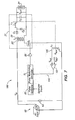
- FIG. 3 illustrates a flyback power converter 100 employing primary-only feedback for regulation purposes.
- the converter 100 includes a power stage 35 , which comprises a transformer T 1 having a primary winding 20 and secondary winding 22 , rectifying diode D 1 and filter capacitor C 1 .
- Power stage 35 receives an input voltage, V in , produced by a rectifier 92 operating on an AC line input.
- a capacitor 93 helps smooth voltage ripple on V in .
- a pulse modulating controller 70 produces a power pulse drive signal 71 that cycles switch Q 1 based on an output voltage feedback signal 150 .
- switch Q 1 may be a power MOSFET. Alternatively, switch Q 1 may comprise multiple transistors or other suitable means.
- pulse modulating controller 70 controls the ON TIME (the time between switch ON and switch OFF) and the OFF TIME (the time between switch OFF and switch ON) through drive signal 71 that cycles switch Q 1 .
- Driver 96 amplifies drive signal 71 to effect the turn ON and turn OFF of switch Q 1 .
- controller 70 implements fixed frequency pulse width modulation (PWM)
- PWM pulse width modulation
- the switch ON TIME will vary between a minimum power pulse width (corresponding to the minimum duty cycle) and a maximum power pulse width (corresponding to the maximum duty cycle).
- the switch OFF TIME will be the difference between the switch cycle period and the ON TIME.
- controller 70 implements fixed ON TIME pulse frequency modulation (PFM)
- the switch OFF TIME will vary between a minimum value (corresponding to the maximum duty cycle) and a maximum value (corresponding to the minimum duty cycle).
- controller 70 implements some combination of PWM and PFM
- the switch ON TIME and OFF TIME may be determined, in part, by operating conditions, such as the power being transferred to load 24 .
- the pulse modulating controller 70 may or may not keep history; that is it may or may not remember the results of previous comparisons. If controller 70 keeps history, it may reference said history in the process of determining the ON TIME and OFF TIME of switch Q 1 . Moreover, the precise instants in time when transistor Q 1 switches ON and OFF may further be controlled by a pulse optimizer 85 , as disclosed and described in the above-incorporated patents and applications, and described further herein.
- the flyback power converter 100 implements a method of primary-only feedback in the following fashion.
- switch Q 1 When switch Q 1 is switched OFF following the ON time of a power pulse, the voltage on the secondary winding 22 will be “reflected” back onto the primary winding 20 scaled by the turns ratio, N P /N S , where N P is the number of turns on the primary winding 20 and N S is the number or turns on the secondary winding 22 .
- V AUX ( V out + ⁇ V ) N AUX /N S (1) where ⁇ V is the voltage drop caused by resistive and other losses in the secondary circuit. This voltage drop includes, in particular, losses across rectifying diode D 1 .
- One aspect of the present invention leverages the notion that by sampling V AUX at precisely determined instants for which the term ⁇ V is small and approximately constant from sample to sample, real-time output voltage feedback can be obtained, where “real-time” output voltage feedback denotes an unfiltered output voltage measurement taken after each power pulse and available to the control logic for the selection of the succeeding drive signal.
- a comparator 151 produces an output voltage feedback signal 150 by comparing the V AUX waveform to a reference voltage, V REF , calibrated to compensate for the average value of ⁇ V at those precisely determined instants when ⁇ V is small and substantially constant from cycle to cycle.
- V REF a reference voltage
- the reference may be derived from a bandgap voltage reference or other suitable means, such as a compensated zener diode to provide a reliably stable reference voltage.
- Comparator 151 employed to generate feedback signal 150 can be more or less sophisticated, depending on the amount of information required to insure acceptable regulation. Perhaps the simplest of comparators is the binary comparator, with or without hysteresis, which indicates V AUX is high or low, relative to V REF . Slightly more sophisticated is the ternary comparator, which indicates high or low or neither, when the magnitude of the difference between V AUX and V REF is less than some fixed voltage.
- a still more sophisticated comparator is a signed digital comparator, which provides a high or low indication and, in addition, the magnitude of the difference expressed digitally.
- FIG. 10 details one embodiment of a signed digital comparator implemented with binary comparators, counters, a digital-to-analog converter, a subtractor, and a minimal amount of control logic, obviating the need for an error amplifier and the sample and hold circuitry characteristic of prior art analog systems.
- the comparator may indicate “high” by zero units of voltage.
- binary comparators without hysteresis are assumed.
- the sampling timing diagrams of FIG. 4 and FIG. 5 illustrate timing for both a “maximum” power pulse 106 and a “minimum” power pulse 107 generated by the pulse modulating controller 70 in converter 100 . Shown are the following waveforms: a) the drive signal 71 to transistor switch Q 1 , b) the auxiliary voltage waveform 102 , and c) the secondary current I SEC waveform 103 through the rectifying diode D 1 .
- the reflected auxiliary voltage waveform 102 swings high when drive signal 101 switches transistor Q 1 from ON to OFF.
- I SEC 103 will also jump from a substantially zero current to a relatively high current value, I PEAK , when drive signal 101 switches transistor Q 1 from ON to OFF.
- the ⁇ V term in equation (1) is maintained at a small and approximately constant value regardless of line or load conditions, enabling the potential for precise output regulation.
- An alternative to direct sensing of the secondary current is the sensing of the transformer reset condition directly or indirectly.
- I SEC 103 When I SEC 103 reaches zero the transformer T 1 may be denoted to be in a reset condition. This reset condition occurs when the energy in the primary winding 20 has been completely transferred to the secondary winding 22 . At such a point in time, the voltage across primary winding 20 will proceed to drop rapidly to zero.
- V AUX across the auxiliary winding 105 will also drop rapidly to (and through) zero volts, oscillating around zero until switch ON occurs.
- a zero crossing comparator (not illustrated) could monitor V AUX and detect when it first equals zero following switch OFF.
- another comparator (not illustrated) could detect when V IN first equals the drain voltage on transistor Q 1 , V DRN , which occurs when V AUX first equals zero. Because the time at which V AUX first equals zero (T AUXO ) lags transformer reset by a fixed amount of time, and it is more easily detected, it provides attractive means for indirectly measuring transformer reset time.
- reflected auxiliary voltage waveform 102 will have a plateau period during the OFF TIME following a power pulse. A condition in which reflected auxiliary voltage 102 equals zero will occur following this plateau period at time 110 .
- time difference between the first zero crossing point of V AUX 110 following the turn OFF of switch Q 1 , and the second zero crossing point of V AUX 111 it is possible to empirically derive the period of resonant oscillation following flux reset. This empirically derived value of the resonant oscillation period is useful in fixing the setback from T AUXO to the transformer reset point (see below).
- the reflected auxiliary voltage 102 achieves its first minimum at a time T 3 , which occurs midway between times 110 and 111 .
- This first minimum voltage point, or a subsequent minimum, may be advantageously used as the point when the ON period for the next pulse begins. Because the voltage at the drain of transistor Q 1 is also a minimum at time T 3 , the switching stresses and losses are minimized.
- the drain voltage is non-zero at time T 3 , it may be denoted as the zero-voltage switching time because this is as close to zero as the drain voltage will get.
- the pulse optimizer 85 accepts a variety of optimizer inputs, including V AUX , and applies these inputs to derive the timing, etc., of power pulses, in order to realize optimizations such as zero-voltage switching.
- an effective and easily-mechanized method for implementing zero-voltage switching is first, to detect the first and second zero-crossings of V AUX following the turn off of switch Q 1 ; second, to derive the period of resonant oscillation; and third, to adjust power pulses to turn on at the first zero-crossing of V AUX (T AUXO ), plus 1 ⁇ 4 of the resonant oscillation period, or T AUXO plus 1 ⁇ 4 of the resonant oscillation period plus an integral multiple of resonant oscillation periods.
- T SAMPLE could, for example, be determined from T AUXO by first subtracting 1 ⁇ 4 of the resonant oscillation period (to “locate” the transformer reset point), and then subtracting ⁇ T. Having determined the sampling time, T SAMPLE , controller 70 need only evaluate the binary output signal 150 of comparator 151 to determine whether at that instant V AUX is higher or lower than the expected value, V REF .
- control strategies may be employed to modulate pulse width or frequency based on binary output signal 150 at time T SAMPLE . These control strategies have as their primary objective, the determination of the duty cycle required to regulate the output voltage. Accordingly, they may be viewed as search strategies, exemplified by linear search, binary search, Newton-Raphson search, etc.
- FIGS. 12A-B illustrate a linear search strategy; the ON TIME of the nth pulse is denoted by T ON (n).
- pulse modulating controller 70 narrows the next power pulse (relative to the previous power pulse) so as to reduce the power transferred to the load 24 to maintain regulation.
- the narrowing procedure amounts to decreasing the pulse width (relative to the width of the previous pulse) by a fixed increment, T DELTA , subject to the minimum pulse width constraint.
- pulse modulating controller 70 widens the next power pulse (relative to the previous power pulse) so as to increase the power transferred to load 24 to maintain regulation.
- the widening procedure in this case, amounts to increasing the pulse width (relative to the width of the previous pulse) by a fixed increment, T DELTA , subject to the maximum pulse width constraint.
- T DELTA a fixed increment
- the search converges on the value of T ON required for regulation, and the output voltage V OUT across load 24 will be determined through the value of V REF .
- An alternative to sampling the binary output signal 150 at time T SAMPLE is to sample signal 150 periodically to detect the high to low transitions or state changes of said signal, and classify them as “early” or “late” relative to T SAMPLE , where an “early” transition is one that occurs before T SAMPLE , and a “late” transition is one that occurs after T SAMPLE .
- T SAMPLE is, by definition, the expected crossover point of V AUX with V REF , and therefore the expected transition point of binary output signal 150 .
- a high to low transition of output signal 150 corresponds to V AUX crossing V REF from above.
- FIGS. 5A-B a high to low transition of output signal 150 corresponds to V AUX crossing V REF from above.
- 5A-B illustrate the “equivalence” between the condition in which V AUX crosses V REF “early” (relative to T SAMPLE ) and the condition in which binary output signal 150 is “low” at T SAMPLE .
- the condition in which V AUX crosses V REF “late” (or not at all) corresponds to the condition in which binary output signal 150 is “high” at T SAMPLE .
- An early/late detector can be more or less sophisticated, depending on the amount of information required to insure acceptable regulation. Perhaps the simplest of early/late detectors is the binary detector, which indicates early or late, relative to T SAMPLE . Slightly more sophisticated is the ternary detector, which indicates early or late or neither, when the magnitude of the earliness or lateness is less than some fixed interval of time. A still more sophisticated early/late detector is a signed digital detector, which provides an early or late indication and, in addition, the magnitude of the earliness or lateness expressed digitally. FIG.
- FIG. 11 details one embodiment of a signed digital early/late detector implemented with binary comparators, counters, a subtractor, and a minimal amount of control logic, obviating the need for an error amplifier and the sample and hold circuitry characteristic of prior art analog systems.
- a transition of binary output signal 150 that occurs at precisely T SAMPLE will be classified (by the detector) as “early” by zero units of time.
- control strategies may be employed to modulate pulse width or frequency based on early/late detection of transitions of binary output signal 150 (relative to T SAMPLE ). These control strategies have as their primary objective, the determination of the duty cycle required to regulate the output voltage. Accordingly, they may be viewed as search strategies, exemplified by linear search, binary search, Newton-Raphson search, etc.
- FIGS. 13A-B illustrate a fixed step linear search strategy, implemented with a ternary early/late detector.
- the ON TIME of the nth pulse is denoted by T ON (n).
- pulse modulating controller 70 widens the next power pulse (relative to the previous power pulse) so as to increase the power transferred to the load 24 to maintain regulation.
- the widening procedure amounts to increasing the pulse width (relative to the width of the previous pulse) by a fixed increment, T DELTA , subject to the maximum pulse width constraint.
- pulse modulating controller 70 narrows the next power pulse (relative to the previous power pulse) so as to reduce the power transferred to load 24 to maintain regulation.
- the narrowing procedure in this case, amounts to decreasing the pulse width (relative to the width of the previous pulse) by a fixed increment, T DELTA , subject to the minimum pulse width constraint.
- pulse modulating controller 70 leaves the width of the next power pulse unchanged (relative to the previous power pulse). In this fashion, the search converges on the value of T ON required for regulation, and the output voltage V out across load 24 will be determined through the value of V REF .
- FIGS. 14A-B illustrate a proportional step search strategy implemented with a signed digital early/late detector.
- pulse modulating controller 70 increases or decreases the power pulse width (relative to the previous power pulse) by an amount proportional (through the scale factor, k) to the earliness or lateness, denoted by T E/L .
- T E/L the scale factor
- Minimum power pulses play an important role in the output voltage regulation scheme. Since output voltage feedback is based on the reflected voltage across the transformer T 1 , a power pulse (of some size) must be sent in order for a sample of the output voltage to be obtained. The more frequently the output is sampled, the better the regulation and the better the response to step changes in load. Accordingly, the minimum pulse and minimum duty cycle constraints of PWM and PFM controls support the objectives of tight regulation and rapid step response.
- controller 70 When load 24 becomes very light or is removed from flyback converter 100 of FIG. 3 , the pulse modulating controller 70 would be expected to command a continuous train of minimum power pulses 107 for transmission through power stage 35 . Although the energy content of minimum pulses 107 is small, in the absence of load 24 it is possible that the output voltage V out will rise to a level above the desired regulation set point. To maintain good regulation under low-load or no-load conditions, controller 70 may incorporate a “skip mode” of operation, wherein controller 70 inhibits pulsing for short periods.
- Controller 70 may detect that a low-load or no-load condition is true by measuring the frequency of minimum power pulses 107 transferred through power stage 35 . Alternatively, it may utilize the magnitude information provided by a signed digital comparator or signed digital early/late detector to detect the disappearance (or reappearance) of the load. Once in skip mode, the digital logic in controller 70 intersperses minimum pulses with no pulses, to maintain good regulation with an appropriate level of response to step changes in load without creating excessive audible noise. The process of interspersing minimum pulses could be pseudo-random (e.g., employing a linear feedback shift register).
- the pulse optimizer 85 and pulse modulating controller 70 may be implemented as software on a programmable processor, or may be formed by a single component.
- the flyback converter 300 illustrated in FIG. 6 has the functions of pulse optimization and pulse modulating controller formed by a state machine 170 fed by one or more binary comparators.
- the state machine 170 may contain a pulse generator (not illustrated) for generating a power pulse drive signal. Pulse timing may be supplied by pulse optimizer logic, and ON TIME and OFF TIME by pulse modulating controller logic. Moreover, should a skip mode be desired, state machine 170 could simply command its pulse generator to not generate a power pulse drive signal.
- flyback converter 100 Although the above discussion has been with respect to a flyback converter 100 , it will be appreciated that primary-only feedback methods of the present invention may be implemented in other isolated power converters such as a forward converter.
- FIG. 7 illustrates a forward converter 180 with a pulse modulating controller 70 using primary-only feedback to control a forward power stage 37 .
- Pulse optimizer 85 , comparator 151 , pulse modulating controller 70 , and driver 96 serve the same functions described previously with respect to the flyback converters of FIGS. 3 and 6 .
- the output voltage of forward converter 180 is not reflected across the power transformer T 1 (as in flyback converters). Instead, the reflected voltage of the output may be sensed via an auxiliary winding 105 coupled to the output inductor L 1 .
- the reflected voltage across the auxiliary winding 105 V AUX
- the pulse optimizer 85 and pulse modulating controller 70 may be implemented as software on a programmable processor, or may be formed by a single component.
- FIG. 8 illustrates a non-isolated boost converter 280 with a pulse modulating controller 70 using primary-only feedback to control a forward power stage 55 . While the logic of the pulse optimizer 85 and the pulse modulating controller 70 in converter 280 may be different from that employed in transformer-coupled flyback and forward converters, a primary-only feedback circuits and methods of the present invention may be nevertheless be implemented as shown.
- the voltage across the switch Q 1 during its OFF time provides a suitable approximation to the output voltage when sampled at those precisely determined instants for which the current through the rectifier diode D 1 is small and approximately constant, sample to sample (i.e., from switch cycle to switch cycle). While shown separately in FIG. 8 , it will be appreciated that the pulse optimizer 85 and pulse modulating controller 70 may be implemented as software on a programmable processor, or may be formed by a single component.
- FIG. 9 illustrates a buck converter 250 with a pulse modulating controller 70 using primary-only feedback to control a forward power stage 57 .
- the logic of the pulse optimizer 85 and the pulse modulating controller 70 in converter 250 may be different from that employed in transformer-coupled forward and flyback converters, a primary-only feedback method of the present invention may nevertheless be implemented as shown.
- the differential voltage across the output inductor during the OFF time of the switch Q 1 provides a suitable approximation to the output voltage when sampled at those precisely determined instants for which the current through the rectifier diode D 1 is small and approximately constant, sample to sample (i.e., switch cycle to switch cycle).
- the pulse optimizer 85 and pulse modulating controller 70 may be implemented as software on a programmable processor, or may be formed by a single component.
Landscapes
- Engineering & Computer Science (AREA)
- Power Engineering (AREA)
- Dc-Dc Converters (AREA)
- Inverter Devices (AREA)
Abstract
Description
V AUX=(V out +ΔV)N AUX /N S (1)
where ΔV is the voltage drop caused by resistive and other losses in the secondary circuit. This voltage drop includes, in particular, losses across rectifying diode D1.
Claims (17)
Priority Applications (4)
| Application Number | Priority Date | Filing Date | Title |
|---|---|---|---|
| US10/306,719 US6900995B2 (en) | 2001-11-29 | 2002-11-27 | PWM power converter controlled by transistion detection of a comparator error signal |
| PCT/US2003/035265 WO2004051834A1 (en) | 2002-11-27 | 2003-11-05 | Digital regulation of power converters using primary-only feedback |
| AU2003286908A AU2003286908A1 (en) | 2002-11-27 | 2003-11-05 | Digital regulation of power converters using primary-only feedback |
| US11/099,281 US20050169017A1 (en) | 2001-11-29 | 2005-04-04 | Methods for digital regulation of power converters using primary-only feedback |
Applications Claiming Priority (2)
| Application Number | Priority Date | Filing Date | Title |
|---|---|---|---|
| US33572301P | 2001-11-29 | 2001-11-29 | |
| US10/306,719 US6900995B2 (en) | 2001-11-29 | 2002-11-27 | PWM power converter controlled by transistion detection of a comparator error signal |
Related Child Applications (1)
| Application Number | Title | Priority Date | Filing Date |
|---|---|---|---|
| US11/099,281 Continuation US20050169017A1 (en) | 2001-11-29 | 2005-04-04 | Methods for digital regulation of power converters using primary-only feedback |
Publications (2)
| Publication Number | Publication Date |
|---|---|
| US20040052095A1 US20040052095A1 (en) | 2004-03-18 |
| US6900995B2 true US6900995B2 (en) | 2005-05-31 |
Family
ID=23312994
Family Applications (3)
| Application Number | Title | Priority Date | Filing Date |
|---|---|---|---|
| US10/306,719 Expired - Lifetime US6900995B2 (en) | 2001-11-29 | 2002-11-27 | PWM power converter controlled by transistion detection of a comparator error signal |
| US10/306,728 Expired - Fee Related US6862198B2 (en) | 2001-11-29 | 2002-11-27 | PWM power converter with digital sampling control circuitry |
| US11/099,281 Abandoned US20050169017A1 (en) | 2001-11-29 | 2005-04-04 | Methods for digital regulation of power converters using primary-only feedback |
Family Applications After (2)
| Application Number | Title | Priority Date | Filing Date |
|---|---|---|---|
| US10/306,728 Expired - Fee Related US6862198B2 (en) | 2001-11-29 | 2002-11-27 | PWM power converter with digital sampling control circuitry |
| US11/099,281 Abandoned US20050169017A1 (en) | 2001-11-29 | 2005-04-04 | Methods for digital regulation of power converters using primary-only feedback |
Country Status (3)
| Country | Link |
|---|---|
| US (3) | US6900995B2 (en) |
| AU (1) | AU2002354249A1 (en) |
| WO (1) | WO2003047079A2 (en) |
Cited By (34)
| Publication number | Priority date | Publication date | Assignee | Title |
|---|---|---|---|---|
| US20050195022A1 (en) * | 2004-03-05 | 2005-09-08 | Wen-Kei Lee | Booster |
| US6972969B1 (en) * | 2004-08-19 | 2005-12-06 | Iwatt, Inc. | System and method for controlling current limit with primary side sensing |
| US20060174939A1 (en) * | 2004-12-29 | 2006-08-10 | Isg Technologies Llc | Efficiency booster circuit and technique for maximizing power point tracking |
| US7248487B1 (en) | 2006-06-01 | 2007-07-24 | Cambridge Semiconductor Limited | Switch mode power supply controllers |
| US20070217232A1 (en) * | 2005-08-26 | 2007-09-20 | Djenguerian Alex B | Method and apparatus for digital control of a switching regulator |
| US20070236194A1 (en) * | 2006-04-10 | 2007-10-11 | Vo Hai H | Adaptive DC to DC converter system |
| US20070274106A1 (en) * | 2006-05-23 | 2007-11-29 | David Robert Coulson | Switch mode power supply controllers |
| US20070274107A1 (en) * | 2006-05-23 | 2007-11-29 | Garner David M | Switch mode power supply controllers |
| US20080007977A1 (en) * | 2006-07-07 | 2008-01-10 | Johan Piper | Switch mode power supply systems |
| US20080007982A1 (en) * | 2006-07-07 | 2008-01-10 | Johan Piper | Switch mode power supply systems |
| US20080037294A1 (en) * | 2006-05-23 | 2008-02-14 | Cambridge Semiconductor Limited | Switch mode power supply controllers |
| US20080063404A1 (en) * | 2004-09-20 | 2008-03-13 | Zxtalk Assets L.L.C. | Transmitting Device for Free-Space Optical Transmission |
| US20080089100A1 (en) * | 2006-10-13 | 2008-04-17 | Park Young-Bae | Switching mode power supply and driving method |
| US20080247202A1 (en) * | 2007-04-06 | 2008-10-09 | Power Integrations, Inc. | Method and apparatus for sensing multiple voltage values from a single terminal of a power converter controller |
| US20080246447A1 (en) * | 2007-04-06 | 2008-10-09 | Power Integrations, Inc. | Method and apparatus for integrated cable drop compensation of a power converter |
| US20080247199A1 (en) * | 2007-04-06 | 2008-10-09 | Power Integrations, Inc. | Method and apparatus for power converter fault condition detection |
| US20080246446A1 (en) * | 2007-04-06 | 2008-10-09 | Power Integrations, Inc. | Method and apparatus for on/off control of a power converter |
| US20090091309A1 (en) * | 1998-02-27 | 2009-04-09 | Power Integrations, Inc. | Off-line converter with digital control |
| US7551460B2 (en) | 2006-05-23 | 2009-06-23 | Cambridge Semiconductor Limited | Switch mode power supply controllers |
| US20090195229A1 (en) * | 2000-08-08 | 2009-08-06 | Power Integrations, Inc. | Method and apparatus for reducing audio noise in a switching regulator |
| US20090231889A1 (en) * | 2008-03-14 | 2009-09-17 | Power Integrations, Inc. | Method and apparatus for ac to dc power conversion with reduced harmonic current |
| US20090290390A1 (en) * | 2008-05-23 | 2009-11-26 | Johan Piper | Switched mode power supply systems |
| US20090296437A1 (en) * | 2008-05-29 | 2009-12-03 | Fairchild Korea Semiconductor Ltd., | Converter |
| US7738271B1 (en) | 2007-06-08 | 2010-06-15 | Science Applications International Corporation | Controlled resonant charge transfer device |
| US20100246216A1 (en) * | 2006-05-23 | 2010-09-30 | Cambridge Semiconductor Limited | Switch mode power supply controllers |
| US20100296318A1 (en) * | 2009-05-22 | 2010-11-25 | Yong Siang Teo | System and Method for Ringing Suppression in a Switched Mode Power Supply |
| US20100302811A1 (en) * | 2009-06-02 | 2010-12-02 | Power Integrations, Inc. | Single-stage power supply with power factor correction and constant current output |
| US20110090718A1 (en) * | 2009-10-21 | 2011-04-21 | Panasonic Corporation | Switching power supply device |
| US20110157922A1 (en) * | 2009-12-30 | 2011-06-30 | Pavel Konecny | Primary side sensing for isolated fly-back converters |
| US20110193494A1 (en) * | 2010-02-09 | 2011-08-11 | Power Integrations, Inc. | Integrated on-time extension for non-dissipative bleeding in a power supply |
| US20110194312A1 (en) * | 2010-02-09 | 2011-08-11 | Power Integrations, Inc. | Method and apparatus for determining zero-crossing of an ac input voltage to a power supply |
| US8030912B2 (en) | 2007-04-06 | 2011-10-04 | Power Integrations, Inc. | Method and apparatus for controlling the maximum output power of a power converter |
| US9263950B2 (en) | 2010-04-30 | 2016-02-16 | The Board Of Trustees Of The University Of Alabama | Coupled inductors for improved power converter |
| US9330826B1 (en) | 2010-02-12 | 2016-05-03 | The Board Of Trustees Of The University Of Alabama For And On Behalf Of The University Of Alabama | Integrated architecture for power converters |
Families Citing this family (60)
| Publication number | Priority date | Publication date | Assignee | Title |
|---|---|---|---|---|
| US7269034B2 (en) | 1997-01-24 | 2007-09-11 | Synqor, Inc. | High efficiency power converter |
| US7887551B2 (en) | 1999-12-02 | 2011-02-15 | Smith & Nephew, Inc. | Soft tissue attachment and repair |
| US7153312B1 (en) | 1999-12-02 | 2006-12-26 | Smith & Nephew Inc. | Closure device and method for tissue repair |
| US7697591B2 (en) * | 2002-08-26 | 2010-04-13 | Texas Instruments Incorporated | Crest factor reduction processor for wireless communications |
| US9314235B2 (en) * | 2003-02-05 | 2016-04-19 | Smith & Nephew, Inc. | Tissue anchor and insertion tool |
| US6927663B2 (en) * | 2003-07-23 | 2005-08-09 | Cardiac Pacemakers, Inc. | Flyback transformer wire attach method to printed circuit board |
| US7064492B1 (en) * | 2003-10-10 | 2006-06-20 | National Semiconductor Corporation | Automatic ambient light compensation for display backlighting |
| EP1695596A1 (en) * | 2003-12-11 | 2006-08-30 | Koninklijke Philips Electronics N.V. | Electronic ballast with open circuit voltage regulation |
| TWI256759B (en) * | 2004-04-16 | 2006-06-11 | Yu-Lin Chi | Digitalized power control system |
| KR101117419B1 (en) | 2004-06-14 | 2012-04-16 | 최재철 | A power supply device which uses an input power to the feedback |
| US7142140B2 (en) * | 2004-07-27 | 2006-11-28 | Silicon Laboratories Inc. | Auto scanning ADC for DPWM |
| JP4498851B2 (en) * | 2004-08-11 | 2010-07-07 | ローム株式会社 | Power supply |
| US7449869B2 (en) * | 2004-09-01 | 2008-11-11 | Artesyn Technologies, Inc. | Digital current mode controller with low frequency current sampling |
| GB2421595A (en) | 2004-12-21 | 2006-06-28 | Cambridge Semiconductor Ltd | Switched mode power supply control system |
| US20060133115A1 (en) * | 2004-12-22 | 2006-06-22 | Phadke Vijay G | Adaptive blanking of transformer primary-side feedback winding signals |
| US20090306777A1 (en) * | 2005-03-31 | 2009-12-10 | Bachler Feintech Ag | Apparatus for fixing a ligament |
| US8132027B2 (en) * | 2005-06-16 | 2012-03-06 | Agere Systems Inc. | Transformerless power over ethernet system |
| US20060293709A1 (en) | 2005-06-24 | 2006-12-28 | Bojarski Raymond A | Tissue repair device |
| WO2007003967A2 (en) * | 2005-07-06 | 2007-01-11 | Cambridge Semiconductor Limited | Switch mode power supply control systems |
| US7685440B2 (en) * | 2005-07-21 | 2010-03-23 | Agere Systems Inc. | Switch with fully isolated power sourcing equipment control |
| WO2007041896A1 (en) * | 2005-10-09 | 2007-04-19 | System General Corp. | Switching control circuit with variable switching frequency for primary-side-controlled power converters |
| US7710098B2 (en) * | 2005-12-16 | 2010-05-04 | Cambridge Semiconductor Limited | Power supply driver circuit |
| US7733098B2 (en) * | 2005-12-22 | 2010-06-08 | Cambridge Semiconductor Limited | Saturation detection circuits |
| GB0615029D0 (en) * | 2005-12-22 | 2006-09-06 | Cambridge Semiconductor Ltd | Switch mode power supply controllers |
| US7310244B2 (en) * | 2006-01-25 | 2007-12-18 | System General Corp. | Primary side controlled switching regulator |
| WO2007135452A1 (en) * | 2006-05-23 | 2007-11-29 | Cambridge Semiconductor Limited | Switch mode power supply controllers |
| US7471531B2 (en) * | 2006-08-22 | 2008-12-30 | Agere Systems Inc. | Programmable feedback voltage pulse sampling for switched power supplies |
| US7843670B2 (en) * | 2006-09-29 | 2010-11-30 | Agere Systems Inc. | Isolated switched maintain power signature (MPS) and fault monitoring for power over Ethernet |
| CA2567462A1 (en) * | 2006-11-08 | 2008-05-08 | Ivan Meszlenyi | Spike converter |
| GB0622898D0 (en) * | 2006-11-16 | 2006-12-27 | Liquavista Bv | Driving of electrowetting displays |
| US8213193B2 (en) * | 2006-12-01 | 2012-07-03 | O2Micro Inc | Flyback DC-DC converter with feedback control |
| KR101345363B1 (en) * | 2007-01-26 | 2013-12-24 | 페어차일드코리아반도체 주식회사 | Converterand the driving method thereof |
| US7996166B2 (en) | 2007-03-26 | 2011-08-09 | Agere Systems Inc. | Isolated capacitive signature detection for powered devices |
| US7643320B2 (en) | 2007-03-28 | 2010-01-05 | Agere Systems Inc. | Isolated resistive signature detection for powered devices |
| US7876583B2 (en) * | 2008-12-22 | 2011-01-25 | Power Integrations, Inc. | Flyback power supply with forced primary regulation |
| JP2011062026A (en) * | 2009-09-11 | 2011-03-24 | Panasonic Corp | Switching power supply device and semiconductor device |
| US8213187B2 (en) | 2009-10-14 | 2012-07-03 | Power Integrations, Inc. | Method and apparatus for high-side input winding regulation |
| US9178415B1 (en) | 2009-10-15 | 2015-11-03 | Cirrus Logic, Inc. | Inductor over-current protection using a volt-second value representing an input voltage to a switching power converter |
| CN101841250B (en) * | 2010-04-27 | 2012-08-15 | 上海新进半导体制造有限公司 | Switching power supply control circuit and primary winding-controlled flyback switching power supply |
| US9510401B1 (en) | 2010-08-24 | 2016-11-29 | Cirrus Logic, Inc. | Reduced standby power in an electronic power control system |
| WO2012062802A2 (en) | 2010-11-09 | 2012-05-18 | Zentrum Mikroelektronik Dresden Ag | Method and for generating pwm signals and a pulse width modulation power converter |
| CN103636109B (en) * | 2011-06-03 | 2016-08-17 | 塞瑞斯逻辑公司 | For operating method and apparatus and the electric power distribution system of switched power transducer |
| EP2573921B1 (en) | 2011-09-22 | 2020-05-06 | Nxp B.V. | A controller for a switched mode power supply |
| US9420645B2 (en) | 2012-05-17 | 2016-08-16 | Dialog Semiconductor Inc. | Constant current control buck converter without current sense |
| US8975887B2 (en) | 2012-07-08 | 2015-03-10 | R2 Semiconductor, Inc. | Suppressing oscillations in an output of a switched power converter |
| CN103780093B (en) * | 2012-10-19 | 2017-01-11 | 光宝电子(广州)有限公司 | Switching-type power supply unit |
| US10199950B1 (en) | 2013-07-02 | 2019-02-05 | Vlt, Inc. | Power distribution architecture with series-connected bus converter |
| US9444331B2 (en) | 2013-07-29 | 2016-09-13 | Infineon Technologies Ag | System and method for a converter circuit |
| US10958176B2 (en) * | 2013-10-14 | 2021-03-23 | Texas Instruments Incorporated | Systems and methods of CCM primary-side regulation |
| US9825541B2 (en) * | 2014-01-17 | 2017-11-21 | Fairchild Korea Semiconductor Ltd. | Output current estimating method and power supply device using the same |
| US9941797B2 (en) | 2014-01-17 | 2018-04-10 | Semiconductor Components Industries, Llc | Switch control circuit and power supply device including the same |
| US20150214843A1 (en) * | 2014-01-28 | 2015-07-30 | Chicony Power Technology Co., Ltd. | Reboost power conversion apparatus having flyback mode |
| US9312765B2 (en) * | 2014-02-12 | 2016-04-12 | Qualcomm, Incorporated | Switch mode power supply including binary pulse skipping |
| DE102014204127A1 (en) * | 2014-03-06 | 2015-09-10 | Tridonic Gmbh & Co Kg | LED driver |
| EP3010151B1 (en) * | 2014-10-14 | 2020-09-02 | Apple Inc. | Method and apparatus for a buck converter with pulse width modulation and pulse frequency modulation mode |
| EP3512087B1 (en) | 2018-01-12 | 2023-01-25 | STMicroelectronics S.r.l. | A galvanically isolated dc-dc converter circuit with data communication, corresponding system and corresponding method |
| IT201800004174A1 (en) * | 2018-04-03 | 2019-10-03 | GALVANIC INSULATION CIRCUIT AND SYSTEM, CORRESPONDING PROCEDURE | |
| WO2021020392A1 (en) * | 2019-07-31 | 2021-02-04 | 株式会社デンソー | Signal transmission device |
| US11689101B2 (en) | 2020-11-12 | 2023-06-27 | Psemi Corporation | Mixed-mode power converter control |
| US11594965B2 (en) | 2020-12-14 | 2023-02-28 | Psemi Corporation | Power converter counter circuit with under-regulation detector |
Citations (44)
| Publication number | Priority date | Publication date | Assignee | Title |
|---|---|---|---|---|
| US4589051A (en) | 1983-12-22 | 1986-05-13 | General Electric Company | Second breakdown protection circuit for X-ray generator inverter |
| US4597026A (en) | 1983-12-22 | 1986-06-24 | General Electric Company | Inverter variable dead time for X-ray generator |
| US4819144A (en) | 1987-07-31 | 1989-04-04 | Toko, Inc. | Switching power supply circuit with stored charge removal switch |
| US4975820A (en) | 1989-09-01 | 1990-12-04 | National Semiconductor Corporation | Adaptive compensating ramp generator for current-mode DC/DC converters |
| US5028861A (en) | 1989-05-24 | 1991-07-02 | Motorola, Inc. | Strobed DC-DC converter with current regulation |
| US5146398A (en) | 1991-08-20 | 1992-09-08 | Led Corporation N.V. | Power factor correction device provided with a frequency and amplitude modulated boost converter |
| US5189599A (en) | 1991-08-14 | 1993-02-23 | Zenith Electronics Corporation | High voltage regulator for an integrated horizontal sweep system |
| US5272614A (en) * | 1991-07-11 | 1993-12-21 | U.S. Philips Corporation | Microprocessor-controlled DC-DC converter |
| US5285366A (en) | 1992-09-24 | 1994-02-08 | Northern Telecom Limited | Current limit circuit in current mode power supplies |
| US5313381A (en) | 1992-09-01 | 1994-05-17 | Power Integrations, Inc. | Three-terminal switched mode power supply integrated circuit |
| US5438499A (en) | 1991-11-01 | 1995-08-01 | Linear Technology Corp. | Switching regulator circuit using magnetic flux-sensing |
| US5479090A (en) | 1993-11-24 | 1995-12-26 | Raytheon Company | Power converter having optimal dynamic operation |
| US5565761A (en) | 1994-09-02 | 1996-10-15 | Micro Linear Corp | Synchronous switching cascade connected offline PFC-PWM combination power converter controller |
| US5570276A (en) | 1993-11-15 | 1996-10-29 | Optimun Power Conversion, Inc. | Switching converter with open-loop input voltage regulation on primary side and closed-loop load regulation on secondary side |
| US5629841A (en) | 1993-02-13 | 1997-05-13 | Attwood; Brian E. | Low power dc-dc converter |
| US5680034A (en) | 1995-09-22 | 1997-10-21 | Toko, Inc. | PWM controller for resonant converters |
| US5747977A (en) | 1995-03-30 | 1998-05-05 | Micro Linear Corporation | Switching regulator having low power mode responsive to load power consumption |
| EP0841740A1 (en) | 1996-11-06 | 1998-05-13 | Koninklijke Philips Electronics N.V. | Control signal for a voltage generator used for a LCD-display control circuit |
| US5764039A (en) | 1995-11-15 | 1998-06-09 | Samsung Electronics Co., Ltd. | Power factor correction circuit having indirect input voltage sensing |
| US5804950A (en) | 1996-06-20 | 1998-09-08 | Micro Linear Corporation | Input current modulation for power factor correction |
| US5815380A (en) | 1993-11-16 | 1998-09-29 | Optimum Power Conversion, Inc. | Switching converter with open-loop primary side regulation |
| WO1998044622A2 (en) | 1997-03-27 | 1998-10-08 | Koninklijke Philips Electronics N.V. | Digitally controlled switched-mode voltage converter |
| US5822200A (en) | 1997-04-21 | 1998-10-13 | Nt International, Inc. | Low level, high efficiency DC/DC converter |
| US5828558A (en) | 1998-02-11 | 1998-10-27 | Powerdsine, Ltd. | PWN controller use with open loop flyback type DC to AC converter |
| US5831418A (en) | 1996-12-03 | 1998-11-03 | Fujitsu Ltd. | Step-up/down DC-to-DC converter |
| US5841643A (en) | 1997-10-01 | 1998-11-24 | Linear Technology Corporation | Method and apparatus for isolated flyback regulator control and load compensation |
| US5862045A (en) | 1998-04-16 | 1999-01-19 | Motorola, Inc. | Switched mode power supply controller and method |
| US5886586A (en) | 1996-09-06 | 1999-03-23 | The Regents Of The University Of California | General constant frequency pulse-width modulators |
| US5886885A (en) | 1995-12-15 | 1999-03-23 | Hitachi, Ltd. | DC power unit and information processing apparatus with the DC power unit |
| US5932938A (en) | 1997-10-02 | 1999-08-03 | Fujitsu Limited | Switching power supply unit |
| US5949229A (en) | 1996-08-28 | 1999-09-07 | Samsung Electronics, Co., Ltd. | Power factor correction circuit having an error signal multiplied by a current signal |
| EP0942518A2 (en) | 1998-03-10 | 1999-09-15 | Fidelix Y.K. | A power supply apparatus |
| US6020729A (en) * | 1997-12-16 | 2000-02-01 | Volterra Semiconductor Corporation | Discrete-time sampling of data for use in switching regulators |
| US6049471A (en) | 1998-02-11 | 2000-04-11 | Powerdsine Ltd. | Controller for pulse width modulation circuit using AC sine wave from DC input signal |
| US6087816A (en) | 1999-06-29 | 2000-07-11 | Maxim Integrated Products, Inc. | Step-up/step-down switching regulators and pulse width modulation control therefor |
| US6115274A (en) | 1999-06-01 | 2000-09-05 | Lucent Technologies Inc. | Frequency modulation controller for single-switch, polyphase, DCM boost converter and method of operation thereof |
| US6181583B1 (en) | 1999-01-19 | 2001-01-30 | Matsushita Electric Industrial Co., Ltd. | Power supply device and air conditioner using the same |
| US6208528B1 (en) | 1998-05-11 | 2001-03-27 | Nidec America Corporation | Power supply with surface mounted magnetic components having sheet material windings |
| US6246220B1 (en) * | 1999-09-01 | 2001-06-12 | Intersil Corporation | Synchronous-rectified DC to DC converter with improved current sensing |
| US6275018B1 (en) | 2000-06-02 | 2001-08-14 | Iwatt | Switching power converter with gated oscillator controller |
| US6304473B1 (en) | 2000-06-02 | 2001-10-16 | Iwatt | Operating a power converter at optimal efficiency |
| US6307356B1 (en) * | 1998-06-18 | 2001-10-23 | Linear Technology Corporation | Voltage mode feedback burst mode circuit |
| US6396250B1 (en) * | 2000-08-31 | 2002-05-28 | Texas Instruments Incorporated | Control method to reduce body diode conduction and reverse recovery losses |
| US6597159B2 (en) * | 2001-08-15 | 2003-07-22 | System General Corp. | Pulse width modulation controller having frequency modulation for power converter |
Family Cites Families (2)
| Publication number | Priority date | Publication date | Assignee | Title |
|---|---|---|---|---|
| US5892355A (en) * | 1997-03-21 | 1999-04-06 | Pansier; Frans | Current and voltage-sensing |
| DE60032722T2 (en) * | 2000-02-11 | 2007-11-15 | Semiconductor Components Industries, LLC, Phoenix | Switch mode power supply with programmable pulse suppression mode |
-
2002
- 2002-11-27 US US10/306,719 patent/US6900995B2/en not_active Expired - Lifetime
- 2002-11-27 US US10/306,728 patent/US6862198B2/en not_active Expired - Fee Related
- 2002-11-27 WO PCT/US2002/038255 patent/WO2003047079A2/en not_active Application Discontinuation
- 2002-11-27 AU AU2002354249A patent/AU2002354249A1/en not_active Abandoned
-
2005
- 2005-04-04 US US11/099,281 patent/US20050169017A1/en not_active Abandoned
Patent Citations (45)
| Publication number | Priority date | Publication date | Assignee | Title |
|---|---|---|---|---|
| US4597026A (en) | 1983-12-22 | 1986-06-24 | General Electric Company | Inverter variable dead time for X-ray generator |
| US4589051A (en) | 1983-12-22 | 1986-05-13 | General Electric Company | Second breakdown protection circuit for X-ray generator inverter |
| US4819144A (en) | 1987-07-31 | 1989-04-04 | Toko, Inc. | Switching power supply circuit with stored charge removal switch |
| US5028861A (en) | 1989-05-24 | 1991-07-02 | Motorola, Inc. | Strobed DC-DC converter with current regulation |
| US4975820A (en) | 1989-09-01 | 1990-12-04 | National Semiconductor Corporation | Adaptive compensating ramp generator for current-mode DC/DC converters |
| US5272614A (en) * | 1991-07-11 | 1993-12-21 | U.S. Philips Corporation | Microprocessor-controlled DC-DC converter |
| US5189599A (en) | 1991-08-14 | 1993-02-23 | Zenith Electronics Corporation | High voltage regulator for an integrated horizontal sweep system |
| US5276604A (en) | 1991-08-14 | 1994-01-04 | Zenith Electronics Corporation | High voltage regulator for an integrated horizontal sweep system |
| US5146398A (en) | 1991-08-20 | 1992-09-08 | Led Corporation N.V. | Power factor correction device provided with a frequency and amplitude modulated boost converter |
| US5438499A (en) | 1991-11-01 | 1995-08-01 | Linear Technology Corp. | Switching regulator circuit using magnetic flux-sensing |
| US5313381A (en) | 1992-09-01 | 1994-05-17 | Power Integrations, Inc. | Three-terminal switched mode power supply integrated circuit |
| US5285366A (en) | 1992-09-24 | 1994-02-08 | Northern Telecom Limited | Current limit circuit in current mode power supplies |
| US5629841A (en) | 1993-02-13 | 1997-05-13 | Attwood; Brian E. | Low power dc-dc converter |
| US5570276A (en) | 1993-11-15 | 1996-10-29 | Optimun Power Conversion, Inc. | Switching converter with open-loop input voltage regulation on primary side and closed-loop load regulation on secondary side |
| US5815380A (en) | 1993-11-16 | 1998-09-29 | Optimum Power Conversion, Inc. | Switching converter with open-loop primary side regulation |
| US5479090A (en) | 1993-11-24 | 1995-12-26 | Raytheon Company | Power converter having optimal dynamic operation |
| US5565761A (en) | 1994-09-02 | 1996-10-15 | Micro Linear Corp | Synchronous switching cascade connected offline PFC-PWM combination power converter controller |
| US5747977A (en) | 1995-03-30 | 1998-05-05 | Micro Linear Corporation | Switching regulator having low power mode responsive to load power consumption |
| US5680034A (en) | 1995-09-22 | 1997-10-21 | Toko, Inc. | PWM controller for resonant converters |
| US5764039A (en) | 1995-11-15 | 1998-06-09 | Samsung Electronics Co., Ltd. | Power factor correction circuit having indirect input voltage sensing |
| US5886885A (en) | 1995-12-15 | 1999-03-23 | Hitachi, Ltd. | DC power unit and information processing apparatus with the DC power unit |
| US5804950A (en) | 1996-06-20 | 1998-09-08 | Micro Linear Corporation | Input current modulation for power factor correction |
| US5949229A (en) | 1996-08-28 | 1999-09-07 | Samsung Electronics, Co., Ltd. | Power factor correction circuit having an error signal multiplied by a current signal |
| US5886586A (en) | 1996-09-06 | 1999-03-23 | The Regents Of The University Of California | General constant frequency pulse-width modulators |
| EP0841740A1 (en) | 1996-11-06 | 1998-05-13 | Koninklijke Philips Electronics N.V. | Control signal for a voltage generator used for a LCD-display control circuit |
| US5831418A (en) | 1996-12-03 | 1998-11-03 | Fujitsu Ltd. | Step-up/down DC-to-DC converter |
| WO1998044622A2 (en) | 1997-03-27 | 1998-10-08 | Koninklijke Philips Electronics N.V. | Digitally controlled switched-mode voltage converter |
| US5822200A (en) | 1997-04-21 | 1998-10-13 | Nt International, Inc. | Low level, high efficiency DC/DC converter |
| US5841643A (en) | 1997-10-01 | 1998-11-24 | Linear Technology Corporation | Method and apparatus for isolated flyback regulator control and load compensation |
| US5932938A (en) | 1997-10-02 | 1999-08-03 | Fujitsu Limited | Switching power supply unit |
| US6020729A (en) * | 1997-12-16 | 2000-02-01 | Volterra Semiconductor Corporation | Discrete-time sampling of data for use in switching regulators |
| US5828558A (en) | 1998-02-11 | 1998-10-27 | Powerdsine, Ltd. | PWN controller use with open loop flyback type DC to AC converter |
| US6049471A (en) | 1998-02-11 | 2000-04-11 | Powerdsine Ltd. | Controller for pulse width modulation circuit using AC sine wave from DC input signal |
| EP0942518A2 (en) | 1998-03-10 | 1999-09-15 | Fidelix Y.K. | A power supply apparatus |
| US5862045A (en) | 1998-04-16 | 1999-01-19 | Motorola, Inc. | Switched mode power supply controller and method |
| US6208528B1 (en) | 1998-05-11 | 2001-03-27 | Nidec America Corporation | Power supply with surface mounted magnetic components having sheet material windings |
| US6307356B1 (en) * | 1998-06-18 | 2001-10-23 | Linear Technology Corporation | Voltage mode feedback burst mode circuit |
| US6181583B1 (en) | 1999-01-19 | 2001-01-30 | Matsushita Electric Industrial Co., Ltd. | Power supply device and air conditioner using the same |
| US6115274A (en) | 1999-06-01 | 2000-09-05 | Lucent Technologies Inc. | Frequency modulation controller for single-switch, polyphase, DCM boost converter and method of operation thereof |
| US6087816A (en) | 1999-06-29 | 2000-07-11 | Maxim Integrated Products, Inc. | Step-up/step-down switching regulators and pulse width modulation control therefor |
| US6246220B1 (en) * | 1999-09-01 | 2001-06-12 | Intersil Corporation | Synchronous-rectified DC to DC converter with improved current sensing |
| US6275018B1 (en) | 2000-06-02 | 2001-08-14 | Iwatt | Switching power converter with gated oscillator controller |
| US6304473B1 (en) | 2000-06-02 | 2001-10-16 | Iwatt | Operating a power converter at optimal efficiency |
| US6396250B1 (en) * | 2000-08-31 | 2002-05-28 | Texas Instruments Incorporated | Control method to reduce body diode conduction and reverse recovery losses |
| US6597159B2 (en) * | 2001-08-15 | 2003-07-22 | System General Corp. | Pulse width modulation controller having frequency modulation for power converter |
Non-Patent Citations (1)
| Title |
|---|
| TNY253/254/255, TinySwitch (TM) Family, Energy Efficient, Low Power Off-Line Switchers, Power Integrations, Inc. Feb. 1999, pp. 1-16. |
Cited By (94)
| Publication number | Priority date | Publication date | Assignee | Title |
|---|---|---|---|---|
| US7974112B2 (en) | 1998-02-27 | 2011-07-05 | Power Integrations, Inc. | Off-line converter with digital control |
| US8710817B2 (en) | 1998-02-27 | 2014-04-29 | Power Integrations, Inc. | Off-line converter with digital control |
| US8248053B2 (en) | 1998-02-27 | 2012-08-21 | Power Integrations, Inc. | Off-line converter with digital control |
| US20090091309A1 (en) * | 1998-02-27 | 2009-04-09 | Power Integrations, Inc. | Off-line converter with digital control |
| US7701186B2 (en) | 2000-08-08 | 2010-04-20 | Power Integrations, Inc. | Method and apparatus for reducing audio noise in a switching regulator |
| US20090195229A1 (en) * | 2000-08-08 | 2009-08-06 | Power Integrations, Inc. | Method and apparatus for reducing audio noise in a switching regulator |
| US20050195022A1 (en) * | 2004-03-05 | 2005-09-08 | Wen-Kei Lee | Booster |
| US7116160B2 (en) * | 2004-03-05 | 2006-10-03 | Wistron Corporation | Booster |
| US6972969B1 (en) * | 2004-08-19 | 2005-12-06 | Iwatt, Inc. | System and method for controlling current limit with primary side sensing |
| US20080063404A1 (en) * | 2004-09-20 | 2008-03-13 | Zxtalk Assets L.L.C. | Transmitting Device for Free-Space Optical Transmission |
| US20060174939A1 (en) * | 2004-12-29 | 2006-08-10 | Isg Technologies Llc | Efficiency booster circuit and technique for maximizing power point tracking |
| US8194422B2 (en) | 2005-08-26 | 2012-06-05 | Power Integrations, Inc. | Method and apparatus for digital control of a switching regulator |
| US10224820B2 (en) | 2005-08-26 | 2019-03-05 | Power Integrations, Inc. | Method and apparatus for digital control of a switching regulator |
| US20070217232A1 (en) * | 2005-08-26 | 2007-09-20 | Djenguerian Alex B | Method and apparatus for digital control of a switching regulator |
| US9484824B2 (en) | 2005-08-26 | 2016-11-01 | Power Integrations, Inc. | Method and apparatus for digital control of a switching regulator |
| US7755917B2 (en) * | 2005-08-26 | 2010-07-13 | Power Integrations, Inc. | Modulation of a feedback signal used in a digital control of a switching regulator |
| US7830678B2 (en) | 2005-08-26 | 2010-11-09 | Power Integrations, Inc. | Method and apparatus for digital control of a switching regulator |
| US8654547B2 (en) | 2005-08-26 | 2014-02-18 | Power Integrations, Inc. | Method and apparatus for digital control of a switching regulator |
| US7557552B2 (en) * | 2006-04-10 | 2009-07-07 | Hai Huu Vo | Adaptive DC to DC converter system using a combination of duty cycle and slew rate modulations |
| US20070236194A1 (en) * | 2006-04-10 | 2007-10-11 | Vo Hai H | Adaptive DC to DC converter system |
| US20090237960A1 (en) * | 2006-05-23 | 2009-09-24 | Cambridge Semiconductor Limited | Switch mode power supply controllers |
| US20070274107A1 (en) * | 2006-05-23 | 2007-11-29 | Garner David M | Switch mode power supply controllers |
| US7447049B2 (en) | 2006-05-23 | 2008-11-04 | Cambridge Semiconductor Limited | Single ended flyback power supply controllers with integrator to integrate the difference between feedback signal a reference signal |
| US7944722B2 (en) | 2006-05-23 | 2011-05-17 | Cambridge Semiconductor Limited | Switch mode power supply controller with feedback signal decay sensing |
| US7551460B2 (en) | 2006-05-23 | 2009-06-23 | Cambridge Semiconductor Limited | Switch mode power supply controllers |
| US8446746B2 (en) | 2006-05-23 | 2013-05-21 | Cambridge Semiconductor Limited | Switch mode power supply controller with feedback signal decay sensing |
| US7567445B2 (en) | 2006-05-23 | 2009-07-28 | Cambridge Semiconductor Limited | Switch mode power supply controllers |
| US20100246216A1 (en) * | 2006-05-23 | 2010-09-30 | Cambridge Semiconductor Limited | Switch mode power supply controllers |
| US20070274106A1 (en) * | 2006-05-23 | 2007-11-29 | David Robert Coulson | Switch mode power supply controllers |
| US7499295B2 (en) | 2006-05-23 | 2009-03-03 | Cambridge Semiconductor Limited | Switch mode power supply controllers |
| US20080037294A1 (en) * | 2006-05-23 | 2008-02-14 | Cambridge Semiconductor Limited | Switch mode power supply controllers |
| US7248487B1 (en) | 2006-06-01 | 2007-07-24 | Cambridge Semiconductor Limited | Switch mode power supply controllers |
| US7342812B2 (en) | 2006-07-07 | 2008-03-11 | Cambridge Semiconductor Limited | Switch mode power supply systems |
| US20080007982A1 (en) * | 2006-07-07 | 2008-01-10 | Johan Piper | Switch mode power supply systems |
| US20080007977A1 (en) * | 2006-07-07 | 2008-01-10 | Johan Piper | Switch mode power supply systems |
| US20080137380A1 (en) * | 2006-07-07 | 2008-06-12 | Cambridge Semiconductor Limited | Switch mode power supply systems |
| US7583519B2 (en) | 2006-07-07 | 2009-09-01 | Cambridge Semiconductor Limited | Switch mode power supply systems |
| US7525823B2 (en) | 2006-07-07 | 2009-04-28 | Cambridge Semiconductor Limited | Switch mode power supply systems |
| US20080089100A1 (en) * | 2006-10-13 | 2008-04-17 | Park Young-Bae | Switching mode power supply and driving method |
| US7672146B2 (en) * | 2006-10-13 | 2010-03-02 | Fairchild Korea Semiconductor Ltd. | Switching mode power supply and driving method |
| USRE44228E1 (en) * | 2006-10-13 | 2013-05-21 | Fairchild Korea Semiconductor, Ltd. | Switching mode power supply and driving method |
| US20080246447A1 (en) * | 2007-04-06 | 2008-10-09 | Power Integrations, Inc. | Method and apparatus for integrated cable drop compensation of a power converter |
| US8077483B2 (en) | 2007-04-06 | 2011-12-13 | Power Integrations, Inc. | Method and apparatus for sensing multiple voltage values from a single terminal of a power converter controller |
| US9912242B2 (en) | 2007-04-06 | 2018-03-06 | Power Integrations, Inc. | Method and apparatus for sensing multiple voltage values from a single terminal of a power converter controller |
| US20100254166A1 (en) * | 2007-04-06 | 2010-10-07 | Power Integrations, Inc. | Method and apparatus for on/off control of a power converter |
| US9293996B2 (en) | 2007-04-06 | 2016-03-22 | Power Integrations, Inc. | Method and apparatus for integrated cable drop compensation of a power converter |
| US7764520B2 (en) | 2007-04-06 | 2010-07-27 | Power Integrations, Inc. | Method and apparatus for on/off control of a power converter |
| US8502517B2 (en) | 2007-04-06 | 2013-08-06 | Power Integrations, Inc. | Method and apparatus for controlling the maximum ouput power of a power converter |
| US9166479B2 (en) | 2007-04-06 | 2015-10-20 | Power Integrations, Inc. | Method and apparatus for sensing multiple voltage values from a single terminal of a power converter controller |
| US9071153B2 (en) | 2007-04-06 | 2015-06-30 | Power Integrations, Inc. | Method and apparatus for power converter fault condition detection |
| US8030912B2 (en) | 2007-04-06 | 2011-10-04 | Power Integrations, Inc. | Method and apparatus for controlling the maximum output power of a power converter |
| US8031491B2 (en) | 2007-04-06 | 2011-10-04 | Power Integrations, Inc. | Method and apparatus for on/off control of a power converter |
| US8035254B2 (en) | 2007-04-06 | 2011-10-11 | Power Integrations, Inc. | Method and apparatus for integrated cable drop compensation of a power converter |
| US8077486B2 (en) | 2007-04-06 | 2011-12-13 | Power Integrations, Inc. | Method and apparatus for power converter fault condition detection |
| US9543840B2 (en) | 2007-04-06 | 2017-01-10 | Power Integrations, Inc. | Method and apparatus for sensing multiple voltage values from a single terminal of a power converter controller |
| US9065346B2 (en) | 2007-04-06 | 2015-06-23 | Power Integrations, Inc. | Method and apparatus for integrated cable drop compensation of a power converter |
| US8872500B2 (en) | 2007-04-06 | 2014-10-28 | Power Integrations, Inc. | Method and apparatus for controlling the maximum output power of a power converter |
| US10177666B2 (en) | 2007-04-06 | 2019-01-08 | Power Integrations, Inc. | Method and apparatus for sensing multiple voltage values from a single terminal of a power converter controller |
| US8773871B2 (en) | 2007-04-06 | 2014-07-08 | Power Integrations, Inc. | Method and apparatus for sensing multiple voltage values from a single terminal of a power converter controller |
| US8755201B2 (en) | 2007-04-06 | 2014-06-17 | Power Integrations, Inc. | Method and apparatus for power converter fault condition detection |
| US10432095B2 (en) | 2007-04-06 | 2019-10-01 | Power Integrations, Inc. | Method and apparatus for sensing multiple voltage values from a single terminal of a power converter controller |
| US20080246446A1 (en) * | 2007-04-06 | 2008-10-09 | Power Integrations, Inc. | Method and apparatus for on/off control of a power converter |
| CN101291112B (en) * | 2007-04-06 | 2014-03-12 | 电力集成公司 | Method and apparatus for on/off control of power converter |
| US20080247199A1 (en) * | 2007-04-06 | 2008-10-09 | Power Integrations, Inc. | Method and apparatus for power converter fault condition detection |
| US8406013B2 (en) | 2007-04-06 | 2013-03-26 | Power Integrations, Inc. | Method and apparatus for sensing multiple voltage values from a single terminal of a power converter controller |
| US8587969B2 (en) | 2007-04-06 | 2013-11-19 | Power Integrations, Inc. | Method and apparatus for on/off control of a power converter |
| US20080247202A1 (en) * | 2007-04-06 | 2008-10-09 | Power Integrations, Inc. | Method and apparatus for sensing multiple voltage values from a single terminal of a power converter controller |
| US7738271B1 (en) | 2007-06-08 | 2010-06-15 | Science Applications International Corporation | Controlled resonant charge transfer device |
| US7990127B2 (en) * | 2008-03-14 | 2011-08-02 | Power Integrations, Inc. | Method and apparatus for AC to DC power conversion with reduced harmonic current |
| US20090231889A1 (en) * | 2008-03-14 | 2009-09-17 | Power Integrations, Inc. | Method and apparatus for ac to dc power conversion with reduced harmonic current |
| US8199538B2 (en) | 2008-05-23 | 2012-06-12 | Cambridge Semiconductor Limited | Switched mode power supply with improved current sensing |
| US20090290390A1 (en) * | 2008-05-23 | 2009-11-26 | Johan Piper | Switched mode power supply systems |
| US20090296437A1 (en) * | 2008-05-29 | 2009-12-03 | Fairchild Korea Semiconductor Ltd., | Converter |
| US8259471B2 (en) * | 2008-05-29 | 2012-09-04 | Fairchild Korea Semiconductor Ltd. | Converter that actuates a switch corresponding to a detected valley of a resonance waveform |
| US8149600B2 (en) * | 2009-05-22 | 2012-04-03 | Infineon Technologies Ag | System and method for ringing suppression in a switched mode power supply |
| US20100296318A1 (en) * | 2009-05-22 | 2010-11-25 | Yong Siang Teo | System and Method for Ringing Suppression in a Switched Mode Power Supply |
| US8305787B2 (en) | 2009-06-02 | 2012-11-06 | Power Integrations, Inc. | Single-stage power supply with power factor correction and constant current output |
| US8537582B2 (en) | 2009-06-02 | 2013-09-17 | Power Integrations, Inc. | Single-stage power supply with power factor correction and constant current output |
| US9263958B2 (en) | 2009-06-02 | 2016-02-16 | Power Integrations, Inc. | Single-stage power supply with power factor correction and constant current output |
| US8098506B2 (en) | 2009-06-02 | 2012-01-17 | Power Integrations, Inc. | Single-stage power supply with power factor correction and constant current output |
| US9621057B2 (en) | 2009-06-02 | 2017-04-11 | Power Integrations, Inc. | Single-stage power supply with power factor correction and constant current output |
| US20100302811A1 (en) * | 2009-06-02 | 2010-12-02 | Power Integrations, Inc. | Single-stage power supply with power factor correction and constant current output |
| US20110090718A1 (en) * | 2009-10-21 | 2011-04-21 | Panasonic Corporation | Switching power supply device |
| US8213192B2 (en) | 2009-12-30 | 2012-07-03 | Silicon Laboratories Inc. | Primary side sensing for isolated fly-back converters |
| US20110157922A1 (en) * | 2009-12-30 | 2011-06-30 | Pavel Konecny | Primary side sensing for isolated fly-back converters |
| US9263934B2 (en) | 2010-02-09 | 2016-02-16 | Power Integrations, Inc. | Method and apparatus for determining zero-crossing of an ac input voltage to a power supply |
| US20110193494A1 (en) * | 2010-02-09 | 2011-08-11 | Power Integrations, Inc. | Integrated on-time extension for non-dissipative bleeding in a power supply |
| US20110194312A1 (en) * | 2010-02-09 | 2011-08-11 | Power Integrations, Inc. | Method and apparatus for determining zero-crossing of an ac input voltage to a power supply |
| US8803449B2 (en) | 2010-02-09 | 2014-08-12 | Power Integrations, Inc. | Integrated on-time extension for non-dissipative bleeding in a power supply |
| US8299730B2 (en) * | 2010-02-09 | 2012-10-30 | Power Integrations, Inc. | Integrated on-time extension for non-dissipative bleeding in a power supply |
| US8531133B2 (en) | 2010-02-09 | 2013-09-10 | Power Integrations, Inc. | Integrated on-time extension for non-dissipative bleeding in a power supply |
| US8553439B2 (en) | 2010-02-09 | 2013-10-08 | Power Integrations, Inc. | Method and apparatus for determining zero-crossing of an AC input voltage to a power supply |
| US9330826B1 (en) | 2010-02-12 | 2016-05-03 | The Board Of Trustees Of The University Of Alabama For And On Behalf Of The University Of Alabama | Integrated architecture for power converters |
| US9263950B2 (en) | 2010-04-30 | 2016-02-16 | The Board Of Trustees Of The University Of Alabama | Coupled inductors for improved power converter |
Also Published As
| Publication number | Publication date |
|---|---|
| AU2002354249A8 (en) | 2003-06-10 |
| WO2003047079A3 (en) | 2004-01-08 |
| US20050169017A1 (en) | 2005-08-04 |
| US20040037094A1 (en) | 2004-02-26 |
| US20040052095A1 (en) | 2004-03-18 |
| WO2003047079A2 (en) | 2003-06-05 |
| AU2002354249A1 (en) | 2003-06-10 |
| US6862198B2 (en) | 2005-03-01 |
Similar Documents
| Publication | Publication Date | Title |
|---|---|---|
| US6900995B2 (en) | PWM power converter controlled by transistion detection of a comparator error signal | |
| US6882552B2 (en) | Power converter driven by power pulse and sense pulse | |
| US6894911B2 (en) | Method of driving a power converter by using a power pulse and a sense pulse | |
| WO2004051834A1 (en) | Digital regulation of power converters using primary-only feedback | |
| US6304473B1 (en) | Operating a power converter at optimal efficiency | |
| US8970198B2 (en) | Switch-mode power supply having reduced audible noise | |
| US7499295B2 (en) | Switch mode power supply controllers | |
| JP3494223B2 (en) | DC-DC converter | |
| CN102341762B (en) | Power control for transition between multiple modulation modes | |
| CN103036438B (en) | Peak current regulation system and method used in power conversion system | |
| US20180198371A1 (en) | Current converter with control on the primary winding side and compensation of the propagation delay | |
| US7817447B2 (en) | Accurate voltage regulation of a primary-side regulation power supply in continuous conduction mode operation | |
| CN102801325B (en) | System and method for regulating switching frequency and peak current of power converter | |
| US6222746B1 (en) | Power supply device and method with a power factor correction circuit | |
| US8238123B2 (en) | Frequency limitation method with time hysteresis used in quasi-resonant control | |
| US7990127B2 (en) | Method and apparatus for AC to DC power conversion with reduced harmonic current | |
| JP3116338B2 (en) | Switching power supply | |
| US20050024898A1 (en) | Primary-side controlled flyback power converter | |
| CN108377092B (en) | Isolated power converter and control method thereof | |
| US7248487B1 (en) | Switch mode power supply controllers | |
| TW201411995A (en) | System and method for controlling voltage and current of power conversion system | |
| US11601044B2 (en) | Method for driving an electronic switch in a power converter circuit and control circuit | |
| US6977830B2 (en) | Power supply apparatus | |
| US9985532B1 (en) | Pulse frequency modulation mode transitions for single stage power converter | |
| WO2007135454A1 (en) | Switch mode power supply controllers |
Legal Events
| Date | Code | Title | Description |
|---|---|---|---|
| AS | Assignment |
Owner name: IWATT, INC., CALIFORNIA Free format text: ASSIGNMENT OF ASSIGNORS INTEREST;ASSIGNORS:MUEGGE, MARK R.;EASON, MARK;TELEFUS, MARK D.;REEL/FRAME:013866/0754 Effective date: 20030204 |
|
| STCF | Information on status: patent grant |
Free format text: PATENTED CASE |
|
| AS | Assignment |
Owner name: HERCULES TECHNOLOGY GROWTH CAPITAL, INC., CALIFORN Free format text: ASSIGNMENT OF ASSIGNORS INTEREST;ASSIGNOR:IWATT, INC..;REEL/FRAME:020035/0001 Effective date: 20070927 |
|
| FEPP | Fee payment procedure |
Free format text: PAT HOLDER NO LONGER CLAIMS SMALL ENTITY STATUS, ENTITY STATUS SET TO UNDISCOUNTED (ORIGINAL EVENT CODE: STOL); ENTITY STATUS OF PATENT OWNER: LARGE ENTITY |
|
| AS | Assignment |
Owner name: HERCULES TECHNOLOGY GROWTH CAPILAT, INC, CALIFORNI Free format text: CORRECTIVE ASSIGNMENT TO CORRECT THE NATURE OF CONVEYANCE TO SECURITY AGREEMENT PREVIOUSLY RECORDED ON REEL 020035 FRAME 0001. ASSIGNOR(S) HEREBY CONFIRMS THE THE NATURE OF CONVEYANCE WAS ASSIGNMENT.;ASSIGNOR:IWATT, INC.;REEL/FRAME:020487/0827 Effective date: 20070927 |
|
| AS | Assignment |
Owner name: IWATT, INC., CALIFORNIA Free format text: RELEASE BY SECURED PARTY;ASSIGNOR:HERCULES TECHNOLOGY GROWTH CAPITAL, INC;REEL/FRAME:021230/0575 Effective date: 20080715 |
|
| FPAY | Fee payment |
Year of fee payment: 4 |
|
| AS | Assignment |
Owner name: SILICON VALLEY BANK, CALIFORNIA Free format text: SECURITY AGREEMENT;ASSIGNOR:IWATT INC.;REEL/FRAME:023330/0187 Effective date: 20090928 Owner name: SILICON VALLEY BANK,CALIFORNIA Free format text: SECURITY AGREEMENT;ASSIGNOR:IWATT INC.;REEL/FRAME:023330/0187 Effective date: 20090928 |
|
| FPAY | Fee payment |
Year of fee payment: 8 |
|
| AS | Assignment |
Owner name: IWATT INC., CALIFORNIA Free format text: MERGER;ASSIGNOR:IWATT INC.;REEL/FRAME:030112/0599 Effective date: 20120629 |
|
| AS | Assignment |
Owner name: IWATT INC., CALIFORNIA Free format text: RELEASE BY SECURED PARTY;ASSIGNOR:SILICON VALLEY BANK;REEL/FRAME:030571/0636 Effective date: 20130531 |
|
| AS | Assignment |
Owner name: DIALOG SEMICONDUCTOR, INC., CALIFORNIA Free format text: CHANGE OF NAME;ASSIGNOR:IWATT INC.;REEL/FRAME:032391/0234 Effective date: 20140217 |
|
| AS | Assignment |
Owner name: DIALOG SEMICONDUCTOR INC., CALIFORNIA Free format text: CHANGE OF NAME;ASSIGNOR:DIALOG SEMICONDUCTOR, INC.;REEL/FRAME:032427/0733 Effective date: 20140219 |
|
| FPAY | Fee payment |
Year of fee payment: 12 |