EP2101181A1 - Vorrichtung mit Kontaktdetektor - Google Patents
Vorrichtung mit Kontaktdetektor Download PDFInfo
- Publication number
- EP2101181A1 EP2101181A1 EP08388010A EP08388010A EP2101181A1 EP 2101181 A1 EP2101181 A1 EP 2101181A1 EP 08388010 A EP08388010 A EP 08388010A EP 08388010 A EP08388010 A EP 08388010A EP 2101181 A1 EP2101181 A1 EP 2101181A1
- Authority
- EP
- European Patent Office
- Prior art keywords
- probe
- test sample
- contact
- contact detector
- cantilever arms
- Prior art date
- Legal status (The legal status is an assumption and is not a legal conclusion. Google has not performed a legal analysis and makes no representation as to the accuracy of the status listed.)
- Withdrawn
Links
Images

Classifications
-
- G—PHYSICS
- G01—MEASURING; TESTING
- G01R—MEASURING ELECTRIC VARIABLES; MEASURING MAGNETIC VARIABLES
- G01R1/00—Details of instruments or arrangements of the types included in groups G01R5/00 - G01R13/00 and G01R31/00
- G01R1/02—General constructional details
- G01R1/06—Measuring leads; Measuring probes
- G01R1/067—Measuring probes
- G01R1/06794—Devices for sensing when probes are in contact, or in position to contact, with measured object
Definitions
- the present invention relates to a probe for determining an electrical property of a test sample.
- the present invention further relates to a method of determining an electrical property of a test sample.
- the present invention still further relates to a system for determining an electrical property of a test sample.
- Probes, methods and systems for determining electrical properties of test samples have been described in publications such as US 2004/0056674 , US 2002/0153909 , WO 2005/124371 , US 5,266,801 , US 6,621,080 , US 5,907,095 , US 6,953,519 , US 6148,622 and JP2006/284599 . Reference is made to all of the above US patent publications, all of which are hereby incorporated in the present description by reference.
- the probe When using a probe having one or more cantilever arms extending therefrom, there is always the risk of damaging the cantilever arms when bringing the probe into contact with the intended part of the surface of the test sample.
- the assumption is that the surface of the test sample is substantially planar and that the test probe is maintained in an orientation that is perfectly aligned relative to the surface of the test sample. In reality, the surface may have bumps, depositions, grooves, holes or other deformities or imperfections that may potentially damage or cause the probe to be extensively worn.
- the probe is usually mounted in a holder in a test apparatus or system, while the test sample is mounted in a corresponding test sample holder. If the probe is misaligned relative to the test sample surface the movement of the probe towards the probe surface may cause damage to one or more probe arms.
- JP2006/284599 a device for testing electrical properties of circuits is disclosed.
- the device constitutes several cantilevers extending in the same direction from a support body.
- the cantilevers are of two different lengths, where the longer are used as contact detectors, and the shorter for measuring an electrical property of a test sample.
- JP2006/284599 discloses an electrical pathway of a piezoresistive material in the long cantilevers, and that the long cantilevers can generate a signal indicating the deflection upon contact with the test circuit.
- the piezoresistive effect where the electrical resistance changes with an applied mechanical stress, depends on the applied force and the geometry of the piezoresistive material.
- the change in resistance with respect to the applied force is known to be nonlinear. It is also known that, under favourable circumstances, the corresponding non-linearity in the resulting detection signal can be compensated for by electronic or digital means.
- the detection signals may differ due to the fact that for the uneven surface there can also be a force component in the plane of the surface, as a result of the grooves and bumps, while this force component is absent for the smooth surface.
- This may cause the contact detector to give a signal that, from prior calibrations, indicates that the cantilevers for determining the electrical property are in contact with the test sample, even though this is not the case.
- the accuracy of a distance measurement, and the associated determination of the electrical property of a test sample can be improved if the contact detectors are made insensitive to forces perpendicular to the surface normal.
- another object of this invention is to provide a contact detector that gives a better determination of the distance to a test surface, which is achieved in part by avoiding pizeo-resistive materials in the electrical pathway of the flexible arm of the contact detector.
- the present invention which in a first aspect relates to a probe for determining an electrical property of an area of a surface of a test sample, the probe intended to be in a specific orientation relative to the test sample, the probe comprising:
- the gauge factor includes two terms.
- the first term / R dR ⁇ l and the second term 1 + 2 v.
- the first term is called the piezoresistive effect and the second term is called the geometric effect.
- a material is considered to be a piezoresistive material provided the piezoresistive effect, i.e. the first term is dominating relative to the second term, i.e. to the geometric effect, whereas a material is considered to be non-piezoresistive provided the second term, i.e. the geometrical effect is dominating relative to the first term, i.e. the piezoresistive effect.
- metals exhibit a low gauge factor, typically approximately 2 and further have a low piezoresistive effect.
- Relevant metals to be used in the context of the present invention are Ni, Au, Ru, Ti, Cu, Al, Ag, Co, Cr, Mb, Fe, Pt and alloys thereof.
- piezoresistive materials to be used in the context of the present invention are semiconductor materials, which typically have a gauge factor with numerical value of approximately 200 and examples of relevant semiconductor materials are p and n type Ge, p and n type InSb and p and n type Si.
- the supporting body, cantilever arms and contact detector are in the presently preferred embodiment all made from the same starting material, e.g. produced from a single semiconductor material block, preferably the material is silicon.
- the cantilever arms and the contact detector may be formed using etching, photolithographic methods, or any other methods.
- the cantilever arms have a polygonal-shaped cross-section, such as a substantially rectangular-shaped cross-section.
- the first surface of the supporting body is preferably planar or substantially planar.
- Each of the cantilever arms are preferably on a plane coplanar with the first surface, or on a plane parallel to the first surface.
- the cantilever arms are preferably positioned apart from one another.
- the spacing between neighbouring cantilever arms is preferably the same for all. In alternative embodiments the spacing may be varying, e.g. within an interval.
- the spacing is in the presently preferred embodiment measured perpendicular to the lengthwise direction of the cantilever arms.
- each of the cantilever arms includes an electrically conductive tip. Also, each of the cantilever arms includes electrically conductive pathways for establishing electrical communication between a tip and a test apparatus including a signal generator and/or a signal detector. The tips are to be brought into contact with the area on the surface of the test sample on which the electrical property is to be determined.
- the presently preferred way of employing the probe according to the first aspect of the invention is by an apparatus where the probe is mounted in a movable holder and moved to be brought into contact with the surface of the test sample.
- the probe is intended to be placed in the holder so that the electrical conductive tips are brought into contact with the surface of the test sample at approximately the same time.
- the probe may be misaligned or slightly incorrectly placed in the holder, or the holder may have drifted relative to some previously measured calibration value, or for any other reason.
- the test sample is preferably also mounted in a holder.
- the holder for the test sample is preferably not movable.
- the position of the test sample may also be a source for misalignment of the probe relative to the test sample.
- the movement of the probe relative to the test sample may cause damage to the cantilever arms, e.g. if the cantilever arms are closer to the surface than expected. Also, the cantilever arms may be damaged if the surface of the test sample has a deposition of material or some other unexpected surface defect.
- the use of a probe according to the teachings of the present invention wherein the probe include a contact detector is very advantageous compared to probes not having such a contact detector.
- the contact detector comprises a strain gauge sensor.
- the strain gauge is sometime referred to as a strain gage.
- the strain gauge is based on the effect that the electrical resistance of some materials changes when they are deformed, i.e. subjected to strain.
- a strain gauge can be used to convert force, pressure, tension and/or weight into a change into an electrical resistance, which then can be measured.
- strain includes both tensile and compressive strain, distinguished by a positive or negative sign. Thus, strain gauges can be used to determine expansion as well as contraction.
- the sensor or sensor means may detect deflection, bending or deformation of the contact detector. This deformation or deflection of the contact detector is an indication that the probe is near or at the surface of the test sample. Also, it may be an indication that the probe, and in particular the cantilever arms, are near the surface and/or an unexpected surface defect.
- the probe may further include electrical detection circuit for detecting signal change in the contact detector.
- the contact detector may be a flexible cantilever arm and the surface of the test sample may be detected by measuring deflection of the flexible cantilever arm. The contact detector may then indicate the presence of a surface or surface defect by the deflection of the cantilever arm. The degree of deflection may also give an indication of the force between the probe arms and the surface or surface defect.
- the electrical detection circuit comprises a Wheatstone bridge or alternatively a four-wire ohm circuit.
- the Wheatstone bridge may be used to measure change in resistance in the strain gauge, thereby giving a measure of the deflection of the flexible arm of the contact detector. Any other circuit for determining resistance or changes in resistance may also be used.
- the contact detector may extend at a specific angle relative to the plurality of cantilever arms.
- the plurality of cantilever arms extend in a substantially parallel direction from the supporting body.
- the contact detector preferably also extend from the supporting body, and may extend in a direction whereby a specific angle is defined between the direction defined by the parallel extending cantilever arms and the contact detector.
- the specific angle may be 0 degrees, 45 degrees or 90 degrees.
- the contact detector extends substantially parallel to the plurality of cantilever arms.
- the contact detector extends substantially perpendicular to the plurality of cantilever arms.
- the angle defined by the contact detector and the cantilever arms may optionally by any angle in the interval 0 to 180 degrees. The angle is preferably defined in the same plane as the first surface of the supporting body.
- each of the cantilever arms may extend so as to define a first length from the body, the contact detector may extend from the body so as to define a second length being different from the first length.
- the second length may be greater than the first length and in an alternative embodiment the second length may be shorter than the first length.
- the cantilever arms each define lengths within a specific length interval. The specific length interval is preferably narrow compared to the average length of the cantilever arms. In certain embodiments the cantilever arms may, however, define different lengths with greater variation.
- the plurality of cantilever arms may be divided into two or more groups, where each group defines lengths within a group length interval, and each group length interval is different.
- the contact detectors may also be divided into groups, where each group defines a length within a unique interval.
- the flexible arm split preferably defines an arm split aperture defining an arm split length along the longitudinal direction of the contact detector, which arm split length advantageously constitutes a specific percentage of the overall length of the contact detector, such as a percentage of 10-99%, 15-75%, 20-30% or 25-40%, or alternatively 10-15%, 15-20%, 20-25%, 25-30%, 30-35%, 35-40%, 40-45%, 45-50%, 50-55%, 55-60%, 60-65%, 65-70%, 70-75%, 75-80%, 80-85%- 85-90%, 90-95%, 95-99%.
- the present technique basically relates to small size probes and the first length and/or the second length consequently preferably is or are of the order 1 ⁇ m-1000 ⁇ m, e.g. 2 ⁇ m-500 ⁇ m, such as 5 ⁇ m-100 ⁇ m or alternatively 1 ⁇ m-5 ⁇ m, 5 ⁇ m-25 ⁇ m, 25 ⁇ m-50 ⁇ m, 50 ⁇ m-75 ⁇ m, 75 ⁇ m-100 ⁇ m, 100 ⁇ m-150 ⁇ m, 150 ⁇ m-200 ⁇ m, 200 ⁇ m-300 ⁇ m, 300 ⁇ m-500 ⁇ m, 500 ⁇ m-1000 ⁇ m.
- 1 ⁇ m-1000 ⁇ m e.g. 2 ⁇ m-500 ⁇ m, such as 5 ⁇ m-100 ⁇ m or alternatively 1 ⁇ m-5 ⁇ m, 5 ⁇ m-25 ⁇ m, 25 ⁇ m-50 ⁇ m, 50 ⁇ m-75 ⁇ m, 75 ⁇ m-100 ⁇ m, 100
- the contact detector defines a length being greater than the length defined by the longest cantilever arm is particularly advantageous. In such an embodiment, it is contemplated that the contact detector reaches the surface before any of the cantilever arms.
- the plurality of cantilever arms may define a common plane.
- the common plane defined by the cantilever arms is preferably parallel to the plane defined by the first surface of the supporting body.
- the arms do not define a common plane, e.g. the cantilever arms are displaced in a direction along the normal of the first plane of the supporting body.
- the contact detector may be embedded on a second planar surface, the second surface being in the common plane or, alternatively, the second surface being in a plane displaced parallel to the common plane.
- the surface of the contact detector may be placed so that a distance is defined between the common plane of the cantilever arms and the plane of the contact detector, where the distance is measured along the shared normal of the two parallel planes.
- the probe may be fabricated using Microelectromechanical systems (MEMS) or Nanoelectromechanical systems (NEMS) fabrication techniques.
- MEMS Microelectromechanical systems
- NEMS Nanoelectromechanical systems
- the probe according to the teachings of the present invention may be produced using any technique used for producing micro- or nanodevices, or other techniques used for producing even smaller devices.
- the contact detector may be positioned between two of the cantilever arms.
- the cantilevers may be positioned closely together and the contact detector positioned at a distance from the plurality of cantilever arms.
- the cantilever arms and the contact detector may be positioned in a configuration with two cantilever arms at either side of a contact detector.
- the probe may comprise two contact detectors positioned parallel so that the plurality of cantilever arms is positioned between the two contact detectors.
- several groups of cantilever arms may be placed in sequence with a contact detector between each group. The number of cantilever arms in each group may vary. Note that empty groups and those with only one element are included in the definition of group used here. More generally, any combination of cantilevers and contact detectors may be used to fit a specific test.
- the one branch of the Wheatstone bridge including the contact detector further comprises a further contact detector, constituting a reference detector concealed by the supporting body for preventing the reference detector from being contacted with the surface of the test sample.
- the identity between the two resistors of the first branch of the Wheatstone bridge including the contact detector further provides the advantage as far as the process of producing the probe is concerned that the two resistors are produced in identical process steps, simplifying the process of producing the integral probe including the Wheatstone bridge circuitry.
- the first branch of the Wheatstone bridge which branch includes the contact detector and optionally and advantageously also the reference detector constituted by a replica of the contact detector has a resistance smaller than the resistance of the second branch, which branch includes reference resistors, which increased or improved sensitivity is obtained by providing the resistance of the second branch larger than the resistance of the first branch. Consequently, in accordance with the advantageous embodiment including a lower resistance first branch as compared to the second branch, the resistance of the first branch is at least two times, preferably at least one order of magnitude of power of 10 smaller than the resistance of the second branch.
- a second aspect of the present invention relates to a method of obtaining an electrical property of a test sample, the method comprising:
- the second aspect of the present invention thus relates to a method of measuring, determining or obtaining an electrical property of a test sample using a probe according to the first aspect of the present invention.
- the method includes monitoring a signal generated by the contact detector.
- the signal from the contact detector may then be used to determine if an obstacle, e.g. the surface of the test sample or a defect on the surface of the test sample, is nearing the cantilever arms.
- This monitoring may include transmitting an electrical signal through a sensor on the surface of the contact detector.
- the sensor may be a strain gauge and the deflection of the contact detector may be determined using a Wheatstone bridge.
- the method according to the second aspect incorporates a probe having any of the features of the probe according to the first aspect of the present invention.
- the present invention further relates to a system for determining an electrical property of an area of a surface of a test sample, the system comprising:
- the system according to the third aspect of the present invention may be used for performing the method according to the second aspect of the present invention and may include a probe according to the first aspect.
- the probe may include any of the features mentioned in relation to the first or second aspect of the present invention.
- the multi-cantilever probe is positioned such that the separation between the probe and the surface detection sensor is well controlled, with an accuracy of better than ⁇ 2 ⁇ m in at least one dimension.
- This can be realized by fabricating the probe and the sensor on the same substrate (of e.g. silicon, quartz, a ceramic or a polymer) or on two substrates assembled by a self-alignment or a high accuracy packaging technique.
- the high positioning accuracy can be achieved using MEMS or NEMS fabrication techniques.
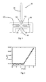
- Fig. 1 schematically illustrates a part of a first embodiment of a probe 10 having four cantilever arms designated the reference numeral 12 and a contact detector 14.
- the cantilever arms 12 and the contact detector 14 extend from the probe 10 over an edge 16 of a surface 18 of the probe 10.
- the contact detector may be used for detecting obstacles, deformations on or in the surface of the test sample, or simply detection of contact between the probe and the surface of the test sample.
- the cantilever arms 12 extend freely, and substantially parallel, from the edge 16.
- the contact detector 14 also extends freely from the edge 16.
- the contact detector shown is in the form of a cantilever structure with a flexible arm 21.
- the flexible arm 21 extends substantially parallel to the cantilever arms 12.
- the flexible arm 21 is attached to the probe 10 via the anchoring arms 20 and 22. These arms are coated with a conductive and non-piezoresistive metallic layer, so that they may function as a strain gauge sensor for detecting the deflection of the contact detector.
- the flexible arm 21 is electrically connected in a Wheatstone bridge circuit 24 used to detect changes in voltage/resistance as a result of the deflection of the flexible arm 21.
- the circuit 24 comprises three resistors with known resistance.
- the resistance of the strain gauge part established at the arms 20 and 22 of the flexible arm 21 is used as a measure for the deflection of the flexible arm 21.
- the strain gauge is established by a non-piezoresistive metal layer on a supporting silicon layer or structure.
- the silicon layer also constitutes the supporting body, i.e. the probe body 10.
- a coordinate system is established in Fig. 1 , with the z-axis parallel to the normal of the paper surface, the y-axis parallel to the flexible arm 21 and in the surface of the paper, and the x-axis perpendicular to the flexible arm 21 and in the surface of the paper. Assume that a force along the z-axis is acting on the tip of the flexible arm 48, which will cause the flexible arm 48 to deflect.
- the deflection will either compress or elongate the coating.
- the cross-section of the conducting metal will increase, while the length of the conducting path will decrease. Both of these effects will result in a decrease of resistance.
- the cross-section of the conducting metal will decrease, while the length of the conducting path will increase, which will lead to an increase of the resistance.
- the length of the first anchoring arm 20 will decrease, while the length of the second anchoring arm 22 will increase. At moderate deflections, both the changes in cross-section and the changes in length will counteract one another, resulting in an electrical resistance of the contact detector circuit 24 that, to a good approximation, remain unchanged.
- the anchoring arms 20 and 22 were of a piezoresistive material, due to the non-linearity of the resistance with respect to the applied force, the resistance of the contact detector circuit 24 would change significantly, even at moderate deflections of the flexible arm 21.
- a contact detector based on the principles put forward here should have the anchoring arms 20 and 22 of a non-piezoresistive material. It should also be noted that the contact detector in Fig. 1 is insensitive to a force component along the y-axis. This follows from that fact the flexible arm 21 will not, in this situation, work as a lever to create a length dependent moment at the base of the arm.
- the embodiment shown in the figures include a Wheatstone bridge near or at the contact structure, i.e. on top of the body of the probe 10.
- the circuit may be placed remotely, e.g. in a test apparatus or the like, or just at a different part of the probe 10.
- the contact detector 14 serves a supplementary purpose, namely as an error function. If the flexible arm 21 breaks off, the electrical path defined via the anchoring arms 20 and 22 will be disconnected and thus the resistance will increase to infinity, or at least very high.
- the electrical resistance of the strain gauge will change.
- the system will terminate the probe movement.
- the contact detector breaks at the anchoring arms 20 or 22 the resistance increases significantly in comparison to an almost balanced Wheatstone bridge. The system then aborts the measurement to prevent the probe to run into the surface.
- Fig. 2 schematically illustrates a second embodiment of a probe 10' having a plurality, i.e. four, cantilever arms 28, 30, 32, 34, where each arm includes an electrically conductive tip for establishing electrical contact with an area of a surface of a test sample.
- the probe 10' further includes two contact detectors 36 and 38.
- the contact detectors 36, 38 are of the same type as described with reference to Fig. 1 .
- Fig. 3 schematically illustrates a sketch of a strain gauge in a Wheatstone bridge configuration.
- the Wheatstone bridge is constituted by three resistors 42, 44 and 46 all with a non-variable resistance. The resistance may change with temperature, but it is not generally variable.
- the flexible arm 48 comprises a strain gauge element constituted by the metal layer constituting the electrical circuit.
- a current is applied between points 50 and 54.
- the output voltage between the points 52 and 56 is monitored continuously during engage, i.e. while the probe is in contact with the surface of the test sample.
- Vref a reference value is measured, defined as Vref.
- Vo an output voltage is measured between points 50 and 52, defined as Vo, when applying a current between points 54 and 56.
- Vout - Vref / Vo By continuously monitoring the relative change in the output voltage, given by: Vout - Vref / Vo is it possible to detect the contact point for the cantilever having the strain gauge element. This may be done as follows. Directly following that the probe is moved towards the surface, when the relative changes in the output voltage exceed a predefined value, the system will terminate the engage of the strain gauge. In case the cantilever of the strain gauge breaks the resistance will increase significantly in comparison to an almost balanced Wheatstone bridge. The system will then simply abort the measurement to prevent the probe to run into the surface.
- Fig. 4 schematically illustrates measured output voltage of a Wheatstone bridge as a function of the displacement of the strain sensor, i.e. surface detector, in one dimension, i.e. along the Z-axis.
- the current set-point is 500 ⁇ A.
- a constant output voltage is obtained.
- a force is exerted to the cantilever, which induces a strain in the sensor, consequently a change in the output voltage.
- a linear dependence of the z movement of the cantilever on the output voltage is observed, which is expected due to the use of non-piezoresistive materials in the circuitry.
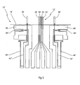
- Fig. 5 schematically illustrates a third embodiment of a probe 10".
- the third embodiment 10" of the probe differs from the above-described second embodiment shown in Fig. 2 in that the resistor, constituting a first branch of the Wheatstone bridge also including the contact detector is substituted by a replica of the contact detector itself.
- the contact detectors located at the left and right hand side of the cantilever arms 28', 30', 32' and 34' are designated the reference numerals 36' and 38' and the replica contact detectors connected in a series configuration with the contact detectors are designated the reference numerals 36" and 38".
- the two replica contact detectors 36" and 38" are located in respective recesses within the substrate, which recesses are designated the reference numerals 58 and 60, respectively, serving to protect the replica contact detectors 36" and 38" from being contacted with the surface of the test sample.
- the replica contact detectors consequently constitute reference detectors of the same resistance as the contact detectors consequently ensuring a high degree of accuracy, as the first branch of the Wheatstone bridge in each of the two Wheatstone bridges is constituted by identical resistive elements, one of which is a contact detector, which is exposed to mechanical bending for causing the anchoring arms of the contact detector to change their resistivity for detecting the establishing of contact between the contact detector and the surface of the test sample, as is readily described above.
- the Wheatstone bridges belonging to the two contact detectors 36' and 38' further comprise sets of reference resistors 42', 44' and 42", 44", respectively, constituting a second branch of the Wheatstone bridge of each of the two contact detectors 36' and 38'.
- the third embodiment shown in Fig. 5 basically provides the highly advantageous integration of identical resistors of the first branch of the Wheatstone bridges, as the contact detectors 36' and 38' are replicated into dummy resistors 36" and 38", respectively, firstly ensuring a high degree of identity between the properties of the measuring contact detector and the dummy contact detector of the two Wheatstone bridges and secondly provides a highly simple technique of producing the probe by simply replicating the contact detectors as identical reference detectors of the Wheatstone bridges.
Priority Applications (1)
| Application Number | Priority Date | Filing Date | Title |
|---|---|---|---|
| EP08388010A EP2101181A1 (de) | 2008-03-12 | 2008-03-12 | Vorrichtung mit Kontaktdetektor |
Applications Claiming Priority (1)
| Application Number | Priority Date | Filing Date | Title |
|---|---|---|---|
| EP08388010A EP2101181A1 (de) | 2008-03-12 | 2008-03-12 | Vorrichtung mit Kontaktdetektor |
Publications (1)
| Publication Number | Publication Date |
|---|---|
| EP2101181A1 true EP2101181A1 (de) | 2009-09-16 |
Family
ID=40001503
Family Applications (1)
| Application Number | Title | Priority Date | Filing Date |
|---|---|---|---|
| EP08388010A Withdrawn EP2101181A1 (de) | 2008-03-12 | 2008-03-12 | Vorrichtung mit Kontaktdetektor |
Country Status (1)
| Country | Link |
|---|---|
| EP (1) | EP2101181A1 (de) |
Cited By (3)
| Publication number | Priority date | Publication date | Assignee | Title |
|---|---|---|---|---|
| WO2012096416A1 (ko) * | 2011-01-10 | 2012-07-19 | 한국표준과학연구원 | 나노소재용 역학-전기 복합센서 |
| EP2677324A1 (de) | 2012-06-20 | 2013-12-25 | Capres A/S | Tiefgeätzte Mehrpunktsonde |
| CN112067928A (zh) * | 2020-09-09 | 2020-12-11 | 江苏普瑞德智能科技有限公司 | 一种供电系统监察装置 |
Citations (9)
| Publication number | Priority date | Publication date | Assignee | Title |
|---|---|---|---|---|
| US5266801A (en) | 1989-06-05 | 1993-11-30 | Digital Instruments, Inc. | Jumping probe microscope |
| US5907095A (en) | 1996-06-17 | 1999-05-25 | Industrial Technology Research Institute | High-sensitivity strain probe |
| US6148622A (en) | 1998-04-03 | 2000-11-21 | Alliedsignal Inc. | Environmental control system no condenser high pressure water separation system |
| US20020153909A1 (en) | 1998-07-08 | 2002-10-24 | Petersen Christian Leth | Nano-drive for high resolution positioning and for positioning of a multi-point probe |
| US6621080B2 (en) | 1998-01-22 | 2003-09-16 | Matsushita Electric Industrial Co., Ltd. | Apparatus for measuring a micro surface configuration and a method for manufacturing a probe incorporated in this measuring apparatus |
| US20040056674A1 (en) | 1998-07-08 | 2004-03-25 | Capres Aps | Multi-point probe |
| US6953519B2 (en) | 2002-08-30 | 2005-10-11 | Sii Nanotechnology Inc. | Method of manufacturing the multi-tip probe, a multi-tip probe, and surface characteristic analysis apparatus |
| WO2005124371A1 (en) | 2004-06-21 | 2005-12-29 | Capres A/S | A method for providing alignment of a probe |
| JP2006284599A (ja) | 2006-05-29 | 2006-10-19 | Sii Nanotechnology Inc | カンチレバーを用いて試料面の情報を取得する装置 |
-
2008
- 2008-03-12 EP EP08388010A patent/EP2101181A1/de not_active Withdrawn
Patent Citations (9)
| Publication number | Priority date | Publication date | Assignee | Title |
|---|---|---|---|---|
| US5266801A (en) | 1989-06-05 | 1993-11-30 | Digital Instruments, Inc. | Jumping probe microscope |
| US5907095A (en) | 1996-06-17 | 1999-05-25 | Industrial Technology Research Institute | High-sensitivity strain probe |
| US6621080B2 (en) | 1998-01-22 | 2003-09-16 | Matsushita Electric Industrial Co., Ltd. | Apparatus for measuring a micro surface configuration and a method for manufacturing a probe incorporated in this measuring apparatus |
| US6148622A (en) | 1998-04-03 | 2000-11-21 | Alliedsignal Inc. | Environmental control system no condenser high pressure water separation system |
| US20020153909A1 (en) | 1998-07-08 | 2002-10-24 | Petersen Christian Leth | Nano-drive for high resolution positioning and for positioning of a multi-point probe |
| US20040056674A1 (en) | 1998-07-08 | 2004-03-25 | Capres Aps | Multi-point probe |
| US6953519B2 (en) | 2002-08-30 | 2005-10-11 | Sii Nanotechnology Inc. | Method of manufacturing the multi-tip probe, a multi-tip probe, and surface characteristic analysis apparatus |
| WO2005124371A1 (en) | 2004-06-21 | 2005-12-29 | Capres A/S | A method for providing alignment of a probe |
| JP2006284599A (ja) | 2006-05-29 | 2006-10-19 | Sii Nanotechnology Inc | カンチレバーを用いて試料面の情報を取得する装置 |
Cited By (5)
| Publication number | Priority date | Publication date | Assignee | Title |
|---|---|---|---|---|
| WO2012096416A1 (ko) * | 2011-01-10 | 2012-07-19 | 한국표준과학연구원 | 나노소재용 역학-전기 복합센서 |
| US8621661B2 (en) | 2011-01-10 | 2013-12-31 | Korea Research Institute Of Standards And Science | Electrical-mechanical complex sensor for nanomaterials |
| EP2677324A1 (de) | 2012-06-20 | 2013-12-25 | Capres A/S | Tiefgeätzte Mehrpunktsonde |
| CN112067928A (zh) * | 2020-09-09 | 2020-12-11 | 江苏普瑞德智能科技有限公司 | 一种供电系统监察装置 |
| CN112067928B (zh) * | 2020-09-09 | 2023-02-28 | 江苏普瑞德智能科技有限公司 | 一种供电系统监察装置 |
Similar Documents
| Publication | Publication Date | Title |
|---|---|---|
| EP2132578B1 (de) | Einrichtung mit einem kontaktdetektor | |
| Wisitsoraat et al. | Low cost thin film based piezoresistive MEMS tactile sensor | |
| US7311009B2 (en) | Microelectromechanical systems contact stress sensor | |
| Cao et al. | Simulation and fabrication of piezoresistive membrane type MEMS strain sensors | |
| RU2498249C1 (ru) | Способ изготовления тензорезисторного датчика давления на основе тонкопленочной нано- и микроэлектромеханической системы | |
| Fung et al. | Fabrication of CNT-based MEMS piezoresistive pressure sensors using DEP nanoassembly | |
| EP2101181A1 (de) | Vorrichtung mit Kontaktdetektor | |
| WO2001014892A1 (en) | Beam strain gauge | |
| JP2006512589A (ja) | 縦および横の両方向のピエゾ抵抗係数を用いたカンチレバーセンサ | |
| JP2007078364A (ja) | ひずみ感知センサ | |
| RU2658089C1 (ru) | Датчик деформации | |
| Tibrewala et al. | Development, fabrication and characterization of a 3D tactile sensor | |
| JP5192095B2 (ja) | ひずみ感知センサ | |
| US9063036B2 (en) | Sample for electron microscopy and method of manufacturing the same | |
| US7752927B2 (en) | Cable-type load sensor | |
| Anderson et al. | Piezoresistive sensing of bistable micro mechanism state | |
| WO2004079292A2 (en) | Mems sensor for detecting stress corrosion cracking | |
| WO2014036010A1 (en) | Shear displacement extensometer | |
| Metz et al. | New parallelogram 3D-displacement sensor for micro probing and dimensional metrology | |
| Cao et al. | Calibration technique for MEMS membrane type strain sensors | |
| Sharma et al. | Review of MEMS test structures for mechanical parameter extraction | |
| Gnerlich et al. | A submersible piezoresistive MEMS lateral force sensor for cellular biomechanics applications | |
| Vallin et al. | High-temperature piezoresistive gauge fabricated on commercially available silicon-on-insulator wafers | |
| Spinner et al. | Electromechanical reliability testing of three-axial silicon force sensors | |
| SU1682834A1 (ru) | Способ определени остаточных напр жений |
Legal Events
| Date | Code | Title | Description |
|---|---|---|---|
| PUAI | Public reference made under article 153(3) epc to a published international application that has entered the european phase |
Free format text: ORIGINAL CODE: 0009012 |
|
| AK | Designated contracting states |
Kind code of ref document: A1 Designated state(s): AT BE BG CH CY CZ DE DK EE ES FI FR GB GR HR HU IE IS IT LI LT LU LV MC MT NL NO PL PT RO SE SI SK TR |
|
| AX | Request for extension of the european patent |
Extension state: AL BA MK RS |
|
| AKX | Designation fees paid | ||
| REG | Reference to a national code |
Ref country code: DE Ref legal event code: 8566 |
|
| STAA | Information on the status of an ep patent application or granted ep patent |
Free format text: STATUS: THE APPLICATION IS DEEMED TO BE WITHDRAWN |
|
| 18D | Application deemed to be withdrawn |
Effective date: 20100317 |