EP2099130A1 - Surface acoustic wave filter device - Google Patents
Surface acoustic wave filter device Download PDFInfo
- Publication number
- EP2099130A1 EP2099130A1 EP07829183A EP07829183A EP2099130A1 EP 2099130 A1 EP2099130 A1 EP 2099130A1 EP 07829183 A EP07829183 A EP 07829183A EP 07829183 A EP07829183 A EP 07829183A EP 2099130 A1 EP2099130 A1 EP 2099130A1
- Authority
- EP
- European Patent Office
- Prior art keywords
- acoustic wave
- surface acoustic
- wave filter
- idt
- coupled resonator
- Prior art date
- Legal status (The legal status is an assumption and is not a legal conclusion. Google has not performed a legal analysis and makes no representation as to the accuracy of the status listed.)
- Withdrawn
Links
- 238000010897 surface acoustic wave method Methods 0.000 title claims abstract description 95
- 239000000758 substrate Substances 0.000 claims abstract description 26
- 239000003990 capacitor Substances 0.000 claims abstract description 19
- 230000001902 propagating effect Effects 0.000 claims description 12
- 229910012463 LiTaO3 Inorganic materials 0.000 description 4
- 229910052751 metal Inorganic materials 0.000 description 3
- 239000002184 metal Substances 0.000 description 3
- 229910003327 LiNbO3 Inorganic materials 0.000 description 1
- 229910045601 alloy Inorganic materials 0.000 description 1
- 239000000956 alloy Substances 0.000 description 1
- 230000015572 biosynthetic process Effects 0.000 description 1
- 230000001413 cellular effect Effects 0.000 description 1
- 239000000919 ceramic Substances 0.000 description 1
- 230000000052 comparative effect Effects 0.000 description 1
- 239000013078 crystal Substances 0.000 description 1
- 230000002708 enhancing effect Effects 0.000 description 1
- 230000001747 exhibiting effect Effects 0.000 description 1
- 239000000463 material Substances 0.000 description 1
- 150000002739 metals Chemical class 0.000 description 1
- 230000004048 modification Effects 0.000 description 1
- 238000012986 modification Methods 0.000 description 1
- 239000010453 quartz Substances 0.000 description 1
- VYPSYNLAJGMNEJ-UHFFFAOYSA-N silicon dioxide Inorganic materials O=[Si]=O VYPSYNLAJGMNEJ-UHFFFAOYSA-N 0.000 description 1
Images


Classifications
-
- H—ELECTRICITY
- H03—ELECTRONIC CIRCUITRY
- H03H—IMPEDANCE NETWORKS, e.g. RESONANT CIRCUITS; RESONATORS
- H03H9/00—Networks comprising electromechanical or electro-acoustic elements; Electromechanical resonators
- H03H9/46—Filters
- H03H9/64—Filters using surface acoustic waves
- H03H9/6423—Means for obtaining a particular transfer characteristic
- H03H9/6433—Coupled resonator filters
- H03H9/644—Coupled resonator filters having two acoustic tracks
- H03H9/6456—Coupled resonator filters having two acoustic tracks being electrically coupled
- H03H9/6469—Coupled resonator filters having two acoustic tracks being electrically coupled via two connecting electrodes
- H03H9/6476—Coupled resonator filters having two acoustic tracks being electrically coupled via two connecting electrodes the tracks being electrically parallel
Definitions
- the present invention relates to longitudinally coupled resonator-type surface acoustic wave filter devices, and more particularly to a surface acoustic wave filter device including a first and a second longitudinally coupled resonator-type surface acoustic wave filter that are connected in a cascade arrangement on a piezoelectric substrate.
- a longitudinally coupled resonator-type surface acoustic wave filter device is widely used as the RF stage band-pass filter of cellular phones.
- a structure is often employed in which a plurality of longitudinally coupled resonator-type surface acoustic wave filters are connected in a cascade arrangement.
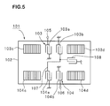
- Patent Document 1 discloses a two-stage cascaded longitudinally coupled resonator-type surface acoustic wave filter device as shown in Fig. 5 .
- the longitudinally coupled resonator-type surface acoustic wave filter device 101 shown in Fig. 5 has an electrode structure schematically shown in Fig. 5 on a piezoelectric substrate 102.
- the piezoelectric substrate 102 is made of a 36° Y-cut X-propagating LiTaO 3 .
- a first longitudinally coupled resonator-type surface acoustic wave filter 103 and a second longitudinally coupled resonator-type surface acoustic wave filter 104 are connected in a cascade arrangement on the piezoelectric substrate 102.
- the longitudinally coupled resonator-type surface acoustic wave filter 103 includes a first and a second IDT 103a and 103b disposed with a distance therebetween in the surface acoustic wave propagating direction. Reflectors 103c and 103d are disposed at the sides of the IDTs 103a and 103b in the surface wave propagating direction.
- the second longitudinally coupled resonator-type surface acoustic wave filer 104 also includes a first and a second IDT 104a and 104b, and reflectors 104c and 104d disposed at the sides of the IDTs 104a and 104b in the surface wave propagating direction.
- One end of the first IDT 103a of the first longitudinally coupled resonator-type surface acoustic wave filter 103 is connected to an input terminal 105 and the other end is connected to the ground potential.
- One end of the second IDT 103b is connected to the ground potential and the other end is connected to the first IDT 104a of the second longitudinally coupled resonator-type surface acoustic wave filter 104 with a signal line 107.
- One end of the IDT 104a is connected to the signal line 107 and the other end is connected to the ground potential.
- One end of the second IDT 104b of the second longitudinally coupled resonator-type surface acoustic wave filter 104 is connected to the ground potential and the other end is connected to an output terminal 106.
- a comb-like electrode 108 is connected between the signal line 107 and the ground potential.
- the comb-like electrode 108 is intended to provide a capacitance between the signal line 107 for inter-stage connection and the ground potential, thereby suppressing spurious responses in the pass band.
- a relatively large comb-like electrode 108 is required. This often restricts the electrode structure of the surface acoustic wave filters 103 and 104 on the piezoelectric substrate 102, and the formation area of the wirings with connection to the signal line 107 and the ground potential.
- the surface acoustic wave filter device must be large, and this hinders miniaturization. Since the layout of the electrodes and wires are restricted, it is difficult to improve the performance by the modification of the layout.
- a purpose of the invention is to provide a longitudinally coupled resonator-type surface acoustic wave filter device having a structure allowing the miniaturization and the reduction of spurious responses within the pass band, and enhancing the design flexibility of the electrode structure and the wiring layout on the piezoelectric substrate.
- the preset invention provides a surface acoustic wave filter device including a piezoelectric substrate and a first and a second longitudinally coupled resonator-type surface acoustic wave filter disposed on the piezoelectric substrate.
- Each longitudinally coupled resonator-type surface acoustic wave filter includes a first IDT, a second and a third IDT respectively disposed to both sides of the first IDT in the surface acoustic wave propagating direction, and a pair of reflectors disposed at both sides in the surface wave propagating direction of the area on which the first to third IDTs are disposed.
- a first signal line is disposed to connect a signal terminal of the second IDT of the first longitudinally coupled resonator-type surface acoustic wave filter and a signal terminal of the second IDT of the second longitudinally coupled resonator-type surface acoustic wave filter to each other.
- a second signal line is disposed to connect a signal terminal of the third IDT of the first longitudinally coupled resonator-type surface acoustic wave filter and a signal terminal of the third IDT of the second longitudinally coupled resonator-type surface acoustic wave filter to each other.
- at least one capacitor is connected between the first and the second signal line. The phase of the electrical signal transmitted through the first signal line is 180° different from the phase of the electrical signal transmitted through the second signal line.
- the capacitor is a comb-like electrode formed on the piezoelectric substrate.
- the comb-like electrode is small, but can provide a large capacitance. Accordingly, the surface acoustic wave filter device can be miniaturized.
- the first IDTs of the first and the second longitudinally coupled resonator-type surface acoustic wave filter are connected to a first and a second unbalanced signal terminal, respectively.
- This structure provides a small unbalanced input/output band-pass filter not affected by spurious responses within the pass band, exhibiting superior characteristics.
- a first and a second longitudinally coupled resonator-type surface acoustic wave filter each having first to third IDTs are connected in a cascade arrangement by connecting the signal terminals of their second IDTs to each other with a first signal line, and connecting the signal terminals of their third IDTs to each other with a second signal line.
- at least one capacitor is connected between the first and the second signal line to provide a capacitance between stages.
- spurious responses in the pass band are reduced.
- an inter-stage capacitor is connected between a signal line and the ground potential. Consequently, a large comb-like electrode must be disposed to sufficiently reduce spurious responses.
- the capacitor is disposed between the first and the second signal line. This arrangement can reduce the size of the capacitor required to sufficiently reduce spurious responses.
- the surface acoustic wave filter device can be miniaturized and the design flexibility of the layout of the electrodes and wiring lines on the piezoelectric substrate can be enhanced. Accordingly, the performance can be enhanced by modifying the layout of the electrodes and the wiring lines, and thereby, a small, high-performance surface acoustic wave filter can be provided.
- Fig. 1 is a schematic plan view a surface acoustic wave filter device according to a first embodiment of the invention.
- the surface acoustic wave filter device 1 includes a piezoelectric substrate 2.
- the piezoelectric substrate 2 is made of LiTaO 3 in the present embodiment.
- the piezoelectric substrate 2, however, may be a LiTaO 3 substrate having a different cut angle, or may be made of other piezoelectric single crystal, such as LiNbO 3 or quartz, or piezoelectric ceramic.
- An electrode structure and wiring lines which are schematically shown in the figure, are formed on the piezoelectric substrate 2.
- a first longitudinally coupled resonator-type surface acoustic wave filter 3 and a second longitudinally coupled resonator-type surface acoustic wave filter 4 are disposed on the piezoelectric substrate 2.
- the first longitudinally coupled resonator-type surface acoustic wave filter 3 includes a first IDT 3a, and a second and a third IDT 3b and 3c respectively disposed at both sides of the first IDT 3a in the surface wave propagating direction.
- reflectors 3d and 3e are disposed at both sides in the surface wave propagating direction of the area to which the first to third IDTs 3a to 3c are disposed.
- the second longitudinally coupled resonator-type surface acoustic wave filter 4 also includes a first IDT 4a, and a second and a third IDT 4b and 4c respectively disposed at both sides of the first IDT 4a in the surface wave propagating direction. Also, reflectors 4d and 4e are disposed at both sides in the surface wave propagating direction of the area in which the IDTs 4a to 4c are disposed.
- One end of the first IDT 3a is connected to a first unbalanced terminal 5 that is one of input/output terminals.
- the other end of the IDT 3a is connected to a ground line 7.
- the ground line 7 connects the IDT 3a to the reflector 3e, and the reflector 3e is connected to the ground potential. Hence, that other end of the IDT 3a is connected to the ground potential.
- the ground line 7 is also connected to the reflector 4e, and the reflector 4e is thus connected to the ground potential.
- One end of the second IDT 3b is connected to the ground potential, and the other end is connected to a first signal line 9. That other end of the second IDT 3b and one end of the second IDT 4b of the second longitudinally coupled resonator-type surface acoustic wave filter 4 are connected to each other with the first signal line 9. The other end of the second IDT 4b is connected to the ground potential. In other words, the signal terminal of the second IDT 3b and the signal terminal of the second IDT 4b are electrically connected to each other with the first signal line 9.
- one end of the third IDT 3c is connected to the ground potential, and the other end, or signal terminal, is connected to a second signal line 10.
- the second signal line 10 is connected to one end, or signal terminal, of the third IDT 4c.
- the other end of the third IDT 4c is connected to the ground potential.
- One end of the first IDT 4a is connected to a second unbalanced terminal 6 that is the other of the input/output terminals, and the other end is connected to a ground line 8.
- the ground line 8 is electrically connected to that other end of the IDT 4a, and the reflectors 3d and 4d.
- the reflector 4d is connected to the ground potential.
- the terminal of the IDT 4a opposite to the end connected to the unbalanced terminal 6 is connected to the ground potential.
- the phase of the signal transmitted through the first signal line 9 is 180° different from that of the signal transmitted through the second signal line.
- the first signal line 9 and the second signal line 10 are balanced signal lines.
- the first IDTs 3a and 4a each have an even number of electrode fingers
- the second and the third IDTs 3b, 3c, 4b and 4c each have an odd number of electrode fingers.
- the surface acoustic wave filter device 1 has an unbalanced input-unbalanced output structure.
- the first to third IDTs 3a, 4a, 3b, 3c, 4b and 4c each may have an even number of electrode fingers with the second IDTs 3b and 4b disposed in opposite orientation to the third IDTs 3c and 4c.
- the feature of the surface acoustic wave filter device 1 of the present embodiment is that a capacitor defined by a comb-like electrode 11 is connected between the first and the second signal line 9 and 10.
- a capacitor defined by a comb-like electrode 11 is connected between the first and the second signal line 9 and 10.
- the structure in which the comb-like electrode 11 provides a capacitance can suppress spurious responses to the same extent as the known surface acoustic wave filter device 101 even though the capacitor is smaller than the comb-like electrode 108 of the known surface acoustic wave filter device 101. Since the performance can be improved with a smaller comb-like electrode 11, the surface acoustic wave filter device 1 can be miniaturized.
- the electrode structure of the longitudinally coupled resonator-type surface acoustic wave filters 3 and 4, and the layout of the signal lines 9 and 10, the ground lines 7 and 8, and the wiring for connecting the IDTs 3b, 3c, 4b and 4c and the reflectors 3e and 4d to the ground potential can be more flexibly designed on the piezoelectric substrate 2. Accordingly, the performance of the filter device can easily be improved by modifying the electrode structure or the wiring layout.
- the material of the electrode structure and the wiring lines can be arbitrarily selected from metals and alloys as desired without particular limitation.
- the electrode structure or the wiring lines may be made of a multilayer metal film including a plurality of metal layers.
- the surface acoustic wave filter device 1 of the present embodiment with a smaller capacitor can enhance the performance, with reference to a specific experimental example.
- a surface acoustic wave filter device 1 was prepared according to the following specifications.
- the overlap of the IDTs 3a to 3c and 4a to 4c was set at 19 ⁇ , where ⁇ represents the wavelength determined by the pitch of the electrode fingers of the IDTs 3a to 3c.
- the duty ratios of the IDTs 3a to 3c and 4a to 4c and the reflectors 3d, 3e, 4d and 4e were each set at 0.55.
- the thickness of the electrodes of the IDT and the reflector was set at 0.03 ⁇ .
- Capacitance of the comb-like electrode 11 2.5 pF
- the middle IDT, or first IDT had 25.5 pairs of electrode fingers, that is, an even number of, 52, electrode fingers, and the outer IDTs, or the second and the third IDT 3b, 3c, 4b and 4c, each have an odd number of, 31, electrode fingers.
- the piezoelectric substrate 2 was made of LiTaO 3 , and the electrodes and the wiring pattern were made of Al.
- Fig. 4 shows attenuation/frequency characteristics in the frequency range of 0 to 1500 MHz.
- Fig. 3 shows part of the attenuation/frequency characteristics in the range of 290 to 340 MHz, and further shows the main portion of the pass band in an enlarged scale using the right axis.
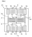
- a surface acoustic wave filter device 51 shown in Fig. 2 was prepared.
- This surface acoustic wave filter device 51 has the same structure as the above-described surface acoustic wave filter device 1, except for the connection between the longitudinally coupled resonator-type surface acoustic wave filters 3 and 4 and the electrode defining the inter-stage capacitor. More specifically, one ends of the second and the third IDT 3b and 3c of the first longitudinally coupled resonator-type surface acoustic wave filter 3 are connected together to a signal line 52, as shown in Fig. 2 .
- one ends of the second and the third IDT 4b and 4c of the second longitudinally coupled resonator-type surface acoustic wave filter 4 are connected together to the signal line 52.
- the signal line 52 connects the first and the second longitudinally coupled resonator-type surface acoustic wave filter 3 and 4.
- comb-like electrodes 53 and 54 are connected between the signal line 52 and the ground lines 7 and 8.
- the comb-like electrodes 53 and 54 are each connected between a signal line and the ground potential between the stages.
- the overlap of the electrode fingers of the comb-like electrodes 53 and 54 and the number of pairs of the electrode fingers were adjusted so as to control the spurious responses in the pass band as in the above example, that is, so as to have the same filter characteristics.
- the comb-like electrodes 53 and 54 each had 12 pairs of electrode fingers with an overlap of 660 ⁇ m, the characteristics indicated by broken lines in Figs. 3 and 4 were obtained.
- the filter characteristics indicated by solid lines and broken lines shown in Figs. 3 and 4 are substantially the same and do not show large spurious responses in the pass band.
- the comb-like electrodes 53 and 54 of the surface acoustic wave filter device 51 of the comparative example occupies a large area of 92400 ⁇ m 2
- the comb-like electrode 11 of the surface acoustic wave filter device 1 of the example occupies an area of 23100 ⁇ m 2 .
- the embodiment of the invention not only allows the inter-stage capacitor to reduce spurious responses in the pass band, but also allows the miniaturization of the comb-like electrode 11 defining the inter-stage capacitor, thus miniaturizing the surface acoustic wave filter device 11.
- the area of the region where the comb-like electrode 11 is disposed can be reduced, for example, an electrode pad connected to the ground potential can be provided around the comb-like electrode 11. Accordingly, the design flexibility of the layout of the electrodes including the electrode pad and the wiring lines is increased, and thus the characteristics outside the pass band can be improved.
- the comb-like electrode 11 defines an inter-stage capacitor
- other structures may provide a capacitance between the stages.
- Structures used as the inter-stage capacitor may be such that linear electrodes oppose each other with a predetermined distance on the piezoelectric substrate 2, or such that a pair of electrodes is separated by a dielectric layer formed on the piezoelectric substrate 2.
- the structure using the comb-like electrode 11 can provide a sufficient capacitance using a small area, and is thus most preferable for further miniaturization.
- While the above embodiment describes a two-stage cascaded surface acoustic wave filter device in which the first and the second longitudinally coupled resonator-type surface acoustic wave filter 3 and 4 are connected in a cascade arrangement, the present invention can be applied to surface acoustic wave filter devices having three or more stages.
- the longitudinally coupled resonator-type surface acoustic wave filter may have five IDTs including a fourth and a fifth IDT disposed at both sides of, for example, the second and third IDTs in the surface wave propagating direction, instead of the three-IDT type having the first to third IDTs.
- one ends of the fourth and the fifth IDT can be connected together to the terminal of the first IDT connected to an unbalanced terminal, and the other ends can be connected to the ground potential.
Landscapes
- Physics & Mathematics (AREA)
- Acoustics & Sound (AREA)
- Surface Acoustic Wave Elements And Circuit Networks Thereof (AREA)
Abstract
A cascaded longitudinally coupled resonator-type surface acoustic wave filter device including an inter-stage capacitor is miniaturized. A first and a second longitudinally coupled resonator-type surface acoustic wave filter (3 and 4) are disposed on a piezoelectric substrate (2). One end of a first IDT (3a) arranged at the middle of the first longitudinally coupled resonator-type surface acoustic wave filter is connected to a first unbalanced terminal (5), and one end of a first IDT (4a) arranged at the middle of the second longitudinally coupled resonator-type surface acoustic wave filter is connected to a second unbalanced terminal (6). Signal terminals of second IDTs (3b and 4b) of the first and the second longitudinally coupled resonator-type surface acoustic wave filter (3 and 4) are connected to each other with a first signal line (9). Third IDTs (3c and 4c) are connected to each other with a second signal line (10). A capacitor (11) is connected between the first and the second signal line (9 and 10).
Description
- The present invention relates to longitudinally coupled resonator-type surface acoustic wave filter devices, and more particularly to a surface acoustic wave filter device including a first and a second longitudinally coupled resonator-type surface acoustic wave filter that are connected in a cascade arrangement on a piezoelectric substrate.
- In general, a longitudinally coupled resonator-type surface acoustic wave filter device is widely used as the RF stage band-pass filter of cellular phones. When a large attenuation is required outside the pass band for a longitudinally coupled resonator-type surface acoustic wave filter device, a structure is often employed in which a plurality of longitudinally coupled resonator-type surface acoustic wave filters are connected in a cascade arrangement.
- For example, the below listed
Patent Document 1 discloses a two-stage cascaded longitudinally coupled resonator-type surface acoustic wave filter device as shown inFig. 5 . - The longitudinally coupled resonator-type surface acoustic
wave filter device 101 shown inFig. 5 has an electrode structure schematically shown inFig. 5 on apiezoelectric substrate 102. Thepiezoelectric substrate 102 is made of a 36° Y-cut X-propagating LiTaO3. A first longitudinally coupled resonator-type surfaceacoustic wave filter 103 and a second longitudinally coupled resonator-type surfaceacoustic wave filter 104 are connected in a cascade arrangement on thepiezoelectric substrate 102. The longitudinally coupled resonator-type surfaceacoustic wave filter 103 includes a first and a second IDT 103a and 103b disposed with a distance therebetween in the surface acoustic wave propagating direction.Reflectors acoustic wave filer 104 also includes a first and asecond IDT 104a and 104b, andreflectors 104c and 104d disposed at the sides of theIDTs 104a and 104b in the surface wave propagating direction. - One end of the first IDT 103a of the first longitudinally coupled resonator-type surface
acoustic wave filter 103 is connected to aninput terminal 105 and the other end is connected to the ground potential. One end of the second IDT 103b is connected to the ground potential and the other end is connected to the first IDT 104a of the second longitudinally coupled resonator-type surfaceacoustic wave filter 104 with asignal line 107. One end of the IDT 104a is connected to thesignal line 107 and the other end is connected to the ground potential. One end of the second IDT 104b of the second longitudinally coupled resonator-type surfaceacoustic wave filter 104 is connected to the ground potential and the other end is connected to anoutput terminal 106. - In the longitudinally coupled resonator-type surface acoustic
wave filter device 101, a comb-like electrode 108 is connected between thesignal line 107 and the ground potential. According toPatent Document 1, the comb-like electrode 108 is intended to provide a capacitance between thesignal line 107 for inter-stage connection and the ground potential, thereby suppressing spurious responses in the pass band. - Patent Document 1: Japanese Unexamined Patent Application Publication
7-74588 - In order to provide a capacitance sufficient to reduce spurious responses in the longitudinally coupled resonator-type surface acoustic
wave filter device 101, however, a relatively large comb-like electrode 108 is required. This often restricts the electrode structure of the surfaceacoustic wave filters piezoelectric substrate 102, and the formation area of the wirings with connection to thesignal line 107 and the ground potential. - Accordingly, the surface acoustic wave filter device must be large, and this hinders miniaturization. Since the layout of the electrodes and wires are restricted, it is difficult to improve the performance by the modification of the layout.
- Accordingly, a purpose of the invention is to provide a longitudinally coupled resonator-type surface acoustic wave filter device having a structure allowing the miniaturization and the reduction of spurious responses within the pass band, and enhancing the design flexibility of the electrode structure and the wiring layout on the piezoelectric substrate.
- The preset invention provides a surface acoustic wave filter device including a piezoelectric substrate and a first and a second longitudinally coupled resonator-type surface acoustic wave filter disposed on the piezoelectric substrate. Each longitudinally coupled resonator-type surface acoustic wave filter includes a first IDT, a second and a third IDT respectively disposed to both sides of the first IDT in the surface acoustic wave propagating direction, and a pair of reflectors disposed at both sides in the surface wave propagating direction of the area on which the first to third IDTs are disposed. A first signal line is disposed to connect a signal terminal of the second IDT of the first longitudinally coupled resonator-type surface acoustic wave filter and a signal terminal of the second IDT of the second longitudinally coupled resonator-type surface acoustic wave filter to each other. A second signal line is disposed to connect a signal terminal of the third IDT of the first longitudinally coupled resonator-type surface acoustic wave filter and a signal terminal of the third IDT of the second longitudinally coupled resonator-type surface acoustic wave filter to each other. In addition, at least one capacitor is connected between the first and the second signal line. The phase of the electrical signal transmitted through the first signal line is 180° different from the phase of the electrical signal transmitted through the second signal line.
- Preferably, the capacitor is a comb-like electrode formed on the piezoelectric substrate. The comb-like electrode is small, but can provide a large capacitance. Accordingly, the surface acoustic wave filter device can be miniaturized.
- Preferably, the first IDTs of the first and the second longitudinally coupled resonator-type surface acoustic wave filter are connected to a first and a second unbalanced signal terminal, respectively. This structure provides a small unbalanced input/output band-pass filter not affected by spurious responses within the pass band, exhibiting superior characteristics.
- In the surface acoustic wave filter device of the present invention, a first and a second longitudinally coupled resonator-type surface acoustic wave filter each having first to third IDTs are connected in a cascade arrangement by connecting the signal terminals of their second IDTs to each other with a first signal line, and connecting the signal terminals of their third IDTs to each other with a second signal line. In addition, at least one capacitor is connected between the first and the second signal line to provide a capacitance between stages. Thus, spurious responses in the pass band are reduced. In the surface acoustic wave filter device disclosed in
Patent Document 1, an inter-stage capacitor is connected between a signal line and the ground potential. Consequently, a large comb-like electrode must be disposed to sufficiently reduce spurious responses. On the other hand, in the present invention, the capacitor is disposed between the first and the second signal line. This arrangement can reduce the size of the capacitor required to sufficiently reduce spurious responses. - Since a smaller capacitor can improve the performance of the filter, the surface acoustic wave filter device can be miniaturized and the design flexibility of the layout of the electrodes and wiring lines on the piezoelectric substrate can be enhanced. Accordingly, the performance can be enhanced by modifying the layout of the electrodes and the wiring lines, and thereby, a small, high-performance surface acoustic wave filter can be provided.
-
- [
Fig. 1] Fig. 1 is a schematic plan view of a surface acoustic wave filter device according to an embodiment of the invention. - [
Fig. 2] Fig. 2 is a schematic plan view of a surface acoustic wave filter device prepared for comparison. - [
Fig. 3] Fig. 3 is a representation of attenuation/frequency characteristics of a surface acoustic wave filter device of the embodiment shown inFig. 1 and the surface acoustic wave filter device prepared for comparison. - [
Fig. 4] Fig. 4 shows attenuation/frequency characteristics of the surface acoustic wave filter devices of the embodiment shown inFig. 1 and prepared for comparison. - [
Fig. 5] Fig. 5 is a schematic plan view of a known surface acoustic wave filter device. -
- 1
- surface acoustic wave filter device
- 2
- piezoelectric substrate
- 3
- first longitudinally coupled resonator-type surface acoustic wave filter
- 3a-3c
- first to third IDT
- 3d, 3e
- reflector
- 4
- second longitudinally coupled resonator-type surface acoustic wave filter
- 4a-4c
- first to third IDT
- 4d, 4e
- reflector
- 5
- first unbalanced terminal
- 6
- second unbalanced terminal
- 7, 8
- ground line
- 9, 10
- first/second signal line
- 11
- comb-like electrode
- The present invention will further be described in detail below, using a specific embodiment with reference to the drawings.
-
Fig. 1 is a schematic plan view a surface acoustic wave filter device according to a first embodiment of the invention. - The surface acoustic
wave filter device 1 includes apiezoelectric substrate 2. Thepiezoelectric substrate 2 is made of LiTaO3 in the present embodiment. Thepiezoelectric substrate 2, however, may be a LiTaO3 substrate having a different cut angle, or may be made of other piezoelectric single crystal, such as LiNbO3 or quartz, or piezoelectric ceramic. - An electrode structure and wiring lines, which are schematically shown in the figure, are formed on the
piezoelectric substrate 2. - More specifically, a first longitudinally coupled resonator-type surface
acoustic wave filter 3 and a second longitudinally coupled resonator-type surfaceacoustic wave filter 4 are disposed on thepiezoelectric substrate 2. The first longitudinally coupled resonator-type surfaceacoustic wave filter 3 includes afirst IDT 3a, and a second and athird IDT first IDT 3a in the surface wave propagating direction. Also,reflectors - The second longitudinally coupled resonator-type surface
acoustic wave filter 4 also includes afirst IDT 4a, and a second and athird IDT 4b and 4c respectively disposed at both sides of thefirst IDT 4a in the surface wave propagating direction. Also,reflectors IDTs 4a to 4c are disposed. One end of thefirst IDT 3a is connected to a firstunbalanced terminal 5 that is one of input/output terminals. The other end of theIDT 3a is connected to aground line 7. Theground line 7 connects theIDT 3a to thereflector 3e, and thereflector 3e is connected to the ground potential. Hence, that other end of theIDT 3a is connected to the ground potential. - The
ground line 7 is also connected to thereflector 4e, and thereflector 4e is thus connected to the ground potential. - One end of the
second IDT 3b is connected to the ground potential, and the other end is connected to afirst signal line 9. That other end of thesecond IDT 3b and one end of thesecond IDT 4b of the second longitudinally coupled resonator-type surfaceacoustic wave filter 4 are connected to each other with thefirst signal line 9. The other end of thesecond IDT 4b is connected to the ground potential. In other words, the signal terminal of thesecond IDT 3b and the signal terminal of thesecond IDT 4b are electrically connected to each other with thefirst signal line 9. - Similarly, one end of the
third IDT 3c is connected to the ground potential, and the other end, or signal terminal, is connected to asecond signal line 10. Thesecond signal line 10 is connected to one end, or signal terminal, of the third IDT 4c. The other end of the third IDT 4c is connected to the ground potential. One end of thefirst IDT 4a is connected to a secondunbalanced terminal 6 that is the other of the input/output terminals, and the other end is connected to aground line 8. Theground line 8 is electrically connected to that other end of theIDT 4a, and thereflectors reflector 4d is connected to the ground potential. Hence, the terminal of theIDT 4a opposite to the end connected to theunbalanced terminal 6 is connected to the ground potential. - The phase of the signal transmitted through the
first signal line 9 is 180° different from that of the signal transmitted through the second signal line. Hence, thefirst signal line 9 and thesecond signal line 10 are balanced signal lines. However, thefirst IDTs third IDTs wave filter device 1 has an unbalanced input-unbalanced output structure. - As long as the first and the
second signal line third IDTs second IDTs third IDTs 3c and 4c. - The feature of the surface acoustic
wave filter device 1 of the present embodiment is that a capacitor defined by a comb-like electrode 11 is connected between the first and thesecond signal line acoustic wave filter like electrode 11 providing a capacitance between stages. - In addition, the structure in which the comb-
like electrode 11 provides a capacitance can suppress spurious responses to the same extent as the known surface acousticwave filter device 101 even though the capacitor is smaller than the comb-like electrode 108 of the known surface acousticwave filter device 101. Since the performance can be improved with a smaller comb-like electrode 11, the surface acousticwave filter device 1 can be miniaturized. Since the comb-like electrode 11 can be miniaturized, the electrode structure of the longitudinally coupled resonator-type surfaceacoustic wave filters signal lines ground lines IDTs reflectors piezoelectric substrate 2. Accordingly, the performance of the filter device can easily be improved by modifying the electrode structure or the wiring layout. - The material of the electrode structure and the wiring lines can be arbitrarily selected from metals and alloys as desired without particular limitation. The electrode structure or the wiring lines may be made of a multilayer metal film including a plurality of metal layers.
- It will now be shown that the surface acoustic
wave filter device 1 of the present embodiment with a smaller capacitor can enhance the performance, with reference to a specific experimental example. - A surface acoustic
wave filter device 1 was prepared according to the following specifications. - Number of pairs of the electrode fingers of the
first IDTs
Number of pairs of the electrode fingers of the second and thethird IDTs
Number of electrode fingers of thereflectors
The overlap of theIDTs 3a to 3c and 4a to 4c was set at 19λ, where λ represents the wavelength determined by the pitch of the electrode fingers of theIDTs 3a to 3c. The duty ratios of theIDTs 3a to 3c and 4a to 4c and thereflectors - Capacitance of the comb-like electrode 11: 2.5 pF
The comb-like electrode 11 has 12 pairs of electrode fingers, and the overlap of the electrode fingers was 330 µm. In this instance, the comb-like electrode 11 occupied an area of 330 µm × 70 µm = 23100 µm2 on thepiezoelectric substrate 2. - In the present embodiment, in order to transmit balanced signals through the
signal lines third IDT - The
piezoelectric substrate 2 was made of LiTaO3, and the electrodes and the wiring pattern were made of Al. - The attenuation/frequency characteristic of the surface acoustic
wave filter device 1 prepared according to the above specifications was shown in solid line inFigs. 3 and 4. Fig. 4 shows attenuation/frequency characteristics in the frequency range of 0 to 1500 MHz.Fig. 3 shows part of the attenuation/frequency characteristics in the range of 290 to 340 MHz, and further shows the main portion of the pass band in an enlarged scale using the right axis. - For comparison, a surface acoustic
wave filter device 51 shown inFig. 2 was prepared. This surface acousticwave filter device 51 has the same structure as the above-described surface acousticwave filter device 1, except for the connection between the longitudinally coupled resonator-type surfaceacoustic wave filters third IDT acoustic wave filter 3 are connected together to asignal line 52, as shown inFig. 2 . Similarly, one ends of the second and thethird IDT 4b and 4c of the second longitudinally coupled resonator-type surfaceacoustic wave filter 4 are connected together to thesignal line 52. Thus, thesignal line 52 connects the first and the second longitudinally coupled resonator-type surfaceacoustic wave filter like electrodes signal line 52 and theground lines like electrodes - In the surface acoustic
wave filter device 51 shown inFig. 2 , the overlap of the electrode fingers of the comb-like electrodes like electrodes Figs. 3 and 4 were obtained. In this instance, the comb-like electrodes - The filter characteristics indicated by solid lines and broken lines shown in
Figs. 3 and 4 are substantially the same and do not show large spurious responses in the pass band. However, the comb-like electrodes wave filter device 51 of the comparative example occupies a large area of 92400 µm2, while the comb-like electrode 11 of the surface acousticwave filter device 1 of the example occupies an area of 23100 µm2. Thus, the embodiment of the invention not only allows the inter-stage capacitor to reduce spurious responses in the pass band, but also allows the miniaturization of the comb-like electrode 11 defining the inter-stage capacitor, thus miniaturizing the surface acousticwave filter device 11. - Since the area of the region where the comb-
like electrode 11 is disposed can be reduced, for example, an electrode pad connected to the ground potential can be provided around the comb-like electrode 11. Accordingly, the design flexibility of the layout of the electrodes including the electrode pad and the wiring lines is increased, and thus the characteristics outside the pass band can be improved. - While in the surface acoustic
wave filter device 1 of the above embodiment, the comb-like electrode 11 defines an inter-stage capacitor, other structures may provide a capacitance between the stages. Structures used as the inter-stage capacitor may be such that linear electrodes oppose each other with a predetermined distance on thepiezoelectric substrate 2, or such that a pair of electrodes is separated by a dielectric layer formed on thepiezoelectric substrate 2. However, the structure using the comb-like electrode 11 can provide a sufficient capacitance using a small area, and is thus most preferable for further miniaturization. - While the above embodiment describes a two-stage cascaded surface acoustic wave filter device in which the first and the second longitudinally coupled resonator-type surface
acoustic wave filter - The longitudinally coupled resonator-type surface acoustic wave filter may have five IDTs including a fourth and a fifth IDT disposed at both sides of, for example, the second and third IDTs in the surface wave propagating direction, instead of the three-IDT type having the first to third IDTs. In such a structure, one ends of the fourth and the fifth IDT can be connected together to the terminal of the first IDT connected to an unbalanced terminal, and the other ends can be connected to the ground potential.
Claims (3)
- A surface acoustic wave filter device comprising:a piezoelectric substrate;a first and a second longitudinally coupled resonator-type surface acoustic wave filter disposed on the piezoelectric substrate, each longitudinally coupled resonator-type surface acoustic wave filter including a first IDT, a second and a third IDT respectively disposed at both sides of the first IDT in the surface acoustic wave propagating direction, and a pair of reflectors disposed at both sides in the surface wave propagating direction of the area in which the first to third IDTs are disposed;a first signal line connecting a signal terminal of the second IDT of the first longitudinally coupled resonator-type surface acoustic wave filter and a signal terminal of the second IDT of the second longitudinally coupled resonator-type surface acoustic wave filter to each other;a second signal line connecting a signal terminal of the third IDT of the first longitudinally coupled resonator-type surface acoustic wave filter and a signal terminal of the third IDT of the second longitudinally coupled resonator-type surface acoustic wave filter to each other; andat least one capacitor connected between the first and the second signal lines,wherein the phase of the electrical signal transmitted through the first signal line is 180° different from the phase of the electrical signal transmitted through the second signal line.
- The surface acoustic wave filter device according to Claim 1, wherein the capacitor is a comb-like electrode formed on the piezoelectric substrate.
- The surface acoustic wave filter device according to Claim 1 or 2, wherein the first IDTs of the first and the second longitudinally coupled resonator-type surface acoustic wave filter are connected to a first and a second unbalanced terminal, respectively.
Applications Claiming Priority (2)
| Application Number | Priority Date | Filing Date | Title |
|---|---|---|---|
| JP2006330470 | 2006-12-07 | ||
| PCT/JP2007/069445 WO2008068951A1 (en) | 2006-12-07 | 2007-10-04 | Surface acoustic wave filter device |
Publications (1)
| Publication Number | Publication Date |
|---|---|
| EP2099130A1 true EP2099130A1 (en) | 2009-09-09 |
Family
ID=39491862
Family Applications (1)
| Application Number | Title | Priority Date | Filing Date |
|---|---|---|---|
| EP07829183A Withdrawn EP2099130A1 (en) | 2006-12-07 | 2007-10-04 | Surface acoustic wave filter device |
Country Status (4)
| Country | Link |
|---|---|
| US (1) | US20090201103A1 (en) |
| EP (1) | EP2099130A1 (en) |
| JP (1) | JPWO2008068951A1 (en) |
| WO (1) | WO2008068951A1 (en) |
Families Citing this family (5)
| Publication number | Priority date | Publication date | Assignee | Title |
|---|---|---|---|---|
| US8531255B2 (en) * | 2009-12-11 | 2013-09-10 | Rf Micro Devices, Inc. | Two-track surface acoustic wave device with interconnecting grating |
| WO2011142143A1 (en) * | 2010-05-13 | 2011-11-17 | 株式会社村田製作所 | Acoustic wave device |
| US9405875B1 (en) | 2015-11-13 | 2016-08-02 | Resonant Inc. | Simulating effects of temperature on acoustic microwave filters |
| JP6465065B2 (en) * | 2016-04-25 | 2019-02-06 | 株式会社村田製作所 | Elastic wave device |
| JP7072685B2 (en) * | 2021-01-06 | 2022-05-20 | 京セラ株式会社 | Capacitive element, elastic wave element and elastic wave module |
Family Cites Families (9)
| Publication number | Priority date | Publication date | Assignee | Title |
|---|---|---|---|---|
| JP3291860B2 (en) | 1993-09-02 | 2002-06-17 | 株式会社村田製作所 | Vertical double mode surface acoustic wave filter |
| US5835990A (en) * | 1995-06-16 | 1998-11-10 | Northern Telecom Limited | Longitudinally coupled double mode surface wave resonators |
| CA2199238C (en) * | 1997-03-05 | 2002-07-02 | Ji-Dong Dai | Surface wave device with capacitance |
| JP2000077967A (en) * | 1998-08-31 | 2000-03-14 | Kyocera Corp | Surface acoustic wave device |
| JP3391347B2 (en) * | 2000-06-26 | 2003-03-31 | 株式会社村田製作所 | Vertically coupled resonator type surface acoustic wave filter |
| JP3729081B2 (en) * | 2000-06-27 | 2005-12-21 | 株式会社村田製作所 | Surface acoustic wave device |
| JP3820954B2 (en) * | 2001-10-12 | 2006-09-13 | 株式会社村田製作所 | Surface acoustic wave device, communication device |
| CN1292533C (en) * | 2002-03-15 | 2006-12-27 | 松下电器产业株式会社 | Balance high frequency device, method for improving balance characteristic and balance high frequency circuit using the device |
| JP3748556B2 (en) * | 2002-03-15 | 2006-02-22 | 松下電器産業株式会社 | Balanced high-frequency device |
-
2007
- 2007-10-04 EP EP07829183A patent/EP2099130A1/en not_active Withdrawn
- 2007-10-04 JP JP2008548189A patent/JPWO2008068951A1/en active Pending
- 2007-10-04 WO PCT/JP2007/069445 patent/WO2008068951A1/en not_active Ceased
-
2009
- 2009-04-28 US US12/431,072 patent/US20090201103A1/en not_active Abandoned
Non-Patent Citations (1)
| Title |
|---|
| See references of WO2008068951A1 * |
Also Published As
| Publication number | Publication date |
|---|---|
| JPWO2008068951A1 (en) | 2010-03-18 |
| US20090201103A1 (en) | 2009-08-13 |
| WO2008068951A1 (en) | 2008-06-12 |
Similar Documents
| Publication | Publication Date | Title |
|---|---|---|
| EP1133054B1 (en) | Surface acoustic wave device | |
| US20190305746A1 (en) | Surface acoustic wave device and surface acoustic wave filter | |
| US7479855B2 (en) | Longitudinally-coupled-resonator-type elastic wave filter device | |
| US7623009B2 (en) | Boundary acoustic wave filter device | |
| US6501208B1 (en) | Compensated surface acoustic wave filter having a longitudinal mode resonator connected with a second resonator | |
| US8502621B2 (en) | Ladder filter and duplexer | |
| KR101983955B1 (en) | Seismic wave device | |
| JPH10341135A (en) | Surface acoustic wave device | |
| US7868716B2 (en) | Acoustic wave filter apparatus | |
| US10511283B2 (en) | Surface acoustic wave filter, high frequency module, and multiplexer | |
| CN112737544A (en) | Surface acoustic wave filter | |
| JP4294632B2 (en) | Surface acoustic wave device | |
| JP2007259430A (en) | Surface acoustic wave filter, antenna duplexer, and high-frequency module and communication device using them | |
| EP2099130A1 (en) | Surface acoustic wave filter device | |
| US10284170B2 (en) | Surface acoustic wave filter, duplexer, and multiplexer | |
| US7112912B2 (en) | Surface acoustic wave device and branching filter | |
| US8525621B2 (en) | Boundary acoustic wave filter | |
| JP4876658B2 (en) | Surface acoustic wave filter and communication device using the same | |
| JP4023730B2 (en) | Surface acoustic wave device and duplexer | |
| US7808344B2 (en) | Boundary acoustic wave filter | |
| US20050046512A1 (en) | Demultiplexer | |
| JP2001024471A (en) | Surface acoustic wave resonator and surface acoustic wave filter | |
| JP5099330B2 (en) | Surface acoustic wave device | |
| US12574014B2 (en) | Longitudinally coupled resonator acoustic wave filter and acoustic wave filter | |
| JP2006136005A (en) | Longitudinally coupled resonator type surface acoustic wave filter |
Legal Events
| Date | Code | Title | Description |
|---|---|---|---|
| PUAI | Public reference made under article 153(3) epc to a published international application that has entered the european phase |
Free format text: ORIGINAL CODE: 0009012 |
|
| 17P | Request for examination filed |
Effective date: 20090605 |
|
| AK | Designated contracting states |
Kind code of ref document: A1 Designated state(s): AT BE BG CH CY CZ DE DK EE ES FI FR GB GR HU IE IS IT LI LT LU LV MC MT NL PL PT RO SE SI SK TR |
|
| DAX | Request for extension of the european patent (deleted) | ||
| STAA | Information on the status of an ep patent application or granted ep patent |
Free format text: STATUS: THE APPLICATION HAS BEEN WITHDRAWN |
|
| 18W | Application withdrawn |
Effective date: 20110915 |