EP2099074A1 - Thin film transistor, manufacturing method thereof and flat panel display including the same thin film transistor - Google Patents
Thin film transistor, manufacturing method thereof and flat panel display including the same thin film transistor Download PDFInfo
- Publication number
- EP2099074A1 EP2099074A1 EP09153911A EP09153911A EP2099074A1 EP 2099074 A1 EP2099074 A1 EP 2099074A1 EP 09153911 A EP09153911 A EP 09153911A EP 09153911 A EP09153911 A EP 09153911A EP 2099074 A1 EP2099074 A1 EP 2099074A1
- Authority
- EP
- European Patent Office
- Prior art keywords
- thin film
- film transistor
- channel layer
- gate electrode
- 12cao
- Prior art date
- Legal status (The legal status is an assumption and is not a legal conclusion. Google has not performed a legal analysis and makes no representation as to the accuracy of the status listed.)
- Granted
Links
Images



Classifications
-
- G—PHYSICS
- G02—OPTICS
- G02F—OPTICAL DEVICES OR ARRANGEMENTS FOR THE CONTROL OF LIGHT BY MODIFICATION OF THE OPTICAL PROPERTIES OF THE MEDIA OF THE ELEMENTS INVOLVED THEREIN; NON-LINEAR OPTICS; FREQUENCY-CHANGING OF LIGHT; OPTICAL LOGIC ELEMENTS; OPTICAL ANALOGUE/DIGITAL CONVERTERS
- G02F1/00—Devices or arrangements for the control of the intensity, colour, phase, polarisation or direction of light arriving from an independent light source, e.g. switching, gating or modulating; Non-linear optics
- G02F1/01—Devices or arrangements for the control of the intensity, colour, phase, polarisation or direction of light arriving from an independent light source, e.g. switching, gating or modulating; Non-linear optics for the control of the intensity, phase, polarisation or colour
- G02F1/13—Devices or arrangements for the control of the intensity, colour, phase, polarisation or direction of light arriving from an independent light source, e.g. switching, gating or modulating; Non-linear optics for the control of the intensity, phase, polarisation or colour based on liquid crystals, e.g. single liquid crystal display cells
- G02F1/133—Constructional arrangements; Operation of liquid crystal cells; Circuit arrangements
- G02F1/136—Liquid crystal cells structurally associated with a semi-conducting layer or substrate, e.g. cells forming part of an integrated circuit
-
- H—ELECTRICITY
- H10—SEMICONDUCTOR DEVICES; ELECTRIC SOLID-STATE DEVICES NOT OTHERWISE PROVIDED FOR
- H10D—INORGANIC ELECTRIC SEMICONDUCTOR DEVICES
- H10D30/00—Field-effect transistors [FET]
- H10D30/60—Insulated-gate field-effect transistors [IGFET]
- H10D30/67—Thin-film transistors [TFT]
- H10D30/674—Thin-film transistors [TFT] characterised by the active materials
- H10D30/6755—Oxide semiconductors, e.g. zinc oxide, copper aluminium oxide or cadmium stannate
Definitions
- the present invention relates to a thin film transistor, a manufacturing method thereof and a flat panel display device including the transistor.
- a field effect transistor is an active device including a gate electrode, source electrode, and a drain electrode, and is operated by applying a voltage to the gate electrode to control a current flowing between the source and drain electrodes.
- a field effect transistor using a thin film as a channel layer on an insulating substrate formed of ceramic, glass, or plastic is referred to as a thin film transistor (TFT).
- TFTs use a thin film technology, they can be easily formed on a substrate with a relatively large surface area, and are widely used as driving units of flat panel display devices, such as liquid crystal displays (LCDs). That is, image pixels can be turned on or off using TFTs formed on the substrate. In particular, it is predicted that pixel currents can be efficiently controlled by TFTs in future high-performance organic light-emitting devices. Moreover, a TFT circuit driving and controlling the entire image can be formed on the substrate around the image display region, thereby providing a high performance LCD device.
- LCDs liquid crystal displays
- TFT uses a polycrystalline silicon film or an amorphous silicon film as a channel layer material.
- a TFT is disclosed in Korean Patent Laid-open Publication No. 1997-0013427 .
- a high temperature process is required, and it is difficult to form films of such materials on a plastic or a film substrate.
- Organic semiconductor films such as pentacene, are being developed as a material that can form a film on a plastic substrate at a low temperature. Such organic semiconductors have an aromatic ring, and a large carrier mobility is obtained from the stacking direction of the aromatic ring when crystallized.
- organic semiconductors such as pentacene, are generally not stable in higher temperatures. An ohmic contact between the source and drain electrode-forming material and the organic semiconducting layer-forming material of a conventional thin film transistor is almost impossible, due to the work function difference between them.
- source and drain electrodes are conventionally composed of inorganic materials, while an organic semiconducting layer is composed of organic materials, and thus the adhesive force between the source/drain electrodes and the organic semiconducting layer is not satisfactory.
- a top gate or bottom gate thin film transistor comprising a gate electrode; an insulating layer directly formed on the gate electrode; a channel layer directly formed on the insulating layer; and source and drain electrodes directly formed on and electrically connected to the channel layer.
- the thin film transistor is characterized in that the channel layer comprises or consists of amorphous 12CaO ⁇ 7Al 2 O 3 .
- a thickness of the channel layer (15) is 5 to 200 nm.
- the thin film transistor may further preferably comprise a substrate made of plastic.
- a flat panel display device comprising the above mentioned thin film transistor.
- the display device is an organic light-emitting device (OLED).
- a method of manufacturing a top gate thin film transistor comprising a gate electrode formed on a substrate; an insulating layer directly formed on the gate electrode; a channel layer directly formed on the insulating layer; and source and drain electrodes directly formed on and electrically connected to the channel layer, wherein the channel layer is formed of 12CaO ⁇ 7Al 2 O 3 .
- the method includes the steps of:
- a method of manufacturing a bottom gate thin film transistor comprising a gate electrode; an insulating layer directly formed on the gate electrode; a channel layer directly formed on the insulating layer; and source and drain electrodes directly formed on and electrically connected to the channel layer and formed on a substrate, wherein the channel layer is formed of 12CaO ⁇ 7Al 2 O 3 .
- the method includes the steps of:
- a thin film transistor according to aspects of the present invention includes a channel layer of an amorphous film formed with 12CaO ⁇ 7Al 2 O 3 .
- FIG. 1 is a cross-sectional view schematically illustrating a structure of a thin film transistor (TFT) according to an exemplary embodiment of the present invention
- the bottom gate thin film transistor includes a substrate 11, a buffer layer 11', a gate electrode 12, an insulating layer 13, source and drain electrodes 14a and 14b, and a channel layer 15.
- the substrate 11 may be a metal oxide, such as BaTiO 3 , LaAlO 3 , and MgO; an SUS substrate; a glass substrate or a plastic substrate.
- the buffer layer 11' is formed on the substrate 11 and may be formed of SiOx. However, the buffer layer 11' may be omitted.
- the gate electrode 12 is formed on the buffer layer 11' and may include or consist of at least one metal or an alloy of two or more selected from the group consisting of Au, Ag, Cu, Ni, Pt, Pd, Al, Mo, Nd, W, ITO and IZO.
- the insulating layer 13 is formed to cover the gate electrode 12.
- the source and drain electrodes 14a and 14b are each formed on the insulating layer 13. The source and drain electrodes 14a and 14b may, as illustrated in FIG. 1 , be partially overlapped with the gate electrode 12.
- the source and drain electrodes 14a and 14b may include or consist of, for example, at least one metal or an alloy of two or more selected from the group consisting of Au, Pd, Pt, Ni, Rh, Ru, Ir, Os, ITO, Mo, MoW, IZO, Al and Ti,.
- the channel layer 15 electrically connecting the source and drain electrodes 14a and 14b is formed between the source and drain electrodes 14a and 14b.
- FIG. 1 shows the channel layer 15 formed underneath the source and drain electrodes 14a and 14b, but the channel layer 15 may also be formed on top of the source and drain electrodes 14a and 14b (top gate TFT).
- the channel layer 15 is formed of an amorphous 12CaO ⁇ 7Al 2 O 3 .
- the channel layer 15 may be formed by heat-treating a film of 12CaO ⁇ 7Al 2 O 3 deposited at room temperature using a method such as sputtering. The heat-treating is performed at a temperature of 100 to 600°C, preferably 100 to 400°C, and more preferably 300 to 400°C. Since further processes after the heat treatment process are not required in the channel layer forming process, the thin film transistor according to the current exemplary embodiment of the present invention may be manufactured more conveniently than a conventional thin film transistor.
- Such a channel layer including the amorphous 12CaO ⁇ 7Al 2 O 3 is formed at a relatively low temperature, and therefore, substrates formed of metal oxides, such as BaTiO 3 , LaAlO 3 , or MgO, as well as a SUS substrate, a glass substrate, or a plastic substrate may be used in the thin film transistor.
- substrates formed of metal oxides such as BaTiO 3 , LaAlO 3 , or MgO, as well as a SUS substrate, a glass substrate, or a plastic substrate may be used in the thin film transistor.
- the channel layer 15 can be formed at a low temperature, the channel layer 15 can be formed to have a thickness of 200 nm or less, preferably 5 to 200 nm, and more preferably 5 to 100 nm. If the thickness of the channel layer is less than 5 nm, the thin film may not be formed uniformly, and if the thickness of the channel layer is greater than 200 nm, the manufacturing process may become difficult and electrical properties, such as conductivity, may be decreased.
- the amorphous channel layer 15 formed in the thin film transistor has a band gap value in the range of 3 to 4 eV, especially 3 to 3.5 eV.
- the thin film transistor including a channel layer having such a low band gap range exhibits excellent electrical characteristics. Meanwhile, if the band gap value is less than 3 eV, the thin film transistor cannot be used in visible light display devices due to visible light absorption, which is not desirable.
- FIG. 2 is a cross-sectional view of a top gate thin film transistor according to another exemplary embodiment of the present invention.
- the thin film transistor includes a substrate 11, source and drain electrodes 14a and 14b, a channel layer 15, an insulating layer 13, and a gate electrode 12.
- the substrate 11 may be formed of metal, glass, or plastic, or the like as described above.
- the source and drain electrodes 14a and 14b are formed on the substrate 11, and are electrically connected to the channel layer 15.
- the material forming the channel layer 15 is as previously described.
- the insulating layer 13 is formed on the channel layer 15 to insulate the channel layer 15 from the gate electrode 12.
- FIG. 2 illustrates the channel layer 15 formed on the source and drain electrodes 14a and 14b
- various modifications to the thin film transistor are possible, such as the channel layer 15 being formed on the substrate 11 and the source and drain electrodes 14a and 14b being formed thereon.
- the insulating layer 13 is disposed between the source and drain electrode 14a and 14b and the gate electrode 12.
- the thin film transistor of FIG. 2 may also include a buffer layer 11' disposed on the substrate 11.
- a method of manufacturing the thin film transistor according to aspects of the present invention may include, taking the thin film transistor of FIG. 1 as an example, forming an insulating layer to cover a gate electrode formed on a substrate to insulate the gate electrode; depositing a channel layer-forming 12CaO ⁇ 7Al 2 O 3 film on the insulating layer; forming source and drain electrodes on the 12CaO ⁇ 7Al 2 O 3 film; and heat-treating the resulting product at 100 to 600°C to form the channel layer.
- the source and drain electrodes 14a and 14b may be formed on the insulating layer 13, and then the channel layer-forming 12CaO ⁇ 7Al 2 O 3 film may be deposited so as to cover the source and drain electrodes 14a and 14b.
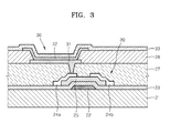
- FIG. 3 is a cross-sectional view of an organic light-emitting device, such as a flat panel display device including a thin film transistor configured as mentioned before.
- the structure illustrated in FIG. 3 represents a single subpixel of the organic light-emitting device.
- Each of such subpixels is a self-emissive device, which includes at least one thin film transistor.
- a separate capacitor is included in each of the subpixels.
- Such an organic light-emitting device may display various pixel patterns according to the emission color of the OLED, preferably including red, green, and blue pixels.
- Such a red (R), green (G), or blue (B) subpixel may include at least more than one TFT, as illustrated in FIG. 3 .
- the organic light-emitting device includes a thin film transistor 20 formed on a substrate 21.
- the substrate 21 may be an insulating substrate. Further, although not shown, a buffer layer may be formed on the substrate 21.
- the thin film transistor 20 includes a gate electrode 22 formed on the substrate 21 in a predetermined pattern, and an insulating layer 23 formed on the gate electrode 22. Then, source and drain electrodes 24a and 24b are each formed on the insulating layer 23 corresponding to the gate electrode 22. The source and drain electrodes 24a and 24b are disposed on a channel layer 25.
- the source and drain electrodes 24a and 24b may be in alternative formed on the insulating layer 23 and the channel layer 25 may be disposed on the source and drain electrodes 24a and 24b as described above.
- a passivation film 27 having a single or multi-layer structure is formed so as to cover the thin film transistor 20.
- the passivation film 27 may include an organic material, an inorganic material, or an organic/inorganic complex material.
- An organic light-emitting film 32 of an EL device 30 is formed on the passivation film 27 in accordance with a pixel-defining film 28.
- the EL device 30, a device displaying predetermined image information by emitting red, green, or blue colored light according to current flow, includes a pixel electrode 31 connected to one of the source and drain electrodes 24a and 24b of the thin film transistor 20, a counter electrode 33 disposed to cover the entire pixel, and an organic light-emitting film 32 disposed between the pixel electrode 31 and the counter electrode 33.
- the pixel electrode 31 and the counter electrode 33 are insulated from each other by the organic light-emitting film 32, and voltage of different polarities is applied to the pixel electrode 31 and the counter electrode 33 to induce light emission from the organic light-emitting film 32.
- the organic light-emitting film 32 may be a low molecular weight or a high molecular weight organic film.
- a hole injection layer (HIL), a hole transport layer (HTL), an emission layer (EML), an electron transport layer (ETL), and an electron injection layer (EIL) may be stacked in a singular or a complex structure to form the organic light-emitting film 32, and the organic material may also include various materials, such as copper phthalocyanine (CuPc), N,N'-di(naphthalene-1-yl)-N,N'-diphenyl-benzidine (NPB), and tris-8-hydroxyquinoline aluminum (Alq3).
- CuPc copper phthalocyanine
- NPB N,N'-di(naphthalene-1-yl)-N,N'-diphenyl-benzidine
- Alq3 tris-8-hydroxyquinoline aluminum
- the high molecular organic film may have a structure including the HTL and the EML, wherein PEDOT may be used to form the HTL, and poly-phenylenevinylene (PPV)-based or polyfluorene-based polymer organic materials may be used to form the EML.
- PEDOT poly-phenylenevinylene
- PPV poly-phenylenevinylene
- Such a high molecular organic film may be formed using screen printing or inkjet printing.
- the pixel electrode 31 may be an anode, and the counter electrode 33 may be a cathode.
- a bottom-oriented film (not shown) covering the pixel electrode 31 may be formed on the liquid crystal display device, thereby completing the manufacture of the bottom substrate of the liquid crystal display device.
- Such a thin film transistor may be mounted on each subpixel as in FIG. 3 , or may be mounted on a driver circuit (not shown) which does not create images.
- FIG. 4 is a spectrum illustrating an XRD analysis result of a channel layer formed in a thin film transistor according to the present invention. Referring to FIG. 4 , it can be verified that the channel layers of the thin film transistors are amorphous, similar to a glass substrate. Thin film 1 represents the channel layer 15 of FIG. 1 , and thin film 2 represents the channel layer 15 of FIG. 2 .
- Two identical glass substrates were sputtered using 12CaO ⁇ 7Al 2 O 3 as a sputter target, at 25% partial oxygen pressure (Ar: 40sccm, O 2 : 13sccm) under a process pressure of 6.0 ⁇ 10 -3 torr with 700 W power RF mode at room temperature.
- the resulting material was heated at 350°C in order to obtain thin films of 29 nm (thin film 1) and 50 nm (thin film 2).
- the thin films were analyzed using XRD and the results are shown in FIG. 4 , along with the XRD spectrum of the glass substrate. Meanwhile, XRD analysis results of the 12CaO ⁇ 7Al 2 O 3 powder used as the thin film-forming sputter target are shown in FIG. 5 . While the 12CaO ⁇ 7Al 2 O 3 powder used as the sputter target in FIG. 5 exhibits crystallinity, the entire thin film formed on the glass substrate was verified to be amorphous as shown in FIG. 4 .
- the index of diffraction (n) and extinction coefficient (k) with regards to thin film 1 were measured at different wavelengths, and are shown in FIG. 6 .
- the obtained amorphous film was verified to have the maximum extinction coefficient at a wavelength of 360.42 nm. This was entered in a relational expression below to obtain a band gap value of the amorphous film of 3.45 eV.
- a glass substrate on which silicon oxide (SiO x ) was formed was prepared, and a gate electrode composed of MoW was formed thereon at a thickness of 200 nm. Then, silicon nitride (SiN x ) was deposited on the gate electrode at a thickness of 200 nm to form an insulating layer.
- the insulating layer was sputtered with 12CaO ⁇ 7Al 2 O 3 as the sputter target, at 25% partial oxygen pressure (Ar: 40sccm, O 2 : 13sccm) and under a process pressure of 6.0 ⁇ 10 -3 torr with a 700 W power at room temperature.
- IZO was deposited on the resulting film to form source and drain electrodes having a thickness of 150 nm, and the structure was heat-treated at a temperature of 350°C to complete the manufacture of a thin film transistor including a channel layer having a thickness of 20 nm.
- a polycrystalline 12CaO ⁇ 7Al 2 O 3 thin film was deposited on an MgO substrate using a PLD method, and was heat-treated at a temperature of 1000°C.
- the resulting thin film was treated with H 2 + at a temperature of 600°C to form a channel layer having a thickness of 1000 nm, and source and drain electrodes formed of Pt were formed thereon at a thickness of 40 nm.
- Y 2 O 3 was deposited on the source and drain electrodes at a thickness of 350 nm to form an insulating layer.
- Au was deposited on the insulating layer at a thickness of 300 ⁇ m to form a gate electrode, thereby completing the manufacture of a thin film transistor.
- the voltage-current characteristics of the thin film transistor of the Comparative Example 1 were evaluated using the same method as in Example 1.
- the field effect mobility remained at 0.05 cm 2 /Vs, and the on-off ratio was 10.
Landscapes
- Physics & Mathematics (AREA)
- Nonlinear Science (AREA)
- Mathematical Physics (AREA)
- Engineering & Computer Science (AREA)
- Chemical & Material Sciences (AREA)
- Crystallography & Structural Chemistry (AREA)
- Microelectronics & Electronic Packaging (AREA)
- General Physics & Mathematics (AREA)
- Optics & Photonics (AREA)
- Thin Film Transistor (AREA)
- Liquid Crystal (AREA)
- Devices For Indicating Variable Information By Combining Individual Elements (AREA)
- Electroluminescent Light Sources (AREA)
Abstract
Description
- The present invention relates to a thin film transistor, a manufacturing method thereof and a flat panel display device including the transistor.
- A field effect transistor is an active device including a gate electrode, source electrode, and a drain electrode, and is operated by applying a voltage to the gate electrode to control a current flowing between the source and drain electrodes. In particular, a field effect transistor using a thin film as a channel layer on an insulating substrate formed of ceramic, glass, or plastic is referred to as a thin film transistor (TFT).
- Because TFTs use a thin film technology, they can be easily formed on a substrate with a relatively large surface area, and are widely used as driving units of flat panel display devices, such as liquid crystal displays (LCDs). That is, image pixels can be turned on or off using TFTs formed on the substrate. In particular, it is predicted that pixel currents can be efficiently controlled by TFTs in future high-performance organic light-emitting devices. Moreover, a TFT circuit driving and controlling the entire image can be formed on the substrate around the image display region, thereby providing a high performance LCD device.
- The most widely used form of TFT uses a polycrystalline silicon film or an amorphous silicon film as a channel layer material. Such a TFT is disclosed in Korean Patent Laid-open Publication No.
1997-0013427 - Organic semiconductor films, such as pentacene, are being developed as a material that can form a film on a plastic substrate at a low temperature. Such organic semiconductors have an aromatic ring, and a large carrier mobility is obtained from the stacking direction of the aromatic ring when crystallized. However, organic semiconductors, such as pentacene, are generally not stable in higher temperatures. An ohmic contact between the source and drain electrode-forming material and the organic semiconducting layer-forming material of a conventional thin film transistor is almost impossible, due to the work function difference between them. Moreover, source and drain electrodes are conventionally composed of inorganic materials, while an organic semiconducting layer is composed of organic materials, and thus the adhesive force between the source/drain electrodes and the organic semiconducting layer is not satisfactory.
- According to a first aspect of the invention, there is provided a top gate or bottom gate thin film transistor, comprising a gate electrode; an insulating layer directly formed on the gate electrode; a channel layer directly formed on the insulating layer; and source and drain electrodes directly formed on and electrically connected to the channel layer. The thin film transistor is characterized in that the channel layer comprises or consists of amorphous 12CaO·7Al2O3.
- Preferably, a thickness of the channel layer (15) is 5 to 200 nm. The thin film transistor may further preferably comprise a substrate made of plastic.
- According to another aspect of the invention, there is provided a flat panel display device comprising the above mentioned thin film transistor. Preferably, the display device is an organic light-emitting device (OLED).
- According to another aspect of the invention, there is provided a method of manufacturing a top gate thin film transistor comprising a gate electrode formed on a substrate; an insulating layer directly formed on the gate electrode; a channel layer directly formed on the insulating layer; and source and drain electrodes directly formed on and electrically connected to the channel layer, wherein the channel layer is formed of 12CaO·7Al2O3. The method includes the steps of:
- forming the gate electrode on the substrate;
- forming the insulating layer directly on the gate electrode;
- depositing a 12CaO·7Al2O3 film directly on the insulating layer by a sputtering process and use of 12CaO·7Al2O3 as a sputter target;
- forming the source and drain electrodes directly on the 12CaO·7Al2O3 film; and
- heat-treating of the resulting product at a temperature of 100 to 600°C.
- According to another aspect of the invention, there is provided a method of manufacturing a bottom gate thin film transistor comprising a gate electrode; an insulating layer directly formed on the gate electrode; a channel layer directly formed on the insulating layer; and source and drain electrodes directly formed on and electrically connected to the channel layer and formed on a substrate, wherein the channel layer is formed of 12CaO·7Al2O3. The method includes the steps of:
- forming source and drain electrodes on the substrate;
- depositing a 12CaO·7Al2O3 film at least between the source and drain electrodes by a sputtering process and use of 12CaO·7Al2O3 as a sputter target;
- forming the insulating layer directly on the 12CaO·7Al2O3 film respectively source and drain electrodes;
- forming the gate electrode directly on the insulating film; and
- heat-treating of the resulting product at a temperature of 100 to 600°C.
- Additional aspects and/or advantages of the invention will be set forth in part in the description which follows and, in part, will be obvious from the description, or may be learned by practice of the invention.
- These and/or other aspects and advantages of the invention will become apparent and more readily appreciated from the following description of the exemplary embodiments, taken in conjunction with the accompanying drawings of which:
-
FIG. 1 is a cross-sectional view schematically illustrating a bottom gate thin film transistor according to an exemplary embodiment of the present invention; -
FIG. 2 is a cross-sectional view schematically illustrating a top gate thin film transistor according to another exemplary embodiment of the present invention; -
FIG. 3 is a cross-sectional view of a flat panel display device including a thin film transistor of the present invention; -
FIG. 4 is a spectrum illustrating an XRD analysis result of the inventive channel layer formed in a thin film transistor; -
FIG. 5 is a spectrum illustrating an XRD analysis result of 12CaO·7Al2O3 powder used as a channel layer-forming sputter target; -
FIG. 6 is a graph illustrating a diffraction rate and absorption coefficient of the inventive channel layer formed in a thin film transistor, measured according to the wavelength; and -
FIG. 7 is a graph illustrating a current-voltage characteristic of a thin film transistor according to an exemplary embodiment of the present invention. - Reference will now be made in detail to the exemplary embodiments of the present invention, examples of which are illustrated in the accompanying drawings, wherein like reference numerals refer to the like elements throughout. The exemplary embodiments are described below in order to explain the present invention by referring to the figures. It will be understood that when an element is referred to as being "disposed on" or "formed on" another element, it may be directly disposed or formed on the other element or intervening elements may be present. In contrast, when an element is referred to as being "directly disposed on" or "directly formed on" another element, there are no intervening elements present. Other words used to describe the relationship between elements should be interpreted in a like fashion (e.g., "between" versus "directly between", "adjacent" versus "directly adjacent", etc.).
- A thin film transistor according to aspects of the present invention includes a channel layer of an amorphous film formed with 12CaO·7Al2O3.
FIG. 1 is a cross-sectional view schematically illustrating a structure of a thin film transistor (TFT) according to an exemplary embodiment of the present invention - Referring to
FIG. 1 , the bottom gate thin film transistor (TFT) according to the current exemplary embodiment of the present invention includes asubstrate 11, a buffer layer 11', agate electrode 12, an insulatinglayer 13, source anddrain electrodes channel layer 15. Thesubstrate 11 may be a metal oxide, such as BaTiO3, LaAlO3, and MgO; an SUS substrate; a glass substrate or a plastic substrate. The buffer layer 11' is formed on thesubstrate 11 and may be formed of SiOx. However, the buffer layer 11' may be omitted. Thegate electrode 12 is formed on the buffer layer 11' and may include or consist of at least one metal or an alloy of two or more selected from the group consisting of Au, Ag, Cu, Ni, Pt, Pd, Al, Mo, Nd, W, ITO and IZO. The insulatinglayer 13 is formed to cover thegate electrode 12. The source anddrain electrodes layer 13. The source anddrain electrodes FIG. 1 , be partially overlapped with thegate electrode 12. The source anddrain electrodes channel layer 15 electrically connecting the source anddrain electrodes drain electrodes FIG. 1 shows thechannel layer 15 formed underneath the source anddrain electrodes channel layer 15 may also be formed on top of the source anddrain electrodes - The
channel layer 15 is formed of an amorphous 12CaO·7Al2O3. Thechannel layer 15 may be formed by heat-treating a film of 12CaO·7Al2O3 deposited at room temperature using a method such as sputtering. The heat-treating is performed at a temperature of 100 to 600°C, preferably 100 to 400°C, and more preferably 300 to 400°C. Since further processes after the heat treatment process are not required in the channel layer forming process, the thin film transistor according to the current exemplary embodiment of the present invention may be manufactured more conveniently than a conventional thin film transistor. - Such a channel layer including the amorphous 12CaO·7Al2O3 is formed at a relatively low temperature, and therefore, substrates formed of metal oxides, such as BaTiO3, LaAlO3, or MgO, as well as a SUS substrate, a glass substrate, or a plastic substrate may be used in the thin film transistor.
- Moreover, since the
channel layer 15 can be formed at a low temperature, thechannel layer 15 can be formed to have a thickness of 200 nm or less, preferably 5 to 200 nm, and more preferably 5 to 100 nm. If the thickness of the channel layer is less than 5 nm, the thin film may not be formed uniformly, and if the thickness of the channel layer is greater than 200 nm, the manufacturing process may become difficult and electrical properties, such as conductivity, may be decreased. - While the band gap value of crystalline 12CaO·7Al2O3 is 6.4 to 6.7 eV, the
amorphous channel layer 15 formed in the thin film transistor has a band gap value in the range of 3 to 4 eV, especially 3 to 3.5 eV. The thin film transistor including a channel layer having such a low band gap range exhibits excellent electrical characteristics. Meanwhile, if the band gap value is less than 3 eV, the thin film transistor cannot be used in visible light display devices due to visible light absorption, which is not desirable. -
FIG. 2 is a cross-sectional view of a top gate thin film transistor according to another exemplary embodiment of the present invention. Referring toFIG. 2 , the thin film transistor includes asubstrate 11, source anddrain electrodes channel layer 15, an insulatinglayer 13, and agate electrode 12. Thesubstrate 11 may be formed of metal, glass, or plastic, or the like as described above. The source anddrain electrodes substrate 11, and are electrically connected to thechannel layer 15. The material forming thechannel layer 15 is as previously described. The insulatinglayer 13 is formed on thechannel layer 15 to insulate thechannel layer 15 from thegate electrode 12. - Although
FIG. 2 illustrates thechannel layer 15 formed on the source anddrain electrodes channel layer 15 being formed on thesubstrate 11 and the source anddrain electrodes layer 13 is disposed between the source and drainelectrode gate electrode 12. Further, the thin film transistor ofFIG. 2 may also include a buffer layer 11' disposed on thesubstrate 11. - A method of manufacturing the thin film transistor according to aspects of the present invention may include, taking the thin film transistor of
FIG. 1 as an example, forming an insulating layer to cover a gate electrode formed on a substrate to insulate the gate electrode; depositing a channel layer-forming 12CaO·7Al2O3 film on the insulating layer; forming source and drain electrodes on the 12CaO·7Al2O3 film; and heat-treating the resulting product at 100 to 600°C to form the channel layer. - If necessary, the source and
drain electrodes layer 13, and then the channel layer-forming 12CaO·7Al2O3 film may be deposited so as to cover the source anddrain electrodes - The thin film transistor having the above-described structure may be included in a flat panel display device such as an LCD or an organic light-emitting device (OLED).
FIG. 3 is a cross-sectional view of an organic light-emitting device, such as a flat panel display device including a thin film transistor configured as mentioned before. The structure illustrated inFIG. 3 represents a single subpixel of the organic light-emitting device. Each of such subpixels is a self-emissive device, which includes at least one thin film transistor. Moreover, although not illustrated inFIG. 3 , a separate capacitor is included in each of the subpixels. Such an organic light-emitting device may display various pixel patterns according to the emission color of the OLED, preferably including red, green, and blue pixels. - Such a red (R), green (G), or blue (B) subpixel may include at least more than one TFT, as illustrated in
FIG. 3 . - Referring to
FIG. 3 , the organic light-emitting device includes athin film transistor 20 formed on asubstrate 21. Thesubstrate 21 may be an insulating substrate. Further, although not shown, a buffer layer may be formed on thesubstrate 21. Thethin film transistor 20 includes agate electrode 22 formed on thesubstrate 21 in a predetermined pattern, and an insulatinglayer 23 formed on thegate electrode 22. Then, source anddrain electrodes layer 23 corresponding to thegate electrode 22. The source anddrain electrodes channel layer 25. However, the source anddrain electrodes layer 23 and thechannel layer 25 may be disposed on the source anddrain electrodes channel layer 25 is formed, apassivation film 27 having a single or multi-layer structure is formed so as to cover thethin film transistor 20. Thepassivation film 27 may include an organic material, an inorganic material, or an organic/inorganic complex material. An organic light-emittingfilm 32 of anEL device 30 is formed on thepassivation film 27 in accordance with a pixel-definingfilm 28. TheEL device 30, a device displaying predetermined image information by emitting red, green, or blue colored light according to current flow, includes apixel electrode 31 connected to one of the source anddrain electrodes thin film transistor 20, acounter electrode 33 disposed to cover the entire pixel, and an organic light-emittingfilm 32 disposed between thepixel electrode 31 and thecounter electrode 33. - The
pixel electrode 31 and thecounter electrode 33 are insulated from each other by the organic light-emittingfilm 32, and voltage of different polarities is applied to thepixel electrode 31 and thecounter electrode 33 to induce light emission from the organic light-emittingfilm 32. The organic light-emittingfilm 32 may be a low molecular weight or a high molecular weight organic film. If the organic light-emittingfilm 32 is formed of a low molecular organic film , a hole injection layer (HIL), a hole transport layer (HTL), an emission layer (EML), an electron transport layer (ETL), and an electron injection layer (EIL) may be stacked in a singular or a complex structure to form the organic light-emittingfilm 32, and the organic material may also include various materials, such as copper phthalocyanine (CuPc), N,N'-di(naphthalene-1-yl)-N,N'-diphenyl-benzidine (NPB), and tris-8-hydroxyquinoline aluminum (Alq3). Such a low molecular organic film may be formed using vacuum deposition. The high molecular organic film may have a structure including the HTL and the EML, wherein PEDOT may be used to form the HTL, and poly-phenylenevinylene (PPV)-based or polyfluorene-based polymer organic materials may be used to form the EML. Such a high molecular organic film may be formed using screen printing or inkjet printing. - The
pixel electrode 31 may be an anode, and thecounter electrode 33 may be a cathode. In the case of a liquid crystal display device, contrastingly, a bottom-oriented film (not shown) covering thepixel electrode 31 may be formed on the liquid crystal display device, thereby completing the manufacture of the bottom substrate of the liquid crystal display device. Such a thin film transistor may be mounted on each subpixel as inFIG. 3 , or may be mounted on a driver circuit (not shown) which does not create images. -
FIG. 4 is a spectrum illustrating an XRD analysis result of a channel layer formed in a thin film transistor according to the present invention. Referring toFIG. 4 , it can be verified that the channel layers of the thin film transistors are amorphous, similar to a glass substrate.Thin film 1 represents thechannel layer 15 ofFIG. 1 , andthin film 2 represents thechannel layer 15 ofFIG. 2 . - Aspects of the present invention will now be described with reference to the following examples.
- Examples
- <Assessment of 12CaO·7Al2O3 Thin Film Properties>
- Two identical glass substrates were sputtered using 12CaO·7Al2O3 as a sputter target, at 25% partial oxygen pressure (Ar: 40sccm, O2: 13sccm) under a process pressure of 6.0 ×10⁻³ torr with 700 W power RF mode at room temperature. The resulting material was heated at 350°C in order to obtain thin films of 29 nm (thin film 1) and 50 nm (thin film 2).
- The thin films were analyzed using XRD and the results are shown in
FIG. 4 , along with the XRD spectrum of the glass substrate. Meanwhile, XRD analysis results of the 12CaO·7Al2O3 powder used as the thin film-forming sputter target are shown inFIG. 5 . While the 12CaO·7Al2O3 powder used as the sputter target inFIG. 5 exhibits crystallinity, the entire thin film formed on the glass substrate was verified to be amorphous as shown inFIG. 4 . - Furthermore, the index of diffraction (n) and extinction coefficient (k) with regards to
thin film 1 were measured at different wavelengths, and are shown inFIG. 6 . Referring toFIG. 6 , the obtained amorphous film was verified to have the maximum extinction coefficient at a wavelength of 360.42 nm. This was entered in a relational expression below to obtain a band gap value of the amorphous film of 3.45 eV. - E = hc/λ (h=4.14×10⁻¹⁵ eV, c=3×10⁸ m/s)
- <Manufacturing of Thin Film Transistor>
- Example 1
- A glass substrate on which silicon oxide (SiOx) was formed was prepared, and a gate electrode composed of MoW was formed thereon at a thickness of 200 nm. Then, silicon nitride (SiNx) was deposited on the gate electrode at a thickness of 200 nm to form an insulating layer. The insulating layer was sputtered with 12CaO·7Al2O3 as the sputter target, at 25% partial oxygen pressure (Ar: 40sccm, O2: 13sccm) and under a process pressure of 6.0 ×10⁻³ torr with a 700 W power at room temperature. Then, IZO was deposited on the resulting film to form source and drain electrodes having a thickness of 150 nm, and the structure was heat-treated at a temperature of 350°C to complete the manufacture of a thin film transistor including a channel layer having a thickness of 20 nm.
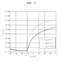
- Evaluation of voltage-current characteristics was performed using an HP4155 (a probe station of HP Inc). The voltage-current characteristics of the obtained thin film transistor were evaluated, and a linear mobility measured at VDS=0.1V and saturation mobilities measured at VDS=5.1V and VDS=10.1V were obtained. Referring to
FIG. 7 , the linear mobility was 9.54cm2/Vs, the saturation mobility was 1.68cm2/Vs, threshold voltage was 9.8V, and on-off ratio was 9.67×10⁶, demonstrating that the organic thin film transistor has excellent electrical characteristics. - Comparative Example 1
- A polycrystalline 12CaO·7Al2O3 thin film was deposited on an MgO substrate using a PLD method, and was heat-treated at a temperature of 1000°C. The resulting thin film was treated with H2 + at a temperature of 600°C to form a channel layer having a thickness of 1000 nm, and source and drain electrodes formed of Pt were formed thereon at a thickness of 40 nm. Y2O3 was deposited on the source and drain electrodes at a thickness of 350 nm to form an insulating layer. Then, Au was deposited on the insulating layer at a thickness of 300 µm to form a gate electrode, thereby completing the manufacture of a thin film transistor.
- The voltage-current characteristics of the thin film transistor of the Comparative Example 1 were evaluated using the same method as in Example 1. The field effect mobility remained at 0.05 cm2/Vs, and the on-off ratio was 10.
Claims (7)
- A top gate or bottom gate thin film transistor, comprising:a gate electrode (12);an insulating layer (13) directly formed on the gate electrode (12);a channel layer (15) directly formed on the insulating layer (13); andsource and drain electrodes (14a, 14b) directly formed on and electrically connected to the channel layer (15),characterized in thatthe channel layer (15) comprises or consists of amorphous 12CaO·7Al2O3.
- The thin film transistor of claim 1, wherein a thickness of the channel layer (15) is 5 to 200 nm.
- The thin film transistor of claim 1 or 2, wherein the thin film transistor comprises a substrate (11) made of plastic.
- A flat panel display device comprising:a thin film transistor according to any of claims 1 through 3.
- The flat panel display device of claim 4, wherein the display device is an organic light-emitting device (OLED).
- Method of manufacturing a top gate thin film transistor comprising:a gate electrode (12) formed on a substrate (11);an insulating layer (13) directly formed on the gate electrode (12);a channel layer (15) directly formed on the insulating layer (13), wherein the channel layer is formed of 12CaO·7Al2O3;source and drain electrodes (14a, 14b) directly formed on and electrically connected to the channel layer (15);the method including the steps of:- forming the gate electrode (12) on the substrate (11);- forming the insulating layer (13) directly on the gate electrode (12);- depositing a 12CaO·7Al2O3 film directly on the insulating layer (13) by a sputtering process and use of 12CaO·7Al2O3 as a sputter target;- forming the source and drain electrodes (14a, 14b) directly on the 12CaO·7Al2O3 film; and- heat-treating of the resulting product at a temperature of 100 to 600°C.
- Method of manufacturing a bottom gate thin film transistor comprising:a gate electrode (12);an insulating layer (13) directly formed on the gate electrode (12);a channel layer (15) directly formed on the insulating layer (13), wherein the channel layer is formed of 12CaO·7Al2O3;source and drain electrodes (14a, 14b) directly formed on and electrically connected to the channel layer (15) and formed on a substrate (11);the method including the steps of:- forming source and drain electrodes (14a, 14b) on the substrate (11);- depositing a 12CaO·7Al2O3 film at least between the source and drain electrodes (14a, 14b) by a sputtering process and use of 12CaO·7Al2O3 as a sputter target;- forming the insulating layer (13) directly on the 12CaO·7Al2O3 film respectively source and drain electrodes (14a, 14b);- forming the gate electrode (12) directly on the insulating film (13); and- heat-treating of the resulting product at a temperature of 100 to 600°C.
Applications Claiming Priority (1)
| Application Number | Priority Date | Filing Date | Title |
|---|---|---|---|
| KR1020080019692A KR100918404B1 (en) | 2008-03-03 | 2008-03-03 | Thin film transistor and flat panel display device using same |
Publications (2)
| Publication Number | Publication Date |
|---|---|
| EP2099074A1 true EP2099074A1 (en) | 2009-09-09 |
| EP2099074B1 EP2099074B1 (en) | 2010-09-29 |
Family
ID=40671167
Family Applications (1)
| Application Number | Title | Priority Date | Filing Date |
|---|---|---|---|
| EP09153911A Ceased EP2099074B1 (en) | 2008-03-03 | 2009-02-27 | Thin film transistor, manufacturing method thereof and flat panel display including the same thin film transistor |
Country Status (6)
| Country | Link |
|---|---|
| US (1) | US8067770B2 (en) |
| EP (1) | EP2099074B1 (en) |
| JP (1) | JP5020276B2 (en) |
| KR (1) | KR100918404B1 (en) |
| CN (1) | CN101527321B (en) |
| DE (1) | DE602009000232D1 (en) |
Families Citing this family (14)
| Publication number | Priority date | Publication date | Assignee | Title |
|---|---|---|---|---|
| JP5106313B2 (en) * | 2008-08-13 | 2012-12-26 | 独立行政法人科学技術振興機構 | Method for forming ohmic junction to the surface of conductive element material comprising C12A7 electride |
| JP5760298B2 (en) * | 2009-05-21 | 2015-08-05 | ソニー株式会社 | Thin film transistor, display device, and electronic device |
| CN102473732B (en) * | 2009-07-27 | 2015-09-16 | 株式会社神户制钢所 | Wiring structure and display device with wiring structure |
| US8884282B2 (en) * | 2010-04-02 | 2014-11-11 | Semiconductor Energy Laboratory Co., Ltd. | Semiconductor device |
| US8921948B2 (en) * | 2011-01-12 | 2014-12-30 | Semiconductor Energy Laboratory Co., Ltd. | Semiconductor device and manufacturing method thereof |
| TWI589043B (en) * | 2012-06-20 | 2017-06-21 | Japan Science & Tech Agency | Organic electroluminescent device |
| JP6198276B2 (en) * | 2012-06-20 | 2017-09-20 | 国立研究開発法人科学技術振興機構 | C12A7 electride thin film manufacturing method and C12A7 electride thin film |
| CN102955312B (en) * | 2012-11-14 | 2015-05-20 | 京东方科技集团股份有限公司 | Array substrate and manufacture method thereof and display device |
| KR102029072B1 (en) * | 2012-12-28 | 2019-10-07 | 엘지디스플레이 주식회사 | Flexible Display Device and Method for fabricating the same |
| KR102048892B1 (en) | 2013-05-15 | 2019-11-27 | 삼성디스플레이 주식회사 | Inorganic oxide thin layer and method for preparing the same |
| JP6149725B2 (en) * | 2013-05-28 | 2017-06-21 | 旭硝子株式会社 | Semiconductor device and manufacturing method of semiconductor device |
| DE102015103651B4 (en) * | 2015-03-12 | 2017-11-16 | Osram Oled Gmbh | Process for the production of electrically conductive structures and organic light emitting diode |
| KR102442616B1 (en) | 2015-04-08 | 2022-09-14 | 삼성디스플레이 주식회사 | Organic light emitting display device and manufacturing method thereof |
| CN108963109B (en) * | 2018-06-29 | 2020-10-09 | 云谷(固安)科技有限公司 | An organic electroluminescent device |
Citations (2)
| Publication number | Priority date | Publication date | Assignee | Title |
|---|---|---|---|---|
| KR970013427A (en) | 1995-08-25 | 1997-03-29 | 김광호 | Thin film transistor for liquid crystal display device and manufacturing method thereof |
| US20050199879A1 (en) * | 2004-03-12 | 2005-09-15 | Hoffman Randy L. | Semiconductor device |
Family Cites Families (5)
| Publication number | Priority date | Publication date | Assignee | Title |
|---|---|---|---|---|
| US7662357B2 (en) * | 2002-04-19 | 2010-02-16 | Japan Science And Technology Agency | Hydrogen-containing electrically conductive inorganic compound |
| KR100615235B1 (en) * | 2004-08-05 | 2006-08-25 | 삼성에스디아이 주식회사 | Organic thin film transistor groups and flat panel display device having same |
| JP4850457B2 (en) * | 2005-09-06 | 2012-01-11 | キヤノン株式会社 | Thin film transistor and thin film diode |
| JP5376750B2 (en) * | 2005-11-18 | 2013-12-25 | 出光興産株式会社 | Semiconductor thin film, manufacturing method thereof, thin film transistor, active matrix drive display panel |
| JP2008227316A (en) * | 2007-03-14 | 2008-09-25 | Seiko Epson Corp | SEMICONDUCTOR DEVICE, SEMICONDUCTOR DEVICE MANUFACTURING METHOD, AND ELECTRONIC DEVICE |
-
2008
- 2008-03-03 KR KR1020080019692A patent/KR100918404B1/en active Active
- 2008-07-31 US US12/183,451 patent/US8067770B2/en active Active
-
2009
- 2009-02-19 CN CN2009100056966A patent/CN101527321B/en not_active Expired - Fee Related
- 2009-02-27 DE DE602009000232T patent/DE602009000232D1/en active Active
- 2009-02-27 EP EP09153911A patent/EP2099074B1/en not_active Ceased
- 2009-03-02 JP JP2009048292A patent/JP5020276B2/en not_active Expired - Fee Related
Patent Citations (2)
| Publication number | Priority date | Publication date | Assignee | Title |
|---|---|---|---|---|
| KR970013427A (en) | 1995-08-25 | 1997-03-29 | 김광호 | Thin film transistor for liquid crystal display device and manufacturing method thereof |
| US20050199879A1 (en) * | 2004-03-12 | 2005-09-15 | Hoffman Randy L. | Semiconductor device |
Non-Patent Citations (1)
| Title |
|---|
| HOSONO ET AL: "Recent progress in transparent oxide semiconductors: Materials and device application", THIN SOLID FILMS, ELSEVIER-SEQUOIA S.A. LAUSANNE, CH, vol. 515, no. 15, 27 April 2007 (2007-04-27), pages 6000 - 6014, XP022212810, ISSN: 0040-6090 * |
Also Published As
| Publication number | Publication date |
|---|---|
| DE602009000232D1 (en) | 2010-11-11 |
| US8067770B2 (en) | 2011-11-29 |
| KR100918404B1 (en) | 2009-09-24 |
| CN101527321B (en) | 2013-03-20 |
| KR20090094626A (en) | 2009-09-08 |
| CN101527321A (en) | 2009-09-09 |
| JP2009212520A (en) | 2009-09-17 |
| JP5020276B2 (en) | 2012-09-05 |
| EP2099074B1 (en) | 2010-09-29 |
| US20090218570A1 (en) | 2009-09-03 |
Similar Documents
| Publication | Publication Date | Title |
|---|---|---|
| EP2099074B1 (en) | Thin film transistor, manufacturing method thereof and flat panel display including the same thin film transistor | |
| KR100858821B1 (en) | A thin film transistor, a method of manufacturing the same, and an organic light emitting display device including the thin film transistor and a method of manufacturing the same | |
| US8729552B2 (en) | Backplane for flat panel display apparatus, flat panel display apparatus including the same, and method of manufacturing backplane for flat panel display apparatus | |
| US10388716B2 (en) | Organic light-emitting display apparatus | |
| US20100006837A1 (en) | Composition for oxide semiconductor thin film, field effect transistor using the composition and method of fabricating the transistor | |
| KR20110057985A (en) | Flexible display device and manufacturing method thereof | |
| US7470931B2 (en) | Thin film transistor and flat panel display using the same | |
| KR100990217B1 (en) | Composition for oxide semiconductor thin film, field effect transistor using same and method for manufacturing same | |
| US20130001566A1 (en) | Back plane for use in flat panel displays and method of manufacturing the back plane | |
| US20140312315A1 (en) | Back plane of flat panel display and method of manufacturing the same | |
| KR20070005399A (en) | Flat panel display device and manufacturing method thereof | |
| US20150028300A1 (en) | Thin film transistor, organic light-emitting display apparatus including the same, and method of manufacturing the thin film transistor | |
| KR100592302B1 (en) | A method of manufacturing a substrate having a thin film transistor, a substrate having a thin film transistor manufactured thereby, a method of manufacturing a flat panel display device, and a flat panel display device manufactured accordingly | |
| US20060255336A1 (en) | Thin film transistor and method of manufacturing the same | |
| US8227326B2 (en) | Laser crystallization of amorphous silicon layer | |
| JP5553868B2 (en) | Display device using oxide semiconductor and manufacturing method thereof | |
| KR100603329B1 (en) | Thin film transistor and flat panel display device having same | |
| KR100669702B1 (en) | Thin film transistor and flat panel display device having same | |
| KR101193176B1 (en) | A method for preparing flat display device and the flat display device prepared by the method | |
| KR100647629B1 (en) | A method of manufacturing a substrate having a thin film transistor, a substrate having a thin film transistor manufactured thereby, a method of manufacturing a flat panel display device, and a flat panel display device manufactured accordingly | |
| KR100696507B1 (en) | A method of manufacturing a thin film transistor employing a polycrystalline silicon film, a thin film transistor manufactured according to this, and a flat panel display device having the thin film transistor | |
| KR100759555B1 (en) | Flat panel display apparatus and method of manufacturing the same apparatus | |
| KR20190015985A (en) | Method of manufacturing semiconductor device |
Legal Events
| Date | Code | Title | Description |
|---|---|---|---|
| PUAI | Public reference made under article 153(3) epc to a published international application that has entered the european phase |
Free format text: ORIGINAL CODE: 0009012 |
|
| 17P | Request for examination filed |
Effective date: 20090227 |
|
| AK | Designated contracting states |
Kind code of ref document: A1 Designated state(s): AT BE BG CH CY CZ DE DK EE ES FI FR GB GR HR HU IE IS IT LI LT LU LV MC MK MT NL NO PL PT RO SE SI SK TR |
|
| AX | Request for extension of the european patent |
Extension state: AL BA RS |
|
| GRAP | Despatch of communication of intention to grant a patent |
Free format text: ORIGINAL CODE: EPIDOSNIGR1 |
|
| GRAS | Grant fee paid |
Free format text: ORIGINAL CODE: EPIDOSNIGR3 |
|
| AKX | Designation fees paid |
Designated state(s): DE FR GB |
|
| RIN1 | Information on inventor provided before grant (corrected) |
Inventor name: SONG, YOUNG-WOO Inventor name: LEE, JONG-HYUK Inventor name: KIM, YONG-TAK Inventor name: HA, JAE-HEUNG |
|
| GRAA | (expected) grant |
Free format text: ORIGINAL CODE: 0009210 |
|
| RIN1 | Information on inventor provided before grant (corrected) |
Inventor name: LEE, JONG-HYUK Inventor name: KIM, YONG-TAK Inventor name: SONG, YOUNG-WOO Inventor name: HA, JAE-HEUNG |
|
| AK | Designated contracting states |
Kind code of ref document: B1 Designated state(s): DE FR GB |
|
| REG | Reference to a national code |
Ref country code: GB Ref legal event code: FG4D |
|
| REF | Corresponds to: |
Ref document number: 602009000232 Country of ref document: DE Date of ref document: 20101111 Kind code of ref document: P |
|
| PLBE | No opposition filed within time limit |
Free format text: ORIGINAL CODE: 0009261 |
|
| STAA | Information on the status of an ep patent application or granted ep patent |
Free format text: STATUS: NO OPPOSITION FILED WITHIN TIME LIMIT |
|
| REG | Reference to a national code |
Ref country code: DE Ref legal event code: R097 Ref document number: 602009000232 Country of ref document: DE Effective date: 20110630 |
|
| REG | Reference to a national code |
Ref country code: DE Ref legal event code: R082 Ref document number: 602009000232 Country of ref document: DE Representative=s name: GULDE HENGELHAUPT ZIEBIG & SCHNEIDER, DE |
|
| REG | Reference to a national code |
Ref country code: DE Ref legal event code: R081 Ref document number: 602009000232 Country of ref document: DE Owner name: SAMSUNG DISPLAY CO., LTD., KR Free format text: FORMER OWNER: SAMSUNG MOBILE DISPLAY CO. LTD., SUWON, KR Effective date: 20120921 Ref country code: DE Ref legal event code: R082 Ref document number: 602009000232 Country of ref document: DE Representative=s name: GULDE HENGELHAUPT ZIEBIG & SCHNEIDER, DE Effective date: 20120921 Ref country code: DE Ref legal event code: R081 Ref document number: 602009000232 Country of ref document: DE Owner name: SAMSUNG DISPLAY CO., LTD., YONGIN-CITY, KR Free format text: FORMER OWNER: SAMSUNG MOBILE DISPLAY CO. LTD., SUWON, GYEONGGI, KR Effective date: 20120921 Ref country code: DE Ref legal event code: R082 Ref document number: 602009000232 Country of ref document: DE Representative=s name: GULDE & PARTNER PATENT- UND RECHTSANWALTSKANZL, DE Effective date: 20120921 |
|
| REG | Reference to a national code |
Ref country code: GB Ref legal event code: 732E Free format text: REGISTERED BETWEEN 20130110 AND 20130116 |
|
| REG | Reference to a national code |
Ref country code: FR Ref legal event code: TP Owner name: SAMSUNG MOBILE DISPLAY CO., LTD., KR Effective date: 20130220 |
|
| REG | Reference to a national code |
Ref country code: FR Ref legal event code: PLFP Year of fee payment: 8 |
|
| REG | Reference to a national code |
Ref country code: FR Ref legal event code: PLFP Year of fee payment: 9 |
|
| REG | Reference to a national code |
Ref country code: FR Ref legal event code: PLFP Year of fee payment: 10 |
|
| P01 | Opt-out of the competence of the unified patent court (upc) registered |
Effective date: 20230515 |
|
| PGFP | Annual fee paid to national office [announced via postgrant information from national office to epo] |
Ref country code: DE Payment date: 20240122 Year of fee payment: 16 Ref country code: GB Payment date: 20240122 Year of fee payment: 16 |
|
| PGFP | Annual fee paid to national office [announced via postgrant information from national office to epo] |
Ref country code: FR Payment date: 20240123 Year of fee payment: 16 |
|
| REG | Reference to a national code |
Ref country code: DE Ref legal event code: R079 Ref document number: 602009000232 Country of ref document: DE Free format text: PREVIOUS MAIN CLASS: H01L0029786000 Ipc: H10D0030670000 |
|
| REG | Reference to a national code |
Ref country code: DE Ref legal event code: R119 Ref document number: 602009000232 Country of ref document: DE |
|
| GBPC | Gb: european patent ceased through non-payment of renewal fee |
Effective date: 20250227 |
|
| PG25 | Lapsed in a contracting state [announced via postgrant information from national office to epo] |
Ref country code: DE Free format text: LAPSE BECAUSE OF NON-PAYMENT OF DUE FEES Effective date: 20250902 |
|
| PG25 | Lapsed in a contracting state [announced via postgrant information from national office to epo] |
Ref country code: GB Free format text: LAPSE BECAUSE OF NON-PAYMENT OF DUE FEES Effective date: 20250227 |
|
| PG25 | Lapsed in a contracting state [announced via postgrant information from national office to epo] |
Ref country code: FR Free format text: LAPSE BECAUSE OF NON-PAYMENT OF DUE FEES Effective date: 20250228 |