EP2097904B1 - Memory cell, and method for storing data - Google Patents
Memory cell, and method for storing data Download PDFInfo
- Publication number
- EP2097904B1 EP2097904B1 EP07846385A EP07846385A EP2097904B1 EP 2097904 B1 EP2097904 B1 EP 2097904B1 EP 07846385 A EP07846385 A EP 07846385A EP 07846385 A EP07846385 A EP 07846385A EP 2097904 B1 EP2097904 B1 EP 2097904B1
- Authority
- EP
- European Patent Office
- Prior art keywords
- memory cell
- potential well
- semiconductor
- charged state
- semiconductor heterostructure
- Prior art date
- Legal status (The legal status is an assumption and is not a legal conclusion. Google has not performed a legal analysis and makes no representation as to the accuracy of the status listed.)
- Active
Links
- 230000015654 memory Effects 0.000 title claims abstract description 116
- 238000000034 method Methods 0.000 title claims description 19
- 239000004065 semiconductor Substances 0.000 claims abstract description 88
- 239000010410 layer Substances 0.000 claims description 118
- 239000002800 charge carrier Substances 0.000 claims description 47
- 239000000463 material Substances 0.000 claims description 35
- 239000002086 nanomaterial Substances 0.000 claims description 23
- 239000011229 interlayer Substances 0.000 claims description 8
- 230000001419 dependent effect Effects 0.000 claims description 6
- 238000011156 evaluation Methods 0.000 claims description 6
- 230000000694 effects Effects 0.000 claims description 3
- 230000005533 two-dimensional electron gas Effects 0.000 claims description 3
- 230000009467 reduction Effects 0.000 claims description 2
- 210000004027 cell Anatomy 0.000 description 81
- 230000004888 barrier function Effects 0.000 description 16
- 125000006850 spacer group Chemical group 0.000 description 12
- 230000008569 process Effects 0.000 description 9
- 230000014759 maintenance of location Effects 0.000 description 6
- 230000008901 benefit Effects 0.000 description 5
- 238000007667 floating Methods 0.000 description 5
- 229910004298 SiO 2 Inorganic materials 0.000 description 4
- 239000002096 quantum dot Substances 0.000 description 4
- 230000005641 tunneling Effects 0.000 description 4
- 229910000673 Indium arsenide Inorganic materials 0.000 description 3
- 229910052738 indium Inorganic materials 0.000 description 3
- RPQDHPTXJYYUPQ-UHFFFAOYSA-N indium arsenide Chemical compound [In]#[As] RPQDHPTXJYYUPQ-UHFFFAOYSA-N 0.000 description 3
- 239000011159 matrix material Substances 0.000 description 3
- 229910005542 GaSb Inorganic materials 0.000 description 2
- 230000006399 behavior Effects 0.000 description 2
- 230000000903 blocking effect Effects 0.000 description 2
- 238000004891 communication Methods 0.000 description 2
- 239000002784 hot electron Substances 0.000 description 2
- WPYVAWXEWQSOGY-UHFFFAOYSA-N indium antimonide Chemical compound [Sb]#[In] WPYVAWXEWQSOGY-UHFFFAOYSA-N 0.000 description 2
- APFVFJFRJDLVQX-UHFFFAOYSA-N indium atom Chemical compound [In] APFVFJFRJDLVQX-UHFFFAOYSA-N 0.000 description 2
- 238000002347 injection Methods 0.000 description 2
- 239000007924 injection Substances 0.000 description 2
- 238000004377 microelectronic Methods 0.000 description 2
- 210000000352 storage cell Anatomy 0.000 description 2
- 239000000758 substrate Substances 0.000 description 2
- RSIWALKZYXPAGW-NSHDSACASA-N 6-(3-fluorophenyl)-3-methyl-7-[(1s)-1-(7h-purin-6-ylamino)ethyl]-[1,3]thiazolo[3,2-a]pyrimidin-5-one Chemical compound C=1([C@@H](NC=2C=3N=CNC=3N=CN=2)C)N=C2SC=C(C)N2C(=O)C=1C1=CC=CC(F)=C1 RSIWALKZYXPAGW-NSHDSACASA-N 0.000 description 1
- 241000819038 Chichester Species 0.000 description 1
- 229910001218 Gallium arsenide Inorganic materials 0.000 description 1
- 230000015572 biosynthetic process Effects 0.000 description 1
- 239000003990 capacitor Substances 0.000 description 1
- 239000000969 carrier Substances 0.000 description 1
- 230000008859 change Effects 0.000 description 1
- 230000003247 decreasing effect Effects 0.000 description 1
- 238000013461 design Methods 0.000 description 1
- 238000011161 development Methods 0.000 description 1
- 230000018109 developmental process Effects 0.000 description 1
- 238000007599 discharging Methods 0.000 description 1
- 238000005265 energy consumption Methods 0.000 description 1
- 238000005516 engineering process Methods 0.000 description 1
- 230000006870 function Effects 0.000 description 1
- 238000009413 insulation Methods 0.000 description 1
- 230000003993 interaction Effects 0.000 description 1
- 238000005036 potential barrier Methods 0.000 description 1
- 239000002356 single layer Substances 0.000 description 1
- 238000001228 spectrum Methods 0.000 description 1
- 238000012546 transfer Methods 0.000 description 1
- 230000007704 transition Effects 0.000 description 1
Images


Classifications
-
- G—PHYSICS
- G11—INFORMATION STORAGE
- G11C—STATIC STORES
- G11C16/00—Erasable programmable read-only memories
- G11C16/02—Erasable programmable read-only memories electrically programmable
-
- H—ELECTRICITY
- H01—ELECTRIC ELEMENTS
- H01L—SEMICONDUCTOR DEVICES NOT COVERED BY CLASS H10
- H01L29/00—Semiconductor devices adapted for rectifying, amplifying, oscillating or switching, or capacitors or resistors with at least one potential-jump barrier or surface barrier, e.g. PN junction depletion layer or carrier concentration layer; Details of semiconductor bodies or of electrodes thereof ; Multistep manufacturing processes therefor
- H01L29/66—Types of semiconductor device ; Multistep manufacturing processes therefor
- H01L29/86—Types of semiconductor device ; Multistep manufacturing processes therefor controllable only by variation of the electric current supplied, or only the electric potential applied, to one or more of the electrodes carrying the current to be rectified, amplified, oscillated or switched
- H01L29/861—Diodes
- H01L29/8613—Mesa PN junction diodes
-
- B—PERFORMING OPERATIONS; TRANSPORTING
- B82—NANOTECHNOLOGY
- B82Y—SPECIFIC USES OR APPLICATIONS OF NANOSTRUCTURES; MEASUREMENT OR ANALYSIS OF NANOSTRUCTURES; MANUFACTURE OR TREATMENT OF NANOSTRUCTURES
- B82Y10/00—Nanotechnology for information processing, storage or transmission, e.g. quantum computing or single electron logic
-
- H—ELECTRICITY
- H01—ELECTRIC ELEMENTS
- H01L—SEMICONDUCTOR DEVICES NOT COVERED BY CLASS H10
- H01L29/00—Semiconductor devices adapted for rectifying, amplifying, oscillating or switching, or capacitors or resistors with at least one potential-jump barrier or surface barrier, e.g. PN junction depletion layer or carrier concentration layer; Details of semiconductor bodies or of electrodes thereof ; Multistep manufacturing processes therefor
- H01L29/02—Semiconductor bodies ; Multistep manufacturing processes therefor
- H01L29/12—Semiconductor bodies ; Multistep manufacturing processes therefor characterised by the materials of which they are formed
- H01L29/122—Single quantum well structures
- H01L29/127—Quantum box structures
-
- H—ELECTRICITY
- H01—ELECTRIC ELEMENTS
- H01L—SEMICONDUCTOR DEVICES NOT COVERED BY CLASS H10
- H01L29/00—Semiconductor devices adapted for rectifying, amplifying, oscillating or switching, or capacitors or resistors with at least one potential-jump barrier or surface barrier, e.g. PN junction depletion layer or carrier concentration layer; Details of semiconductor bodies or of electrodes thereof ; Multistep manufacturing processes therefor
- H01L29/02—Semiconductor bodies ; Multistep manufacturing processes therefor
- H01L29/12—Semiconductor bodies ; Multistep manufacturing processes therefor characterised by the materials of which they are formed
- H01L29/20—Semiconductor bodies ; Multistep manufacturing processes therefor characterised by the materials of which they are formed including, apart from doping materials or other impurities, only AIIIBV compounds
- H01L29/201—Semiconductor bodies ; Multistep manufacturing processes therefor characterised by the materials of which they are formed including, apart from doping materials or other impurities, only AIIIBV compounds including two or more compounds, e.g. alloys
- H01L29/205—Semiconductor bodies ; Multistep manufacturing processes therefor characterised by the materials of which they are formed including, apart from doping materials or other impurities, only AIIIBV compounds including two or more compounds, e.g. alloys in different semiconductor regions, e.g. heterojunctions
-
- H—ELECTRICITY
- H01—ELECTRIC ELEMENTS
- H01L—SEMICONDUCTOR DEVICES NOT COVERED BY CLASS H10
- H01L29/00—Semiconductor devices adapted for rectifying, amplifying, oscillating or switching, or capacitors or resistors with at least one potential-jump barrier or surface barrier, e.g. PN junction depletion layer or carrier concentration layer; Details of semiconductor bodies or of electrodes thereof ; Multistep manufacturing processes therefor
- H01L29/66—Types of semiconductor device ; Multistep manufacturing processes therefor
- H01L29/68—Types of semiconductor device ; Multistep manufacturing processes therefor controllable by only the electric current supplied, or only the electric potential applied, to an electrode which does not carry the current to be rectified, amplified or switched
- H01L29/76—Unipolar devices, e.g. field effect transistors
- H01L29/772—Field effect transistors
- H01L29/78—Field effect transistors with field effect produced by an insulated gate
- H01L29/788—Field effect transistors with field effect produced by an insulated gate with floating gate
-
- H—ELECTRICITY
- H01—ELECTRIC ELEMENTS
- H01L—SEMICONDUCTOR DEVICES NOT COVERED BY CLASS H10
- H01L29/00—Semiconductor devices adapted for rectifying, amplifying, oscillating or switching, or capacitors or resistors with at least one potential-jump barrier or surface barrier, e.g. PN junction depletion layer or carrier concentration layer; Details of semiconductor bodies or of electrodes thereof ; Multistep manufacturing processes therefor
- H01L29/66—Types of semiconductor device ; Multistep manufacturing processes therefor
- H01L29/86—Types of semiconductor device ; Multistep manufacturing processes therefor controllable only by variation of the electric current supplied, or only the electric potential applied, to one or more of the electrodes carrying the current to be rectified, amplified, oscillated or switched
- H01L29/861—Diodes
- H01L29/8616—Charge trapping diodes
-
- G—PHYSICS
- G11—INFORMATION STORAGE
- G11C—STATIC STORES
- G11C2216/00—Indexing scheme relating to G11C16/00 and subgroups, for features not directly covered by these groups
- G11C2216/02—Structural aspects of erasable programmable read-only memories
- G11C2216/08—Nonvolatile memory wherein data storage is accomplished by storing relatively few electrons in the storage layer, i.e. single electron memory
Definitions
- the invention relates to a memory cell having the features according to the preamble of claim 1.
- a memory cell is known from the document: KOIKE K ET AL: "Charge storage effect of the vertically stacked InAs nanodots embedded in AlO.5 Ga0.5 As matrix” CONFERENCE PROCEEDINGS. 2001 INTERNATIONAL CONFERENCE ON INDIUM PHOSPHIDES AND RELATED MATERIALS.IPRM.NARA, JAPAN, MAY 14 - 18, 2001 ; [ INTERNATIONAL CONFERENCE ON INDIUM PHOSPHIDES AND RELATED MATERIALS], NEW YORD, NY: IEEE, US, Vol. CONF. 13, May 14, 2001 (2001-05-14), pages 39-42, XP010546968 ISBN: 978-0-7803-6700-5 known.
- DRAM DRAM
- flash memory cells DRAM
- DRAM memory cells which are used as workstations in PCs, store the information as a charge in a capacitor ( R. Waser, Microelectronics and Information Technology, Wiley-VCH, Berlin, 2003 ).
- the advantages of the DRAM memory cells are a fast access time in the range of less than 20 nanoseconds and a high durability of> 10 15 write and erase cycles.
- a disadvantage of the DRAM memory cells is a relatively short storage time of only a few tens of milliseconds.
- CMOS complementary metal-oxide-semiconductor
- Geppert The New Indelible Memories, IEEE Spectrum, 49-54 (2003 );
- SM Sze Evolution of Nonvolatile Semiconductor Memory: From Floating Gate Concept to Single Electron Memory Cell, in Future Trends, Microelectronics, edited by S. Luryi, J. Xu, and A. Zaslavsky, page 291, John Wiley & Sons, Inc., 1999 ).
- the band history of a previously known flash memory cell is shown by way of example FIG. 15 .
- SiO 2 barriers which include a so-called floating gate, in which charge can be stored.
- the SiO 2 barriers of the flash memory cell enable storage times of> 10 years.
- the SiO 2 barriers also lead to disadvantages, namely to a slow writing time in the order of microseconds and to a low durability of only about one million erase and write cycles.
- Barriers can be brought into the floating gate.
- the hot carriers destroy the barrier because of their high kinetic energy, which limits their durability, and they are less likely to enter the floating gate, which makes the writing process very slow.
- the invention is accordingly an object of the invention to provide a memory cell that can be described relatively quickly and yet has a long storage time.
- the invention provides that the memory cell has a semiconductor structure with a space charge zone and the potential well is formed by a semiconductor heterostructure, wherein the semiconductor heterostructure and the space charge region relative to each other arranged spatially in that the semiconductor heterostructure is located within the space charge zone when the retention voltage is applied within the space charge zone, when the feed voltage is applied to the edge or outside the space charge zone, and when the discharge voltage is applied.
- An essential advantage of the memory cell according to the invention is the fact that, due to the inventively provided relative arrangement between a space charge zone and a semiconductor heterostructure and thus due to the interaction between the space charge zone and semiconductor heterostructure can be both quickly described and has a very long storage time.
- the access times, ie the write or read times, are in the nanosecond range, and at the same time storage times of several years are possible.
- the idea according to the invention is that a semiconductor heterostructure can fill up very quickly with charge carriers and can also be freed from them very quickly, so that the aforementioned high access speed is achieved.
- the long storage time is achieved according to the invention by expanding the space charge zone to the semiconductor heterostructure so that the charge carriers trapped in the semiconductor heterostructure can not escape from it for the storage operation, ie for the state of maintaining the storage charge; At the same time - due to the depletion of charge carriers within the space charge zone - no other charge carriers can fall into the potential well of the semiconductor heterostructure, so that the load state of the potential well is conserved.
- This ensures, for example, both a secure storage of a logical one (for example defined by a filled potential well) and a safe storage of a logical zero (for example defined by an empty potential well).
- the inventive idea is to combine a space charge zone with a semiconductor heterostructure to store bit information.
- the semiconductor heterostructure preferably has at least one nanostructure.
- nanostructures are understood as meaning, for example, low-dimensional semiconductor structures whose extent in one or more spatial directions is limited such that the extent in this spatial direction is on the order of the "de Broglie" wavelength of the charge carrier considered (electron or hole).
- Such nanostructures can be formed by quantum films, quantum wires or quantum dots, as described, for example, in the publication " Quantum Dot Heterostructures "(D. Bimberg, M. Grundman, and NN Ledentsov, John Wiley & Sons, Chichester, 1998 ) are known.
- the allowed states of the nanostructures are preferably lower in energy than those of the surrounding material (eg matrix material).
- the surrounding material eg matrix material
- the charge carriers bound or stored in such a nanostructure there is in this case a potential barrier which the charge carriers can only overcome by absorbing energy in order to reach the conduction or valence band of the surrounding material.
- a significant advantage of the nanostructures is that only a relatively small number of charge carriers are required to represent an information bit because the number of available population states within the potential well of nanostructures is very small. Ideally, an information bit can be represented with only one or two charge carriers.
- Flash memory cells need for example, about one thousand electrons, while DRAM memory cells for an information bit even need tens of thousands of charge carriers.
- the memory cell is configured in such a way that the loading state of the semiconductor heterostructure can be increased by applying a forward voltage to the terminals and increasing the charge state by relaxation of the charge carriers from a conduction or valence band edge of a doped semiconductor material directly or indirectly adjacent to the semiconductor heterostructure, because namely a relaxation process is physically very fast.
- the band profile is formed in the region of the semiconductor heterostructure, for example, in such a way that the loading state of the semiconductor heterostructure can be reduced by applying a blocking voltage and that the reduction of the loading state can be based, for example, on a tunneling effect.
- the semiconductor structure can consist, for example, of a III / V material combination, of an II / VI material combination or of an IV / IV material combination.
- a readout layer containing a 2-dimensional electron gas may be present.
- a readout layer is separated from the semiconductor heterostructure by a semiconductor interlayer.
- the thickness of the semiconductor interlayer is dimensioned such that the readout layer in the memory state at the edge or outside the space charge zone and the thickness of the semiconductor interlayer is at least 5 nm.
- the semiconductor heterostructure is particularly preferably formed by a carrier layer in which a plurality of nanostructures is arranged at a distance from each other and in that the layer material of the carrier layer has a higher electrical resistance than the readout layer. Because the nanostructures are arranged at a distance from one another, it is possible to pass through connection contacts for electrically contacting the readout layer without further insulation layers through the semiconductor heterostructure, without the possibility of an immediate short circuit between the nanostructures.
- the semiconductor heterostructure has a plurality of population states, each of which represents bit information and can be occupied by charge carriers, and that the number of occupied population states is readable. In this way, charge carrier multiplexing and thus multi-level cells can be realized.
- an evaluation device can be in communication with the memory cell, which measures the load state of the at least one potential well and determines a number indicating the bit information with the measured value.
- the evaluation device can output a binary number as bit information.
- the invention also relates to a method for operating a memory cell in which a bit information of the memory cell is determined by the loading state of at least one potential well of the memory cell, wherein by applying an electrical supply voltage to the memory cell, the loading state of the potential well with charge carriers increased and by applying a Discharging voltage is reduced and wherein upon application of a retention voltage, the charge carriers remain trapped within the potential well.
- a method for operating a memory cell in which a bit information of the memory cell is determined by the loading state of at least one potential well of the memory cell, wherein by applying an electrical supply voltage to the memory cell, the loading state of the potential well with charge carriers increased and by applying a Discharging voltage is reduced and wherein upon application of a retention voltage, the charge carriers remain trapped within the potential well.
- the invention proposes that to increase the loading state, such a supply voltage is applied to the memory cell, that is a potential well-forming semiconductor heterostructure at the edge or outside a Jardinladunsgzone the memory cell is that to maintain the loading state applying a retention voltage to the memory cell such that the semiconductor heterostructure is within that space charge region and the charge carriers are trapped within the semiconductor heterostructure, and such that a discharge voltage is applied to the memory cell to reduce the charge state such that the semiconductor heterostructure is within that space charge region; however, the charge carriers can leave the heterostructure.
- the reading can be carried out, for example, by evaluating a load state of the potential well dependent electrical resistance of a 2-dimensional electron gas containing readout layer and the
- such a supply voltage is preferably applied to the memory cell such that the charge carriers relax into the potential well from a line or valence band edge of a doped semiconductor material that is directly or indirectly adjacent to the potential well
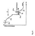
- FIG. 1 is a first embodiment of a memory cell 10 in a three-dimensional view obliquely from above.
- the FIG. 2 shows the corresponding memory cell 10 in cross section.
- the memory cell 10 includes, as will be explained in detail below, a semiconductor structure 11 having a pn junction 12 providing a space charge region.
- a semiconductor structure 11 having a pn junction 12 providing a space charge region.
- the layers forming the pn junction 12 are arranged such that n-doped memory cell material 13 lies below the p-doped memory cell material 14;
- this arrangement is to be understood as an example only:
- the n-doped memory cell material 13 may also be arranged above the p-doped memory cell material 14.
- the substrate 20 On the connection layer 30 is a lower electrical connection 40 of the memory cell 10.
- the substrate 20 consists for example of undoped GaAs and the highly n-doped connection layer 30 of Al x Ga 1-x As.
- connection layer 30 On the connection layer 30 is an n-doped lead layer 50, above which a readout layer 60 is arranged;
- the readout layer 60 is In x Ga 1-x As and provides a 2-dimensional electron gas that is used in the FIG. 2 is indicated by the reference character 2DEG.
- the n-doped lead layer 50 is made of, for example, Al x Ga 1-x As.
- a semiconductor heterostructure 80 which is formed by a carrier layer 90 with nanostructures 100 embedded therein, for example in the form of quantum dots, is provided by a semiconductor intermediate layer 70, for example made of the same material as the feed layer 50, separated from the readout layer 60.
- the band gap of the semiconductor heterostructure 80 is smaller than that in the underlying layer 70 and also smaller than in an overlying n-doped spacer layer 110, so that the semiconductor heterostructure 80 provides at least one potential well in which charge carriers can be trapped.
- the carrier layer 90 is made of, for example, doped or undoped Al x Ga 1-x As, and the nanostructures are preferably formed of In x Ga 1-x Sb or In x Ga 1-x As.
- the n-doped spacer layer 110 may, for example, consist of the same material as the n-doped lead layer 50.
- n-doped spacer layer 110 On the n-doped spacer layer 110 is a highly p-doped terminal layer 120, for example, of the same material as the spacer layer 110, on which an upper electrical terminal 130 of the memory cell 10 rests.
- the transition point between the highly p-doped terminal layer 120 and the n-doped spacer layer 110 forms the pn junction 12.
- a space charge zone is caused in the memory cell 10, the space charge zone width of which to the two electrical Terminals 40 and 130 applied control voltage Us and the doping concentration in the layer 110 and 50 depends.
- FIG. 3 shows the band profile in the memory cell 10 in the event that no voltage or a retention voltage is applied as the control voltage Us, in which the loading state of the memory cell 10 is maintained or kept constant.
- the conduction band E L and electrons are shown as charge carriers; however, the following explanations apply to the valence band and to holes as charge carriers, depending on the design of the semiconductor structure 11.
- the space charge zone width Wn within the n-doped memory cell material 13 is thus greater, at least as large, as the thickness of the layer package, which is composed of the spacer layer 110 and the thickness of the semiconductor hetero-layer 80.
- the charge carriers located within the potential well 200 formed by the semiconductor heterostructure 80 can not leave it because they can not overcome the emission barrier.
- the height of the emission barrier significantly determines the storage time of the storage cell 10 and should therefore be as large as possible; preferably it is at least 1.0 eV in order to realize a storage time of several days.
- FIG. 4 2 shows how the potential well 200 can be filled with charge carriers in order, for example, to write a logical "one" into the memory cell 10.
- a logical one is characterized by a filled potential well 200 and a logical "zero" by an empty potential well;
- this determination is arbitrary and could be the other way around.
- FIG. 5 It is shown how the potential well can be emptied from the charge carriers, for example, to write a logical "zero" in the memory cell 10.
- the band profile is changed or distorted so that a tunnel emission of the electrons trapped in the potential well 200 becomes possible. The electrons can thus leave the potential well 200, whereby it emptied and the memory cell is described with a logical zero.
- the tunneling process is somewhat slower than the relaxation process when the potential well 200 is filled, emptying times or writing times for a logic zero in the nanosecond range are still possible.
- the readout layer 60 is used, the band profile in the FIG. 6 is shown. It can be seen that the band gap in the readout layer 60 is smaller than in the adjacent layers, ie the semiconductor interlayer 70 and the n-doped lead layer 50, so that the already mentioned 2-dimensional electron gas can form in the further potential well 210.
- the readout layer 60 is formed by two lateral connection contacts 250 and 260 (FIG. Fig. 1 and 2 ), so that the electrical properties of the readout layer 60 can be measured with a measuring device 270. Due to the proximity of the readout layer 60 to the semiconductor heterostructure 80, the electrical properties of the readout layer 60 are dependent on the fill state or loading of the potential well 200 in FIG the semiconductor heterostructure 80, so that by measuring the electrical properties of the readout layer 60, the filling state of the potential well 200 can be measured and the memory state of the memory cell 10 can be determined without the risk of changing the memory state of the memory cell 10.
- the loading state of the potential well 200 can be determined by measuring and evaluating the electrical resistance of the readout layer 60 that depends on it.
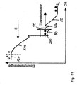
- FIG. 7 shows a second embodiment of a memory cell 10.
- the semiconductor interlayer 70 and the readout layer 60 are missing, so that the semiconductor heterostructure 80 directly adjoins the n-doped lead layer 50.
- the read-out is carried out by evaluating the capacity of the space charge zone Wn of the storage cell 10 which is dependent on the load state of the potential well.
- the read-out can be carried out by evaluating the electrical resistance of the memory cell 10 which is dependent on the load state of the potential well.
- the readout can also be carried out by evaluating the charge transfer dependent on the load state of the potential well 200 from or to the memory cell 10.
- the latter method can be performed both when provided for writing a zero and for unloading Discharges voltage, as well as when the retention voltage applied to the memory cell.
- FIGS. 8 and 9 show a third embodiment of a memory cell 10.
- an auxiliary layer 50a is present which separates the n-doped lead layer 50 from the semiconductor heterostructure 80.
- the n-doped lead layer 50 has a smaller band gap than the auxiliary layer 50a, so that a "tunneling out" of the charge carriers from the potential well 200 during emptying of the semiconductor heterostructure 80 is simplified and thus accelerated.
- the writing of a "zero" is faster because of the auxiliary layer 50a than without this layer.
- the associated band structure shows the FIG. 9 ,
- layers 50a and 110 may be the same material, such as AlAs;
- the layer 50 consists, for example, of 50 percent Al 0.5 Ga 0.5 As.
- the resulting energy level of the emission barrier between the semiconductor heterostructure 80 (eg of GaSb or InSb) and the AlAs barrier 50a in this case would be, for example, about 1 eV or 1.2 eV, resulting in a storage time of days or years at room temperature results.
- there is also a capture barrier in the writing process which, however, is not as high in energy as a flash memory according to the prior art.
- the Figures 10 and 11 show a fourth embodiment for a memory cell 10.
- a quantum well layer 50b is provided which is embedded within the n-doped lead layer 50.
- the quantum well layer 50b has a smaller band gap than the n-doped lead layer 50.
- the quantum well layer 50b may be In x Ga 1-x As embedded in a lead layer 50 of Al x Ga 1-x As matrix material.
- the layer thickness is for example about 1 - 5nm; it makes it possible to increase the extinguishing speed, since discrete energy levels develop within the quantum film layer 50b, which enable resonant tunneling from the semiconductor heterostructure 80 with a corresponding discharge voltage. This means that the charge carriers can more easily tunnel into the conduction or valence band of the lead layer 50 via the states in the quantum well layer 50b than without this layer.
- the Figures 12 and 13 show a fifth embodiment of a memory cell 10.
- an additional delta-shaped doped layer 300 is present, which is arranged within the n-doped lead layer 50 and has a higher doping as the lead layer 50.
- the thickness of the delta-shaped doped layer 300 is preferably a monolayer.
- the function of the delta-shaped doped layer 300 is to provide charge carriers for the formation of the two-dimensional electron gas 2DEG in the readout layer 60 in addition to the feed layer 50.
- the FIG. 14 shows a sixth embodiment of a memory cell 10.
- the layers are arranged such that n-type memory cell material 13 is located above the p-type memory cell material 14.
- an AlAs carrier layer layer 90 For an AlAs carrier layer layer 90, a p-doped feed layer 50, a p-doped spacer layer 110 and InAs as a material for the nanostructures 100, this results in an emission barrier height of at least 0.75 eV and thus storage times of several milliseconds at room temperature.
- an AlAs carrier layer 90 For an AlAs carrier layer 90, a p-doped lead layer 50, a p-doped spacer layer 110 and GaSb as the material for the nanostructures 100, this results in an emission barrier height of at least 1 eV and thus storage times of several days at room temperature.
- an AlAs carrier layer 90 For an AlAs carrier layer 90, a p-doped feed layer 50, a p-doped spacer layer 110 and InSb as the material for the nanostructures 100, this results in an emission barrier height of at least 1.2 eV and thus storage times of several years at room temperature.
- the semiconductor heterostructure 80 may have a plurality of population states, as shown in FIG. 3 is indicated by parallel lines within the potential well 80.
- Each population state can each represent a bit information by being occupied by or left free of charge carriers. This makes it possible to measure the load state of the potential well with an evaluation device in communication with the memory cell and to determine the bit information defined by the load state, for example in the form of a number, using the respective measured value.
Landscapes
- Engineering & Computer Science (AREA)
- Microelectronics & Electronic Packaging (AREA)
- Power Engineering (AREA)
- Physics & Mathematics (AREA)
- Ceramic Engineering (AREA)
- Condensed Matter Physics & Semiconductors (AREA)
- General Physics & Mathematics (AREA)
- Computer Hardware Design (AREA)
- Nanotechnology (AREA)
- Chemical & Material Sciences (AREA)
- Theoretical Computer Science (AREA)
- Crystallography & Structural Chemistry (AREA)
- Mathematical Physics (AREA)
- Semiconductor Memories (AREA)
- Non-Volatile Memory (AREA)
- Static Random-Access Memory (AREA)
Abstract
Description
Die Erfindung bezieht sich auf eine Speicherzelle mit den Merkmalen gemäß dem Oberbegriff des Patentanspruchs 1. Eine derartige Speicherzelle ist aus der Druckschrift:
Die beiden heutzutage wichtigsten kommerziell erhältlichen Halbleiter-Speicherzellen sind DRAM- und Flash-Speicherzellen.The two most important commercially available semiconductor memory cells today are DRAM and flash memory cells.
DRAM-Speicherzellen, die beispielsweise als Arbeitsspeicher in PCs zur Anwendung kommen, speichern die Information als Ladung in einem Kondensator (
Bei Flash-Speicherzellen, die z. B. in Memory-Sticks, Digitalkameras oder Handys eingesetzt werden und gattungsgemäße Speicherzellen bilden, kommt eine MOSFET-Struktur mit einem zusätzlichen Floating-Gate als Speicherelement zum Einsatz (
Den Bandverlauf einer vorbekannten Flash-Speicherzelle zeigt beispielhaft die
Der Erfindung liegt demgemäß die Aufgabe zugrunde, eine Speicherzelle anzugeben, die sich relativ schnell beschreiben lässt und dennoch eine lange Speicherzeit aufweist.The invention is accordingly an object of the invention to provide a memory cell that can be described relatively quickly and yet has a long storage time.
Diese Aufgabe wird erfindungsgemäß durch eine Speicherzelle mit den Merkmalen des Anspruchs 1 und einem Verfahren zum Betreiben einer Speicherzelle nach Anspruch 14 gelöst. Vorteilhafte Ausgestaltungen der Erfindung sind in Unteransprüchen angegeben.This object is achieved by a memory cell having the features of
Danach ist erfindungsgemäß vorgesehen, dass die Speicherzelle eine Halbleiterstruktur mit einer Raumladungszone aufweist und der Potentialtopf durch eine Halbleiterheterostruktur gebildet ist, wobei die Halbleiterheterostruktur und die Raumladungszone relativ zueinander räumlich derart angeordnet sind, dass sich die Halbleiterheterostruktur bei Anliegen der Beibehaltespannung innerhalb der Raumladungszone, bei Anliegen der Einspeisespannung am Rand oder außerhalb der Raumladungszone und bei Anliegen der Entladespannung innerhalb der Raumladungszone befindet.Thereafter, the invention provides that the memory cell has a semiconductor structure with a space charge zone and the potential well is formed by a semiconductor heterostructure, wherein the semiconductor heterostructure and the space charge region relative to each other arranged spatially in that the semiconductor heterostructure is located within the space charge zone when the retention voltage is applied within the space charge zone, when the feed voltage is applied to the edge or outside the space charge zone, and when the discharge voltage is applied.
Ein wesentlicher Vorteil der erfindungsgemäßen Speicherzelle ist darin zu sehen, dass diese aufgrund der erfindungsgemäß vorgesehenen relativen Anordnung zwischen einer Raumladungszone und einer Halbleiterheterostruktur und damit aufgrund des Zusammenspiels zwischen Raumladungszone und Halbleiterheterostruktur sowohl schnell beschrieben werden kann als auch eine sehr lange Speicherzeit aufweist. Die Zugriffszeiten, also die Schreib- oder die Lesezeiten, liegen im Nanosekundenbereich, und gleichzeitig sind Speicherzeiten von mehreren Jahren möglich.An essential advantage of the memory cell according to the invention is the fact that, due to the inventively provided relative arrangement between a space charge zone and a semiconductor heterostructure and thus due to the interaction between the space charge zone and semiconductor heterostructure can be both quickly described and has a very long storage time. The access times, ie the write or read times, are in the nanosecond range, and at the same time storage times of several years are possible.
Die erfindungsgemäße Idee besteht darin, dass sich eine Halbleiterheterostruktur sehr schnell mit Ladungsträgern füllen und auch sehr schnell wieder von diesen befreien lässt, so dass die erwähnte hohe Zugriffsgeschwindigkeit erreicht wird.The idea according to the invention is that a semiconductor heterostructure can fill up very quickly with charge carriers and can also be freed from them very quickly, so that the aforementioned high access speed is achieved.
Die lange Speicherzeit wird erfindungsgemäß dadurch erreicht, dass für den Speicherbetrieb, also für den Zustand des Beibehaltens der Speicherladung, die Raumladungszone auf die Halbleiterheterostruktur ausgeweitet wird, so dass die in der Halbleiterheterostruktur gefangenen Ladungsträger aus dieser nicht entweichen können; gleichzeitig können - und zwar aufgrund der Verarmung an Ladungsträgern innerhalb der Raumladungszone - auch keine anderen Ladungsträger in den Potentialtopf der Halbleiterheterostruktur hineinfallen, so dass der Beladungszustand des Potentialtopfes konserviert wird. Dadurch wird beispielsweise sowohl ein sicheres Speichern einer logischen Eins (zum Beispiel definiert durch einen gefüllten Potentialtopf) als auch ein sicheres Speichern einer logischen Null (zum Beispiel definiert durch einen leeren Potentialtopf) gewährleistet.The long storage time is achieved according to the invention by expanding the space charge zone to the semiconductor heterostructure so that the charge carriers trapped in the semiconductor heterostructure can not escape from it for the storage operation, ie for the state of maintaining the storage charge; At the same time - due to the depletion of charge carriers within the space charge zone - no other charge carriers can fall into the potential well of the semiconductor heterostructure, so that the load state of the potential well is conserved. This ensures, for example, both a secure storage of a logical one (for example defined by a filled potential well) and a safe storage of a logical zero (for example defined by an empty potential well).
Mit anderen Worten besteht der erfinderische Gedanke also darin, eine Raumladungszone mit einer Halbleiterheterostruktur zu verknüpfen, um Bitinformationen zu speichern.In other words, the inventive idea is to combine a space charge zone with a semiconductor heterostructure to store bit information.
Vorzugsweise weist die Halbleiterheterostruktur mindestens eine Nanostruktur auf. Unter Nanostrukturen werden hier beispielsweise niederdimensionale Halbleiterstrukturen verstanden, deren Ausdehnung in eine oder mehrere Raumrichtungen so eingeschränkt ist, dass die Ausdehnung in dieser Raumrichtung in der Größenordnung der "de-Broglie"-Wellenlänge des betrachteten Ladungsträgers (Elektron oder Loch) liegt. Derartige Nanostrukturen können durch Quantenfilme, Quantendrähte oder Quantenpunkte gebildet sein, wie sie beispielsweise aus der Druckschrift "
Die erlaubten Zustände der Nanostrukturen liegen vorzugsweise energetisch tiefer als die des sie umgebenden Materials (z. B. Matrixmaterial). Für die in einer solchen Nanostruktur gebundenen bzw. gespeicherten Ladungsträger liegt in diesem Falle eine Potentialbarriere vor, die die Ladungsträger nur durch eine Energieaufnahme überwinden können, um in das Leitungs- bzw. Valenzband des umgebenden Materials zu gelangen. Ein wesentlicher Vorteil der Nanostrukturen besteht darin, dass zur Darstellung eines Informationsbits nur relativ wenige Ladungsträger erforderlich sind, weil die Anzahl an verfügbaren Besetzungszuständen innerhalb des Potentialtopfes bei Nanostrukturen sehr klein ist: Im Idealfall kann ein Informationsbit mit nur einem oder zwei Ladungsträgern dargestellt werden. Speicherzellen mit Nanostrukturen unterscheiden sich damit erheblich von den eingangs beschriebenen vorbekannten Speicherzellentypen, bei denen zur Speicherung eines Informationsbits eine große Anzahl von Ladungsträgern benötigt wird und sich ein relativ hoher Energieverbrauch beim Schreib- und Löschprozess ergibt: Flash-Speicherzellen benötigen beispielsweise ca. eintausend Elektronen, während DRAM-Speicherzellen für ein Informationsbit sogar mehrere zehntausend Ladungsträger brauchen.The allowed states of the nanostructures are preferably lower in energy than those of the surrounding material (eg matrix material). For the charge carriers bound or stored in such a nanostructure, there is in this case a potential barrier which the charge carriers can only overcome by absorbing energy in order to reach the conduction or valence band of the surrounding material. A significant advantage of the nanostructures is that only a relatively small number of charge carriers are required to represent an information bit because the number of available population states within the potential well of nanostructures is very small. Ideally, an information bit can be represented with only one or two charge carriers. Memory cells with nanostructures thus differ significantly from the previously described prior art memory cell types in which a large number of charge carriers are required for storing an information bit and a relatively high energy consumption results in the write and erase process: Flash memory cells need for example, about one thousand electrons, while DRAM memory cells for an information bit even need tens of thousands of charge carriers.
Vorzugsweise ist die Speicherzelle derart ausgestaltet, dass sich der Beladungszustand der Halbleiterheterostruktur durch Anlegen einer Durchlassspannung an die Anschlüsse vergrößern lässt und eine Vergrößerung des Beladungszustandes durch Relaxation der Ladungsträger von einer an die Halbleiterheterostruktur mittelbar oder unmittelbar angrenzenden Leitungs- oder Valenzbandkante eines dotierten Halbleitermaterials erfolgt, weil nämlich ein Relaxationsvorgang physikalisch sehr schnell abläuft.Preferably, the memory cell is configured in such a way that the loading state of the semiconductor heterostructure can be increased by applying a forward voltage to the terminals and increasing the charge state by relaxation of the charge carriers from a conduction or valence band edge of a doped semiconductor material directly or indirectly adjacent to the semiconductor heterostructure, because namely a relaxation process is physically very fast.
Der Bandverlauf ist im Bereich der Halbleiterheterostruktur beispielsweise derart ausgebildet, dass der Beladungszustand der Halbleiterheterostruktur durch Anlegen einer Sperrspannung verringerbar ist und dass die Verringerung des Beladungszustandes kann beispielsweise auf einem Tunneleffekt beruhen.The band profile is formed in the region of the semiconductor heterostructure, for example, in such a way that the loading state of the semiconductor heterostructure can be reduced by applying a blocking voltage and that the reduction of the loading state can be based, for example, on a tunneling effect.
Die Halbleiterstruktur kann beispielsweise aus einer III/V-Materialkombination, einer II/VI-Materialkombination oder aus einer IV/IV-Materialkombination bestehen.The semiconductor structure can consist, for example, of a III / V material combination, of an II / VI material combination or of an IV / IV material combination.
Zum Auslesen der Speicherzelle kann beispielsweise eine ein 2-dimensionales Elektronengas enthaltende Ausleseschicht vorhanden sein. Vorzugsweise ist eine solche Ausleseschicht von der Halbleiterheterostruktur durch eine Halbleiterzwischenschicht getrennt. Die Dicke der Halbleiterzwischenschicht ist beispielsweise derart bemessen, dass die Ausleseschicht im Speicherzustand am Rand oder außerhalb der Raumladungszone liegt und die Dicke der Halbleiterzwischenschicht beträgt mindestens 5 nm.For reading out the memory cell, for example, a readout layer containing a 2-dimensional electron gas may be present. Preferably, such a readout layer is separated from the semiconductor heterostructure by a semiconductor interlayer. The thickness of the semiconductor interlayer, for example, is dimensioned such that the readout layer in the memory state at the edge or outside the space charge zone and the thickness of the semiconductor interlayer is at least 5 nm.
Besonders bevorzugt ist die Halbleiterheterostruktur durch eine Trägerschicht gebildet, in der eine Mehrzahl a Nanostrukturen beabstandet voneinander angeordnet ist und dass das Schichtmaterial der Trägerschicht einen höheren elektrischen Widerstand aufweist als die Ausleseschicht. Dadurch, dass die Nanostrukturen beabstandet voneinander angeordnet sind, ist es möglich, Anschlusskontakte zum elektrischen Kontaktieren der Ausleseschicht ohne weitere Isolationsschichten durch die Halbleiterheterostruktur hindurchzuführen, ohne dass es zu einem unmittelbaren Kurzschluss zwischen den Nanostrukturen kommen kann.The semiconductor heterostructure is particularly preferably formed by a carrier layer in which a plurality of nanostructures is arranged at a distance from each other and in that the layer material of the carrier layer has a higher electrical resistance than the readout layer. Because the nanostructures are arranged at a distance from one another, it is possible to pass through connection contacts for electrically contacting the readout layer without further insulation layers through the semiconductor heterostructure, without the possibility of an immediate short circuit between the nanostructures.
Im Hinblick auf eine besonders große Informationsdichte wird es als vorteilhaft angesehen, wenn die Halbleiterheterostruktur eine Mehrzahl an Besetzungszuständen aufweist, die jeweils eine Bitinformation repräsentieren und von Ladungsträgern besetzt werden können, und dass die Anzahl der besetzten Besetzungszustände auslesbar ist. In dieser Weise lassen sich Ladungsträgermultiplexing und damit Multi-Level-Zellen realisieren.With regard to a particularly high information density, it is considered advantageous if the semiconductor heterostructure has a plurality of population states, each of which represents bit information and can be occupied by charge carriers, and that the number of occupied population states is readable. In this way, charge carrier multiplexing and thus multi-level cells can be realized.
Mit der Speicherzelle kann beispielsweise eine Auswerteeinrichtung in Verbindung stehen, die den Beladungszustand des zumindest einem Potentialtopfes misst und mit dem Messwert eine die Bitinformation angebende Zahl ermittelt.For example, an evaluation device can be in communication with the memory cell, which measures the load state of the at least one potential well and determines a number indicating the bit information with the measured value.
Beispielsweise kann die Auswerteeinrichtung als Bitinformation eine binäre Zahl ausgeben.For example, the evaluation device can output a binary number as bit information.
Die Erfindung bezieht sich außerdem auf ein Verfahren zum Betreiben einer Speicherzelle, bei dem eine Bitinformation der Speicherzelle durch den Beladungszustand mindestens eines Potentialtopfes der Speicherzelle festgelegt wird, wobei durch Anlegen einer elektrischen Einspeisespannung an die Speicherzelle der Beladungszustand des Potentialtopfes mit Ladungsträgern vergrößert und durch Anlegen einer Entladespannung verkleinert wird und wobei bei Anlegen einer Beibehaltespannung die Ladungsträger innerhalb des Potentialtopfes gefangen bleiben. Ein solches Verfahren ist von den eingangs erwähnten Flash-Speicherzellen her bekannt.The invention also relates to a method for operating a memory cell in which a bit information of the memory cell is determined by the loading state of at least one potential well of the memory cell, wherein by applying an electrical supply voltage to the memory cell, the loading state of the potential well with charge carriers increased and by applying a Discharging voltage is reduced and wherein upon application of a retention voltage, the charge carriers remain trapped within the potential well. Such a method is known from the flash memory cells mentioned above.
Im Hinblick auf eine schnelle Zugriffszeit und eine lange Speicherzeit wird erfindungsgemäß vorgeschlagen, dass zum Vergrößern des Beladungszustandes eine derartige Einspeisespannung an die Speicherzelle angelegt wird, dass sich eine den Potentialtopf bildende Halbleiterheterostruktur am Rand oder außerhalb einer Raumladunsgzone der Speicherzelle befindet, dass zum Beibehalten des Beladungszustandes eine derartige Beibehaltespannung an die Speicherzelle angelegt wird, dass sich die Halbleiterheterostruktur innerhalb dieser Raumladungszone befindet und die Ladungsträger innerhalb der Halbleiterheterostruktur gefangen sind, und dass zum Verkleinern des Beladungszustandes eine derartige Entladespannung an die Speicherzelle angelegt wird, dass sich die Halbleiterheterostruktur innerhalb dieser Raumladungszone befindet, jedoch die Ladungsträger die Heterostruktur verlassen können.With regard to a fast access time and a long storage time, the invention proposes that to increase the loading state, such a supply voltage is applied to the memory cell, that is a potential well-forming semiconductor heterostructure at the edge or outside a Raumladunsgzone the memory cell is that to maintain the loading state applying a retention voltage to the memory cell such that the semiconductor heterostructure is within that space charge region and the charge carriers are trapped within the semiconductor heterostructure, and such that a discharge voltage is applied to the memory cell to reduce the charge state such that the semiconductor heterostructure is within that space charge region; however, the charge carriers can leave the heterostructure.
Bezüglich der Vorteile des erfindungsgemäßen Verfahrens sei auf die obigen Ausführungen im Zusammenhang mit der erfindungsgemäßen Speicherzelle verwiesen, weil die Vorteile der erfindungsgemäßen Speicherzelle denen des erfindungsgemäßen Verfahrens im Wesentlichen entsprechen. Entsprechendes gilt für vorteilhafte Weiterbildungen des erfindungsgemäßen Verfahrens.With regard to the advantages of the method according to the invention, reference is made to the above statements in connection with the memory cell according to the invention, because the advantages of the memory cell according to the invention essentially correspond to those of the method according to the invention. The same applies to advantageous developments of the method according to the invention.
Das Auslesen kann beispielsweise durchgeführt werden, indem ein vom Beladungszustand des Potentialtopfes abhängiger elektrischer Widerstand einer ein 2-dimensionales Elektronengas enthaltenden Ausleseschicht ausgewertet wird und zumThe reading can be carried out, for example, by evaluating a load state of the potential well dependent electrical resistance of a 2-dimensional electron gas containing readout layer and the
Vergrößern des Beladungszustandes des Potentialtopfes wird bevorzugt eine derartige Einspeisespannung an die Speicherzelle angelegt, dass die Ladungsträger von einer an den Potentialtopf mittelbar oder unmittelbar angrenzenden Leitungs oder Valenzbandkante eines dotierten Halbleitermaterials in den Potentialtopf relaxieren und zumTo increase the loading state of the potential well, such a supply voltage is preferably applied to the memory cell such that the charge carriers relax into the potential well from a line or valence band edge of a doped semiconductor material that is directly or indirectly adjacent to the potential well
Verringern des Beladungszustandes des Potentialtopfes wird eine derartige Entladespannung an die Speicherzelle angelegt, dass die Ladungsträger aus dem Potentialtopf heraustunneln.Decreasing the loading state of the potential well, such a discharge voltage is applied to the memory cell that tunnel out the charge carriers from the potential well.
Die Erfindung wird nachfolgend anhand von Ausführungsbeispielen näher erläutert; dabei zeigen beispielhaft
- Figuren 1-2
- ein erstes Ausführungsbeispiel für eine er- findungsgemäße Speicherzelle mit einer Na- nostruktur (beispielsweise einem Quanten- film), die einen Potentialtopf bildet, oder mehrere Nanostrukturen (beispielsweise Quantenpunkte) die mehrere Potentialtöpfe bilden, sowie mit einer Ausleseschicht,
- Figuren 3-5
- den Bandverlauf innerhalb der Speicherzelle gemäß der
Figur 1 - Figur 6
- den Einfluss der Ausleseschicht auf den Bandverlauf,
- Figur 7
- ein zweites Ausführungsbeispiel für eine erfindungsgemäße Speicherzelle mit Na- nostrukturen, jedoch ohne Ausleseschicht,
- Figuren 8-9
- ein drittes Ausführungsbeispiel für eine erfindungsgemäße Speicherzelle ohne Ausle- seschicht, jedoch mit einer zusätzlichen Hilfsschicht für ein verbessertes Tunnel- verhalten beim Entleeren des Potentialtop- fes;
- Figuren 10-11
- ein viertes Ausführungsbeispiel für eine erfindungsgemäße Speicherzelle mit einer zusätzlichen Quantenfilmschicht für ein verbessertes Tunnelverhalten beim Entleeren des Potentialtopfes,
- Figuren 12-13
- ein fünftes Ausführungsbeispiel für eine Speicherzelle 10 mit einer zusätzlichen deltaförmig dotierten Schicht,
Figur 14- ein sechstes Ausführungsbeispiel mit einem gegenüber den Ausführungsbeispielen 1-5 in- versen Dotierungsprofil und
- Figur 15
- zur allgemeinen Erläuterung eine Flash- Speicherzelle nach dem Stand der Technik.
- Figures 1-2
- a first exemplary embodiment of a memory cell according to the invention having a nanostructure (for example a quantum film) which forms a potential well, or a plurality of nanostructures (for example quantum dots) which form a plurality of potential wells, and having a readout layer,
- Figures 3-5
- the band profile within the memory cell according to the
FIG. 1 while maintaining the filling state of the potential well, when filling the potential well and when emptying the potential well, - FIG. 6
- the influence of the readout layer on the band history,
- FIG. 7
- A second exemplary embodiment of a memory cell according to the invention with nanostructures, but without a readout layer,
- FIGS. 8-9
- a third embodiment of a memory cell according to the invention without Ausle- seschicht, but with an additional auxiliary layer for improved tunnel behavior when emptying the Potentialtop- fes;
- Figures 10-11
- A fourth exemplary embodiment of a memory cell according to the invention with an additional quantum-film layer for improved tunnel behavior when emptying the potential well,
- FIGS. 12-13
- A fifth embodiment of a
memory cell 10 with an additional delta-shaped doped layer, - FIG. 14
- a sixth embodiment with a comparison with the embodiments 1-5 inverse doping profile and
- FIG. 15
- for general explanation, a flash memory cell according to the prior art.
In den
In der
Die Speicherzelle 10 enthält, wie weiter unten im Detail erläutert werden wird, eine Halbleiterstruktur 11 mit einem pn-Übergang 12, der eine Raumladungszone bereitstellt. Bei dem nachfolgend beschriebenen Ausführungsbeispiel wird davon ausgegangen, dass die den pn-Übergang 12 bildenden Schichten so angeordnet sind, dass n-dotiertes Speicherzellenmaterial 13 unterhalb des p-dotierten Speicherzellenmaterials 14 liegt; selbstverständlich ist diese Anordnung nur beispielhaft zu verstehen: So kann das n-dotierte Speicherzellenmaterial 13 stattdessen auch oberhalb des p-dotierten Speicherzellenmaterials 14 angeordnet werden.The
Man erkennt in den beiden
Auf der Anschlussschicht 30 liegt eine n-dotierte Zuleitungsschicht 50 auf, oberhalb derer eine Ausleseschicht 60 angeordnet ist; die Ausleseschicht 60 besteht beispielsweise aus InxGa1-xAs und stellt ein 2-dimensionales Elektronengas zur Verfügung, das in der
Durch eine Halbleiterzwischenschicht 70 beispielsweise aus demselben Material wie die Zuleitungsschicht 50 von der Ausleseschicht 60 getrennt ist eine Halbleiterheterostruktur 80 vorgesehen, die durch eine Trägerschicht 90 mit darin eingebetteten Nanostrukturen 100, beispielsweise in Form von Quantenpunkten, gebildet ist. Der Bandabstand der Halbleiterheterostruktur 80 ist kleiner als der in der darunter liegenden Schicht 70 sowie ebenfalls kleiner als in einer darüber befindlichen n-dotierten Abstandsschicht 110, so dass die Halbleiterheterostruktur 80 mindestens einen Potentialtopf bereitstellt, in dem Ladungsträger gefangen werden können.A
Die Trägerschicht 90 besteht beispielsweise aus dotiertem oder undotiertem AlxGa1-xAs, und die Nanostrukturen werden vorzugsweise aus InxGa1-xSb oder InxGa1-xAs gebildet. Die n-dotierte Abstandsschicht 110 kann beispielsweise aus demselben Material wie die n-dotierte Zuleitungsschicht 50 bestehen.The
Auf der n-dotierten Abstandsschicht 110 befindet sich eine hoch p-dotierte Anschlussschicht 120 beispielsweise aus demselben Material wie die Abstandsschicht 110, auf der ein oberer elektrischer Anschluss 130 der Speicherzelle 10 aufliegt.On the n-doped
Durch die Übergangsstelle zwischen der hoch p-dotierten Anschlussschicht 120 und der n-dotierten Abstandsschicht 110 wird der pn-Übergang 12 gebildet. Durch den pn-Übergang 12 wird in der Speicherzelle 10 eine Raumladungszone hervorgerufen, deren Raumladungszonenweite von der an die beiden elektrischen Anschlüsse 40 und 130 angelegten Steuerspannung Us und der Dotierkonzentration in der Schicht 110 und 50 abhängt.The transition point between the highly p-doped
Die
Es lässt sich in der
In der
Aufgrund der räumlichen Lage des Potentialtopfes 200 innerhalb der Raumladungszone Wn wird außerdem sichergestellt, dass keine zusätzlichen Ladungsträger unerwünscht in den Potentialtopf 200 hineinfallen können und den Speicherzustand in dieser Weise verändern bzw. überschreiben können; denn die Raumladungszone ist sehr arm an freien Ladungsträgern, so dass schlicht keine Ladungsträger für eine Verfälschung des Speicherinhalts zur Verfügung stehen. Von außerhalb der Raumladungszone Wn können ebenfalls keine Ladungsträger in den Potentialtopfs 200 eindringen, weil sie die Einfangbarriere, die durch den Bandverlauf innerhalb der Raumladungszone gebildet wird, nicht überwinden können.Due to the spatial position of the
In der
Zum "Schreiben" einer logischen Eins wird an die beiden Anschlüsse 40 und 130 und damit an den pn-Übergang 12 als Steuerspannung Us eine Einspeisespannung Uspeis, und zwar eine Durchlassspannung Uspeis > Umin (Umin beträgt beispielsweise 0,7 V), angelegt, so dass die Raumladungszone Wn verkleinert wird. Man erkennt in der
In der
Der Tunnelvorgang ist zwar etwas langsamer als der Relaxationsvorgang beim Befüllen des Potentialtopfes 200, jedoch sind dennoch Entleerungszeiten bzw. Schreibzeiten für eine logische Null im Nanosekundenbereich möglich.Although the tunneling process is somewhat slower than the relaxation process when the
Im Zusammenhang mit den
Die Ausleseschicht 60 ist durch zwei seitliche Anschlusskontakte 250 und 260 (
Beispielsweise kann der Beladungszustand des Potentialtopfs 200 bestimmt werden, indem der von diesem abhängige elektrische Widerstand der Ausleseschicht 60 gemessen und ausgewertet wird.For example, the loading state of the
Die
Während das Schreiben von logischen Einsen und Nullen genauso ablaufen kann, wie dies im Zusammenhang mit den
Beispielsweise wird das Auslesen durchgeführt, indem die vom Beladungszustand des Potentialtopfes abhängige Kapazität der -Raumladungszone Wn der Speicherzelle 10 ausgewertet wird. Alternativ kann das Auslesen durchgeführt werden, indem der vom Beladungszustand des Potentialtopfes abhängige elektrische Widerstand der Speicherzelle 10 ausgewertet wird.For example, the read-out is carried out by evaluating the capacity of the space charge zone Wn of the
Auch kann das Auslesen durchgeführt werden, indem der vom Beladungszustand des Potentialtopfes 200 abhängige Ladungstransfer von oder zu der Speicherzelle 10 ausgewertet wird. Das letztgenannte Verfahren kann sowohl durchgeführt werden, wenn die zum Schreiben einer Null bzw. zum Entladen vorgesehene Entladespannung anliegt, als auch dann, wenn die Beibehaltespannung an der Speicherzelle anliegt.The readout can also be carried out by evaluating the charge transfer dependent on the load state of the
Die
Die Schichten 50a und 110 können beispielsweise aus demselben Material bestehen, beispielsweise aus AlAs; die Schicht 50 besteht beispielsweise aus 50-prozentigem Al0.5Ga0.5As. Die resultierende energetische Höhe der Emissionsbarriere zwischen der Halbleiterheterostruktur 80 (z.B. aus GaSb oder InSb) und der AlAs-Barriere 50a würde in diesem Fall beispielsweise bei ungefähr 1 eV oder 1,2 eV liegen, wodurch sich eine Speicherzeit von Tagen bzw. Jahren bei Raumtemperatur ergibt. Aufgrund dieser Schichtanordnung ergibt sich zusätzlich auch eine Einfang Barriere beim Schreibprozess, die energetisch aber bei weitem nicht so hoch wie einem Flash-Speicher nach dem Stand der Technik ist.For example, layers 50a and 110 may be the same material, such as AlAs; The
Die
Die
Die
Zusammenfassend sei erwähnt, dass grundsätzlich alle Arten von Halbleitermaterialien bzw. Halbleiterstrukturen eingesetzt werden können, mit denen sich Halbleiterheterostrukturen mit Potentialtöpfen bilden lassen. Besonders geeignet sind jedoch folgende Materialkombinationen: Für eine Al0,43Ga0,57As Trägerschicht 90, eine n-dotierte Zuleitungsschicht 50, eine n-dotierte Abstandsschicht 110 und InAs als Material für die Nanostrukturen 100 ergeben sich eine Emissionsbarrierenhöhe von circa mindestens 0,7 eV und damit Speicherzeiten bei Raumtemperatur von mehreren Millisekunden.In summary, it should be mentioned that basically all types of semiconductor materials or semiconductor structures can be used, with which semiconductor heterostructures can be formed with potential wells. However, the following material combinations are particularly suitable: For an Al 0.43 Ga 0.57 As
Für eine AlAs Trägerschichtschicht 90,eine p-dotierte Zuleitungsschicht 50, eine p-dotierte Abstandsschicht 110 und InAs als Material für die Nanostrukturen 100 ergeben sich eine Emissionsbarrierenhöhe von mindestens 0,75 eV und damit Speicherzeiten von mehreren Millisekunden bei Raumtemperatur.For an AlAs
Für eine AlAs Trägerschicht 90, eine p-dotierte Zuleitungsschicht 50, eine p-dotierte Abstandsschicht 110 und GaSb als Material für die Nanostrukturen 100 ergeben sich eine Emissionsbarrierenhöhe von mindestens 1 eV und damit Speicherzeiten von mehreren Tagen bei Raumtemperatur.For an AlAs
Für eine AlAs Trägerschicht 90, eine p-dotierte Zuleitungsschicht 50, eine p-dotierte Abstandsschicht 110 und InSb als Material für die Nanostrukturen 100 ergeben sich eine Emissionsbarrierenhöhe von mindestens 1,2 eV und damit Speicherzeiten von mehreren Jahren bei Raumtemperatur.For an AlAs
Auch ist zu erwähnen, dass die Halbleiterheterostruktur 80 ein ist Mehrzahl an Besetzungszuständen aufweisen kann, wie dies in der
- 1010
- Speicherzellememory cell
- 1111
- HalbleiterstrukturSemiconductor structure
- 1212
- pn-Übergangpn junction
- 1313
- n-dotiertes Speicherzellenmaterialn-doped memory cell material
- 1414
- p-dotiertes Speicherzellenmaterialp-doped memory cell material
- 2020
- Substratsubstratum
- 3030
- hoch n-dotierte Anschlussschichthighly n-doped terminal layer
- 4040
- unterer elektrischer Anschlusslower electrical connection
- 5050
- n-dotierte Zuleitungsschichtn-doped lead layer
- 50a50a
- Hilfsschichtauxiliary layer
- 50b50b
- QuantenfilmschichtQuantum well layer
- 6060
- Ausleseschichtreadout layer
- 7070
- HalbleiterzwischenschichtIntermediate semiconductor layer
- 8080
- HalbleiterheterostrukturSemiconductor heterostructure
- 9090
- Trägerschichtbacking
- 100100
- Nanostrukturennanostructures
- 110110
- n-dotierte Abstandsschichtn-doped spacer layer
- 120120
- hoch p-dotierte Anschlussschichthighly p-doped terminal layer
- 130130
- oberer elektrischer Anschlussupper electrical connection
- 200200
- Potentialtopfpotential well
- 210210
- weiterer Potentialtopffurther potential well
- 250, 260250, 260
- seitliche Anschlusskontaktelateral connection contacts
- 300300
- deltaförmig dotierte Schichtdelta-shaped doped layer
- USUS
- Steuerspannungcontrol voltage
- WnWn
- RaumladungszonenweiteSpace charge zone width
Claims (15)
- Memory cell (10) for storing at least one item of bit information, wherein the memory cell comprises a semiconductor structure (11) with a band profile (EL) having at least one potential well (200) and comprises at least two electrical connections (40, 130),- wherein the charged state of the potential well with charge carriers can be increased by applying an electrical supply voltage (Us=Usupply) to the two connections, can be reduced by applying a discharge voltage (Us=Urev), and can be maintained by applying a maintaining voltage (Us=Umaint), and- wherein the respective charged state of the potential well defines the item of bit information of the memory cell,- wherein the semiconductor structure has a space charge zone (Wn), and- wherein the potential well is formed by a semiconductor heterostructure (80),
characterized in that- the semiconductor heterostructure and the space charge zone are spatially arranged relative to one another in such a way that the semiconductor heterostructure is situated within the space charge zone when the maintaining voltage is present, at the edge of or outside the space charge zone when the supply voltage is present, and within the space charge zone when the discharge voltage is present. - Memory cell according to Claim 1, characterized in that the semiconductor heterostructure has at least one nanostructure (100).
- Memory cell according to Claim 1 or 2, characterized- in that the charged state of the semiconductor heterostructure can be increased by applying a forward voltage to the connections, and- in that the charged state is increased by relaxation of the charge carriers from a conduction or valence band edge of a doped semiconductor material that is indirectly or directly adjacent to the semiconductor heterostructure.
- Memory cell according to any of the preceding claims, characterized- in that the band profile is embodied in the region of the semiconductor heterostructure in such a way that the charged state of the semiconductor heterostructure can be reduced by applying a reverse voltage to the connections, and- in that the reduction of the charged state is based on a tunnel effect by means of which the charge carriers leave the semiconductor heterostructure.
- Memory cell according to any of the preceding claims, characterized in that the semiconductor structure comprises a III/V material combination, a II/VI material combination or a IV/IV material combination.
- Memory cell according to any of the preceding claims, characterized in that a read-out layer (60) containing a two-dimensional electron gas (2DEG) is present, which enables the item of bit information of the memory cell to be read out.
- Memory cell according to Claim 6, characterized in that the read-out layer is separated from the semiconductor heterostructure by a semiconductor interlayer (70).
- Memory cell according to Claim 7, characterized- in that the thickness of the semiconductor interlayer is dimensioned in such a way that the read-out layer lies at the edge of or outside the space charge zone in the storage state, and- in that the thickness of the semiconductor interlayer is at least 5 nm.
- Memory cell according to any of the preceding claims, characterized- in that the semiconductor heterostructure is formed by a carrier layer (90) in which a plurality of nanostructures (100) are arranged at a distance from one another, and- in that the layer material of the carrier layer has a higher electrical resistance than the read-out layer.
- Memory cell according to Claim 9, characterized in that connection contacts (250, 260) for making electrical contact with the read-out layer are led through the semiconductor heterostructure.
- Memory cell according to any of the preceding claims, characterized in that the semiconductor heterostructure has a plurality of occupation states which each represent an item of bit information by virtue of the fact that they can be occupied by charge carriers, and in that the number of occupied occupation states can be read out.
- Memory device having at least one memory cell according to any of the preceding claims, characterized in that an evaluation device is connected to the memory cell, which evaluation device measures the charged state of the at least one potential well and, with the measured value, determines a number indicating the item of bit information.
- Memory device according to Claim 12, characterized in that the evaluation device outputs a binary number as bit information.
- Method for operating a memory cell (10), in which an item of bit information of the memory cell is defined by the charged state of at least one potential well (200) of the memory cell,- wherein the charged state of the potential well with charge carriers is increased by applying an electrical supply voltage (Us=Usupply) to the memory cell, and is reduced by applying a discharge voltage (Us=Urev), and- wherein the charge carriers remain trapped within the potential well upon application of a maintaining voltage (Us=Umaint),
characterized- in that for increasing the charged state, a supply voltage is applied to the memory cell which is such that a semiconductor heterostructure (80) forming the potential well is situated at the edge of or outside a space charge zone (Wn) of the memory cell,- in that, for maintaining the charged state, a maintaining voltage is applied to the memory cell which is such that the semiconductor heterostructure is situated within said space charge zone, and- in that, for reducing the charged state, a discharge voltage is applied to the memory cell which is such that the semiconductor heterostructure is situated within said space charge zone, but the charge carriers can leave the heterostructure. - Method according to Claim 14, characterized- in that the read-out is carried out by reading a read-out layer containing a two-dimensional electron gas, by evaluating the electrical resistance of said read-out layer, said electrical resistance being dependent on the charged state of the potential well,- in that, for increasing the charged state of the potential well, a supply voltage is applied to the memory cell which is such that the charge carriers relax into the potential well from a conduction or valence band edge of a doped semiconductor material that is indirectly or directly adjacent to the potential well, and- in that, for reducing the charged state of the potential well, a discharge voltage is applied to the memory cell which is such that the charge carriers tunnel out of the potential well.
Applications Claiming Priority (2)
| Application Number | Priority Date | Filing Date | Title |
|---|---|---|---|
| DE102006059110A DE102006059110A1 (en) | 2006-12-08 | 2006-12-08 | Memory cell and method for storing data |
| PCT/DE2007/002182 WO2008067799A2 (en) | 2006-12-08 | 2007-12-03 | Memory cell, and method for storing data |
Publications (2)
| Publication Number | Publication Date |
|---|---|
| EP2097904A2 EP2097904A2 (en) | 2009-09-09 |
| EP2097904B1 true EP2097904B1 (en) | 2011-06-15 |
Family
ID=39361416
Family Applications (1)
| Application Number | Title | Priority Date | Filing Date |
|---|---|---|---|
| EP07846385A Active EP2097904B1 (en) | 2006-12-08 | 2007-12-03 | Memory cell, and method for storing data |
Country Status (7)
| Country | Link |
|---|---|
| US (1) | US7948822B2 (en) |
| EP (1) | EP2097904B1 (en) |
| JP (1) | JP5521142B2 (en) |
| KR (1) | KR101436663B1 (en) |
| AT (1) | ATE513297T1 (en) |
| DE (1) | DE102006059110A1 (en) |
| WO (1) | WO2008067799A2 (en) |
Families Citing this family (4)
| Publication number | Priority date | Publication date | Assignee | Title |
|---|---|---|---|---|
| KR101642932B1 (en) * | 2009-11-02 | 2016-07-27 | 삼성전자주식회사 | Local self-boosting method of flash memory device and program method using the same |
| US8331142B2 (en) * | 2010-12-16 | 2012-12-11 | Technische Universitat Berlin | Memory |
| DE102011006782A1 (en) * | 2011-04-05 | 2012-10-11 | Technische Universität Berlin | memory cell |
| US9542990B2 (en) * | 2012-02-13 | 2017-01-10 | Institute of Microelectronics, Chinese Academy of Sciences | Semiconductor memory device and method for accessing the same |
Family Cites Families (20)
| Publication number | Priority date | Publication date | Assignee | Title |
|---|---|---|---|---|
| US3387286A (en) | 1967-07-14 | 1968-06-04 | Ibm | Field-effect transistor memory |
| JPS5840855A (en) * | 1981-09-04 | 1983-03-09 | Hitachi Ltd | Semiconductor memory cell |
| JPS63239867A (en) * | 1987-03-27 | 1988-10-05 | Nippon Telegr & Teleph Corp <Ntt> | Semiconductor memory cell |
| DE3737572A1 (en) | 1987-11-05 | 1989-05-24 | Licentia Gmbh | Controllable quantum pot structure |
| US4905063A (en) * | 1988-06-21 | 1990-02-27 | American Telephone And Telegraph Company, At&T Bell Laboratories | Floating gate memories |
| EP0535293A1 (en) | 1991-01-29 | 1993-04-07 | Max-Planck-Gesellschaft zur Förderung der Wissenschaften e.V. | A method of fabricating a compositional semiconductor device |
| JP3361135B2 (en) | 1991-12-20 | 2003-01-07 | テキサス インスツルメンツ インコーポレイテツド | Quantum effect logic unit and manufacturing method thereof |
| US5798539A (en) | 1992-12-10 | 1998-08-25 | Daimler Benz Ag | Bipolar transistor for very high frequencies |
| US5614435A (en) | 1994-10-27 | 1997-03-25 | The Regents Of The University Of California | Quantum dot fabrication process using strained epitaxial growth |
| JP3320641B2 (en) | 1996-09-13 | 2002-09-03 | 株式会社東芝 | Memory cell |
| US6060723A (en) | 1997-07-18 | 2000-05-09 | Hitachi, Ltd. | Controllable conduction device |
| US6054349A (en) | 1997-06-12 | 2000-04-25 | Fujitsu Limited | Single-electron device including therein nanocrystals |
| JP2000040753A (en) * | 1998-07-24 | 2000-02-08 | Sony Corp | Memory device |
| GB2341722B (en) * | 1998-09-16 | 2001-01-17 | Toshiba Res Europ Ltd | An optical semiconductor device |
| KR100360496B1 (en) | 2000-04-15 | 2002-11-13 | 삼성전자 주식회사 | Double value single electron memory using multi-quantum dot and driving method thereof |
| KR100347146B1 (en) | 2000-08-31 | 2002-08-03 | 주식회사 하이닉스반도체 | Method for fabricating quantum dot and single electron memory device using the quantum dot |
| US6753273B2 (en) | 2001-07-31 | 2004-06-22 | The Board Of Trustees Of The University Of Illinois | Semiconductor devices and methods |
| DE10158018A1 (en) | 2001-11-27 | 2003-06-12 | Infineon Technologies Ag | Layer arrangement and method for operating a layer arrangement as data storage |
| KR100459895B1 (en) | 2002-02-09 | 2004-12-04 | 삼성전자주식회사 | Memory device with quantum dot and method of manufacturing the same |
| JP4997464B2 (en) | 2004-01-16 | 2012-08-08 | 国立大学法人 千葉大学 | Quantum point contact, quantum dot, quantum wire, memory device, and quantum computer |
-
2006
- 2006-12-08 DE DE102006059110A patent/DE102006059110A1/en not_active Withdrawn
-
2007
- 2007-12-03 EP EP07846385A patent/EP2097904B1/en active Active
- 2007-12-03 KR KR1020097014186A patent/KR101436663B1/en active IP Right Grant
- 2007-12-03 US US12/518,223 patent/US7948822B2/en active Active
- 2007-12-03 JP JP2009539602A patent/JP5521142B2/en active Active
- 2007-12-03 WO PCT/DE2007/002182 patent/WO2008067799A2/en active Application Filing
- 2007-12-03 AT AT07846385T patent/ATE513297T1/en active
Also Published As
| Publication number | Publication date |
|---|---|
| KR20090104019A (en) | 2009-10-05 |
| WO2008067799A3 (en) | 2008-07-31 |
| KR101436663B1 (en) | 2014-09-01 |
| JP5521142B2 (en) | 2014-06-11 |
| WO2008067799A2 (en) | 2008-06-12 |
| EP2097904A2 (en) | 2009-09-09 |
| JP2010512012A (en) | 2010-04-15 |
| DE102006059110A1 (en) | 2008-06-12 |
| US7948822B2 (en) | 2011-05-24 |
| US20100080068A1 (en) | 2010-04-01 |
| ATE513297T1 (en) | 2011-07-15 |
Similar Documents
| Publication | Publication Date | Title |
|---|---|---|
| DE4020007C2 (en) | Non-volatile memory | |
| EP0783180B1 (en) | Electrically programmable memory cell arrangement and process for making the same | |
| DE102004050641A1 (en) | Charge-trapping memory cell | |
| DE10155416A1 (en) | Permanent semiconductor storage | |
| DE2409568A1 (en) | SEMICONDUCTOR STORAGE ELEMENT | |
| DE102019116876A1 (en) | ASYNCHRONOUS READING CIRCUIT USING DELAY SCAN IN MAGNETORESISTIVE DIRECT ACCESS MEMORY (MRAM) | |
| DE102004006505A1 (en) | Charge trapping memory cell and manufacturing process | |
| EP2097904B1 (en) | Memory cell, and method for storing data | |
| DE102008021396A1 (en) | memory cell | |
| DE2201028C3 (en) | Method for operating a field effect transistor and field effect transistor for carrying out this method | |
| DE2432352C3 (en) | MNOS semiconductor memory element | |
| EP1535335B1 (en) | Semiconductor memory with vertical memory transistors in a cell field arrangement with 1 - 2f² cells | |
| DE10158019C2 (en) | Floating gate field effect transistor | |
| DE2235465C3 (en) | Field effect transistor storage element | |
| DE112004003019T5 (en) | Non-volatile memory device and method of making the same | |
| DE102005048197B3 (en) | Semiconductor memory device with buried bit lines and self-aligning bit line contacts and its manufacturing method | |
| DE102008008596B4 (en) | An integrated circuit working method, integrated circuit and method for determining an operating point | |
| EP1635395A2 (en) | Charge trapping semiconductor memory with charge trapping memory cells | |
| DE2734354A1 (en) | STORAGE ELEMENT | |
| EP1590832A2 (en) | Storage cell, storage cell arrangement, and method for the production of a storage cell | |
| DE19903598A1 (en) | Multi-dielectric semiconductor device | |
| EP2695196B1 (en) | Memory cell | |
| DE112020005062B4 (en) | CAPACITOR-FREE DRAM CELL | |
| DE102004050927B4 (en) | Non-volatile semiconductor memory device | |
| WO2003049195A1 (en) | Layer assembly and method for operating a layer assembly as a data memory |
Legal Events
| Date | Code | Title | Description |
|---|---|---|---|
| PUAI | Public reference made under article 153(3) epc to a published international application that has entered the european phase |
Free format text: ORIGINAL CODE: 0009012 |
|
| 17P | Request for examination filed |
Effective date: 20090603 |
|
| AK | Designated contracting states |
Kind code of ref document: A2 Designated state(s): AT BE BG CH CY CZ DE DK EE ES FI FR GB GR HU IE IS IT LI LT LU LV MC MT NL PL PT RO SE SI SK TR |
|
| 17Q | First examination report despatched |
Effective date: 20090831 |
|
| DAX | Request for extension of the european patent (deleted) | ||
| GRAP | Despatch of communication of intention to grant a patent |
Free format text: ORIGINAL CODE: EPIDOSNIGR1 |
|
| GRAS | Grant fee paid |
Free format text: ORIGINAL CODE: EPIDOSNIGR3 |
|
| GRAA | (expected) grant |
Free format text: ORIGINAL CODE: 0009210 |
|
| AK | Designated contracting states |
Kind code of ref document: B1 Designated state(s): AT BE BG CH CY CZ DE DK EE ES FI FR GB GR HU IE IS IT LI LT LU LV MC MT NL PL PT RO SE SI SK TR |
|
| REG | Reference to a national code |
Ref country code: GB Ref legal event code: FG4D Free format text: NOT ENGLISH Ref country code: CH Ref legal event code: EP |
|
| REG | Reference to a national code |
Ref country code: IE Ref legal event code: FG4D Free format text: LANGUAGE OF EP DOCUMENT: GERMAN |
|
| REG | Reference to a national code |
Ref country code: DE Ref legal event code: R096 Ref document number: 502007007470 Country of ref document: DE Effective date: 20110721 |
|
| REG | Reference to a national code |
Ref country code: NL Ref legal event code: T3 |
|
| PG25 | Lapsed in a contracting state [announced via postgrant information from national office to epo] |
Ref country code: SE Free format text: LAPSE BECAUSE OF FAILURE TO SUBMIT A TRANSLATION OF THE DESCRIPTION OR TO PAY THE FEE WITHIN THE PRESCRIBED TIME-LIMIT Effective date: 20110615 Ref country code: LT Free format text: LAPSE BECAUSE OF FAILURE TO SUBMIT A TRANSLATION OF THE DESCRIPTION OR TO PAY THE FEE WITHIN THE PRESCRIBED TIME-LIMIT Effective date: 20110615 |
|
| PG25 | Lapsed in a contracting state [announced via postgrant information from national office to epo] |
Ref country code: FI Free format text: LAPSE BECAUSE OF FAILURE TO SUBMIT A TRANSLATION OF THE DESCRIPTION OR TO PAY THE FEE WITHIN THE PRESCRIBED TIME-LIMIT Effective date: 20110615 Ref country code: SI Free format text: LAPSE BECAUSE OF FAILURE TO SUBMIT A TRANSLATION OF THE DESCRIPTION OR TO PAY THE FEE WITHIN THE PRESCRIBED TIME-LIMIT Effective date: 20110615 Ref country code: LV Free format text: LAPSE BECAUSE OF FAILURE TO SUBMIT A TRANSLATION OF THE DESCRIPTION OR TO PAY THE FEE WITHIN THE PRESCRIBED TIME-LIMIT Effective date: 20110615 Ref country code: CY Free format text: LAPSE BECAUSE OF FAILURE TO SUBMIT A TRANSLATION OF THE DESCRIPTION OR TO PAY THE FEE WITHIN THE PRESCRIBED TIME-LIMIT Effective date: 20110615 Ref country code: GR Free format text: LAPSE BECAUSE OF FAILURE TO SUBMIT A TRANSLATION OF THE DESCRIPTION OR TO PAY THE FEE WITHIN THE PRESCRIBED TIME-LIMIT Effective date: 20110916 |
|
| PG25 | Lapsed in a contracting state [announced via postgrant information from national office to epo] |
Ref country code: CZ Free format text: LAPSE BECAUSE OF FAILURE TO SUBMIT A TRANSLATION OF THE DESCRIPTION OR TO PAY THE FEE WITHIN THE PRESCRIBED TIME-LIMIT Effective date: 20110615 Ref country code: EE Free format text: LAPSE BECAUSE OF FAILURE TO SUBMIT A TRANSLATION OF THE DESCRIPTION OR TO PAY THE FEE WITHIN THE PRESCRIBED TIME-LIMIT Effective date: 20110615 Ref country code: PT Free format text: LAPSE BECAUSE OF FAILURE TO SUBMIT A TRANSLATION OF THE DESCRIPTION OR TO PAY THE FEE WITHIN THE PRESCRIBED TIME-LIMIT Effective date: 20111017 Ref country code: IS Free format text: LAPSE BECAUSE OF FAILURE TO SUBMIT A TRANSLATION OF THE DESCRIPTION OR TO PAY THE FEE WITHIN THE PRESCRIBED TIME-LIMIT Effective date: 20111015 |
|
| PG25 | Lapsed in a contracting state [announced via postgrant information from national office to epo] |
Ref country code: SK Free format text: LAPSE BECAUSE OF FAILURE TO SUBMIT A TRANSLATION OF THE DESCRIPTION OR TO PAY THE FEE WITHIN THE PRESCRIBED TIME-LIMIT Effective date: 20110615 Ref country code: RO Free format text: LAPSE BECAUSE OF FAILURE TO SUBMIT A TRANSLATION OF THE DESCRIPTION OR TO PAY THE FEE WITHIN THE PRESCRIBED TIME-LIMIT Effective date: 20110615 Ref country code: PL Free format text: LAPSE BECAUSE OF FAILURE TO SUBMIT A TRANSLATION OF THE DESCRIPTION OR TO PAY THE FEE WITHIN THE PRESCRIBED TIME-LIMIT Effective date: 20110615 |
|
| PLBE | No opposition filed within time limit |
Free format text: ORIGINAL CODE: 0009261 |
|
| STAA | Information on the status of an ep patent application or granted ep patent |
Free format text: STATUS: NO OPPOSITION FILED WITHIN TIME LIMIT |
|
| 26N | No opposition filed |
Effective date: 20120316 |
|
| PG25 | Lapsed in a contracting state [announced via postgrant information from national office to epo] |
Ref country code: IT Free format text: LAPSE BECAUSE OF FAILURE TO SUBMIT A TRANSLATION OF THE DESCRIPTION OR TO PAY THE FEE WITHIN THE PRESCRIBED TIME-LIMIT Effective date: 20110615 |
|
| PG25 | Lapsed in a contracting state [announced via postgrant information from national office to epo] |
Ref country code: DK Free format text: LAPSE BECAUSE OF FAILURE TO SUBMIT A TRANSLATION OF THE DESCRIPTION OR TO PAY THE FEE WITHIN THE PRESCRIBED TIME-LIMIT Effective date: 20110615 |
|
| BERE | Be: lapsed |
Owner name: TECHNISCHE UNIVERSITAT BERLIN Effective date: 20111231 |
|
| REG | Reference to a national code |
Ref country code: DE Ref legal event code: R097 Ref document number: 502007007470 Country of ref document: DE Effective date: 20120316 |
|
| PG25 | Lapsed in a contracting state [announced via postgrant information from national office to epo] |
Ref country code: MC Free format text: LAPSE BECAUSE OF NON-PAYMENT OF DUE FEES Effective date: 20111231 |
|
| REG | Reference to a national code |
Ref country code: CH Ref legal event code: PL |
|
| PG25 | Lapsed in a contracting state [announced via postgrant information from national office to epo] |
Ref country code: LI Free format text: LAPSE BECAUSE OF NON-PAYMENT OF DUE FEES Effective date: 20111231 Ref country code: CH Free format text: LAPSE BECAUSE OF NON-PAYMENT OF DUE FEES Effective date: 20111231 Ref country code: BE Free format text: LAPSE BECAUSE OF NON-PAYMENT OF DUE FEES Effective date: 20111231 |
|
| PG25 | Lapsed in a contracting state [announced via postgrant information from national office to epo] |
Ref country code: MT Free format text: LAPSE BECAUSE OF FAILURE TO SUBMIT A TRANSLATION OF THE DESCRIPTION OR TO PAY THE FEE WITHIN THE PRESCRIBED TIME-LIMIT Effective date: 20110615 |
|
| PG25 | Lapsed in a contracting state [announced via postgrant information from national office to epo] |
Ref country code: ES Free format text: LAPSE BECAUSE OF FAILURE TO SUBMIT A TRANSLATION OF THE DESCRIPTION OR TO PAY THE FEE WITHIN THE PRESCRIBED TIME-LIMIT Effective date: 20110926 |
|
| PG25 | Lapsed in a contracting state [announced via postgrant information from national office to epo] |
Ref country code: LU Free format text: LAPSE BECAUSE OF NON-PAYMENT OF DUE FEES Effective date: 20111203 |
|
| PG25 | Lapsed in a contracting state [announced via postgrant information from national office to epo] |
Ref country code: BG Free format text: LAPSE BECAUSE OF FAILURE TO SUBMIT A TRANSLATION OF THE DESCRIPTION OR TO PAY THE FEE WITHIN THE PRESCRIBED TIME-LIMIT Effective date: 20110915 |
|
| PG25 | Lapsed in a contracting state [announced via postgrant information from national office to epo] |
Ref country code: TR Free format text: LAPSE BECAUSE OF FAILURE TO SUBMIT A TRANSLATION OF THE DESCRIPTION OR TO PAY THE FEE WITHIN THE PRESCRIBED TIME-LIMIT Effective date: 20110615 |
|
| PG25 | Lapsed in a contracting state [announced via postgrant information from national office to epo] |
Ref country code: HU Free format text: LAPSE BECAUSE OF FAILURE TO SUBMIT A TRANSLATION OF THE DESCRIPTION OR TO PAY THE FEE WITHIN THE PRESCRIBED TIME-LIMIT Effective date: 20110615 |
|
| REG | Reference to a national code |
Ref country code: AT Ref legal event code: MM01 Ref document number: 513297 Country of ref document: AT Kind code of ref document: T Effective date: 20121203 |
|
| PG25 | Lapsed in a contracting state [announced via postgrant information from national office to epo] |
Ref country code: AT Free format text: LAPSE BECAUSE OF NON-PAYMENT OF DUE FEES Effective date: 20121203 |
|
| REG | Reference to a national code |
Ref country code: FR Ref legal event code: PLFP Year of fee payment: 9 |
|
| REG | Reference to a national code |
Ref country code: FR Ref legal event code: PLFP Year of fee payment: 10 |
|
| REG | Reference to a national code |
Ref country code: FR Ref legal event code: PLFP Year of fee payment: 11 |
|
| PGFP | Annual fee paid to national office [announced via postgrant information from national office to epo] |
Ref country code: IE Payment date: 20211220 Year of fee payment: 15 |
|
| PGFP | Annual fee paid to national office [announced via postgrant information from national office to epo] |
Ref country code: NL Payment date: 20211217 Year of fee payment: 15 |
|
| REG | Reference to a national code |
Ref country code: NL Ref legal event code: MM Effective date: 20230101 |
|
| PG25 | Lapsed in a contracting state [announced via postgrant information from national office to epo] |
Ref country code: NL Free format text: LAPSE BECAUSE OF NON-PAYMENT OF DUE FEES Effective date: 20230101 |
|
| PG25 | Lapsed in a contracting state [announced via postgrant information from national office to epo] |
Ref country code: IE Free format text: LAPSE BECAUSE OF NON-PAYMENT OF DUE FEES Effective date: 20221203 |
|
| PGFP | Annual fee paid to national office [announced via postgrant information from national office to epo] |
Ref country code: GB Payment date: 20231220 Year of fee payment: 17 |
|
| PGFP | Annual fee paid to national office [announced via postgrant information from national office to epo] |
Ref country code: FR Payment date: 20231219 Year of fee payment: 17 Ref country code: DE Payment date: 20231214 Year of fee payment: 17 |