EP2096752B1 - Amplificateur de mode commuté - Google Patents
Amplificateur de mode commuté Download PDFInfo
- Publication number
- EP2096752B1 EP2096752B1 EP08003732A EP08003732A EP2096752B1 EP 2096752 B1 EP2096752 B1 EP 2096752B1 EP 08003732 A EP08003732 A EP 08003732A EP 08003732 A EP08003732 A EP 08003732A EP 2096752 B1 EP2096752 B1 EP 2096752B1
- Authority
- EP
- European Patent Office
- Prior art keywords
- node
- amplifier
- load
- unit
- voltage
- Prior art date
- Legal status (The legal status is an assumption and is not a legal conclusion. Google has not performed a legal analysis and makes no representation as to the accuracy of the status listed.)
- Active
Links
- 239000003990 capacitor Substances 0.000 claims description 13
- 238000011144 upstream manufacturing Methods 0.000 claims description 4
- 239000004065 semiconductor Substances 0.000 claims description 3
- 230000005236 sound signal Effects 0.000 description 11
- 239000000758 substrate Substances 0.000 description 8
- 238000010586 diagram Methods 0.000 description 7
- 238000005070 sampling Methods 0.000 description 5
- 230000001939 inductive effect Effects 0.000 description 3
- 238000009499 grossing Methods 0.000 description 2
- 230000000903 blocking effect Effects 0.000 description 1
- 238000010276 construction Methods 0.000 description 1
- 230000008878 coupling Effects 0.000 description 1
- 238000010168 coupling process Methods 0.000 description 1
- 238000005859 coupling reaction Methods 0.000 description 1
- 230000007423 decrease Effects 0.000 description 1
- 238000004146 energy storage Methods 0.000 description 1
- 238000005516 engineering process Methods 0.000 description 1
- 230000005669 field effect Effects 0.000 description 1
- 238000009434 installation Methods 0.000 description 1
- 238000002955 isolation Methods 0.000 description 1
- 238000000034 method Methods 0.000 description 1
- 238000012986 modification Methods 0.000 description 1
- 230000004048 modification Effects 0.000 description 1
- 230000000630 rising effect Effects 0.000 description 1
- 230000009466 transformation Effects 0.000 description 1
Images


Classifications
-
- H—ELECTRICITY
- H03—ELECTRONIC CIRCUITRY
- H03F—AMPLIFIERS
- H03F3/00—Amplifiers with only discharge tubes or only semiconductor devices as amplifying elements
- H03F3/20—Power amplifiers, e.g. Class B amplifiers, Class C amplifiers
- H03F3/21—Power amplifiers, e.g. Class B amplifiers, Class C amplifiers with semiconductor devices only
- H03F3/217—Class D power amplifiers; Switching amplifiers
Definitions
- This invention relates to a switched mode power amplifier, and in particular to a low distortion audio power amplifier.
- US 5,610,553 discloses a broadband switching amplifier that utilizes an output stage capable of variable impedance transformation in addition to conventional controlled pulsewidth coupling to accurately produce output power without regard for normal power supply or load impedance constraints.
- an inductive reactance is charged and discharged with gated switches in accordance with pulsewidth-modulated signals representative of an output signal.
- a conventional switched mode audio amplifier comprises, e.g., an audio amplifier and a power supply, the audio amplifier being provided with a delta-sigma modulator for delta-sigma modulating an audio signal.
- An output pulse signal from the delta-sigma modulator is supplied to a power switching element in the amplifier, and then output via an output filter in the amplifier.
- the power supply is connected to the power switching element in the amplifier, wherein the power supply receives a clock signal, performs pulse width modulation in synchronization with this clock signal, supplies this pulse width modulated signal to a power switching element in the power supply, and supplies required power to the power switching element in the amplifier via an output filter in the power supply.
- a signal such as an audio signal or the like is input to the delta-sigma modulator, and a sampling clock is input to this delta-sigma modulator at the same time.
- the input signal is delta-sigma modulated by the delta-sigma modulator, and the output pulse signal thereof is input to the power switching element in the amplifier.
- a different clock signal from the sampling clock signal is input to the power supply. Pulse width modulation is performed in synchronization with this clock signaland the pulse width modulated output pulse signal is input to the power switching element in the power supply.
- the output of the power switching element in the power supply is output through an output filter in the power supply, and supplies power to the power switching element in the amplifier.
- the switched power supply itself controlled by a respective input signal, may be used also as the switched power amplifier.
- Such arrangements do not produce satisfactory sound quality.
- huge non-linear distortions are produced if energy is fed back, e.g. by an inductive load such as a loudspeaker.
- a switched mode amplifier comprising: a switched amplifier unit that sources or sinks a negative or positive current to or from a load; said load and said current defining a voltage over said load; a controller unit receiving an input signal and a feedback signal and generating control signals for the switched amplifier unit therefrom; a feed back unit connected to the controller unit and the load for generating the feedback signal for the switched amplifier unit from the voltage over the load; wherein said switched amplifier unit being supplied by a supply voltage source and comprising: an inductance connected between a first and second node; said first node being connectable to a third node via a first controllable switch, to a fourth node via a second controllable switch, and to fifth node via a third controllable switch and first diode unit; said second node being connectable to the fourth node via a fourth controllable switch and to the fifth node via a fifth controllable switch and second diode; said first and second node are connectable via a sixth controllable switch and a third diode
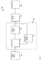
- FIG. 1 is a schematic block diagram of an audio amplifier arrangement 46 which comprises an audio signal source 40, an amplifier unit 45, a low pass filter (LPF) 43 and a loudspeaker 44.
- the amplifier unit 45 comprises a controller 41, a power amplifier 30 and an Analog-to-Digital (AD) converter 42.
- AD Analog-to-Digital
- the input of the amplifier unit 45 receives a digital audio signal from the audio signal source 40.
- the amplifier unit 45 amplifies the audio signal and transmits the amplified signal to the filter 43.
- the filter 43 filters the amplified signal and sends the filtered signal to the loudspeaker 44.
- the audio signal source 40 for example a CD player, mp3 player, radio tuner, etc., provides an audio signal to the amplifier unit 45. This signal typically may have frequency components predominantly in the audible range of about 20 Hz (Hertz) to 22 kHz (kilo Hertz).
- the amplifier unit 45 amplifies the signal and supplies the amplified signal to filter 43 which removes high frequency components from the amplified signal. High frequency is defined as a frequency above the maximum audible frequency of about 22 kHz.
- the filtered signal is then supplied to the loudspeaker 44 which produces sound therefrom.
- the filter 43 is connected upstream to loudspeaker 44.
- the controller 41 receives a digital audio signal from the signal source 40 and a digital signal from the AD converter 42.
- the controller 41 sends a control signal to the amplifier unit 30.
- the amplifier unit 30 outputs an amplified signal to the filter 43.
- the amplified signal from the amplifier unit 30 is also sent to the AD converter 42.
- the controller 41 delivers an essentially distortion free signal to filter 43.
- the controller 41 receives signals from the audio signal source 40 and the AD converter 42. Based at least on these signals, the controller 41 determines the desired output level of the power amplifier unit 30. Then, the controller 41 sets the output of the amplifier unit 30 to the desired level.
- the power amplifier unit 30 is able to provide a positive or negative output voltage. It is also able to source or sink current.
- the amplifier unit 30 uses switching power supply techniques to achieve a high efficiency.
- the AD converter 42 samples the amplified signal from the amplifier unit 30.
- the amplified signal is sampled upstream of the low pass filter 43.
- the AD converter 42 reads the analog voltage value of the sampled signal and transmits the digital voltage value of the sampled signal to the controller 41.
- the AD converter 42 may have high input impedance, which does not alter the sampled signal.
- the AD converter 42 samples the amplified signal at regular time intervals.
- the signal is, e.g., sampled at frequencies of 44 kHz or higher which is the conventional sampling rate of CD audio.
- the maximum frequency of audible signal is about 22 kHz.
- the Nyquist sampling theorem suggests a minimum sampling rate of at least twice this frequency.
- the amplified signal is sampled close to filter 43 in order to sense any distortion in the signal input into filter 43.
- the controller 41 controls the power amplifier unit 30 to compensate for distortions.
- the filter 43 removes unwanted high frequency components in the amplified signal and is located upstream of the loudspeaker 44 to reduce distortions introduced between the filter 43 and the loudspeaker 44.
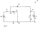
- FIG. 2 is a circuit diagram of an exemplary power amplifier unit 30.
- the amplifier unit 30 is coupled to a load Z and comprises a DC voltage source 13 and a converter circuit 31.
- the converter circuit 31 comprises switches S1 to S6, diodes D1 to D3, an inductor L, a capacitor C, and nodes 34 to 38.
- a first end of switch S1 is coupled to one, e.g. the positive, terminal of the DC voltage source 13 thereby forming node 34.
- the second end of switch S1 is coupled to a first end of switch S2 thereby forming node 35.
- a second end of the switch S2 is coupled to the other, accordingly negative terminal of the voltage source 13 thereby forming node 38.
- a first end of switch S3 is coupled to node 35 and its second end is coupled to the cathode of diode D3.
- a first end of switch S4 is coupled to node 38 and its second end is coupled to the anode of the diode D1 thereby forming node 36.
- a first end of switch S5 is coupled to the cathode of diode D2.
- a second end of the switch S5 is coupled to the anode of the diode D3 thereby forming node 37.
- a first end of the switch S6 is coupled to the positive terminal of voltage source 13 whereas its second end is coupled to the cathode of diode D1.
- the controller 41 of FIG. 1 controls the switches S1 to S6 by means of control signals Q1-Q6.
- the inductor L is connected between node 35 and node 36.
- the anodes of diodes D1 and D2 are coupled to the node 36 whereas the anode of diode D3 is coupled to node 37.
- the cathodes of the diodes D1, D2 and D3 are coupled to the switches S6, S5 and S3, respectively. This provides electrical isolation of the diodes D1, D2 and D3 when the switches S6, S5 and S3 are in an open position.
- the capacitor C is connected between nodes 37 and 38 and load Z is connected between nodes 37 and 38. Node 38 is connected to electrical ground.
- the load Z may have resistive, capacitive, and inductive components.
- the basic energy storage elements of the converter circuit 31 are inductor L and capacitor C.
- the switches S1 to S6 may be of a semiconductor type such as, but not limited to metal-oxide-semiconductor-field-effect transistors (MOSFET) or bipolar transistors.
- MOSFET metal-oxide-semiconductor-field-effect transistors
- NMOSFET n-channel metal-oxide-semiconductor field-effect transistors T1-T6 are used as switches S1-S6.
- the transistors T1 to T6 are of the enhancement type.
- the substrate and the source of each of the transistors T1 to T6 may be connected together to deplete any stray electrons in the substrate.
- the transistors T1 through T6 are of the enhancement type, a high resistance exists between the source and the drain of each transistor.
- An n-channel is formed between the source and the drain of the transistor T1 to T6 when a positive potential difference relative to its source is applied to the gate. This reduces the resistance between its source and its drain.
- a positive potential difference relative to its source is applied to its drain, electrons are caused to flow from its source to its drain.
- electrical current flows from the drain to its source. Accordingly, the drain of the transistor T1 is coupled to the positive terminal of the voltage source 13.
- the substrate of the transistor T1 is connected to its source.
- the source of the transistor T1 is coupled to the drain of the transistor T2 thereby forming node 35.
- the substrate of the transistor T2 is connected to its source.
- the source of the transistor T2 is coupled to the negative terminal of the voltage source 13 thereby forming the node 38.
- the source of the transistor T3 is coupled to node 35 and its drain is coupled to the cathode of diode D3.
- the substrate of transistor T3 is connected to its source.
- the source of transistor T4 is coupled to node 38.
- the substrate of transistor T4 is connected to its source.
- its drain is coupled to the anode of the diode D2 thereby forming node 36.
- the drain of the transistor T5 is coupled to the cathode of the diode D2.
- the substrate of the transistor T5 is connected to its source, which in turn is coupled to the anode of the diode D3 thereby forming node 37.
- the source of the transistor T6 is coupled to the positive terminal of voltage source 13 whereas the drain of the transistor T6 is coupled to the cathode of diode D1.
- the substrate of transistor T6 is connected to its source.
- the gates of transistors T1 to T6 are coupled to the controller 41 of FIG. 1 .
- FIG. 3 is a table of the operating modes of converter circuit 31.
- the converter circuit 31 has four operating modes.
- the positions of switches S1 to S6 determine the operating modes, which establish whether the circuit 31 transfers a positive or negative voltage to load Z and whether the circuit 31 sources or sinks current to load Z.
- the switches S2, S5 and S6 are constantly in an open position and the switches S3 and S4 are constantly in a closed position.
- the circuit 31 transfers a negative voltage from the voltage source 13 to the load Z.
- circuit 31 If circuit 31 operates in mode 2, the switches S3 and S6 are constantly in an open position and the switch S5 is constantly in a closed position. In this mode, the circuit 31 transfers a positive voltage from the DC voltage source 13 to the load Z.
- the circuit 31 In case the circuit 31 operates in mode 3, the switches S1, S2 and S5 are constantly in an open position and the switches S3 and S6 are constantly in a closed position. In this mode, the circuit 31 sinks a current from the load Z that generates a positive voltage.
- the switches S1, S3, and S4 are constantly in an open position and the switches S2 and S6 are constantly in a closed position.
- the circuit 31 sinks current from a load Z that generates a negative voltage.
- FIGS. 4, 5 and 6 show simplified circuit diagrams of the circuit of Fig. 2 for the case that the converter circuit 31 is in operating mode 1.
- the switches S2, S5 and S6 are constantly in an open position if in mode 1.
- the switches S3 and S4 are constantly in a closed position.
- the switch S1 is toggled continuously between the open and a closed position by the controller 41.
- FIG. 4 shows switch S1 in a closed position. This allows the DC voltage V IN of voltage source 13 to be applied to inductor L and the series circuit of diode D3 and load Z.
- the voltage V IN energizes the inductor L and induces a current I L to flow through inductor L.
- the voltage V IN does not induce a flow of current through the series circuit of diode D3 and load Z since diode D3 is blocking the flow of current into the direction from the cathode of the diode D3 to its anode.
- the energy in inductor L keeps the inductor current I L flowing.
- This current I L flows into the load Z and charges the capacitor C.
- the current I L flows from the node 38 to the node 37.
- the voltage V Z generated on the node 37 and the inductor L, with reference to electrical ground, is negative.
- the voltage V Z increases in magnitude as energy from the inductor L is transferred to the capacitor C and the load Z.
- the magnitude of voltage V Z is smaller than the magnitude of the voltage V IN .
- the switch S1 closes. Then, the current I L from the inductor L stops flowing into the load Z. However, current I O from the charged capacitor C flows into the load Z and the voltage V Z decreases as the energy in the capacitor C discharges. Thus, the closing and the opening of switch S1 transfers a negative voltage V Z to the load Z. The voltage V Z rises and falls as the inductor L and the capacitor C are charged and discharged.
- FIGS. 7, 8 , 9, 10 and 11 shows different states of the circuit diagram shown in FIG. 2 in operating mode 2 according to the invention.
- the switches S3 and S6 are constantly in an open position.
- the switch S5 is constantly in a closed position.
- the inactive circuit elements in mode 2 are omitted in the FIG. 7, 8 , 9, 10 and 11 .
- a short circuit replaces the switch S5, in the FIG. 7, 8 , 9, 10 and 11 .
- the converter circuit 31 converts a voltage V IN of the DC voltage source 13 to a positive voltage V Z , which is applied to the load Z.
- Mode 2 has two states of operation. In state 1, the magnitude of voltage V IN is greater than the voltage V Z . In state 2, the magnitude of voltage V IN may be less than the voltage V Z .
- FIGS. 7 and 8 show the circuit 31 in mode 2, state 1.
- the switch S4 is constantly in an open position.
- the switches S1 and S2 are toggled continually between an open and a closed position by a controller, which is not shown in FIGS. 7 and 8 .
- the controller opens the switch S1 when the switch S2 is in the closed position.
- the controller closes the switch S1 when the switch S2 is in the open position.
- the circuit 31 operates in a "buck" converter manner.
- FIG. 7 shows switch S1 in a closed position and switch S2 in an open position.
- This enables the voltage V IN of DC voltage source 13 to be applied across the series circuit of the inductor L, the diode D2 and the load Z.
- This energies the inductor L and causes a current I L to flow through the inductor L and into the load Z.
- the current I L flows from node 37 to node 38.
- the voltage V Z across the load Z starts to increase.
- the voltage V Z of node 37 and of the inductor L, with reference to electrical ground is positive.
- the magnitude of the voltage V IN is greater than the magnitude of the voltage V Z .
- the switch S1 is in an open position and switch S2 is in a closed position.
- the energy in the inductor L keeps the current I L in the inductor L flowing.
- This current I L flows into the load Z.
- This flow depletes the energy in the inductor L thereby reducing the magnitude of the current I L and of the voltage V Z .
- the switches S1 and S2 are toggled continually between an open and a closed position and transfer a positive voltage V Z to the load Z.
- the voltage V Z rises and falls as the energy in the inductor L charges and discharges with the opening and closing of the switches S1 and S2.
- the switch S1 is constantly in a closed position and the switch S2 is constantly in an open position, as shown in FIGS. 9, 10 and 11 .
- Switch S4 is toggled continually between an open and a closed position by a controller, which is not shown.
- the circuit 31 operates in a "boost" converter type manner.
- FIG. 9 shows the switch S4 in a closed position. This enables the voltage V IN of the DC voltage source 13 to be applied across the inductor L. This energies the inductor L and induces a current I L to flow through it.
- Switch S4 is in an open position, as shown in FIG. 10 .
- the current I L continues to flow because of the energised inductor L and the inductor L acts like a voltage source.
- the potential difference across the inductor L and the DC voltage source 13 is applied across the diode D2 and the load Z.
- the voltage V Z across the load Z rises as current starts to flow into the load Z.
- the voltage V Z can rise to a level greater than the voltage V IN due to the additional energy source of the inductor L in series with the voltage source 13.
- the capacitor C is also charged.
- the energy in the inductor L depletes as current I L flows through the inductor L.
- the switch S4 is in a closed position.
- the DC voltage source 13 energises the inductor L.
- a current I O flows from the charged capacitor C into the load Z.
- the voltage V Z falls as the energy in the capacitor C is discharged.
- Switch S4 is toggled continually between an open and a closed position. This transfers a positive voltage V Z to the load Z.
- the magnitude of the voltage V Z may be greater than the magnitude of the voltage V IN .
- the voltage V Z rises and falls as the energy in the inductor L charges and discharges with the opening and closing of the switch S4.
- FIGS. 12 and 13 show the converter circuit 31 of FIG. 2 in operating mode 3.
- the switches S1, S2 and S5 are constantly in an open position in mode 3.
- the switches S3 and S6 are constantly in a closed position.
- Switch S4 is toggled continually between an open and a closed position by the controller 41.
- the inactive circuit elements are omitted in FIGS. 12 and 13 .
- Short circuits replace switches S3 and S6 in FIGS 12 and 13 .
- the converter circuit 31 absorbs energy from the load Z which has a positive voltage.
- the circuit 31 operates in "buck" converter manner where it draws energy from the load Z.
- FIG. 12 shows switch S4 in a closed position.
- the voltage V Z across load Z is applied to the series circuit of diode D3 and inductor L. This induces a current I L to flow through the inductor L from node 37 to node 36. This energises the inductor L and depletes the energy in the load Z.
- the switch S4 is in an open position.
- the current I L continues to flow due to the energized inductor L.
- the inductor L acts like a voltage source.
- the voltage across the load Z and the inductor L is applied to the series circuit of the voltage source 13 and the diodes D1 and D3.
- Current I L depletes the energy in the inductor L.
- the operating mode 3 discharges the energy in the load Z that has a positive voltage.
- FIGS. 14 and 15 show the converter circuit 31 of FIG. 2 in operating mode 4.
- the switches S1, S3, and S4 are constantly in an open position.
- the switches S2 and S6 are constantly in a closed position.
- the switch 5 is toggled continually between an open and a closed position by controller 41.
- the inactive circuit elements are omitted in FIGS. 14 and 15 .
- Short circuits replace the switches S2 and S6 in FIGS. 14 and 15 .
- the converter circuit 31 absorbs energy from the load Z, which has a negative voltage.
- the circuit 31 operates in a "buck-boost" converter type circuit where it reduces the energy stored in load Z.
- the switch 5 is in a closed position, as shown in the FIG. 14 .
- the voltage V Z across the load Z is applied across the series circuit of the diode D2 and the inductor L.
- the load Z has a negative voltage. This induces a current I L to flow in the inductor L from the node 38 to the node 36. This energises the inductor L and depletes the energy in the load Z.
- the switch 5 is in an open position, as shown in FIG. 15 .
- the current I L flows into diode D1 and voltage source 13 such that it reduces the energy in the inductor L and accordingly the voltage across the load Z.
- FIG. 16 shows a line graph 26 of the output voltage of the converter circuit 31 of FIG. 2 whereas the line graph 26 has a sinusoidal waveform.
- the graph 26 starts at 2.5 ms (milliseconds) time point with a value of about 3 volts.
- the graph 26 rises to about 23 volts at the 3.1 ms time point. It then falls to about negative 24 volts at the 4.3 ms time point before rising reaching about negative 15 volts at the 4.6 ms time point.
- the line graph 26 appears as a bold line with a maximum thickness of about 1 volt at the around the 3.1 ms and the 4.3 ms time points.
- the thickness of the graph 26 shows the range of variation of the output of the converter circuit 31.
- the graph 26 comprises a saw-tooth shaped line, which appears as a bold line in the FIG. 16 . Due to its saw-tooth shape, graph 26 fluctuates at high frequencies.
- FIG. 17 shows an expanded view of a portion of the graph 26 of FIG. 16 wherein graph 26 has a saw-tooth waveform of about 300 kilohertz.
- the graph 26 starts at 3.00 ms time point and ends at the 3.03 ms time point.
- the readings of the graph 26 vary between about 21 and 22 volts.
- the graph 26 has a slight upward incline and a peak of about 22.00 volt at the 3.000 ms time point and a peak of about 22.18 volts at the 3.027 ms time point.
- the frequency of the graph 26 corresponds with the toggling frequency of the switches of the circuit 31 of FIG. 2 .
- the output voltage of the converter circuit 31 has a triangle waveform instead of a rectangle form.
- the distortion level introduced by the triangle waveform is at high frequencies.
- the level of distortion is reduced here according to the 1/f 2 rule and not the 1/f rule. Due to this, the disturbance level is very low.
Landscapes
- Engineering & Computer Science (AREA)
- Power Engineering (AREA)
- Dc-Dc Converters (AREA)
- Amplifiers (AREA)
Claims (10)
- Amplificateur en mode commuté (45) comprenant :une unité d'amplificateur commutée (30) qui procure ou absorbe un courant positif ou négatif à ou à partir d'une charge ; ladite charge et ledit courant définissant une tension sur ladite charge ;une unité de commande (41) recevant un signal d'entrée et un signal de réaction et générant des signaux de commande pour l'unité d'amplificateur commutée à partir de ceux-ci ;une unité de réaction (42) connectée à l'unité de commande et à la charge permettant de générer le signal de réaction pour l'unité d'amplificateur commutée à partir de la tension sur la charge ;ladite unité d'amplificateur commutée étant alimentée par une source de tension d'alimentation (13) et comprenant :une bobine d'inductance (L) connectée entre un premier (35) et un deuxième noeud (36) ;ledit premier noeud pouvant être connecté à un troisième noeud (34) au moyen d'un premier commutateur pouvant être commandé (S1), à un quatrième noeud (gnd) au moyen d'un deuxième commutateur pouvant être commandé (S2), et à un cinquième noeud (37) au moyen d'un troisième commutateur pouvant être commandé (S3) et d'une première unité de diode (D3) ;ledit deuxième noeud pouvant être connecté au quatrième noeud au moyen d'un quatrième commutateur pouvant être commandé (S4) et au cinquième noeud au moyen d'un cinquième commutateur pouvant être commandé (S5) et d'une deuxième diode (D2) ;lesdits premier et deuxième noeuds peuvent être connectés au moyen d'un sixième commutateur pouvant être commandé (S6) et d'une troisième diode (D1) ;les commutateurs étant connectés à et commandés par l'unité de commande, ladite source de tension d'alimentation étant connectée entre le troisième noeud et le quatrième noeud et ladite charge étant connectée entre le cinquième noeud et le quatrième noeud.
- L'amplificateur de la revendication 1, dans lequel les commutateurs dans l'unité d'amplificateur sont commandés par l'unité de commande au moyen de laquelle, en fonction du signal d'entrée, l'unité d'amplificateur est commandée comme un convertisseur abaisseur de tension non inverseur, un convertisseur élévateur de tension non inverseur, un convertisseur abaisseur de tension inverseur ou un convertisseur élévateur de tension inverseur.
- L'amplificateur d'une des revendications 1 ou 2 comprenant en outre un condensateur connecté entre le cinquième noeud et le quatrième noeud.
- L'amplificateur d'une des revendications 1, 2 ou 3 comprenant en outre une unité de filtre connectée en amont de la charge.
- L'amplificateur de la revendication 4, dans lequel le filtre est un filtre passe-bas.
- L'amplificateur de l'une des revendications 1 à 5, dans lequel l'unité de réaction comprend un convertisseur analogique-numérique.
- L'amplificateur de l'une des revendications 1 à 6, dans lequel les commutateurs pouvant être commandés sont des dispositifs semiconducteurs.
- L'amplificateur de la revendication 7, dans lequel les commutateurs pouvant être commandés sont des MOSFET.
- L'amplificateur de la revendication 8, dans lequel les commutateurs pouvant être commandés sont des MOSFET de type à enrichissement.
- L'amplificateur de l'une des revendications 1 à 6, dans lequel l'unité de commande effectue un traitement de signaux numériques.
Priority Applications (4)
| Application Number | Priority Date | Filing Date | Title |
|---|---|---|---|
| AT08003732T ATE518299T1 (de) | 2008-02-28 | 2008-02-28 | Getakteter verstärker |
| EP08003732A EP2096752B1 (fr) | 2008-02-28 | 2008-02-28 | Amplificateur de mode commuté |
| PCT/EP2009/001116 WO2009106249A1 (fr) | 2008-02-28 | 2009-02-18 | Amplificateur en mode commuté |
| US12/920,017 US8143945B2 (en) | 2008-02-28 | 2009-02-18 | Switched mode amplifier |
Applications Claiming Priority (1)
| Application Number | Priority Date | Filing Date | Title |
|---|---|---|---|
| EP08003732A EP2096752B1 (fr) | 2008-02-28 | 2008-02-28 | Amplificateur de mode commuté |
Publications (2)
| Publication Number | Publication Date |
|---|---|
| EP2096752A1 EP2096752A1 (fr) | 2009-09-02 |
| EP2096752B1 true EP2096752B1 (fr) | 2011-07-27 |
Family
ID=39356206
Family Applications (1)
| Application Number | Title | Priority Date | Filing Date |
|---|---|---|---|
| EP08003732A Active EP2096752B1 (fr) | 2008-02-28 | 2008-02-28 | Amplificateur de mode commuté |
Country Status (4)
| Country | Link |
|---|---|
| US (1) | US8143945B2 (fr) |
| EP (1) | EP2096752B1 (fr) |
| AT (1) | ATE518299T1 (fr) |
| WO (1) | WO2009106249A1 (fr) |
Families Citing this family (7)
| Publication number | Priority date | Publication date | Assignee | Title |
|---|---|---|---|---|
| US8773196B2 (en) * | 2011-09-30 | 2014-07-08 | Clevech Corporation | Resource pooling amplifier |
| WO2014110474A1 (fr) * | 2013-01-14 | 2014-07-17 | Cognipower, Llc | Amplificateur à transfert indirect avec rétroaction directe |
| EP2768136A1 (fr) * | 2013-02-13 | 2014-08-20 | ST-Ericsson SA | Amplificateur audio |
| US9825616B2 (en) * | 2013-03-15 | 2017-11-21 | Avago Technologies General Ip (Singapore) Pte. Ltd. | Circuit for reducing slope magnitude during increasing and decreasing voltage transitions |
| WO2015119956A2 (fr) * | 2014-02-04 | 2015-08-13 | Cirrus Logic, Inc. | Amplificateur en mode commuté |
| WO2015171940A1 (fr) | 2014-05-08 | 2015-11-12 | Cirrus Logic, Inc. | Convertisseur à découpage avec mode linéaire basse tension |
| US9628033B2 (en) | 2014-10-29 | 2017-04-18 | Cirrus Logic, Inc. | Power stage with switched mode amplifier and linear amplifier |
Family Cites Families (5)
| Publication number | Priority date | Publication date | Assignee | Title |
|---|---|---|---|---|
| WO1994011799A1 (fr) * | 1992-11-10 | 1994-05-26 | Motorola, Inc. | Regulateur de commutation et systeme amplificateur |
| US5610553A (en) | 1993-03-02 | 1997-03-11 | Kirn; Larry | Switching amplifier with impedance transformation output stage |
| US6304137B1 (en) * | 1999-12-23 | 2001-10-16 | Red Chip Company Limited | Output stage for high power class D amplifiers |
| DE10126236B4 (de) | 2001-05-30 | 2008-04-17 | Harman Becker Automotive Systems Gmbh | Verstärker |
| US7307474B2 (en) * | 2004-12-21 | 2007-12-11 | Nphysics, Inc. | Integrated booster amplifier |
-
2008
- 2008-02-28 AT AT08003732T patent/ATE518299T1/de not_active IP Right Cessation
- 2008-02-28 EP EP08003732A patent/EP2096752B1/fr active Active
-
2009
- 2009-02-18 WO PCT/EP2009/001116 patent/WO2009106249A1/fr active Application Filing
- 2009-02-18 US US12/920,017 patent/US8143945B2/en active Active
Also Published As
| Publication number | Publication date |
|---|---|
| EP2096752A1 (fr) | 2009-09-02 |
| US20110032034A1 (en) | 2011-02-10 |
| WO2009106249A1 (fr) | 2009-09-03 |
| ATE518299T1 (de) | 2011-08-15 |
| US8143945B2 (en) | 2012-03-27 |
Similar Documents
| Publication | Publication Date | Title |
|---|---|---|
| EP2096752B1 (fr) | Amplificateur de mode commuté | |
| US8416017B2 (en) | Circuit and method for reducing noise in class D amplifiers | |
| TWI475349B (zh) | 電壓調節器、包絡追蹤電源系統、傳輸模組、及集成電路設備 | |
| CN107070423B (zh) | 用于实现d类放大器的高输出信号摆幅的方法及设备 | |
| USRE42846E1 (en) | Close-loop class-D audio amplifier and control method thereof | |
| KR101704609B1 (ko) | 플로팅 레일들을 갖는 스위칭 전력 스테이지들을 포함하는 차지-리사이클링 회로들 | |
| US7906945B2 (en) | Soft-start voltage circuit | |
| KR20200091398A (ko) | 복수의 독립된 출력 스테이지들을 가진 클래스-d 증폭기 | |
| Sepahvand et al. | Monolithic multilevel GaN converter for envelope tracking in RF power amplifiers | |
| Trescases et al. | Predictive efficiency optimization for DC–DC converters with highly dynamic digital loads | |
| CN211405976U (zh) | 音频放大器和集成电路 | |
| CN108432112A (zh) | Dc-dc变换器以及负载驱动用半导体集成电路 | |
| JP5725026B2 (ja) | 電源変調器及びその制御方法 | |
| US7812583B2 (en) | Management of regulator-induced switching noise for sampled systems | |
| JP6679750B2 (ja) | 電気負荷を駆動するための回路および方法 | |
| Li et al. | High efficiency wide bandwidth power supplies for GSM and EDGE RF power amplifiers | |
| EP3834284A1 (fr) | Appareil et procédé d'aide au suivi d'enveloppe avec réponse transitoire dans une tension d'alimentation pour amplificateur de puissance | |
| US20230098806A1 (en) | Switching amplifier having linear transition totem pole modulation | |
| JP6186135B2 (ja) | D級アンプおよび電子機器 | |
| US11005427B2 (en) | Audible noise reduction in an audio power amplifier | |
| US20240283351A1 (en) | Detecting signals from cascode power devices | |
| US20240094265A1 (en) | Current sensing systems and associated methods | |
| CN115580114A (zh) | 开关电源 | |
| CN114793095A (zh) | 单级升压d类放大器 | |
| CN118523586A (zh) | 检测来自共源共栅功率器件的信号 |
Legal Events
| Date | Code | Title | Description |
|---|---|---|---|
| PUAI | Public reference made under article 153(3) epc to a published international application that has entered the european phase |
Free format text: ORIGINAL CODE: 0009012 |
|
| AK | Designated contracting states |
Kind code of ref document: A1 Designated state(s): AT BE BG CH CY CZ DE DK EE ES FI FR GB GR HR HU IE IS IT LI LT LU LV MC MT NL NO PL PT RO SE SI SK TR |
|
| AX | Request for extension of the european patent |
Extension state: AL BA MK RS |
|
| 17P | Request for examination filed |
Effective date: 20100225 |
|
| 17Q | First examination report despatched |
Effective date: 20100323 |
|
| AKX | Designation fees paid |
Designated state(s): AT BE BG CH CY CZ DE DK EE ES FI FR GB GR HR HU IE IS IT LI LT LU LV MC MT NL NO PL PT RO SE SI SK TR |
|
| GRAP | Despatch of communication of intention to grant a patent |
Free format text: ORIGINAL CODE: EPIDOSNIGR1 |
|
| GRAS | Grant fee paid |
Free format text: ORIGINAL CODE: EPIDOSNIGR3 |
|
| GRAA | (expected) grant |
Free format text: ORIGINAL CODE: 0009210 |
|
| AK | Designated contracting states |
Kind code of ref document: B1 Designated state(s): AT BE BG CH CY CZ DE DK EE ES FI FR GB GR HR HU IE IS IT LI LT LU LV MC MT NL NO PL PT RO SE SI SK TR |
|
| REG | Reference to a national code |
Ref country code: GB Ref legal event code: FG4D |
|
| REG | Reference to a national code |
Ref country code: CH Ref legal event code: EP |
|
| REG | Reference to a national code |
Ref country code: DE Ref legal event code: R096 Ref document number: 602008008456 Country of ref document: DE Effective date: 20110915 |
|
| REG | Reference to a national code |
Ref country code: NL Ref legal event code: VDEP Effective date: 20110727 |
|
| REG | Reference to a national code |
Ref country code: AT Ref legal event code: MK05 Ref document number: 518299 Country of ref document: AT Kind code of ref document: T Effective date: 20110727 |
|
| PG25 | Lapsed in a contracting state [announced via postgrant information from national office to epo] |
Ref country code: IS Free format text: LAPSE BECAUSE OF FAILURE TO SUBMIT A TRANSLATION OF THE DESCRIPTION OR TO PAY THE FEE WITHIN THE PRESCRIBED TIME-LIMIT Effective date: 20111127 Ref country code: SE Free format text: LAPSE BECAUSE OF FAILURE TO SUBMIT A TRANSLATION OF THE DESCRIPTION OR TO PAY THE FEE WITHIN THE PRESCRIBED TIME-LIMIT Effective date: 20110727 Ref country code: BE Free format text: LAPSE BECAUSE OF FAILURE TO SUBMIT A TRANSLATION OF THE DESCRIPTION OR TO PAY THE FEE WITHIN THE PRESCRIBED TIME-LIMIT Effective date: 20110727 Ref country code: PT Free format text: LAPSE BECAUSE OF FAILURE TO SUBMIT A TRANSLATION OF THE DESCRIPTION OR TO PAY THE FEE WITHIN THE PRESCRIBED TIME-LIMIT Effective date: 20111128 Ref country code: NL Free format text: LAPSE BECAUSE OF FAILURE TO SUBMIT A TRANSLATION OF THE DESCRIPTION OR TO PAY THE FEE WITHIN THE PRESCRIBED TIME-LIMIT Effective date: 20110727 Ref country code: HR Free format text: LAPSE BECAUSE OF FAILURE TO SUBMIT A TRANSLATION OF THE DESCRIPTION OR TO PAY THE FEE WITHIN THE PRESCRIBED TIME-LIMIT Effective date: 20110727 Ref country code: NO Free format text: LAPSE BECAUSE OF FAILURE TO SUBMIT A TRANSLATION OF THE DESCRIPTION OR TO PAY THE FEE WITHIN THE PRESCRIBED TIME-LIMIT Effective date: 20111027 Ref country code: LT Free format text: LAPSE BECAUSE OF FAILURE TO SUBMIT A TRANSLATION OF THE DESCRIPTION OR TO PAY THE FEE WITHIN THE PRESCRIBED TIME-LIMIT Effective date: 20110727 Ref country code: FI Free format text: LAPSE BECAUSE OF FAILURE TO SUBMIT A TRANSLATION OF THE DESCRIPTION OR TO PAY THE FEE WITHIN THE PRESCRIBED TIME-LIMIT Effective date: 20110727 |
|
| PG25 | Lapsed in a contracting state [announced via postgrant information from national office to epo] |
Ref country code: GR Free format text: LAPSE BECAUSE OF FAILURE TO SUBMIT A TRANSLATION OF THE DESCRIPTION OR TO PAY THE FEE WITHIN THE PRESCRIBED TIME-LIMIT Effective date: 20111028 Ref country code: CY Free format text: LAPSE BECAUSE OF FAILURE TO SUBMIT A TRANSLATION OF THE DESCRIPTION OR TO PAY THE FEE WITHIN THE PRESCRIBED TIME-LIMIT Effective date: 20110727 Ref country code: AT Free format text: LAPSE BECAUSE OF FAILURE TO SUBMIT A TRANSLATION OF THE DESCRIPTION OR TO PAY THE FEE WITHIN THE PRESCRIBED TIME-LIMIT Effective date: 20110727 Ref country code: PL Free format text: LAPSE BECAUSE OF FAILURE TO SUBMIT A TRANSLATION OF THE DESCRIPTION OR TO PAY THE FEE WITHIN THE PRESCRIBED TIME-LIMIT Effective date: 20110727 Ref country code: SI Free format text: LAPSE BECAUSE OF FAILURE TO SUBMIT A TRANSLATION OF THE DESCRIPTION OR TO PAY THE FEE WITHIN THE PRESCRIBED TIME-LIMIT Effective date: 20110727 Ref country code: LV Free format text: LAPSE BECAUSE OF FAILURE TO SUBMIT A TRANSLATION OF THE DESCRIPTION OR TO PAY THE FEE WITHIN THE PRESCRIBED TIME-LIMIT Effective date: 20110727 |
|
| PG25 | Lapsed in a contracting state [announced via postgrant information from national office to epo] |
Ref country code: CZ Free format text: LAPSE BECAUSE OF FAILURE TO SUBMIT A TRANSLATION OF THE DESCRIPTION OR TO PAY THE FEE WITHIN THE PRESCRIBED TIME-LIMIT Effective date: 20110727 Ref country code: SK Free format text: LAPSE BECAUSE OF FAILURE TO SUBMIT A TRANSLATION OF THE DESCRIPTION OR TO PAY THE FEE WITHIN THE PRESCRIBED TIME-LIMIT Effective date: 20110727 |
|
| PG25 | Lapsed in a contracting state [announced via postgrant information from national office to epo] |
Ref country code: RO Free format text: LAPSE BECAUSE OF FAILURE TO SUBMIT A TRANSLATION OF THE DESCRIPTION OR TO PAY THE FEE WITHIN THE PRESCRIBED TIME-LIMIT Effective date: 20110727 Ref country code: IT Free format text: LAPSE BECAUSE OF FAILURE TO SUBMIT A TRANSLATION OF THE DESCRIPTION OR TO PAY THE FEE WITHIN THE PRESCRIBED TIME-LIMIT Effective date: 20110727 Ref country code: EE Free format text: LAPSE BECAUSE OF FAILURE TO SUBMIT A TRANSLATION OF THE DESCRIPTION OR TO PAY THE FEE WITHIN THE PRESCRIBED TIME-LIMIT Effective date: 20110727 |
|
| PLBE | No opposition filed within time limit |
Free format text: ORIGINAL CODE: 0009261 |
|
| STAA | Information on the status of an ep patent application or granted ep patent |
Free format text: STATUS: NO OPPOSITION FILED WITHIN TIME LIMIT |
|
| PG25 | Lapsed in a contracting state [announced via postgrant information from national office to epo] |
Ref country code: DK Free format text: LAPSE BECAUSE OF FAILURE TO SUBMIT A TRANSLATION OF THE DESCRIPTION OR TO PAY THE FEE WITHIN THE PRESCRIBED TIME-LIMIT Effective date: 20110727 |
|
| 26N | No opposition filed |
Effective date: 20120502 |
|
| REG | Reference to a national code |
Ref country code: DE Ref legal event code: R097 Ref document number: 602008008456 Country of ref document: DE Effective date: 20120502 |
|
| PG25 | Lapsed in a contracting state [announced via postgrant information from national office to epo] |
Ref country code: MC Free format text: LAPSE BECAUSE OF NON-PAYMENT OF DUE FEES Effective date: 20120229 |
|
| REG | Reference to a national code |
Ref country code: CH Ref legal event code: PL |
|
| PG25 | Lapsed in a contracting state [announced via postgrant information from national office to epo] |
Ref country code: CH Free format text: LAPSE BECAUSE OF NON-PAYMENT OF DUE FEES Effective date: 20120229 Ref country code: LI Free format text: LAPSE BECAUSE OF NON-PAYMENT OF DUE FEES Effective date: 20120229 |
|
| REG | Reference to a national code |
Ref country code: IE Ref legal event code: MM4A |
|
| PG25 | Lapsed in a contracting state [announced via postgrant information from national office to epo] |
Ref country code: IE Free format text: LAPSE BECAUSE OF NON-PAYMENT OF DUE FEES Effective date: 20120228 |
|
| PG25 | Lapsed in a contracting state [announced via postgrant information from national office to epo] |
Ref country code: ES Free format text: LAPSE BECAUSE OF FAILURE TO SUBMIT A TRANSLATION OF THE DESCRIPTION OR TO PAY THE FEE WITHIN THE PRESCRIBED TIME-LIMIT Effective date: 20111107 |
|
| PG25 | Lapsed in a contracting state [announced via postgrant information from national office to epo] |
Ref country code: BG Free format text: LAPSE BECAUSE OF FAILURE TO SUBMIT A TRANSLATION OF THE DESCRIPTION OR TO PAY THE FEE WITHIN THE PRESCRIBED TIME-LIMIT Effective date: 20111027 |
|
| PG25 | Lapsed in a contracting state [announced via postgrant information from national office to epo] |
Ref country code: MT Free format text: LAPSE BECAUSE OF FAILURE TO SUBMIT A TRANSLATION OF THE DESCRIPTION OR TO PAY THE FEE WITHIN THE PRESCRIBED TIME-LIMIT Effective date: 20110727 |
|
| PG25 | Lapsed in a contracting state [announced via postgrant information from national office to epo] |
Ref country code: TR Free format text: LAPSE BECAUSE OF FAILURE TO SUBMIT A TRANSLATION OF THE DESCRIPTION OR TO PAY THE FEE WITHIN THE PRESCRIBED TIME-LIMIT Effective date: 20110727 |
|
| PG25 | Lapsed in a contracting state [announced via postgrant information from national office to epo] |
Ref country code: LU Free format text: LAPSE BECAUSE OF NON-PAYMENT OF DUE FEES Effective date: 20120228 |
|
| PG25 | Lapsed in a contracting state [announced via postgrant information from national office to epo] |
Ref country code: HU Free format text: LAPSE BECAUSE OF FAILURE TO SUBMIT A TRANSLATION OF THE DESCRIPTION OR TO PAY THE FEE WITHIN THE PRESCRIBED TIME-LIMIT Effective date: 20080228 |
|
| REG | Reference to a national code |
Ref country code: FR Ref legal event code: PLFP Year of fee payment: 8 |
|
| PGFP | Annual fee paid to national office [announced via postgrant information from national office to epo] |
Ref country code: FR Payment date: 20150217 Year of fee payment: 8 |
|
| REG | Reference to a national code |
Ref country code: FR Ref legal event code: ST Effective date: 20161028 |
|
| PG25 | Lapsed in a contracting state [announced via postgrant information from national office to epo] |
Ref country code: FR Free format text: LAPSE BECAUSE OF NON-PAYMENT OF DUE FEES Effective date: 20160229 |
|
| P01 | Opt-out of the competence of the unified patent court (upc) registered |
Effective date: 20230526 |
|
| PGFP | Annual fee paid to national office [announced via postgrant information from national office to epo] |
Ref country code: DE Payment date: 20240123 Year of fee payment: 17 Ref country code: GB Payment date: 20240123 Year of fee payment: 17 |