EP2093827A1 - Non-reciprocal circuit device - Google Patents
Non-reciprocal circuit device Download PDFInfo
- Publication number
- EP2093827A1 EP2093827A1 EP09002236A EP09002236A EP2093827A1 EP 2093827 A1 EP2093827 A1 EP 2093827A1 EP 09002236 A EP09002236 A EP 09002236A EP 09002236 A EP09002236 A EP 09002236A EP 2093827 A1 EP2093827 A1 EP 2093827A1
- Authority
- EP
- European Patent Office
- Prior art keywords
- matching
- center conductors
- circuit device
- capacitor
- reciprocal circuit
- Prior art date
- Legal status (The legal status is an assumption and is not a legal conclusion. Google has not performed a legal analysis and makes no representation as to the accuracy of the status listed.)
- Granted
Links
Images


Classifications
-
- H—ELECTRICITY
- H01—ELECTRIC ELEMENTS
- H01P—WAVEGUIDES; RESONATORS, LINES, OR OTHER DEVICES OF THE WAVEGUIDE TYPE
- H01P1/00—Auxiliary devices
- H01P1/32—Non-reciprocal transmission devices
-
- H—ELECTRICITY
- H01—ELECTRIC ELEMENTS
- H01P—WAVEGUIDES; RESONATORS, LINES, OR OTHER DEVICES OF THE WAVEGUIDE TYPE
- H01P1/00—Auxiliary devices
- H01P1/32—Non-reciprocal transmission devices
- H01P1/38—Circulators
- H01P1/383—Junction circulators, e.g. Y-circulators
-
- H—ELECTRICITY
- H01—ELECTRIC ELEMENTS
- H01P—WAVEGUIDES; RESONATORS, LINES, OR OTHER DEVICES OF THE WAVEGUIDE TYPE
- H01P1/00—Auxiliary devices
- H01P1/32—Non-reciprocal transmission devices
- H01P1/36—Isolators
Definitions
- the present invention relates to a circuit element including a magnetic plate, more particularly to a non-reciprocal circuit device.
- a lumped constant non-reciprocal circuit device has long been used as an isolator or circulator in a mobile communication device or mobile communication terminal because it requires less space.
- An isolator is placed between the power amplifier and antenna in the transmitter of a mobile communication device in order to, for example, prevent unwanted signals from reversely entering the power amplifier from the antenna for a desired frequency band or to stabilize impedance on the load side of the power amplifier; a circulator is used in a transmission/reception branch circuit etc.
- Fig. 15 is a transparent perspective view illustrating the internal structure of a conventional lumped constant circulator (referred to below simply as circulator 100).
- Fig. 16 is a circuit diagram illustrating the equivalent circuit of the circulator in Fig. 15 . In the equivalent circuit in Fig. 16 , a ferrite plate F1 is not shown.
- ferrite plate F1 and F2 are placed between a ferrite plate F1 and a ferrite plate F2 (not shown) of the same shape as ferrite plate F1, and permanent magnets (not shown) for magnetizing ferrite plates F1 and F2 are disposed facing each other so as to sandwich ferrite plate F1 and F2 therebetween.
- center conductors L1, L2, and L3 projects externally from the rims of ferrite plates F1 and F2 and the projection is connected to a signal input/output port (not shown) and one end of each of matching dielectric board pieces (matching capacitors) C1, C2, and C3.
- the other end of each of center conductors L1, L2, and L3 and the other end of each of matching dielectric board pieces (matching capacitors) C1, C2, and C3 are grounded electrically.
- Center conductors L1, L2, and L3 have inductance. When a lumped constant circuit element is used as an isolator, the input/output port of center conductor L3 is connected to one end of a terminator and the other end is grounded electrically to absorb reflected signals.
- circulator 100 shows irreversibility in a certain frequency range. That is, circulator 100 has high attenuation characteristics (isolation) for a signal that is input to the input/output port connected to one end of the center conductor L1 and output from the input/output port connected to one end of the center conductor L2, a signal that is input to the input/output port connected to one end of the center conductor L2 and output from the input/output port connected to one end of the center conductor L3, and a signal that is input to the input/output port connected to one end of the center conductor L3 and output from the input/output port connected to one end of center conductor L1; circulator 100 has low attenuation characteristics (or opposite characteristics) for signals that are transmitted in the directions opposite to those.
- the non-reciprocal circuit device functions as an isolator, in the corresponding frequency band, which has high attenuation characteristics for a signal that is input to the input/output port connected to one end of the center conductor L1 and output from the input/output port connected to one end of center conductor L2 and has low attenuation characteristics (or opposite characteristics) for signals that are transmitted in the direction opposite to that.
- the frequency (operating frequency) bandwidth in which a non-reciprocal circuit device such as a conventional isolator or circulator shows irreversibility is generally narrow.
- the frequency bandwidth that gives attenuation with an irreversibility of 20 dB at a center frequency of 2 GHz is several tens of hertz.
- Non-patent literature 1 discloses technology for widening the bandwidth of the operating frequency of an isolator. This known technology achieves a bandwidth ratio of 7.7 % at a center frequency of 924 MHz by adding an inductor or capacitor to the input end of an isolator.
- Non-patent literature 2 discloses an example of increasing the fractional bandwidth to 30 to 60 % by adding an inductor or capacitor between a center conductor and the ground.
- Patent literature 1 discloses technology for widening the bandwidth without increasing insertion loss by providing a capacitor between a ground conductor connected to one end of each of three center conductors and the ground.
- Patent literature 2 discloses a non-reciprocal circuit device that changes the operating frequency with an RF switch for disconnecting or connecting a capacitor disposed on the input/output port of each center conductor to change the resonance frequency of a resonant circuit. In this structure, however, the operating frequency is toggled with the switch, so concurrent use in a plurality of frequency bands is impossible, thereby disabling its usage in an environment in which a plurality of applications for different frequency bands are implemented concurrently.
- Patent literature 3 discloses a non-reciprocal circuit device that changes operating frequency bands by changing the reactance of a variable capacitor disposed on mutual connection ends of the three center conductors. Since reactance needs to be changed in this structure, however, it is not applicable to an environment in which a plurality of applications for different frequency bands are implemented concurrently as in the structure in patent literature 2.
- Patent literature 4 discloses a structure in which two isolators are placed in series with two ferrite plates for dual-band support using an installation area of the size equivalent to that for a single band isolator.
- application to portable terminals is difficult because the height is increased in this structure.
- the present invention addresses the above problems with the object of providing a dual-band-capable non-reciprocal circuit device that can solely obtain irreversibility concurrently in two frequency bands significantly apart even though the circuit element has a size equivalent to that of a single-band-capable lumped constant non-reciprocal circuit device in order to achieve multiband/multimode terminals.
- a non-reciprocal circuit device of the present invention comprises a magnetic plate; a plurality of center conductors, each of which has a first end and a second end, the plurality of center conductors being mutually insulated and disposed so as to intersect on the magnetic plate; a plane conductor disposed facing the plurality of center conductors with the magnetic plate placed between the plane conductor and the plurality of center conductors, the plane conductor being connected to the first ends of all of the plurality of center conductors; a plurality of matching capacitors, each of which has a first end and a second end, the first end being grounded electrically, the second end being connected to the second end of corresponding one of the plurality of center conductors; a plurality of first matching circuits, each of which has a first and a second end, the first end being connected to the second end of corresponding one of the plurality of center conductors, the second end being an input/output port; and a second matching circuit having a first end and a second end, the
- the non-reciprocal circuit device of the present invention can solely obtain irreversibility concurrently in two frequency bands significantly apart even though the circuit element has a size equivalent to that of a single-band-capable lumped constant non-reciprocal circuit device.
- Fig. 1 is a transparent perspective view illustrating an example of the structure of a non-reciprocal circuit device 10 in a first embodiment.
- Fig. 2 is an exploded perspective view of the non-reciprocal circuit device 10 in Fig. 1 .
- non-reciprocal circuit device 10 includes center conductors L1, L2, and L3, matching dielectric board pieces C1, C2, and C3, a ferrite plate (i.e., magnetic plate) F1, a plane conductor P1, first matching circuits M11, M12, and M13, and a second matching circuit M2 (dielectric plate D1 in Fig. 1 ).
- the first matching circuit M11 includes a pair of inductor L11 and capacitor C11
- the first matching circuit M12 includes a pair of inductor L12 and capacitor C12
- the first matching circuit M 13 includes a pair of inductor L 13 and capacitor C 13.
- the plane conductor P1 is a disc-shaped conductor integrated with the center conductors L1, L2, and L3; the first ends of the center conductors L1, L2, and L3 are connected to the three points dividing the rim of the plane conductor P1 into three equal parts. The first ends of the center conductors L1, L2, and L3 are mutually short-circuited and each of the second ends has two parallel lines connected to the rim of the plane conductor P1.
- the disc-shaped ferrite plate F1 is placed on one surface (top surface in Fig. 1 ) of the plane conductor P1.
- the three center conductors L1, L2, and L3 are superimposed on the top surface of the ferrite plate F1 (top surface in Fig.
- the center conductors L1, L2, and L3 are mutually insulated at the intersections. It is not necessary to make the center conductors intersect at the same angle and to place the center conductors so that their barycenters match as in this example. Preferably, the center conductors intersect at the same angle and their barycenters match in order to obtain sufficient irreversibility or make adjustment of frequency easier.
- a capacitor C31 with a desired capacity is formed by loading dielectric plate D1 between the plane conductor P1 and the ground conductor G as shown in Fig. 3A and the capacitor C31 functions as the second matching circuit M2.
- This capacitor C31 can be a parallel plate capacitor formed between a conductive layer 21 formed on the ground side of the dielectric plate D1 opposite from the plane conductor P1, and the plane conductor P1, as shown in Fig. 3B .
- This capacitor C31 can also be a chip capacitor connected between the plane conductor P1 and the ground conductor G instead of using a dielectric plate D1, as shown in Fig. 3C .
- a capacitor dielectric plate D1 in Fig. 2
- Projection ends S1, S2, and S3 (opposite to the ends connected to the plane conductor P1) of the center conductors L1, L2, and L3 project externally from the rim of the ferrite plate F1.
- the projection ends S1, S2, and S3 are connected to the first ends of the inductors L11, L12, and L 13, respectively.
- Matching dielectric board pieces C1, C2, and C3 are further attached on the surfaces of the projection ends S1, S2, and S3, which face the ground conductor, to form matching capacitors between each of the projection ends S1, S2, and S3 and the ground conductor G.
- Reference characters C1, C2, and C3 for matching dielectric board pieces are also used below as the reference characters of these matching capacitors.
- the second ends of the inductors L11, L12, and L13 configure input/output ports SS1, SS2, and SS3, respectively, and are connected to the first ends of the capacitors C11, C12, and C13, respectively.
- the second ends of the capacitors C11, C12, and C 13 are grounded electrically. Pairs of an inductor and a capacitor, (L11, C 11), (L12, C12), and (L 13, C13), constitute the first matching circuits M11, M12, and M13, respectively.
- a chip inductor, a line with a certain length, etc. can be used to implement each of the inductors L11 to L13.
- a chip capacitor, a varactor such as a PIN diode, etc. can be used or a dielectric having one end grounded can be sandwiched to implement each of the capacitors C 11 to C 13.
- a permanent magnet for magnetizing the ferrite plate F1 is actually disposed facing the ferrite plate F1, but the permanent magnet is not shown in the figure.
- Fig. 4 is a block diagram of the structure of the present invention.
- Fig. 5 shows a configuration obtainable by adding an example of the equivalent circuit of a circulator unit 10A to Fig. 4 (ferrite plate F1 is not shown).
- An equivalent circuit of the conventional circulator corresponds to the equivalent circuit of the circulator unit 10A in Fig. 5 in which P1 is grounded.
- the circuit configuration of non-reciprocal circuit device 10 will be described below with reference to Fig. 5 .
- the ends of the three center conductors L1, L2, and L3, that are opposite to the projection ends S1, S2, and S3 are mutually connected and the connection ends S4 are connected to the plane conductor P1.
- the first ends of the center conductor L1, L2, and L3 are connected mutually because they are connected to the plane conductor P1.
- a first end of the second matching circuit M2 is connected to the plane conductor P1 and a second end is grounded electrically.
- the second matching circuit M2 is configured as, for example, a capacitor C31 as shown in Fig. 7A , more specifically can be achieved by loading a dielectric plate D1 between the plane conductor P1 and the ground conductor G as shown in Figs.
- the first matching circuit M11 has a pair of, for example, inductor L11 and capacitor C11 as shown in Fig. 6A . More specifically, the inductor L 11 is connected between the center conductor L1 and the input/output port SS1 and one end of the capacitor C11 is connected to either end of the inductor L 11 and the other end is grounded.
- the first matching circuits M12 and M 13 also comprise a pair of inductor L12 and capacitor C12 and a pair of inductor L13 and capacitor C 13, respectively.
- the first frequency band (higher frequency side) of the dual-band is determined mainly by the center conductors L1, L2, and L3, the matching capacitors C1, C2, and C3, and the inductances and capacitances of the first matching circuits M11, M12, and M13.
- the second frequency band (lower frequency side) of the dual-band is determined mainly by the inductances and capacitances of the first matching circuits M11, M12, and M13 and the inductance and capacitance of the second matching circuit M2. If the capacitances of the matching capacitors C1, C2, and C3 are increased, the interval between the two frequency bands (first frequency band and second frequency band) is reduced.
- the first matching circuits M11, M12, and M13 and the second matching circuit M2 If fine tuning is performed by the first matching circuits M11, M12, and M13 and the second matching circuit M2, high isolation can be achieved with low transmission loss.
- the capacitances of the first matching circuits M11, M12, and M13 are increased and the inductances are reduced, the operating frequency bands can be shifted to the lower side; if the capacitances are reduced and the inductances are increased, the operating frequency bands can be shifted to the higher side.
- the insertion loss and degradation in isolation characteristics depend on the characteristics (such as the size and saturation magnetization) of the ferrite plate F1 or the external magnetic field strength.
- the lower limit of the second operating frequency band shifted by adjustment of the inductance or capacitance depends on these characteristics.
- the second operating frequency band can be shifted to a lower side.
- a shift to a lower side is achieved by, for example, increasing the diameter of the ferrite plate, selecting a ferrite with a lower saturation magnetization, or reducing the external magnetization strength.
- reference characters L1, L2, and L3 for the center conductors also indicate their line lengths
- reference characters L 11, L 12, and L 13 for the inductors also indicate their inductances
- reference characters C1, C2, and C3 for the capacitors also indicate their capacitances.
- Fig. 8 is a graph showing transmission characteristics S12 and S21 of the circulator indicated by the equivalent circuit in Fig. 5 in the first embodiment.
- the first matching circuits M11, M12, and M 13 have the structure shown in Fig. 6A and the second matching circuit M2 has the structure shown in Fig. 7A .
- the values of L1 to L3 are 2.9 mm
- the values of C1 to C3 are 2.1 to 2.2 pF
- the values of L11 to L 13 are 1.9 to 2.0 nH
- the values of C11 to C 13 are 2.3 to 2.5 pF
- the value of C31 is 0.33 pF.
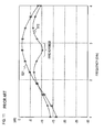
- the frequency bands in which an irreversibility of 20 dB or more can be obtained are the 1.6 GHz and 3.7 GHz bands, and irreversibility can be achieved in both of the frequency bands more than one octave band apart.
- 100 MHz or more of bandwidth with an isolation of 20 dB or more can be obtained in both of the frequency bands.
- Fig. 9 is a graph showing transmission characteristics S12 and S21 of the circulator from which the second matching circuit M2 is removed, that is the circulator in which the plane conductor P1 is grounded electrically and only the first matching circuits M11, M12, and M13 are left. As shown in this graph, irreversibility can be obtained in the high frequency band (3.9 GHz band), but irreversibility is lost in the low frequency band. That is, second matching circuit M2 contributes to matching in the low frequency band.
- Fig. 10 is a graph showing transmission characteristics S12 and S21 of the circulator from which the first matching circuits M11, M12, and M13 are removed, that is the circulator in which only the second matching circuit M2 is left.
- irreversibility can be obtained in the high frequency band (2.7 GHz band), but irreversibility is lost in the low frequency band as in Fig. 9 . That is, the first matching circuits M11, M12, and M13 also contribute to matching in the low frequency band.
- the frequency band in which irreversibility can be obtained in Fig. 9 is different from that in Fig. 10 . This indicates that the effects on the characteristics of the circulator differ between the first matching circuits M11, M12, and M13 and the second matching circuit M2. If the circulator has both the first matching circuits M11, M12, and M13 and the second matching circuit M2, the characteristics of the circulator can be set flexibly by setting their parameters appropriately.
- Fig. 11 is a graph showing transmission characteristics S12 and S21 of the circulator from which both first matching circuits M11, M12, and M13 and second matching circuit M2 are removed, that is a conventional lumped constant circulator.
- There are shifts in frequency bands as compared with Figs. 9 and 10 but irreversibility is seen in the high frequency band (3 GHz band). That is, the matching dielectric board pieces (matching capacitors) C1 to C3 and the center conductors (inductors) L1 to L3 greatly contribute to matching in the high frequency band.
- Fig. 12 is a graph showing transmission characteristics S12 and S21 when the inductances of L 11 to L 13 are 2 nH and the capacitances of C 11 to C 13 are 7 pF; the frequency bands in which an irreversibility of 20 dB or more can be obtained are of the 1.6 GHz and 2.7 GHz bands. As shown in Fig. 12 , if the capacitances are reduced and inductances are increased, the operating frequency bands can be shifted to the higher side.
- a comparison of characteristics data in Fig. 8 with characteristics data in Fig. 12 shows that the interval between the first operating frequency and the second operating frequency is reduced as the capacitances of the matching capacitors C1 to C3 are increased. More specifically, the interval is 2 GHz in characteristics data in Fig. 8 where a capacitance of 2.1 to 2.2 pF is used; the interval is 1.2 GHz in characteristics data in Fig. 12 where a capacitance of 6 to 7 pF is used.
- the first matching circuits with the structure shown in Fig. 6A is illustrated in the first embodiment, but two (or more) stages of the LC circuits in Fig. 6A may also be loaded as shown in Fig. 6B . If a plurality of stages of LC circuits are loaded in this way, the number of points where parameters can be adjusted is increased, thereby making dual-band adjustment easier.
- Fig. 14 shows exemplary transmission characteristics S 12 and S21 when two stages of LC circuits are loaded for each first matching circuit M1, M2 and M3.
- the circulator indicated by the equivalent circuit in Fig. 5 includes first matching circuits M11, M12, and M13 with the structure shown Fig. 6B and the second matching circuit M2 with the structure having the capacitor C31 in Fig. 7A .
- the capacitor 31 may have any of the structures shown in Fig. 3A, 3B, and 3C .
- the values of parameters L1 to L3 are 2.9 mm, the values of C1 to C3 are 2.1 to 2.2 pF, the values of L11 to L21 of each port are 3 nH, the values of C11 to C21 of each port are 2 pF, and the value of C31 is 0.33 pF. That is, this structure uses the same parameter values as in Fig. 13 and has another stage of the same LC circuit added. As shown in Fig. 14 , the frequency bands in which an irreversibility of 20 dB or more can be obtained are the 1.1 GHz, 2.6 GHz, and 3.3 GHz bands; the number is increased by 1 as compared with the number in the circuit with one stage of LC circuit in Fig. 12 .
- the structure including the capacitor C31 shown in Fig. 7A is described as the second matching circuit M2 in the first embodiment, but an inductor L31 may also be loaded in series with the capacitor C31 as shown in Fig. 7B .
- the inductor loaded in this manner can expand the width of each frequency band and make adjustments between frequency bands easy by changing the inductance appropriately.
- the inductor may be a line with a certain length connected between the conductive layer 21 and the ground conductor G in Fig. 3B or a similar line inserted between plane conductor P1 and capacitor C31 in Fig. 3C .
- the present invention is not limited to the above three embodiments.
- the present invention is applied to a lumped constant circulator, which is an exemplary non-reciprocal circuit device, in the above embodiments, but the invention may be applied to a lumped constant isolator.
- a terminator R1 is added to input/output port SS3 described in the first embodiment.
- the non-reciprocal circuit device of the present invention is particularly applicable to an isolator or circulator in wide-band communication devices such as mobile phone terminals for dual-band use.
Landscapes
- Non-Reversible Transmitting Devices (AREA)
Abstract
Description
- The present invention relates to a circuit element including a magnetic plate, more particularly to a non-reciprocal circuit device.
- A lumped constant non-reciprocal circuit device has long been used as an isolator or circulator in a mobile communication device or mobile communication terminal because it requires less space. An isolator is placed between the power amplifier and antenna in the transmitter of a mobile communication device in order to, for example, prevent unwanted signals from reversely entering the power amplifier from the antenna for a desired frequency band or to stabilize impedance on the load side of the power amplifier; a circulator is used in a transmission/reception branch circuit etc.
-
Fig. 15 is a transparent perspective view illustrating the internal structure of a conventional lumped constant circulator (referred to below simply as circulator 100).Fig. 16 is a circuit diagram illustrating the equivalent circuit of the circulator inFig. 15 . In the equivalent circuit inFig. 16 , a ferrite plate F1 is not shown. - As shown in
Fig. 15 , inconventional circulator 100, three center conductors L1, L2, and L3 (each of which has two linear conductors having both ends grounded) mutually insulated and superimposed one another so as to intersect at an angle of 120 degrees are placed between a ferrite plate F1 and a ferrite plate F2 (not shown) of the same shape as ferrite plate F1, and permanent magnets (not shown) for magnetizing ferrite plates F1 and F2 are disposed facing each other so as to sandwich ferrite plate F1 and F2 therebetween. - One end of each of center conductors L1, L2, and L3 projects externally from the rims of ferrite plates F1 and F2 and the projection is connected to a signal input/output port (not shown) and one end of each of matching dielectric board pieces (matching capacitors) C1, C2, and C3. The other end of each of center conductors L1, L2, and L3 and the other end of each of matching dielectric board pieces (matching capacitors) C1, C2, and C3 are grounded electrically. Center conductors L1, L2, and L3 have inductance. When a lumped constant circuit element is used as an isolator, the input/output port of center conductor L3 is connected to one end of a terminator and the other end is grounded electrically to absorb reflected signals.
- In a structure as described above, if the matching conditions by matching capacitors, the inductances of the center conductors, and the materials of ferrite plates F1 and F2 are optimized,
circulator 100 shows irreversibility in a certain frequency range. That is,circulator 100 has high attenuation characteristics (isolation) for a signal that is input to the input/output port connected to one end of the center conductor L1 and output from the input/output port connected to one end of the center conductor L2, a signal that is input to the input/output port connected to one end of the center conductor L2 and output from the input/output port connected to one end of the center conductor L3, and a signal that is input to the input/output port connected to one end of the center conductor L3 and output from the input/output port connected to one end of center conductor L1;circulator 100 has low attenuation characteristics (or opposite characteristics) for signals that are transmitted in the directions opposite to those. If a terminator R1 is connected to the input/output port of the center conductor L3, the non-reciprocal circuit device functions as an isolator, in the corresponding frequency band, which has high attenuation characteristics for a signal that is input to the input/output port connected to one end of the center conductor L1 and output from the input/output port connected to one end of center conductor L2 and has low attenuation characteristics (or opposite characteristics) for signals that are transmitted in the direction opposite to that. - However, the frequency (operating frequency) bandwidth in which a non-reciprocal circuit device such as a conventional isolator or circulator shows irreversibility is generally narrow. (For example, the frequency bandwidth that gives attenuation with an irreversibility of 20 dB at a center frequency of 2 GHz is several tens of hertz.).
- Non-patent
literature 1 discloses technology for widening the bandwidth of the operating frequency of an isolator. This known technology achieves a bandwidth ratio of 7.7 % at a center frequency of 924 MHz by adding an inductor or capacitor to the input end of an isolator. Non-patentliterature 2 discloses an example of increasing the fractional bandwidth to 30 to 60 % by adding an inductor or capacitor between a center conductor and the ground.Patent literature 1 discloses technology for widening the bandwidth without increasing insertion loss by providing a capacitor between a ground conductor connected to one end of each of three center conductors and the ground. In the above methods of widening the bandwidth, however, there are limits to the extent to which the bandwidth of operating frequency can be widened due to insertion loss or degradation in isolation characteristics, so it is difficult to use these methods for application in which two frequency bands significantly apart (for example, more than one octave band apart) must be covered. -
Patent literature 2 discloses a non-reciprocal circuit device that changes the operating frequency with an RF switch for disconnecting or connecting a capacitor disposed on the input/output port of each center conductor to change the resonance frequency of a resonant circuit. In this structure, however, the operating frequency is toggled with the switch, so concurrent use in a plurality of frequency bands is impossible, thereby disabling its usage in an environment in which a plurality of applications for different frequency bands are implemented concurrently.Patent literature 3 discloses a non-reciprocal circuit device that changes operating frequency bands by changing the reactance of a variable capacitor disposed on mutual connection ends of the three center conductors. Since reactance needs to be changed in this structure, however, it is not applicable to an environment in which a plurality of applications for different frequency bands are implemented concurrently as in the structure inpatent literature 2. -
Patent literature 4 discloses a structure in which two isolators are placed in series with two ferrite plates for dual-band support using an installation area of the size equivalent to that for a single band isolator. However, application to portable terminals is difficult because the height is increased in this structure. - Non-patent literature 1: Hideto Horiguchi, Youichi Takahashi, Shigeru Takeda, "Out-band Attenuation Enhancement and Bandwidth Enlargement in a Small Isolator", Hitachi metals technical review, vol. 17, pp. 57-62, 2001.
- Non-patent literature 2: H. Katoh, "Temperature-Stabilized 1.7-GHz BroadBand Lumped-Element Circulator", IEEE Trans. MTTS Vol. MTT-23, No.8 August 1975.
- Patent literature 1: Japanese Patent Application Laid-Open No.
11-234003 - Patent literature 2: Japanese Patent Application Laid-Open No.
9-93003 - Patent literature 3:
U.S. Patent No. 3,605,040 - Patent literature 4: Japanese Patent Application Laid-Open No.
2001-119210 - The present invention addresses the above problems with the object of providing a dual-band-capable non-reciprocal circuit device that can solely obtain irreversibility concurrently in two frequency bands significantly apart even though the circuit element has a size equivalent to that of a single-band-capable lumped constant non-reciprocal circuit device in order to achieve multiband/multimode terminals.
- A non-reciprocal circuit device of the present invention comprises a magnetic plate; a plurality of center conductors, each of which has a first end and a second end, the plurality of center conductors being mutually insulated and disposed so as to intersect on the magnetic plate; a plane conductor disposed facing the plurality of center conductors with the magnetic plate placed between the plane conductor and the plurality of center conductors, the plane conductor being connected to the first ends of all of the plurality of center conductors; a plurality of matching capacitors, each of which has a first end and a second end, the first end being grounded electrically, the second end being connected to the second end of corresponding one of the plurality of center conductors; a plurality of first matching circuits, each of which has a first and a second end, the first end being connected to the second end of corresponding one of the plurality of center conductors, the second end being an input/output port; and a second matching circuit having a first end and a second end, the first end being connected to or integrated with the plane conductor, the second end being grounded electrically.
- The non-reciprocal circuit device of the present invention can solely obtain irreversibility concurrently in two frequency bands significantly apart even though the circuit element has a size equivalent to that of a single-band-capable lumped constant non-reciprocal circuit device.
-
-
Fig. 1 is a transparent perspective view illustrating an example of the structure of a non-reciprocal circuit device in a first embodiment of the present invention; -
Fig. 2 is an exploded perspective view of the non-reciprocal circuit device inFig. 1 ; -
Fig. 3A shows an embodiment of a capacitor C31, which is part of the non-reciprocal circuit device; -
Fig. 3B shows another embodiment of a capacitor C31, which is part of the non-reciprocal circuit device; -
Fig. 3C shows yet another embodiment of a capacitor C31, which is part of the non-reciprocal circuit device; -
Fig. 4 is a block diagram illustrating the structure of the inventive non-reciprocal circuit device; -
Fig. 5 is the block diagram inFig. 4 to which an equivalent circuit of a circulator unit is added; -
Fig. 6A shows an example of the structure of a first matching circuit; -
Fig. 6B shows another example of the structure of the first matching circuit; -
Fig. 7A shows an example of the structure of a second matching circuit; -
Fig. 7B shows another example of the structure of the second matching circuit; -
Fig. 8 is a graph illustrating the transmission characteristics of the non-reciprocal circuit device inFig. 4 ; -
Fig. 9 is a graph illustrating the transmission characteristics of the non-reciprocal circuit device inFig. 4 from which the second matching circuit is removed; -
Fig. 10 is a graph illustrating the transmission characteristics of the non-reciprocal circuit device inFig. 4 from which the first matching circuits are removed; -
Fig. 11 is a graph illustrating the transmission characteristics of the non-reciprocal circuit device inFig. 4 from which the first and second matching circuits are removed; -
Fig. 12 is a graph illustrating changes in transmission characteristics when the values of inductors and capacitors in the first matching circuits of the non-reciprocal circuit device inFig. 4 vary; -
Fig. 13 is another graph illustrating changes in transmission characteristics when the values of inductors and capacitors in the first matching circuits of the non-reciprocal circuit device inFig. 4 vary; -
Fig. 14 is another graph illustrating changes in the transmission characteristics when the values of inductors and capacitors in the first matching circuits of the non-reciprocal circuit device inFig. 4 vary; -
Fig. 15 is a transparent perspective view illustrating the internal structure of a conventional lumped constant isolator; and -
Fig. 16 is the equivalent circuit of the lumped constant isolator inFig. 15 . - Preferred embodiments of the present invention will be described below with reference to the drawings. In the embodiments, the present invention is applied to a lumped constant circulator, which is an exemplary non-reciprocal circuit device, but the invention is not limited to the following embodiments.
- A first embodiment of the present invention will be described below.
-
Fig. 1 is a transparent perspective view illustrating an example of the structure of anon-reciprocal circuit device 10 in a first embodiment.Fig. 2 is an exploded perspective view of thenon-reciprocal circuit device 10 inFig. 1 . - As shown in
Fig. 1 ,non-reciprocal circuit device 10 includes center conductors L1, L2, and L3, matching dielectric board pieces C1, C2, and C3, a ferrite plate (i.e., magnetic plate) F1, a plane conductor P1, first matching circuits M11, M12, and M13, and a second matching circuit M2 (dielectric plate D1 inFig. 1 ). The first matching circuit M11 includes a pair of inductor L11 and capacitor C11, the first matching circuit M12 includes a pair of inductor L12 and capacitor C12, and the first matching circuit M 13 includes a pair of inductor L 13 and capacitor C 13. - The plane conductor P1 is a disc-shaped conductor integrated with the center conductors L1, L2, and L3; the first ends of the center conductors L1, L2, and L3 are connected to the three points dividing the rim of the plane conductor P1 into three equal parts. The first ends of the center conductors L1, L2, and L3 are mutually short-circuited and each of the second ends has two parallel lines connected to the rim of the plane conductor P1. The disc-shaped ferrite plate F1 is placed on one surface (top surface in
Fig. 1 ) of the plane conductor P1. The three center conductors L1, L2, and L3 are superimposed on the top surface of the ferrite plate F1 (top surface inFig. 1 ) so as to mutually intersect at an angle of 120 degrees. The center conductors L1, L2, and L3 are mutually insulated at the intersections. It is not necessary to make the center conductors intersect at the same angle and to place the center conductors so that their barycenters match as in this example. Preferably, the center conductors intersect at the same angle and their barycenters match in order to obtain sufficient irreversibility or make adjustment of frequency easier. - The surface (bottom surface in
Fig. 1 ) of the plane conductor P1, on which the ferrite plate F1 is not placed, is connected to the second matching circuit M2. A ground conductor on a unit board (not shown), on which a non-reciprocal circuit device is to be mounted, is indicated below by reference character G, as shown inFig. 3A , which illustrates part of the non-reciprocal circuit device. In the structure inFig. 1 , a capacitor C31 with a desired capacity is formed by loading dielectric plate D1 between the plane conductor P1 and the ground conductor G as shown inFig. 3A and the capacitor C31 functions as the second matching circuit M2. This capacitor C31 can be a parallel plate capacitor formed between aconductive layer 21 formed on the ground side of the dielectric plate D1 opposite from the plane conductor P1, and the plane conductor P1, as shown inFig. 3B . This capacitor C31 can also be a chip capacitor connected between the plane conductor P1 and the ground conductor G instead of using a dielectric plate D1, as shown inFig. 3C . In the case of connecting a chip capacitor, however, if symmetry of connection with respect to the plane conductor P1 is lost, the impedance seen at each input/output port would become different. Accordingly, it is desirable to load a capacitor (dielectric plate D1 inFig. 2 ) so that the center of the bottom surface of the plane conductor P1 matches the connection point (or the center of the plane in the case of surface contact) of the capacitor. - Projection ends S1, S2, and S3 (opposite to the ends connected to the plane conductor P1) of the center conductors L1, L2, and L3 project externally from the rim of the ferrite plate F1. The projection ends S1, S2, and S3 are connected to the first ends of the inductors L11, L12, and L 13, respectively. Matching dielectric board pieces C1, C2, and C3 are further attached on the surfaces of the projection ends S1, S2, and S3, which face the ground conductor, to form matching capacitors between each of the projection ends S1, S2, and S3 and the ground conductor G. Reference characters C1, C2, and C3 for matching dielectric board pieces are also used below as the reference characters of these matching capacitors. The second ends of the inductors L11, L12, and L13 configure input/output ports SS1, SS2, and SS3, respectively, and are connected to the first ends of the capacitors C11, C12, and C13, respectively. The second ends of the capacitors C11, C12, and C 13 are grounded electrically. Pairs of an inductor and a capacitor, (L11, C 11), (L12, C12), and (L 13, C13), constitute the first matching circuits M11, M12, and M13, respectively.
- A chip inductor, a line with a certain length, etc. can be used to implement each of the inductors L11 to L13. A chip capacitor, a varactor such as a PIN diode, etc. can be used or a dielectric having one end grounded can be sandwiched to implement each of the capacitors C 11 to C 13. A permanent magnet for magnetizing the ferrite plate F1 is actually disposed facing the ferrite plate F1, but the permanent magnet is not shown in the figure.
-
Fig. 4 is a block diagram of the structure of the present invention.Fig. 5 shows a configuration obtainable by adding an example of the equivalent circuit of acirculator unit 10A toFig. 4 (ferrite plate F1 is not shown). An equivalent circuit of the conventional circulator corresponds to the equivalent circuit of thecirculator unit 10A inFig. 5 in which P1 is grounded. The circuit configuration ofnon-reciprocal circuit device 10 will be described below with reference toFig. 5 . - As shown in
Fig. 5 , the ends of the three center conductors L1, L2, and L3, that are opposite to the projection ends S1, S2, and S3 are mutually connected and the connection ends S4 are connected to the plane conductor P1. In an actual structure inFig. 1 , the first ends of the center conductor L1, L2, and L3 are connected mutually because they are connected to the plane conductor P1. A first end of the second matching circuit M2 is connected to the plane conductor P1 and a second end is grounded electrically. The second matching circuit M2 is configured as, for example, a capacitor C31 as shown inFig. 7A , more specifically can be achieved by loading a dielectric plate D1 between the plane conductor P1 and the ground conductor G as shown inFigs. 3A and 3B or by inserting chip capacitor C31 between the plane conductor P1 and the ground conductor G as shown inFig. 3C . The first ends of the matching dielectric board pieces C1, C2, and C3 are connected to the projection ends S1, S2, and S3 of the center conductors L1, L2, and L3, respectively, and the second ends are grounded electrically to form matching capacitors (reference characters C1, C2, and C3 are also used, respectively). - In addition, the first ends of the first matching circuits M11, M12, and M13 are connected to the projection ends S1, S2, and S3 of the center conductors L1, L2, and L3, respectively; the second ends of the first matching circuits M11, M12, and M13 constitute input/output ports SS1, SS2, and SS3, respectively. The first matching circuit M11 has a pair of, for example, inductor L11 and capacitor C11 as shown in
Fig. 6A . More specifically, the inductor L 11 is connected between the center conductor L1 and the input/output port SS1 and one end of the capacitor C11 is connected to either end of the inductor L 11 and the other end is grounded. The first matching circuits M12 and M 13 also comprise a pair of inductor L12 and capacitor C12 and a pair of inductor L13 and capacitor C 13, respectively. - The first frequency band (higher frequency side) of the dual-band is determined mainly by the center conductors L1, L2, and L3, the matching capacitors C1, C2, and C3, and the inductances and capacitances of the first matching circuits M11, M12, and M13. The second frequency band (lower frequency side) of the dual-band is determined mainly by the inductances and capacitances of the first matching circuits M11, M12, and M13 and the inductance and capacitance of the second matching circuit M2. If the capacitances of the matching capacitors C1, C2, and C3 are increased, the interval between the two frequency bands (first frequency band and second frequency band) is reduced. If fine tuning is performed by the first matching circuits M11, M12, and M13 and the second matching circuit M2, high isolation can be achieved with low transmission loss. In addition, if the capacitances of the first matching circuits M11, M12, and M13 are increased and the inductances are reduced, the operating frequency bands can be shifted to the lower side; if the capacitances are reduced and the inductances are increased, the operating frequency bands can be shifted to the higher side. The insertion loss and degradation in isolation characteristics depend on the characteristics (such as the size and saturation magnetization) of the ferrite plate F1 or the external magnetic field strength. The lower limit of the second operating frequency band shifted by adjustment of the inductance or capacitance depends on these characteristics. Accordingly, if the size and properties (characteristics) of the ferrite plate F1 are selected appropriately, the second operating frequency band can be shifted to a lower side. A shift to a lower side is achieved by, for example, increasing the diameter of the ferrite plate, selecting a ferrite with a lower saturation magnetization, or reducing the external magnetization strength.
- Transmission characteristics data will be shown below to clarify the effect of the invention. In the following description, reference characters L1, L2, and L3 for the center conductors also indicate their line lengths, reference characters L 11,
L 12, and L 13 for the inductors also indicate their inductances, and reference characters C1, C2, and C3 for the capacitors also indicate their capacitances. -
Fig. 8 is a graph showing transmission characteristics S12 and S21 of the circulator indicated by the equivalent circuit inFig. 5 in the first embodiment. In this circulator, the first matching circuits M11, M12, and M 13 have the structure shown inFig. 6A and the second matching circuit M2 has the structure shown inFig. 7A . The values of L1 to L3 are 2.9 mm, the values of C1 to C3 are 2.1 to 2.2 pF, the values of L11 to L 13 are 1.9 to 2.0 nH, the values of C11 to C 13 are 2.3 to 2.5 pF, and the value of C31 is 0.33 pF. As shown in this graph, the frequency bands in which an irreversibility of 20 dB or more can be obtained are the 1.6 GHz and 3.7 GHz bands, and irreversibility can be achieved in both of the frequency bands more than one octave band apart. In addition, 100 MHz or more of bandwidth with an isolation of 20 dB or more can be obtained in both of the frequency bands. -
Fig. 9 is a graph showing transmission characteristics S12 and S21 of the circulator from which the second matching circuit M2 is removed, that is the circulator in which the plane conductor P1 is grounded electrically and only the first matching circuits M11, M12, and M13 are left. As shown in this graph, irreversibility can be obtained in the high frequency band (3.9 GHz band), but irreversibility is lost in the low frequency band. That is, second matching circuit M2 contributes to matching in the low frequency band. -
Fig. 10 is a graph showing transmission characteristics S12 and S21 of the circulator from which the first matching circuits M11, M12, and M13 are removed, that is the circulator in which only the second matching circuit M2 is left. InFig. 10 , irreversibility can be obtained in the high frequency band (2.7 GHz band), but irreversibility is lost in the low frequency band as inFig. 9 . That is, the first matching circuits M11, M12, and M13 also contribute to matching in the low frequency band. However, the frequency band in which irreversibility can be obtained inFig. 9 is different from that inFig. 10 . This indicates that the effects on the characteristics of the circulator differ between the first matching circuits M11, M12, and M13 and the second matching circuit M2. If the circulator has both the first matching circuits M11, M12, and M13 and the second matching circuit M2, the characteristics of the circulator can be set flexibly by setting their parameters appropriately. -
Fig. 11 is a graph showing transmission characteristics S12 and S21 of the circulator from which both first matching circuits M11, M12, and M13 and second matching circuit M2 are removed, that is a conventional lumped constant circulator. There are shifts in frequency bands as compared withFigs. 9 and10 , but irreversibility is seen in the high frequency band (3 GHz band). That is, the matching dielectric board pieces (matching capacitors) C1 to C3 and the center conductors (inductors) L1 to L3 greatly contribute to matching in the high frequency band. There is degradation in reversibility in the graphs ofFigs. 9 to 11 as compared with the graph ofFig. 8 . This is because the parameter values selected to obtain the optimum characteristics in the structure in which both the first matching circuits M11,M 12, and M 13 and the second matching circuit M2 are connected are used as is in the structure in which these matching circuits are removed. - Next, an example of how the transmission characteristics depend on difference in inductances L11 to L13 and capacitances C11 to C 13 in first matching circuits M11, M12, and M13.
Fig. 12 is a graph showing transmission characteristics S12 and S21 when the inductances of L 11 to L 13 are 2 nH and the capacitances of C 11 to C 13 are 7 pF; the frequency bands in which an irreversibility of 20 dB or more can be obtained are of the 1.6 GHz and 2.7 GHz bands. As shown inFig. 12 , if the capacitances are reduced and inductances are increased, the operating frequency bands can be shifted to the higher side. - A comparison of characteristics data in
Fig. 8 with characteristics data inFig. 12 shows that the interval between the first operating frequency and the second operating frequency is reduced as the capacitances of the matching capacitors C1 to C3 are increased. More specifically, the interval is 2 GHz in characteristics data inFig. 8 where a capacitance of 2.1 to 2.2 pF is used; the interval is 1.2 GHz in characteristics data inFig. 12 where a capacitance of 6 to 7 pF is used. - The first matching circuits with the structure shown in
Fig. 6A is illustrated in the first embodiment, but two (or more) stages of the LC circuits inFig. 6A may also be loaded as shown inFig. 6B . If a plurality of stages of LC circuits are loaded in this way, the number of points where parameters can be adjusted is increased, thereby making dual-band adjustment easier. - In addition, the number of combinations of LC resonant circuits is increased, so the number of bands in which irreversibility can be obtained is increased.
Fig. 14 shows exemplary transmission characteristics S 12 and S21 when two stages of LC circuits are loaded for each first matching circuit M1, M2 and M3. This data assumes that the circulator indicated by the equivalent circuit inFig. 5 includes first matching circuits M11, M12, and M13 with the structure shownFig. 6B and the second matching circuit M2 with the structure having the capacitor C31 inFig. 7A . As described in the first embodiment, the capacitor 31 may have any of the structures shown inFig. 3A, 3B, and 3C . The values of parameters L1 to L3 are 2.9 mm, the values of C1 to C3 are 2.1 to 2.2 pF, the values of L11 to L21 of each port are 3 nH, the values of C11 to C21 of each port are 2 pF, and the value of C31 is 0.33 pF. That is, this structure uses the same parameter values as inFig. 13 and has another stage of the same LC circuit added. As shown inFig. 14 , the frequency bands in which an irreversibility of 20 dB or more can be obtained are the 1.1 GHz, 2.6 GHz, and 3.3 GHz bands; the number is increased by 1 as compared with the number in the circuit with one stage of LC circuit inFig. 12 . - The structure including the capacitor C31 shown in
Fig. 7A is described as the second matching circuit M2 in the first embodiment, but an inductor L31 may also be loaded in series with the capacitor C31 as shown inFig. 7B . The inductor loaded in this manner can expand the width of each frequency band and make adjustments between frequency bands easy by changing the inductance appropriately. The inductor may be a line with a certain length connected between theconductive layer 21 and the ground conductor G inFig. 3B or a similar line inserted between plane conductor P1 and capacitor C31 inFig. 3C . - The present invention is not limited to the above three embodiments. For example, the present invention is applied to a lumped constant circulator, which is an exemplary non-reciprocal circuit device, in the above embodiments, but the invention may be applied to a lumped constant isolator. In this case, a terminator R1 is added to input/output port SS3 described in the first embodiment. It will be appreciated that various modifications may be made as appropriate without departing from the scope of the invention.
- The non-reciprocal circuit device of the present invention is particularly applicable to an isolator or circulator in wide-band communication devices such as mobile phone terminals for dual-band use.
Claims (6)
- A non-reciprocal circuit device comprising:a magnetic plate;a plurality of center conductors, each of which has a first end and a second end, the plurality of center conductors being mutually insulated and disposed so as to intersect on the magnetic plate;a plane conductor disposed facing the plurality of center conductors with the magnetic plate placed between the plane conductor and the plurality of center conductors, the plane conductor being connected to the first ends of all of the plurality of center conductors;a plurality of matching capacitors, each of which has a first end and a second end, the first end being grounded electrically, the second end being connected to the second end of corresponding one of the plurality of center conductors;a plurality of first matching circuits, each of which has a first end and a second end, the first end being connected to the second end of corresponding one of the plurality of center conductors, the second end being an input/output port; anda second matching circuit having a first end and a second end, the first end being connected to or integrated with the plane conductor, the second end being grounded electrically.
- The non-reciprocal circuit device of claim 1, wherein the plurality of center conductors mutually intersect at a same angle and barycenters of the plurality of center conductors match.
- The non-reciprocal circuit device of claim 1 or 2, wherein each of the plurality of the first matching circuits has a pair of an inductor connected between each of the plurality of center conductors and the input/output port and a capacitor having a first end and a second end, the first end being connected to one end of the inductor, the second end being grounded.
- The non-reciprocal circuit device of claim 1 or 2, wherein each of the plurality of the first matching circuits has two or more pairs of an inductor connected between each of the plurality of center conductors and the input/output port and a capacitor having a first end and a second end, the first end being connected to one end of the inductor, the second end being grounded.
- The non-reciprocal circuit device of claim 1 or 2, wherein the second matching circuit is a capacitor.
- The non-reciprocal circuit device of claim 1 or 2, wherein the second matching circuit has a capacitor and an inductor connected in series.
Applications Claiming Priority (2)
| Application Number | Priority Date | Filing Date | Title |
|---|---|---|---|
| JP2008039118 | 2008-02-20 | ||
| JP2008318725A JP5089567B2 (en) | 2008-02-20 | 2008-12-15 | Non-reciprocal circuit element |
Publications (2)
| Publication Number | Publication Date |
|---|---|
| EP2093827A1 true EP2093827A1 (en) | 2009-08-26 |
| EP2093827B1 EP2093827B1 (en) | 2015-07-08 |
Family
ID=40651401
Family Applications (1)
| Application Number | Title | Priority Date | Filing Date |
|---|---|---|---|
| EP09002236.9A Ceased EP2093827B1 (en) | 2008-02-20 | 2009-02-18 | Non-reciprocal circuit device |
Country Status (5)
| Country | Link |
|---|---|
| US (1) | US7978018B2 (en) |
| EP (1) | EP2093827B1 (en) |
| JP (1) | JP5089567B2 (en) |
| KR (1) | KR100969614B1 (en) |
| CN (1) | CN101515663B (en) |
Families Citing this family (5)
| Publication number | Priority date | Publication date | Assignee | Title |
|---|---|---|---|---|
| JP5126248B2 (en) * | 2010-02-25 | 2013-01-23 | 株式会社村田製作所 | Non-reciprocal circuit element |
| US9214712B2 (en) | 2011-05-06 | 2015-12-15 | Skyworks Solutions, Inc. | Apparatus and methods related to ferrite based circulators |
| JP5725186B2 (en) | 2011-08-24 | 2015-05-27 | 株式会社村田製作所 | High frequency front end module |
| CN108091968B (en) * | 2018-01-24 | 2024-03-26 | 四川省天亚通科技有限公司 | Radio frequency isolator with small size and adjustable frequency |
| WO2022141037A1 (en) * | 2020-12-29 | 2022-07-07 | 深圳市华扬通信技术有限公司 | Lumped parameter nonreciprocal ferrite device |
Citations (7)
| Publication number | Priority date | Publication date | Assignee | Title |
|---|---|---|---|---|
| US3605040A (en) | 1969-11-03 | 1971-09-14 | Bell Telephone Labor Inc | Y-junction circulator with common arm capacitor |
| DE2251701A1 (en) * | 1972-10-21 | 1974-05-02 | Philips Patentverwaltung | CIRCUIT ARRANGEMENT FOR TRANSFORMING THE ADMITTANCE OF A COIL CIRCULATOR |
| US3836874A (en) * | 1973-06-25 | 1974-09-17 | Hitachi Ltd | Lumped element circulator |
| JPH0993003A (en) | 1995-09-26 | 1997-04-04 | Murata Mfg Co Ltd | Nonreversible circuit element |
| JPH11234003A (en) | 1997-12-08 | 1999-08-27 | Tdk Corp | Irreversible circuit element |
| US6020793A (en) * | 1996-07-26 | 2000-02-01 | Murata Manufacturing Co., Ltd. | Non-reciprocal circuit device |
| JP2001119210A (en) | 1999-10-18 | 2001-04-27 | Matsushita Electric Ind Co Ltd | Lumped constant type dual nonreversible circuit element, terminal machine for dual band mobile communication and base station for mobile communication |
Family Cites Families (11)
| Publication number | Priority date | Publication date | Assignee | Title |
|---|---|---|---|---|
| JPS4973053A (en) * | 1972-11-13 | 1974-07-15 | ||
| JPS6016086Y2 (en) * | 1979-05-30 | 1985-05-20 | ティーディーケイ株式会社 | Wideband lumped constant circulator |
| JPS5620322A (en) * | 1979-07-27 | 1981-02-25 | Hitachi Metals Ltd | Circulator and isolator of broad-band lumped constant type |
| JPH0993004A (en) * | 1995-09-26 | 1997-04-04 | Murata Mfg Co Ltd | Nonreversible circuit element |
| EP0836277B1 (en) * | 1996-10-14 | 2007-06-13 | Mitsubishi Materials Corporation | LC composite part |
| JP2000286611A (en) | 1999-03-30 | 2000-10-13 | Tokin Corp | Dual band nonreciprocal circuit device |
| JP4240776B2 (en) | 2000-07-26 | 2009-03-18 | Tdk株式会社 | Non-reciprocal circuit element |
| JP4345254B2 (en) | 2001-09-27 | 2009-10-14 | 株式会社村田製作所 | Non-reciprocal circuit device and communication device |
| JP3705253B2 (en) | 2002-08-14 | 2005-10-12 | 株式会社村田製作所 | 3-port non-reciprocal circuit device and communication device |
| JP4530165B2 (en) * | 2005-08-19 | 2010-08-25 | Tdk株式会社 | Non-reciprocal circuit device and communication device |
| JP2007329641A (en) * | 2006-06-07 | 2007-12-20 | Mitsubishi Electric Corp | Frequency bandwidth switching amplifier |
-
2008
- 2008-12-15 JP JP2008318725A patent/JP5089567B2/en not_active Expired - Fee Related
-
2009
- 2009-02-16 KR KR1020090012232A patent/KR100969614B1/en not_active IP Right Cessation
- 2009-02-17 US US12/372,164 patent/US7978018B2/en not_active Expired - Fee Related
- 2009-02-18 EP EP09002236.9A patent/EP2093827B1/en not_active Ceased
- 2009-02-19 CN CN2009100082373A patent/CN101515663B/en not_active Expired - Fee Related
Patent Citations (8)
| Publication number | Priority date | Publication date | Assignee | Title |
|---|---|---|---|---|
| US3605040A (en) | 1969-11-03 | 1971-09-14 | Bell Telephone Labor Inc | Y-junction circulator with common arm capacitor |
| DE2251701A1 (en) * | 1972-10-21 | 1974-05-02 | Philips Patentverwaltung | CIRCUIT ARRANGEMENT FOR TRANSFORMING THE ADMITTANCE OF A COIL CIRCULATOR |
| US3836874A (en) * | 1973-06-25 | 1974-09-17 | Hitachi Ltd | Lumped element circulator |
| JPH0993003A (en) | 1995-09-26 | 1997-04-04 | Murata Mfg Co Ltd | Nonreversible circuit element |
| US6020793A (en) * | 1996-07-26 | 2000-02-01 | Murata Manufacturing Co., Ltd. | Non-reciprocal circuit device |
| JPH11234003A (en) | 1997-12-08 | 1999-08-27 | Tdk Corp | Irreversible circuit element |
| EP0959520A1 (en) * | 1997-12-08 | 1999-11-24 | TDK Corporation | Irreversible circuit element |
| JP2001119210A (en) | 1999-10-18 | 2001-04-27 | Matsushita Electric Ind Co Ltd | Lumped constant type dual nonreversible circuit element, terminal machine for dual band mobile communication and base station for mobile communication |
Non-Patent Citations (3)
| Title |
|---|
| H. KATOH: "Temperature-Stabilized 1.7-GHz BroadBand Lumped-Element Circulator", IEEE TRANS. MTTS, vol. MTT-23, no. 8, August 1975 (1975-08-01) |
| HIDETO HORIGUCHI; YOUICHI TAKAHASHI; SHIGERU TAKEDA: "Out-band Attenuation Enhancement and Bandwidth Enlargement in a Small Isolator", HITACHI METALS TECHNICAL REVIEW, vol. 17, 2001, pages 57 - 62 |
| SCHLOEMANN E: "Lumped-element circulator optimization", 19880525; 19880525 - 19880527, 25 May 1988 (1988-05-25), pages 757 - 759, XP010069980 * |
Also Published As
| Publication number | Publication date |
|---|---|
| JP5089567B2 (en) | 2012-12-05 |
| KR20090090271A (en) | 2009-08-25 |
| EP2093827B1 (en) | 2015-07-08 |
| CN101515663A (en) | 2009-08-26 |
| KR100969614B1 (en) | 2010-07-14 |
| US7978018B2 (en) | 2011-07-12 |
| JP2009225425A (en) | 2009-10-01 |
| US20090206942A1 (en) | 2009-08-20 |
| CN101515663B (en) | 2013-06-12 |
Similar Documents
| Publication | Publication Date | Title |
|---|---|---|
| US6472953B1 (en) | Band switching filter using a surface acoustic wave resonator and an antenna duplexer using the same | |
| US6147571A (en) | Dual-band multilayer bandpass filter | |
| US5023866A (en) | Duplexer filter having harmonic rejection to control flyback | |
| US20080157899A1 (en) | High frequency filter with blocking circuit coupling | |
| EP2093827B1 (en) | Non-reciprocal circuit device | |
| US20230170870A1 (en) | Filter device and radio-frequency front-end circuit including the same | |
| US6850127B2 (en) | Laminated electronic component | |
| US20150061788A1 (en) | Non-reciprocal circuit device | |
| US6748207B1 (en) | Power distributing and synthesizing device and mobile communication equipment using same | |
| JPH11186819A (en) | Band rejection filter and duplexer | |
| US6525625B1 (en) | Dielectric duplexer and communication apparatus | |
| US20030011439A1 (en) | Nonreciprocal circuit device and communication apparatus | |
| US6597252B1 (en) | Nonreciprocal circuit device with series and parallel matching capacitors at different ports | |
| US6747527B2 (en) | Dielectric duplexer and communication apparatus | |
| US6809615B2 (en) | Band-pass filter and communication apparatus | |
| WO2015156056A1 (en) | Non-reciprocal circuit element and high-frequency module | |
| US9419320B2 (en) | Nonreciprocal circuit element and transceiver device | |
| JPH11239009A (en) | Band widening structure of irreversible circuit element | |
| US6369668B1 (en) | Duplexer and communication apparatus including the same | |
| US6861922B2 (en) | Nonreciprocal circuit device including two series resonant circuits having differing resonant frequencies | |
| EP1041664A1 (en) | Dual-band non-reversible circuit device | |
| JPH0993004A (en) | Nonreversible circuit element | |
| US20230369735A1 (en) | Power splitter and communication apparatus | |
| WO2014115596A1 (en) | Two-port type non-reciprocal circuit element | |
| Ning et al. | A Reconfigurable Multiband Filtering Isolator Using Multimode Time-Modulated Resonators |
Legal Events
| Date | Code | Title | Description |
|---|---|---|---|
| PUAI | Public reference made under article 153(3) epc to a published international application that has entered the european phase |
Free format text: ORIGINAL CODE: 0009012 |
|
| 17P | Request for examination filed |
Effective date: 20090225 |
|
| AK | Designated contracting states |
Kind code of ref document: A1 Designated state(s): AT BE BG CH CY CZ DE DK EE ES FI FR GB GR HR HU IE IS IT LI LT LU LV MC MK MT NL NO PL PT RO SE SI SK TR |
|
| AX | Request for extension of the european patent |
Extension state: AL BA RS |
|
| AKX | Designation fees paid |
Designated state(s): DE GB |
|
| 17Q | First examination report despatched |
Effective date: 20140804 |
|
| GRAP | Despatch of communication of intention to grant a patent |
Free format text: ORIGINAL CODE: EPIDOSNIGR1 |
|
| INTG | Intention to grant announced |
Effective date: 20150216 |
|
| RIN1 | Information on inventor provided before grant (corrected) |
Inventor name: OKAZAKI, HIROSHI Inventor name: FURUTA, TAKAYUKI Inventor name: NARAHASHI, SHOICHI |
|
| GRAS | Grant fee paid |
Free format text: ORIGINAL CODE: EPIDOSNIGR3 |
|
| GRAA | (expected) grant |
Free format text: ORIGINAL CODE: 0009210 |
|
| AK | Designated contracting states |
Kind code of ref document: B1 Designated state(s): DE GB |
|
| REG | Reference to a national code |
Ref country code: GB Ref legal event code: FG4D |
|
| RIN1 | Information on inventor provided before grant (corrected) |
Inventor name: NARAHASHI, SHOICHI Inventor name: FURUTA, TAKAYUKI Inventor name: OKAZAKI, HIROSHI |
|
| REG | Reference to a national code |
Ref country code: DE Ref legal event code: R096 Ref document number: 602009032027 Country of ref document: DE |
|
| REG | Reference to a national code |
Ref country code: DE Ref legal event code: R097 Ref document number: 602009032027 Country of ref document: DE |
|
| PLBE | No opposition filed within time limit |
Free format text: ORIGINAL CODE: 0009261 |
|
| STAA | Information on the status of an ep patent application or granted ep patent |
Free format text: STATUS: NO OPPOSITION FILED WITHIN TIME LIMIT |
|
| 26N | No opposition filed |
Effective date: 20160411 |
|
| PGFP | Annual fee paid to national office [announced via postgrant information from national office to epo] |
Ref country code: DE Payment date: 20180206 Year of fee payment: 10 Ref country code: GB Payment date: 20180214 Year of fee payment: 10 |
|
| REG | Reference to a national code |
Ref country code: DE Ref legal event code: R119 Ref document number: 602009032027 Country of ref document: DE |
|
| GBPC | Gb: european patent ceased through non-payment of renewal fee |
Effective date: 20190218 |
|
| PG25 | Lapsed in a contracting state [announced via postgrant information from national office to epo] |
Ref country code: DE Free format text: LAPSE BECAUSE OF NON-PAYMENT OF DUE FEES Effective date: 20190903 Ref country code: GB Free format text: LAPSE BECAUSE OF NON-PAYMENT OF DUE FEES Effective date: 20190218 |