EP2093794B1 - Conductive ball mounting apparatus and conductive ball mounting method - Google Patents
Conductive ball mounting apparatus and conductive ball mounting method Download PDFInfo
- Publication number
- EP2093794B1 EP2093794B1 EP20080157968 EP08157968A EP2093794B1 EP 2093794 B1 EP2093794 B1 EP 2093794B1 EP 20080157968 EP20080157968 EP 20080157968 EP 08157968 A EP08157968 A EP 08157968A EP 2093794 B1 EP2093794 B1 EP 2093794B1
- Authority
- EP
- European Patent Office
- Prior art keywords
- conductive ball
- conductive
- pads
- substrate
- balls
- Prior art date
- Legal status (The legal status is an assumption and is not a legal conclusion. Google has not performed a legal analysis and makes no representation as to the accuracy of the status listed.)
- Active
Links
- 238000000034 method Methods 0.000 title claims description 48
- 239000000758 substrate Substances 0.000 claims abstract description 135
- 239000000853 adhesive Substances 0.000 claims abstract description 33
- 230000001070 adhesive effect Effects 0.000 claims abstract description 33
- 230000005484 gravity Effects 0.000 claims description 9
- 229910000679 solder Inorganic materials 0.000 description 18
- 239000000470 constituent Substances 0.000 description 7
- 230000004907 flux Effects 0.000 description 4
- 239000000463 material Substances 0.000 description 3
- 239000002184 metal Substances 0.000 description 3
- 230000007547 defect Effects 0.000 description 2
- 238000006073 displacement reaction Methods 0.000 description 2
- 125000006850 spacer group Chemical group 0.000 description 2
- 238000010408 sweeping Methods 0.000 description 2
- 230000009189 diving Effects 0.000 description 1
- 239000003822 epoxy resin Substances 0.000 description 1
- 239000011521 glass Substances 0.000 description 1
- 238000010438 heat treatment Methods 0.000 description 1
- 239000002245 particle Substances 0.000 description 1
- 229920000647 polyepoxide Polymers 0.000 description 1
- 239000007921 spray Substances 0.000 description 1
- 238000005507 spraying Methods 0.000 description 1
Images


Classifications
-
- H—ELECTRICITY
- H05—ELECTRIC TECHNIQUES NOT OTHERWISE PROVIDED FOR
- H05K—PRINTED CIRCUITS; CASINGS OR CONSTRUCTIONAL DETAILS OF ELECTRIC APPARATUS; MANUFACTURE OF ASSEMBLAGES OF ELECTRICAL COMPONENTS
- H05K3/00—Apparatus or processes for manufacturing printed circuits
- H05K3/30—Assembling printed circuits with electric components, e.g. with resistor
- H05K3/32—Assembling printed circuits with electric components, e.g. with resistor electrically connecting electric components or wires to printed circuits
- H05K3/34—Assembling printed circuits with electric components, e.g. with resistor electrically connecting electric components or wires to printed circuits by soldering
- H05K3/3457—Solder materials or compositions; Methods of application thereof
- H05K3/3478—Applying solder preforms; Transferring prefabricated solder patterns
-
- H—ELECTRICITY
- H01—ELECTRIC ELEMENTS
- H01L—SEMICONDUCTOR DEVICES NOT COVERED BY CLASS H10
- H01L21/00—Processes or apparatus adapted for the manufacture or treatment of semiconductor or solid state devices or of parts thereof
- H01L21/02—Manufacture or treatment of semiconductor devices or of parts thereof
- H01L21/04—Manufacture or treatment of semiconductor devices or of parts thereof the devices having potential barriers, e.g. a PN junction, depletion layer or carrier concentration layer
- H01L21/48—Manufacture or treatment of parts, e.g. containers, prior to assembly of the devices, using processes not provided for in a single one of the subgroups H01L21/06 - H01L21/326
- H01L21/4814—Conductive parts
- H01L21/4846—Leads on or in insulating or insulated substrates, e.g. metallisation
- H01L21/4853—Connection or disconnection of other leads to or from a metallisation, e.g. pins, wires, bumps
-
- H—ELECTRICITY
- H01—ELECTRIC ELEMENTS
- H01L—SEMICONDUCTOR DEVICES NOT COVERED BY CLASS H10
- H01L24/00—Arrangements for connecting or disconnecting semiconductor or solid-state bodies; Methods or apparatus related thereto
- H01L24/01—Means for bonding being attached to, or being formed on, the surface to be connected, e.g. chip-to-package, die-attach, "first-level" interconnects; Manufacturing methods related thereto
- H01L24/10—Bump connectors ; Manufacturing methods related thereto
- H01L24/11—Manufacturing methods
-
- H—ELECTRICITY
- H01—ELECTRIC ELEMENTS
- H01L—SEMICONDUCTOR DEVICES NOT COVERED BY CLASS H10
- H01L24/00—Arrangements for connecting or disconnecting semiconductor or solid-state bodies; Methods or apparatus related thereto
- H01L24/74—Apparatus for manufacturing arrangements for connecting or disconnecting semiconductor or solid-state bodies
- H01L24/741—Apparatus for manufacturing means for bonding, e.g. connectors
- H01L24/742—Apparatus for manufacturing bump connectors
-
- H—ELECTRICITY
- H01—ELECTRIC ELEMENTS
- H01L—SEMICONDUCTOR DEVICES NOT COVERED BY CLASS H10
- H01L2224/00—Indexing scheme for arrangements for connecting or disconnecting semiconductor or solid-state bodies and methods related thereto as covered by H01L24/00
- H01L2224/01—Means for bonding being attached to, or being formed on, the surface to be connected, e.g. chip-to-package, die-attach, "first-level" interconnects; Manufacturing methods related thereto
- H01L2224/02—Bonding areas; Manufacturing methods related thereto
- H01L2224/03—Manufacturing methods
- H01L2224/038—Post-treatment of the bonding area
- H01L2224/03828—Applying flux
-
- H—ELECTRICITY
- H01—ELECTRIC ELEMENTS
- H01L—SEMICONDUCTOR DEVICES NOT COVERED BY CLASS H10
- H01L2224/00—Indexing scheme for arrangements for connecting or disconnecting semiconductor or solid-state bodies and methods related thereto as covered by H01L24/00
- H01L2224/01—Means for bonding being attached to, or being formed on, the surface to be connected, e.g. chip-to-package, die-attach, "first-level" interconnects; Manufacturing methods related thereto
- H01L2224/02—Bonding areas; Manufacturing methods related thereto
- H01L2224/04—Structure, shape, material or disposition of the bonding areas prior to the connecting process
- H01L2224/0401—Bonding areas specifically adapted for bump connectors, e.g. under bump metallisation [UBM]
-
- H—ELECTRICITY
- H01—ELECTRIC ELEMENTS
- H01L—SEMICONDUCTOR DEVICES NOT COVERED BY CLASS H10
- H01L2224/00—Indexing scheme for arrangements for connecting or disconnecting semiconductor or solid-state bodies and methods related thereto as covered by H01L24/00
- H01L2224/01—Means for bonding being attached to, or being formed on, the surface to be connected, e.g. chip-to-package, die-attach, "first-level" interconnects; Manufacturing methods related thereto
- H01L2224/02—Bonding areas; Manufacturing methods related thereto
- H01L2224/04—Structure, shape, material or disposition of the bonding areas prior to the connecting process
- H01L2224/05—Structure, shape, material or disposition of the bonding areas prior to the connecting process of an individual bonding area
- H01L2224/0554—External layer
- H01L2224/0556—Disposition
- H01L2224/0557—Disposition the external layer being disposed on a via connection of the semiconductor or solid-state body
-
- H—ELECTRICITY
- H01—ELECTRIC ELEMENTS
- H01L—SEMICONDUCTOR DEVICES NOT COVERED BY CLASS H10
- H01L2224/00—Indexing scheme for arrangements for connecting or disconnecting semiconductor or solid-state bodies and methods related thereto as covered by H01L24/00
- H01L2224/01—Means for bonding being attached to, or being formed on, the surface to be connected, e.g. chip-to-package, die-attach, "first-level" interconnects; Manufacturing methods related thereto
- H01L2224/02—Bonding areas; Manufacturing methods related thereto
- H01L2224/04—Structure, shape, material or disposition of the bonding areas prior to the connecting process
- H01L2224/06—Structure, shape, material or disposition of the bonding areas prior to the connecting process of a plurality of bonding areas
- H01L2224/061—Disposition
- H01L2224/0618—Disposition being disposed on at least two different sides of the body, e.g. dual array
- H01L2224/06181—On opposite sides of the body
-
- H—ELECTRICITY
- H01—ELECTRIC ELEMENTS
- H01L—SEMICONDUCTOR DEVICES NOT COVERED BY CLASS H10
- H01L2224/00—Indexing scheme for arrangements for connecting or disconnecting semiconductor or solid-state bodies and methods related thereto as covered by H01L24/00
- H01L2224/01—Means for bonding being attached to, or being formed on, the surface to be connected, e.g. chip-to-package, die-attach, "first-level" interconnects; Manufacturing methods related thereto
- H01L2224/10—Bump connectors; Manufacturing methods related thereto
- H01L2224/11—Manufacturing methods
- H01L2224/11001—Involving a temporary auxiliary member not forming part of the manufacturing apparatus, e.g. removable or sacrificial coating, film or substrate
- H01L2224/11003—Involving a temporary auxiliary member not forming part of the manufacturing apparatus, e.g. removable or sacrificial coating, film or substrate for holding or transferring the bump preform
-
- H—ELECTRICITY
- H01—ELECTRIC ELEMENTS
- H01L—SEMICONDUCTOR DEVICES NOT COVERED BY CLASS H10
- H01L2224/00—Indexing scheme for arrangements for connecting or disconnecting semiconductor or solid-state bodies and methods related thereto as covered by H01L24/00
- H01L2224/01—Means for bonding being attached to, or being formed on, the surface to be connected, e.g. chip-to-package, die-attach, "first-level" interconnects; Manufacturing methods related thereto
- H01L2224/10—Bump connectors; Manufacturing methods related thereto
- H01L2224/11—Manufacturing methods
- H01L2224/11001—Involving a temporary auxiliary member not forming part of the manufacturing apparatus, e.g. removable or sacrificial coating, film or substrate
- H01L2224/11005—Involving a temporary auxiliary member not forming part of the manufacturing apparatus, e.g. removable or sacrificial coating, film or substrate for aligning the bump connector, e.g. marks, spacers
-
- H—ELECTRICITY
- H01—ELECTRIC ELEMENTS
- H01L—SEMICONDUCTOR DEVICES NOT COVERED BY CLASS H10
- H01L2224/00—Indexing scheme for arrangements for connecting or disconnecting semiconductor or solid-state bodies and methods related thereto as covered by H01L24/00
- H01L2224/01—Means for bonding being attached to, or being formed on, the surface to be connected, e.g. chip-to-package, die-attach, "first-level" interconnects; Manufacturing methods related thereto
- H01L2224/10—Bump connectors; Manufacturing methods related thereto
- H01L2224/11—Manufacturing methods
- H01L2224/113—Manufacturing methods by local deposition of the material of the bump connector
- H01L2224/1133—Manufacturing methods by local deposition of the material of the bump connector in solid form
- H01L2224/11334—Manufacturing methods by local deposition of the material of the bump connector in solid form using preformed bumps
-
- H—ELECTRICITY
- H01—ELECTRIC ELEMENTS
- H01L—SEMICONDUCTOR DEVICES NOT COVERED BY CLASS H10
- H01L2224/00—Indexing scheme for arrangements for connecting or disconnecting semiconductor or solid-state bodies and methods related thereto as covered by H01L24/00
- H01L2224/01—Means for bonding being attached to, or being formed on, the surface to be connected, e.g. chip-to-package, die-attach, "first-level" interconnects; Manufacturing methods related thereto
- H01L2224/10—Bump connectors; Manufacturing methods related thereto
- H01L2224/11—Manufacturing methods
- H01L2224/117—Manufacturing methods involving monitoring, e.g. feedback loop
-
- H—ELECTRICITY
- H01—ELECTRIC ELEMENTS
- H01L—SEMICONDUCTOR DEVICES NOT COVERED BY CLASS H10
- H01L2224/00—Indexing scheme for arrangements for connecting or disconnecting semiconductor or solid-state bodies and methods related thereto as covered by H01L24/00
- H01L2224/01—Means for bonding being attached to, or being formed on, the surface to be connected, e.g. chip-to-package, die-attach, "first-level" interconnects; Manufacturing methods related thereto
- H01L2224/10—Bump connectors; Manufacturing methods related thereto
- H01L2224/12—Structure, shape, material or disposition of the bump connectors prior to the connecting process
- H01L2224/13—Structure, shape, material or disposition of the bump connectors prior to the connecting process of an individual bump connector
- H01L2224/13001—Core members of the bump connector
- H01L2224/1302—Disposition
- H01L2224/13022—Disposition the bump connector being at least partially embedded in the surface
-
- H—ELECTRICITY
- H01—ELECTRIC ELEMENTS
- H01L—SEMICONDUCTOR DEVICES NOT COVERED BY CLASS H10
- H01L2224/00—Indexing scheme for arrangements for connecting or disconnecting semiconductor or solid-state bodies and methods related thereto as covered by H01L24/00
- H01L2224/01—Means for bonding being attached to, or being formed on, the surface to be connected, e.g. chip-to-package, die-attach, "first-level" interconnects; Manufacturing methods related thereto
- H01L2224/10—Bump connectors; Manufacturing methods related thereto
- H01L2224/12—Structure, shape, material or disposition of the bump connectors prior to the connecting process
- H01L2224/13—Structure, shape, material or disposition of the bump connectors prior to the connecting process of an individual bump connector
- H01L2224/13001—Core members of the bump connector
- H01L2224/13099—Material
- H01L2224/131—Material with a principal constituent of the material being a metal or a metalloid, e.g. boron [B], silicon [Si], germanium [Ge], arsenic [As], antimony [Sb], tellurium [Te] and polonium [Po], and alloys thereof
-
- H—ELECTRICITY
- H01—ELECTRIC ELEMENTS
- H01L—SEMICONDUCTOR DEVICES NOT COVERED BY CLASS H10
- H01L2224/00—Indexing scheme for arrangements for connecting or disconnecting semiconductor or solid-state bodies and methods related thereto as covered by H01L24/00
- H01L2224/01—Means for bonding being attached to, or being formed on, the surface to be connected, e.g. chip-to-package, die-attach, "first-level" interconnects; Manufacturing methods related thereto
- H01L2224/10—Bump connectors; Manufacturing methods related thereto
- H01L2224/15—Structure, shape, material or disposition of the bump connectors after the connecting process
- H01L2224/16—Structure, shape, material or disposition of the bump connectors after the connecting process of an individual bump connector
-
- H—ELECTRICITY
- H01—ELECTRIC ELEMENTS
- H01L—SEMICONDUCTOR DEVICES NOT COVERED BY CLASS H10
- H01L2224/00—Indexing scheme for arrangements for connecting or disconnecting semiconductor or solid-state bodies and methods related thereto as covered by H01L24/00
- H01L2224/93—Batch processes
- H01L2224/94—Batch processes at wafer-level, i.e. with connecting carried out on a wafer comprising a plurality of undiced individual devices
-
- H—ELECTRICITY
- H01—ELECTRIC ELEMENTS
- H01L—SEMICONDUCTOR DEVICES NOT COVERED BY CLASS H10
- H01L24/00—Arrangements for connecting or disconnecting semiconductor or solid-state bodies; Methods or apparatus related thereto
- H01L24/01—Means for bonding being attached to, or being formed on, the surface to be connected, e.g. chip-to-package, die-attach, "first-level" interconnects; Manufacturing methods related thereto
- H01L24/02—Bonding areas ; Manufacturing methods related thereto
- H01L24/04—Structure, shape, material or disposition of the bonding areas prior to the connecting process
- H01L24/05—Structure, shape, material or disposition of the bonding areas prior to the connecting process of an individual bonding area
-
- H—ELECTRICITY
- H01—ELECTRIC ELEMENTS
- H01L—SEMICONDUCTOR DEVICES NOT COVERED BY CLASS H10
- H01L24/00—Arrangements for connecting or disconnecting semiconductor or solid-state bodies; Methods or apparatus related thereto
- H01L24/01—Means for bonding being attached to, or being formed on, the surface to be connected, e.g. chip-to-package, die-attach, "first-level" interconnects; Manufacturing methods related thereto
- H01L24/02—Bonding areas ; Manufacturing methods related thereto
- H01L24/04—Structure, shape, material or disposition of the bonding areas prior to the connecting process
- H01L24/06—Structure, shape, material or disposition of the bonding areas prior to the connecting process of a plurality of bonding areas
-
- H—ELECTRICITY
- H01—ELECTRIC ELEMENTS
- H01L—SEMICONDUCTOR DEVICES NOT COVERED BY CLASS H10
- H01L24/00—Arrangements for connecting or disconnecting semiconductor or solid-state bodies; Methods or apparatus related thereto
- H01L24/01—Means for bonding being attached to, or being formed on, the surface to be connected, e.g. chip-to-package, die-attach, "first-level" interconnects; Manufacturing methods related thereto
- H01L24/10—Bump connectors ; Manufacturing methods related thereto
- H01L24/12—Structure, shape, material or disposition of the bump connectors prior to the connecting process
- H01L24/13—Structure, shape, material or disposition of the bump connectors prior to the connecting process of an individual bump connector
-
- H—ELECTRICITY
- H01—ELECTRIC ELEMENTS
- H01L—SEMICONDUCTOR DEVICES NOT COVERED BY CLASS H10
- H01L2924/00—Indexing scheme for arrangements or methods for connecting or disconnecting semiconductor or solid-state bodies as covered by H01L24/00
- H01L2924/0001—Technical content checked by a classifier
- H01L2924/0002—Not covered by any one of groups H01L24/00, H01L24/00 and H01L2224/00
-
- H—ELECTRICITY
- H01—ELECTRIC ELEMENTS
- H01L—SEMICONDUCTOR DEVICES NOT COVERED BY CLASS H10
- H01L2924/00—Indexing scheme for arrangements or methods for connecting or disconnecting semiconductor or solid-state bodies as covered by H01L24/00
- H01L2924/01—Chemical elements
- H01L2924/01005—Boron [B]
-
- H—ELECTRICITY
- H01—ELECTRIC ELEMENTS
- H01L—SEMICONDUCTOR DEVICES NOT COVERED BY CLASS H10
- H01L2924/00—Indexing scheme for arrangements or methods for connecting or disconnecting semiconductor or solid-state bodies as covered by H01L24/00
- H01L2924/01—Chemical elements
- H01L2924/01006—Carbon [C]
-
- H—ELECTRICITY
- H01—ELECTRIC ELEMENTS
- H01L—SEMICONDUCTOR DEVICES NOT COVERED BY CLASS H10
- H01L2924/00—Indexing scheme for arrangements or methods for connecting or disconnecting semiconductor or solid-state bodies as covered by H01L24/00
- H01L2924/013—Alloys
- H01L2924/014—Solder alloys
-
- H—ELECTRICITY
- H05—ELECTRIC TECHNIQUES NOT OTHERWISE PROVIDED FOR
- H05K—PRINTED CIRCUITS; CASINGS OR CONSTRUCTIONAL DETAILS OF ELECTRIC APPARATUS; MANUFACTURE OF ASSEMBLAGES OF ELECTRICAL COMPONENTS
- H05K2203/00—Indexing scheme relating to apparatus or processes for manufacturing printed circuits covered by H05K3/00
- H05K2203/02—Details related to mechanical or acoustic processing, e.g. drilling, punching, cutting, using ultrasound
- H05K2203/0292—Using vibration, e.g. during soldering or screen printing
-
- H—ELECTRICITY
- H05—ELECTRIC TECHNIQUES NOT OTHERWISE PROVIDED FOR
- H05K—PRINTED CIRCUITS; CASINGS OR CONSTRUCTIONAL DETAILS OF ELECTRIC APPARATUS; MANUFACTURE OF ASSEMBLAGES OF ELECTRICAL COMPONENTS
- H05K2203/00—Indexing scheme relating to apparatus or processes for manufacturing printed circuits covered by H05K3/00
- H05K2203/04—Soldering or other types of metallurgic bonding
- H05K2203/041—Solder preforms in the shape of solder balls
-
- H—ELECTRICITY
- H05—ELECTRIC TECHNIQUES NOT OTHERWISE PROVIDED FOR
- H05K—PRINTED CIRCUITS; CASINGS OR CONSTRUCTIONAL DETAILS OF ELECTRIC APPARATUS; MANUFACTURE OF ASSEMBLAGES OF ELECTRICAL COMPONENTS
- H05K2203/00—Indexing scheme relating to apparatus or processes for manufacturing printed circuits covered by H05K3/00
- H05K2203/04—Soldering or other types of metallurgic bonding
- H05K2203/0485—Tacky flux, e.g. for adhering components during mounting
-
- H—ELECTRICITY
- H05—ELECTRIC TECHNIQUES NOT OTHERWISE PROVIDED FOR
- H05K—PRINTED CIRCUITS; CASINGS OR CONSTRUCTIONAL DETAILS OF ELECTRIC APPARATUS; MANUFACTURE OF ASSEMBLAGES OF ELECTRICAL COMPONENTS
- H05K2203/00—Indexing scheme relating to apparatus or processes for manufacturing printed circuits covered by H05K3/00
- H05K2203/10—Using electric, magnetic and electromagnetic fields; Using laser light
- H05K2203/105—Using an electrical field; Special methods of applying an electric potential
-
- H—ELECTRICITY
- H05—ELECTRIC TECHNIQUES NOT OTHERWISE PROVIDED FOR
- H05K—PRINTED CIRCUITS; CASINGS OR CONSTRUCTIONAL DETAILS OF ELECTRIC APPARATUS; MANUFACTURE OF ASSEMBLAGES OF ELECTRICAL COMPONENTS
- H05K2203/00—Indexing scheme relating to apparatus or processes for manufacturing printed circuits covered by H05K3/00
- H05K2203/15—Position of the PCB during processing
- H05K2203/1581—Treating the backside of the PCB, e.g. for heating during soldering or providing a liquid coating on the backside
Definitions
- the present disclosure relates to a conductive ball mounting apparatus and a conductive ball mounting method and, more particularly, a conductive ball mounting apparatus and a conductive ball mounting method for mounting conductive ball(s) on a substrate such as a wiring substrate, a wafer, or the like. More particularly, the substrate generally has a plurality of pads on which an adhesive is formed thereon, and on which the conductive balls are generally mounted.
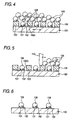
- FIG.1 to FIG.6 are step views describing a conductive ball mounting method in the related-art.
- a conductive ball mounting method in the related-art will be described with reference to FIG.1 to FIG.6 hereunder.
- a flux 102 is formed on a plurality of pads 101 provided on a substrate 100, and also a resist film 103 is formed on portions of the substrate 100 positioned between a plurality of pads 101.
- the mask 106 having a plurality of openings 106A is fixed on the resist film 103.
- the openings 106A are formed to expose the pads 101.
- a plurality of conductive balls 108 are disposed on the mask 106.
- one conductive ball 108 is mounted on the pads 101 on which the flux 102 is formed respectively by vibrating the substrate 100.
- step shown in FIG.5 extra conductive balls 108 that have not been mounted on the pads 101 are removed by sweeping an upper surface of the mask 106 by a squeegee 110. Then, in steps shown in FIG.6 , the mask 106 is removed. Accordingly, the substrate 100 having the conductive balls 108 on the pads 101 is formed ( see e.g., JP-A-11-297886 ).
- the step of mounting one conductive ball 108 on the pads 101 on which the flux 102 is formed respectively and the step of removing the extra conductive balls 108 by sweeping an upper surface of the mask 106 by the squeegee 110 are performed separately. Therefore, such a problem existed that it is difficult to improve productivity in the step of mounting the conductive ball 108 on the pads 101 and the step of removing the extra conductive balls 108.
- US 2007/145103 and WO 2002/01930 describe apparatuses for use in mounting electrically conducting particles on a substrate having an array of tacky and non-tacky areas.
- the associated methods involve use of first and second electrode plates with a substrate therebetween, the plates having applied thereto a direct current potential.
- EP 2017882 describes a method of mounting conductive balls on pads on a substrate.
- the method includes: (a) placing the substrate having the pads coated with an adhesive over a container for containing the conductive balls therein and whose top surface is open such that the pads face the top surface of the container; and (b) throwing up the conductive balls in the container by moving the container up and down at a given stroke, thereby allowing the conductive balls to adhere to the adhesive coated on the pads. Step (b) is repeatedly performed.
- JP-A-2-102538 discloses another conductive ball mounting method.
- a conductive layer on which a solder bump is formed is formed on one surface of a circuit substrate and also a solder-flux layer is formed on the one surface of the circuit substrate.
- a spacer is formed on the solder-flux layer and a mask having openings is formed on the spacer.
- the circuit substrate is disposed on a solder ball container for accommodating solder balls such that the one surface of the circuit substrate opposes to an opening formed in the solder ball container.
- the solder balls are mounted on the circuit substrate by vibrating the solder ball container hard (see Fig. 1 of JP-A-2-102538 ).
- a conductive ball mounting apparatus according to independent claim 1 and a method for mounting one conductive ball according to independent claim 4 are provided.
- One or more exemplary embodiments of the present invention provide a conductive ball mounting apparatus and a conductive ball mounting method that can improve productivity by reducing a processing time required for the step of mounting a conductive ball on a plurality of pads respectively and the step of removing extra conductive balls.
- a mask may have a plurality of through portions corresponding to positions where the plurality of pads are formed, and the mask may be provided to the substrate such that each of the pads is exposed from the plurality of through portions, and a diameter of the through portions may be set to a size capable of passing only one conductive ball. Therefore, it can be prevented that the plurality of conductive balls are mounted on one pad.
- the conductive ball mounting apparatus further comprises:
- the method further comprises:
- productivity can be improved by reducing a processing time in the step of mounting conductive balls on a plurality of pads and the step of removing extra conductive balls.
- the substrate is disposed over the conductive ball container with a space therebetween, so that defect such as displacement of solder balls can be suppressed.
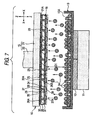
- FIG.7 is a sectional view of a conductive ball mounting apparatus according to a first embodiment of the present invention.
- a plurality of conductive balls 14 are caused to move up the lower side of a substrate 18 held by a substrate holder 15.
- Z direction denotes the vertical direction
- X direction denotes the direction that intersects orthogonally with the Z direction.
- a conductive ball mounting apparatus 10 of the first embodiment includes a stage 11, a vibrating unit 12 as a conductive ball supplying unit, a conductive ball container 13, a plurality of conductive balls 14, and the substrate holder 15 for holding the substrate 18.
- the substrate 18 is constructed such that a plurality of substrates 25 are formed on a plate-like substrate main body 26. That is, the substrate 18 is an aggregate of the plurality of substrates 25 prior to diving into individual pieces.
- a glass epoxy resin may be used as the substrate main body 26.
- the substrate 25 has the substrate main body 26, through vias 28, upper wirings 29, pads 31, 35, solder resists 32, 37, lower wirings 34, and adhesives 38.
- the through via 28 is provided to pass through the substrate main body 26. An upper end portion of the through via 28 is connected to the pad 31, and a lower end portion of the through via 28 is connected to the pad 35.
- the upper wirings 29 are provided on an upper surface 26A of the substrate main body 26.
- the upper wirings 29 are connected to the pads 31.
- the pads 31 are provided on portions, which correspond to positions where the through via 28 is formed, of the upper surface 26A of the substrate main body 26.
- the pad 31 is connected to the through vias 28 respectively.
- the pads 31 are provided to mount an electronic component (e.g., a passive component, or the like).
- the solder resist 32 is provided on the upper surface 26A of the substrate main body 26 to cover the upper wirings 29.
- the solder resist 32 has openings 32A to expose the pads 31.
- the lower wirings 34 are provided on a lower surface 26B of the substrate main body 26.
- the lower wirings 34 are connected to the pads 35.
- the pads 35 are provided on portions, which correspond to positions where the through via 28 is formed, of the lower surface 26B of the substrate main body 26.
- the pad 35 is connected to the through vias 28 respectively.
- the pads 35 are connected electrically to the pads 31 via the through vias 28.
- One conductive ball 14 serving as an external connection terminal of the substrate 25 is provided on the pad 35 via the adhesive 38.
- the solder resist 37 is provided on the lower surface 26B of the substrate main body 26 to cover the lower wirings 34.
- the solder resist 37 has openings 37A to expose the pads 35.
- the adhesive 38 is provided on the pads 35 to fill the openings 37A.
- the adhesive 38 is used to temporarily fix the conductive balls 14 that are caused to move up when the vibrating unit 12 vibrates the conductive ball container 13. As the adhesive 38, the flux, the solder paste may be used.
- the substrate 18 constructed as above is held by the substrate holder 15 such that a plurality of pads 35 on which the adhesive 38 is formed respectively are opposed to a plurality of conductive balls 14 exposed from openings 13A.
- the stage 11 supports the conductive ball container 13 via the vibrating unit 12.
- the vibrating unit 12 is provided on the stage 11.
- the vibrating unit 12 vibrates the conductive ball container 13 containing a plurality of conductive balls 14 to move up the plurality of conductive balls 14, and thus supplies the plurality of conductive balls 14 to the substrate 18 arranged over the conductive ball container 13.
- the vibrating unit 12 moves up the plurality of conductive balls 14 from the lower side of the substrate 18, extra conductive balls 14, which are not disposed on the pads 35 on which the adhesive 38 is formed, out of the plurality of moved up conductive balls 14 fall down on the conductive ball container 13. Therefore, the step of mounting the conductive ball 14 on the plurality of pads 35 respectively and the step of removing extra conductive balls 14 can be performed at the same time. As a result, a processing time required for the step of mounting the conductive ball 14 on the plurality of pads 35 respectively and the step of removing the extra conductive balls 14 can be shortened, and productivity can be improved.
- the conductive ball container 13 is provided to contain the plurality of conductive balls 14.
- the opening 13A for passing the plurality of conductive balls 14 moved up by the vibrating unit 12 through there is formed on the upper end portion of the conductive ball container 13.
- the plurality of conductive balls 14 passing through the conductive ball container 13 reach the substrate 18 and are disposed on the pads 35 on which the adhesive 38 is formed respectively.
- a metal may be used as the material of the conductive ball container 13, a metal may be used.
- a plurality of conductive balls 14 are contained in the conductive ball container 13.
- the conductive balls 14 act as the external connection terminals of the substrate 25.
- a solder ball may be used as the conductive ball 14.
- a diameter of the conductive ball 14 may be set to 10 ⁇ m to 100 ⁇ m, for example.
- the substrate holder 15 is disposed over the conductive ball container 13.
- the substrate holder 15 has a substrate holding portion 21, and a support 22.
- the substrate holding portion 21 is disposed such that its lower surface 21A faces the opening 13A of the conductive ball container 13.
- the substrate holding portion 21 is formed into a plate shape.
- the substrate holding portion 21 holds the substrate 18 on its lower surface 21A.
- suction, mechanical holding e.g., clamping
- a distance D1 between the adhesives 38 of the substrate 18 held by the substrate holding portion 21 and the plurality of conductive balls 14 contained in the conductive ball container 13 may be set to 1 mm, for example.
- the support 22 is provided to support the substrate holding portion 21.
- the conductive ball mounting apparatus includes: the conductive ball container 13 for containing a plurality of conductive balls 14 therein and also having the opening 13A to supply the plurality of conductive balls 14; the substrate holder 15 disposed over the conductive ball container 13 to face the opening 13A and for holding the substrate 18 such that a plurality of conductive balls 14 and a plurality of pads 35 are opposed to each other; and the vibrating unit 12 for moving up the plurality of conductive balls 14.
- the step of mounting the conductive ball 14 on the plurality of pads 35 respectively and the step of removing extra conductive balls 14 may be carried out simultaneously.
- a processing time required for the step of mounting the conductive ball 14 on the plurality of pads 35 respectively and the step of removing the extra conductive balls 14 can be shortened, and thus productivity can be improved.
- FIG.8 to FIG.14 are step views describing a conductive ball mounting method using the conductive ball mounting apparatus according to the first embodiment of the present invention.
- the same reference symbols are denoted to the same constituent portions as the configuration shown in FIG.7 .
- "A" denotes a position where the substrate 18 is divided into individual pieces (referred to as a "cut position A” hereinafter).
- the substrate 18 where the adhesive 38 is provided on a plurality of pads 35 respectively is formed by the well-known approach.
- steps shown in FIG.9 a plurality of conductive balls 14 are filled in the conductive ball container 13.
- the substrate 18 is held by the substrate holding portion 21 such that the substrate 18 is disposed over the conductive ball container 13 with a space therebetween.
- the substrate holding portion 21 is disposed over the plurality of conductive balls 14 such that the plurality of conductive balls 14 and the plurality of pads 35 on which the adhesive 38 is provided respectively face each other (substrate disposing step).
- the plurality of conductive balls 14 are provided to the plurality of pads 35 by vibrating the conductive ball container 13 by means of the vibrating unit 12 to move up the plurality of conductive balls 14 contained in the conductive ball container 13 (conductive ball providing step).
- the substrate 18 on which the conductive balls 14 are mounted is released from the substrate holding portion 21. Then, the conductive balls 14 and the pads 35 are joined together by heating a structure shown in FIG.13 , and then the adhesive 38 is cleaned.
- the plurality of conductive balls 14 are moved up to the lower side of the substrate 18 being held such that the plurality of conductive balls 14 and a plurality of pads 35 on which the adhesive 38 is provided respectively face each other.
- the extra conductive balls 14, which are not disposed on the pads 35 on which the adhesive 38 is formed, out of the plurality of raised conductive balls 14 fall down on the conductive ball container 13. Therefore, the step of mounting the conductive ball 14 on the plurality of pads 35 respectively and the step of removing extra conductive balls 14 can be carried out at the same time.
- a processing time required for the step of mounting the conductive ball 14 on the plurality of pads 35 respectively and the step of removing the extra conductive balls 14 can be shortened, and thus productivity can be improved.
- the vibrating unit 12 is used as the conductive ball supplying unit is described by way of example.
- any means may be employed as the conductive ball supplying unit if such means can move up the plurality of conductive balls 14.
- an air supplying unit for moving up the plurality of conductive balls 14 by supplying an air may be employed.
- FIG.15 is a sectional view of a conductive ball mounting apparatus according to a second embodiment of the present invention.
- a conductive ball mounting apparatus according to a second embodiment of the present invention.
- FIG.15 such a situation is illustrated that a plurality of conductive balls 14 are moved up to the lower side of the substrate 18 held by the substrate holder 15.
- the same reference symbols are denoted to the same constituent portions as those of the conductive ball mounting apparatus 10 in the first embodiment.
- a conductive ball mounting apparatus 45 of the second embodiment is constructed similarly to the conductive ball mounting apparatus 10 except that a mask 46 is provided to the configuration of the conductive ball mounting apparatus 10 in the first embodiment. Also, the mask 46 is disposed over the conductive ball container 13 with a space therebetween.
- the mask 46 is fixed to the substrate 18 via a resist film 47 formed on the solder resist 37.
- the mask 46 has through portions 46A.
- a plurality of through portions 46A are formed to pass through portions, which correspond to positions where the pad 35 is formed respectively, of the mask 46.
- the through portions 46A are formed to expose the pads 35.
- a diameter R1 of the through portion 46A is set to a size through which only one conductive ball 14 can pass (a size larger slightly than a diameter of the conductive ball 14). Concretely, when a diameter of the conductive ball 14 is 100 ⁇ m, a diameter R1 of the through portion 46A can be set to 120 ⁇ m, for example.
- the material of the mask 46 a metal may be used.
- the mask 46 having the plurality of through portions 46A in portions corresponding to positions where a plurality of pads 35 are formed is fixed to the substrate 18, and also a diameter R1 of the through portion 46A is set to a size through which only one conductive ball 14 can pass. Therefore, such a situation can be prevented that the plurality of conductive balls 14 are disposed on one pad 35 on which the adhesive 38 is formed.
- the conductive ball 14 can be mounted on the plurality of pads 35 respectively by the similar approach to the method of mounting the conductive ball 14 described in the first embodiment.
- the mask 46 having the plurality of through portions 46A in portions corresponding to positions where the plurality of pads 35 are formed is fixed to the substrate 18, and then the plurality of conductive balls 14 are moved up. Therefore, a diameter R1 of the through portion 46A is set to a size through which only one conductive ball 14 can pass. As a result, such a situation can be prevented that the plurality of conductive balls 14 are mounted on one pad 35 on which the adhesive 38 is formed.
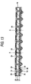
- FIG.16 is a sectional view of a conductive ball mounting apparatus according to a third embodiment of the present invention.
- a conductive ball mounting apparatus according to a third embodiment of the present invention.
- FIG.16 such a situation is illustrated that a plurality of conductive balls 14 are moved up to the lower side of the substrate 18 held by the substrate holder 15.
- the same reference symbols are denoted to the same constituent portions as those of the conductive ball mounting apparatus 45 in the second embodiment.
- a conductive ball mounting apparatus 50 is constructed similarly to the conductive ball mounting apparatus 45 except that a potential difference generating unit 51 and insulating members 52A, 52B are provided to the configuration of the conductive ball mounting apparatus 45 in the second embodiment.
- the potential difference generating unit 51 has a power supply 54 and wirings 56 to 58.
- the power supply 54 has a plus terminal 54A and a minus terminal 54B.
- the plus terminal 54A is connected electrically to the substrate 18 via the wiring 56. Accordingly, the substrate 18 is set to a plus potential.
- the minus terminal 54B is connected to a ground via the wiring 57. Accordingly, the minus terminal 54B is set to a ground potential.
- One end portion of the wiring 56 is connected to the substrate 18 whereas the other end is connected to the plus terminal 54A.
- One end portion of the wiring 57 is connected to the minus terminal 54B whereas the other end is connected to a ground.
- One end portion of the wiring 58 is connected to the wiring 57 whereas the other end is connected to the conductive ball container 13. Accordingly, the conductive ball container 13 and a plurality of conductive balls 14 contained in the conductive ball container 13 are set to a ground potential.
- the potential difference generating unit 51 constructed as above is provided to generate a potential difference between the plurality of conductive balls 14 contained in the conductive ball container 13 and the substrate 18.
- a potential difference generated between a plurality of conductive balls 14 and the substrate 18 may be set such that an electrical attractive force generated between the plurality of conductive balls 14 and the substrate 18 by the potential difference exceeds a gravity applied to the conductive balls 14.
- the potential difference generated between the plurality of conductive balls 14 and the substrate 18 may be set to several hundreds V to tens of thousands V, for example.
- the potential difference generating unit 51 for generating a potential difference between the plurality of conductive balls 14 contained in the conductive ball container 13 and the substrate 18 is provided.
- the plurality of moved-up conductive balls 14 are attracted to the substrate 18 by an electrical attractive force.
- a processing time in the step of mounting the conductive ball 14 on the plurality of pads 35 respectively can be shortened.
- the insulating member 52A is provided between the vibrating unit 12 and the conductive ball container 13.
- the insulating member 52A is provided to make the charging of the plurality of conductive balls 14 contained in the conductive ball container 13 easy.
- the insulating member 52B is provided between the substrate holding portion 21 and the support 22.
- the insulating member 52B is provided to insulate the substrate holding portion 21 and the support 22 mutually.
- the potential difference generating unit 51 for generating the potential difference between the plurality of conductive balls 14 contained in the conductive ball container 13 and the substrate 18 is provided.
- the plurality of moved-up conductive balls 14 are attracted to the substrate 18 by an electrical attractive force.
- a processing time required for the step of mounting the conductive ball 14 on a plurality of pads 35 respectively can be reduced.
- the conductive ball 14 can be mounted on the plurality of pads 35 respectively by the similar approach to the method of mounting the conductive ball 14 in the first embodiment, except that a potential difference is generated between the plurality of conductive balls 14 contained in the conductive ball container 13 and the substrate 18 (the potential difference generating step) in the steps shown in FIG.10 and FIG.11 in the first embodiment.
- the plurality of conductive balls 14 are moved up after a potential difference is generated between the plurality of conductive balls 14 contained in the conductive ball container 13 and the substrate 18 (the potential difference generating step). Therefore, the plurality of raised conductive balls 14 are attracted to the substrate 18 by an electrical attractive force. As a result, a processing time in the step of mounting the conductive ball 14 on the plurality of pads 35 respectively can be reduced.
- the case where the plurality of conductive balls 14 contained in the conductive ball container 13 are set to a ground potential and the substrate 18 is set to a plus potential is described as an example. But the substrate 18 may be set to a ground potential and the plurality of conductive balls 14 may be set to a plus potential.
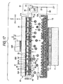
- FIG.17 is a sectional view of a conductive ball mounting apparatus according to a fourth embodiment of the present invention.
- a conductive ball mounting apparatus according to a fourth embodiment of the present invention.
- FIG.17 such a situation is illustrated that a plurality of conductive balls 14 are moved up to the lower side of the substrate 18 held by the substrate holder 15.
- the same reference symbols are denoted to the same constituent portions as those of the conductive ball mounting apparatus 50 in the third embodiment.
- a conductive ball mounting apparatus 60 of the fourth embodiment is constructed similarly to the conductive ball mounting apparatus 50 except that a charging unit 61 is further provided to the configuration of the conductive ball mounting apparatus 50 in the third embodiment.
- a wiring is used as the charging unit 61will be described below.
- One end portion of the charging unit 61 is connected to the wiring 57 whereas the other end portion is connected to the mask 46. Accordingly, the mask 46 is set to a ground potential that is substantially equal to a potential of the plurality of conductive balls 14 contained in the conductive ball container 13.
- the potential difference generating unit 51 for generating a potential difference between the plurality of conductive balls 14 contained in the conductive ball container 13 and the substrate 18 and the charging unit 61 for making a potential of the mask 46 substantially equal to a potential of the plurality of conductive balls 14 contained in the conductive ball container 13. Therefore, the plurality of moved-up conductive balls 14 are attracted to the pads 35 by an electrical attractive force. As a result, a processing time in the step of mounting the conductive ball 14 on the plurality of pads 35 respectively can be further shortened.
- the conductive ball 14 can be mounted on the plurality of pads 35 respectively by the similar approach to the method of mounting the conductive ball 14 in the first embodiment except that a potential difference is generated between the plurality of conductive balls 14 contained in the conductive ball container 13 and the substrate 18 (the potential difference generating step) and a potential of the mask 46 is made substantially equal to a potential of the plurality of conductive balls 14 contained in the conductive ball container 13 (the mask charging step), in the steps shown in FIG.10 and FIG.11 in the first embodiment.
- the plurality of conductive balls 14 are moved up after a potential difference is generated between the plurality of conductive balls 14 contained in the conductive ball container 13 and the substrate 18 (the potential difference generating step) and a potential of the mask 46 is made substantially equal to a potential of the plurality of conductive balls 14 contained in the conductive ball container 13 (the mask charging step). Therefore, the plurality of moved-up conductive balls 14 are attracted to the pads 35 by an electrical attractive force. As a result, a processing time in the step of mounting the conductive ball 14 on the plurality of pads 35 respectively can be further reduced.
- FIG.18 is a sectional view of a conductive ball mounting apparatus according to a fifth embodiment of the present invention.
- a conductive ball mounting apparatus according to a fifth embodiment of the present invention.
- FIG.18 such a situation is illustrated that a plurality of conductive balls 14 are sprayed to the substrate 18, on which the mask 46 is provided, from the direction that intersects orthogonally with the vertical direction (Z- direction).
- the same reference symbols are denoted to the same constituent portions as those of the conductive ball mounting apparatus 45 in the second embodiment.
- a conductive ball mounting apparatus 70 of the fifth embodiment is constructed similarly to the conductive ball mounting apparatus 45, except that a supporting table 71, a conductive ball container 72, an air supplying unit 73 as the conductive ball supplying unit, and a conductive ball recovering container 74 are provided instead of the stage 11, the vibrating unit 12, and the conductive ball container 13 provided to the conductive ball mounting apparatus 45 of the second embodiment and except that the substrate 18 is held by the substrate holder 15 such that openings 76A of the conductive ball container 72 and the pads 35 face each other in a direction perpendicular to the vertical direction (Z, Z direction).
- the supporting table 71 is provided to support the conductive ball container 72 and the air supplying unit 73.
- the conductive ball container 72 has a front plate 76 and a rear plate 77.
- the conductive ball container 72 is disposed such that the front plate 76 faces a plurality of pads 35.
- the front plate 76 has a plurality of openings 76A.
- the openings 76A are formed to pass through portions of the front plate 76, which face to the pads 35.
- a diameter of the conductive ball 14 is 100 ⁇ m
- a diameter R2 of the opening 76A may be set to 150 ⁇ m, for example.
- a distance D2 between the front plate 76 and the adhesive 38 may be set to 1 mm, for example.
- the rear plate 77 has a plurality of air introduction ports 77A.
- the air introduction ports 77A are formed to pass through portions, which face to the openings 76A, of the rear plate 77.
- the plurality of air introduction ports 77A are provided to introduce an air supplied from the air supplying unit 73 into the conductive ball container 72.
- the air supplying unit 73 is provided on the supporting table 71 and contacts the rear plate 77 of the conductive ball container 72.
- the air supplying unit 73 is the unit that supplies an air into the conductive ball container 72 via the air introduction ports 77A.
- the air supplying unit 73 supplies an air into the conductive ball container 72 to spray a plurality of conductive balls 14 to the substrate 18, on which the mask 46 is provided, (concretely, the plurality of pads 35) via the openings 76A in such a manner that one conductive ball 14 is mounted on the plurality of pads 35 respectively.
- the conductive ball recovering container 74 is disposed below the substrate 18. An upper end portion of the conductive ball recovering container 74 is open. The conductive ball recovering container 74 is provided to recover the extra conductive balls 14 that are not disposed on the pads 35 and fall down in the vertical direction by virtue of gravity. In this manner, the recovered conductive balls 14 can be reused by providing the conductive ball recovering container 74.
- the conductive ball mounting apparatus includes: the conductive ball container 72 for containing the plurality of conductive balls 14 and having the plurality of openings 76A to supply the plurality of conductive balls 14; the substrate holder 15 for holding the substrate 18 such that the openings 76A of the conductive ball container 72 and the pads 35 face each other in a direction perpendicular to the vertical direction (Z direction); and the air supplying unit 73 for spraying the plurality of conductive balls 14 to the plurality of pads 35. Therefore, the extra conductive balls 14, which are not disposed on the pads 35 on which the adhesive 38 is formed respectively, out of the plurality of conductive balls 14 sprayed to the substrate 18 fall down in the vertical direction by virtue of gravity. As a result, the step of mounting the conductive ball 14 on the plurality of pads 35 respectively and the step of removing the extra conductive balls 14 can be carried out simultaneously.
- a processing time required for the step of mounting the conductive ball 14 on the plurality of pads 35 respectively and the step of removing the extra conductive balls 14 can be shortened, and productivity can be improved.
- the conductive ball 14 can be mounted on the plurality of pads 35 respectively by the similar approach to the method of mounting the conductive balls 14 described in the first embodiment, except that the plurality of conductive balls 14 are supplied to the substrate 18 by an air supplied from the air supplying unit 73 in the steps shown in FIG.11 in the first embodiment.
- the substrate 18 is held such that the openings 76A and the pads 35 face each other in a direction perpendicular to the vertical direction (Z direction), and then the plurality of conductive balls 14 are sprayed to the plurality of pads 35 by the air supplying unit 73. Therefore, the extra conductive balls 14, which are not disposed on the pads 35, out of the plurality of conductive balls 14 sprayed to the substrate 18 fall down in the vertical direction by virtue of gravity. As a result, the step of mounting the conductive ball 14 on the plurality of pads 35 respectively and the step of removing the extra conductive balls 14 can be performed at the same time.
- a time required for the step of mounting the conductive ball 14 on the plurality of pads 35 respectively and the step of removing the extra conductive balls 14 can be reduced shorter than the related-art.
- productivity can be improved in the step of mounting the conductive ball 14 on the plurality of pads 35 respectively and the step of removing the extra conductive balls 14.
- the potential difference generating unit 51 (see FIG. 16 ) described in the third embodiment may be provided to the conductive ball mounting apparatus 70 of the present embodiment. In this case, the similar advantages to those of the conductive ball mounting apparatus 50 in the third embodiment can be achieved.
- the potential difference generating unit 51 (see FIG.16 ) described in the third embodiment and the charging unit 61 (see FIG.17 ) described in the fourth embodiment may be provided to the conductive ball mounting apparatus 70 of the present embodiment.
- the similar advantages to those of the conductive ball mounting apparatus 60 in the fourth embodiment can be achieved.
- FIG.19 is a sectional view of a conductive ball mounting apparatus according to a sixth embodiment of the present invention.
- a conductive ball mounting apparatus according to a sixth embodiment of the present invention.
- FIG.19 such a situation is illustrated that a plurality of conductive balls 14 are moved up to the lower side of the substrate 18 held by the substrate holder 15.
- the same reference symbols are denoted to the same constituent portions as those of the conductive ball mounting apparatus 45 in the second embodiment.
- a conductive ball mounting apparatus 80 of the sixth embodiment is constructed similarly to the conductive ball mounting apparatus 45, except that a plate 81 and a containing stage 82 are provided instead of the mask 46 and the stage 11 provided to the conductive ball mounting apparatus 45 in the second embodiment and except that the resist film 47 provided in the conductive ball mounting apparatus 45 is removed from the constituent elements.
- the containing stage 82 has a containing portion 82A to contain the vibrating unit 12 and the conductive ball container 13 therein.
- the containing stage 82 contacts the lower end portion of the vibrating unit 12.
- the containing stage 82 supports the conductive ball container 13 via the vibrating unit 12.
- the plate 81 is provided to the containing stage 82, and is disposed over the conductive ball container 13.
- the plate 81 has a plurality of through portions 81A.
- the through portions 81A are formed to pass through portions, which face to the pads 35, of the plate 81.
- the plate 81 having the plurality of through portions 81A is the mask used to emit the conductive balls 14 toward the adhesive 38 being formed on the pads 35 respectively.
- a diameter of the conductive ball 14 is 100 ⁇ m
- a diameter of the through portion 81A may be set to 120 ⁇ m, for example.
- As the material of the plate 81 a metal may be used.
- the containing stage 82 for containing the vibrating unit 12 and the conductive ball container 13 therein is provided, and also the plate 81 having the through portions 81A that emit the conductive balls 14 toward the adhesive 38 being formed on the pads 35 respectively is provided to the containing stage 82. Therefore, the conductive balls 14 can be mounted more easily than the case where the conductive ball 14 is mounted on the pads 35, on which the adhesive 38 is formed respectively, by fitting the mask 46 on the substrate 18 via the resist film 47, and also productivity can be improved in the conductive ball mounting step.
- the method of mounting the conductive ball 14 of the present embodiment can be carried out by the similar approach to the method of mounting the conductive ball 14 of the second embodiment.
- the method of mounting the conductive ball 14 of the present embodiment can achieve the similar advantages to those of the method of mounting the conductive balls 14 in the second embodiment.
- the present invention is applicable to the conductive ball mounting apparatus and the conductive ball mounting method for mounting the conductive balls on the substrate having the plurality of pads on which an adhesive is formed thereon.
Landscapes
- Engineering & Computer Science (AREA)
- Manufacturing & Machinery (AREA)
- Microelectronics & Electronic Packaging (AREA)
- Computer Hardware Design (AREA)
- Power Engineering (AREA)
- Ceramic Engineering (AREA)
- Physics & Mathematics (AREA)
- Condensed Matter Physics & Semiconductors (AREA)
- General Physics & Mathematics (AREA)
- Electric Connection Of Electric Components To Printed Circuits (AREA)
Abstract
Description
- The present disclosure relates to a conductive ball mounting apparatus and a conductive ball mounting method and, more particularly, a conductive ball mounting apparatus and a conductive ball mounting method for mounting conductive ball(s) on a substrate such as a wiring substrate, a wafer, or the like. More particularly, the substrate generally has a plurality of pads on which an adhesive is formed thereon, and on which the conductive balls are generally mounted.
-
FIG.1 to FIG.6 are step views describing a conductive ball mounting method in the related-art. - A conductive ball mounting method in the related-art will be described with reference to
FIG.1 to FIG.6 hereunder. At first, in steps shown inFIG.1 , aflux 102 is formed on a plurality ofpads 101 provided on asubstrate 100, and also aresist film 103 is formed on portions of thesubstrate 100 positioned between a plurality ofpads 101. - Then, in steps shown in
FIG.2 , themask 106 having a plurality ofopenings 106A is fixed on theresist film 103. Theopenings 106A are formed to expose thepads 101. - Then, in steps shown in
FIG.3 , a plurality ofconductive balls 108 are disposed on themask 106. Then, in steps shown inFIG.4 , oneconductive ball 108 is mounted on thepads 101 on which theflux 102 is formed respectively by vibrating thesubstrate 100. - Then, in steps shown in
FIG.5 , extraconductive balls 108 that have not been mounted on thepads 101 are removed by sweeping an upper surface of themask 106 by asqueegee 110. Then, in steps shown inFIG.6 , themask 106 is removed. Accordingly, thesubstrate 100 having theconductive balls 108 on thepads 101 is formed (see e.g.,JP-A-11-297886 - However, in the method of mounting the
conductive ball 108 in the related-art, the step of mounting oneconductive ball 108 on thepads 101 on which theflux 102 is formed respectively and the step of removing the extraconductive balls 108 by sweeping an upper surface of themask 106 by thesqueegee 110 are performed separately. Therefore, such a problem existed that it is difficult to improve productivity in the step of mounting theconductive ball 108 on thepads 101 and the step of removing the extraconductive balls 108. -
US 2007/145103 andWO 2002/01930 -
EP 2017882 describes a method of mounting conductive balls on pads on a substrate. The method includes: (a) placing the substrate having the pads coated with an adhesive over a container for containing the conductive balls therein and whose top surface is open such that the pads face the top surface of the container; and (b) throwing up the conductive balls in the container by moving the container up and down at a given stroke, thereby allowing the conductive balls to adhere to the adhesive coated on the pads. Step (b) is repeatedly performed. - In addition, Japanese Patent Application Publication:
JP-A-2-102538 JP-A-2-102538 Fig. 1 ofJP-A-2-102538 - However, in the conductive ball mounting method disclosed in the related-art, rapid vibration is required to mount the solder balls on the openings of the mask. In this case, force caused by the rapid vibration is also applied to the circuit substrate (the mask). Especially, upon using a large substrate, a thin substrate or small balls whose diameter is 100 µm or less, thickness of the mask becomes thin and thus the mask is more likely to vibrate. Therefore, defect such as displacement of the solder balls is generated by vibration of the mask (the circuit substrate).
- In view of the above, a conductive ball mounting apparatus according to independent claim 1 and a method for mounting one conductive ball according to independent claim 4 are provided.
One or more exemplary embodiments of the present invention provide a conductive ball mounting apparatus and a conductive ball mounting method that can improve productivity by reducing a processing time required for the step of mounting a conductive ball on a plurality of pads respectively and the step of removing extra conductive balls. - According to embodiments of the present invention, the extra conductive balls, which are not disposed on the pads on which the adhesive is formed, out of the plurality of moved-up conductive balls fall down on the conductive ball container. Therefore, the step of mounting the conductive ball on the plurality of pads respectively and the step of removing extra conductive balls can be carried out simultaneously. As a result, a processing time required for the step of mounting the conductive ball on the plurality of pads respectively and the step of removing the extra conductive balls can be shortened, and thus productivity can be improved.
- According to one or more embodiments of the apparatus of the present invention, a mask may have a plurality of through portions corresponding to positions where the plurality of pads are formed, and the mask may be provided to the substrate such that each of the pads is exposed from the plurality of through portions, and a diameter of the through portions may be set to a size capable of passing only one conductive ball.
Therefore, it can be prevented that the plurality of conductive balls are mounted on one pad. - According to one or more embodiments of the apparatus of the present invention, the conductive ball mounting apparatus further comprises:
- a conductive ball recovering container for recovering extra conductive balls that are not disposed on the pads and fall down in the gravity direction, the conductive ball recovering container being disposed below the substrate in the gravity direction.
- According to an embodiment of the method of the present invention, the method further comprises:
- (c) providing a mask having a plurality of through portions corresponding to positions where a plurality of pads are formed, before step (a).
- According to one or more exemplary embodiments of the present invention, productivity can be improved by reducing a processing time in the step of mounting conductive balls on a plurality of pads and the step of removing extra conductive balls.
- According to one or more exemplary embodiments of the present invention, the substrate is disposed over the conductive ball container with a space therebetween, so that defect such as displacement of solder balls can be suppressed.
- Other aspects and advantages of the invention will be apparent from the following description, the drawings and the claims.
The invention will be better understood by reference to the following description of embodiments of the invention taken in conjunction with the accompanying drawings, wherein: -
FIG.1 is a step view (#1) describing a conductive ball mounting method in the related-art; -
FIG.2 is a step view (#2) describing the conductive ball mounting method in the related-art; -
FIG.3 is a step view (#3) describing the conductive ball mounting method in the related-art; -
FIG.4 is a step view (#4) describing the conductive ball mounting method in the related-art; -
FIG.5 is a step view (#5) describing the conductive ball mounting method in the related-art; -
FIG.6 is a step view (#6) describing the conductive ball mounting method in the related-art; -
FIG.7 is a sectional view of a conductive ball mounting apparatus according to a first embodiment of the present invention; -
FIG.8 is a step view (#1) describing a conductive ball mounting method using the conductive ball mounting apparatus according to the first embodiment of the present invention; -
FIG.9 is a step view (#2) describing the conductive ball mounting method using the conductive ball mounting apparatus according to the first embodiment of the present invention; -
FIG.10 is a step view (#3) describing the conductive ball mounting method using the conductive ball mounting apparatus according to the first embodiment of the present invention; -
FIG.11 is a step view (#4) describing the conductive ball mounting method using the conductive ball mounting apparatus according to the first embodiment of the present invention; -
FIG.12 is a step view (#5) describing the conductive ball mounting method using the conductive ball mounting apparatus according to the first embodiment of the present invention; -
FIG.13 is a step view (#6) describing the conductive ball mounting method using the conductive ball mounting apparatus according to the first embodiment of the present invention; -
FIG.14 is a step view (#7) describing the conductive ball mounting method using the conductive ball mounting apparatus according to the first embodiment of the present invention; -
FIG.15 is a sectional view of a conductive ball mounting apparatus according to a second embodiment of the present invention; -
FIG.16 is a sectional view of a conductive ball mounting apparatus according to a third embodiment of the present invention; -
FIG.17 is a sectional view of a conductive ball mounting apparatus according to a fourth embodiment of the present invention; -
FIG.18 is a sectional view of a conductive ball mounting apparatus according to a fifth embodiment of the present invention; and -
FIG.19 is a sectional view of a conductive ball mounting apparatus according to a sixth embodiment of the present invention. - Exemplary embodiments of the present invention will be described with reference to the drawings hereinafter.
-
FIG.7 is a sectional view of a conductive ball mounting apparatus according to a first embodiment of the present invention. InFIG.7 , such a situation is illustrated that a plurality ofconductive balls 14 are caused to move up the lower side of asubstrate 18 held by asubstrate holder 15. Also, inFIG.7 , Z direction denotes the vertical direction, and X direction denotes the direction that intersects orthogonally with the Z direction. - By reference to
FIG.7 , a conductiveball mounting apparatus 10 of the first embodiment includes astage 11, a vibratingunit 12 as a conductive ball supplying unit, aconductive ball container 13, a plurality ofconductive balls 14, and thesubstrate holder 15 for holding thesubstrate 18. - At first, for brief description, a structure of the
substrate 18 held by thesubstrate holder 15 will be described hereunder. Thesubstrate 18 is constructed such that a plurality ofsubstrates 25 are formed on a plate-like substratemain body 26. That is, thesubstrate 18 is an aggregate of the plurality ofsubstrates 25 prior to diving into individual pieces. As the substratemain body 26, a glass epoxy resin may be used. - The
substrate 25 has the substratemain body 26, throughvias 28,upper wirings 29,pads lower wirings 34, andadhesives 38. The through via 28 is provided to pass through the substratemain body 26. An upper end portion of the through via 28 is connected to thepad 31, and a lower end portion of the through via 28 is connected to thepad 35. - The
upper wirings 29 are provided on anupper surface 26A of the substratemain body 26. Theupper wirings 29 are connected to thepads 31. Thepads 31 are provided on portions, which correspond to positions where the through via 28 is formed, of theupper surface 26A of the substratemain body 26. Thepad 31 is connected to the throughvias 28 respectively. Thepads 31 are provided to mount an electronic component (e.g., a passive component, or the like). The solder resist 32 is provided on theupper surface 26A of the substratemain body 26 to cover theupper wirings 29. The solder resist 32 hasopenings 32A to expose thepads 31. - The
lower wirings 34 are provided on alower surface 26B of the substratemain body 26. Thelower wirings 34 are connected to thepads 35. Thepads 35 are provided on portions, which correspond to positions where the through via 28 is formed, of thelower surface 26B of the substratemain body 26. Thepad 35 is connected to the throughvias 28 respectively. Thepads 35 are connected electrically to thepads 31 via the throughvias 28. Oneconductive ball 14 serving as an external connection terminal of thesubstrate 25 is provided on thepad 35 via the adhesive 38. - The solder resist 37 is provided on the
lower surface 26B of the substratemain body 26 to cover thelower wirings 34. The solder resist 37 hasopenings 37A to expose thepads 35. The adhesive 38 is provided on thepads 35 to fill theopenings 37A. The adhesive 38 is used to temporarily fix theconductive balls 14 that are caused to move up when the vibratingunit 12 vibrates theconductive ball container 13. As the adhesive 38, the flux, the solder paste may be used. - The
substrate 18 constructed as above is held by thesubstrate holder 15 such that a plurality ofpads 35 on which the adhesive 38 is formed respectively are opposed to a plurality ofconductive balls 14 exposed fromopenings 13A. - The
stage 11 supports theconductive ball container 13 via the vibratingunit 12. The vibratingunit 12 is provided on thestage 11. The vibratingunit 12 vibrates theconductive ball container 13 containing a plurality ofconductive balls 14 to move up the plurality ofconductive balls 14, and thus supplies the plurality ofconductive balls 14 to thesubstrate 18 arranged over theconductive ball container 13. - Since such the vibrating
unit 12 moves up the plurality ofconductive balls 14 from the lower side of thesubstrate 18, extraconductive balls 14, which are not disposed on thepads 35 on which the adhesive 38 is formed, out of the plurality of moved upconductive balls 14 fall down on theconductive ball container 13. Therefore, the step of mounting theconductive ball 14 on the plurality ofpads 35 respectively and the step of removing extraconductive balls 14 can be performed at the same time. As a result, a processing time required for the step of mounting theconductive ball 14 on the plurality ofpads 35 respectively and the step of removing the extraconductive balls 14 can be shortened, and productivity can be improved. - The
conductive ball container 13 is provided to contain the plurality ofconductive balls 14. Theopening 13A for passing the plurality ofconductive balls 14 moved up by the vibratingunit 12 through there is formed on the upper end portion of theconductive ball container 13. The plurality ofconductive balls 14 passing through theconductive ball container 13 reach thesubstrate 18 and are disposed on thepads 35 on which the adhesive 38 is formed respectively. As the material of theconductive ball container 13, a metal may be used. - A plurality of
conductive balls 14 are contained in theconductive ball container 13. Theconductive balls 14 act as the external connection terminals of thesubstrate 25. As theconductive ball 14, a solder ball may be used. Also, when the solder ball is used as theconductive ball 14, a diameter of theconductive ball 14 may be set to 10 µm to 100 µm, for example. - The
substrate holder 15 is disposed over theconductive ball container 13. Thesubstrate holder 15 has asubstrate holding portion 21, and asupport 22. Thesubstrate holding portion 21 is disposed such that itslower surface 21A faces theopening 13A of theconductive ball container 13. Thesubstrate holding portion 21 is formed into a plate shape. Thesubstrate holding portion 21 holds thesubstrate 18 on itslower surface 21A. As the method of holding thesubstrate 18, suction, mechanical holding (e.g., clamping) may be used. Also, a distance D1 between theadhesives 38 of thesubstrate 18 held by thesubstrate holding portion 21 and the plurality ofconductive balls 14 contained in theconductive ball container 13 may be set to 1 mm, for example. Thesupport 22 is provided to support thesubstrate holding portion 21. - According to the present embodiment, the conductive ball mounting apparatus includes: the
conductive ball container 13 for containing a plurality ofconductive balls 14 therein and also having theopening 13A to supply the plurality ofconductive balls 14; thesubstrate holder 15 disposed over theconductive ball container 13 to face theopening 13A and for holding thesubstrate 18 such that a plurality ofconductive balls 14 and a plurality ofpads 35 are opposed to each other; and the vibratingunit 12 for moving up the plurality ofconductive balls 14. Thus, the extraconductive balls 14, which are not disposed on thepads 35 on which the adhesive 38 is formed, out of the plurality of moved-upconductive balls 14 fall down on theconductive ball container 13. Therefore, the step of mounting theconductive ball 14 on the plurality ofpads 35 respectively and the step of removing extraconductive balls 14 may be carried out simultaneously. As a result, a processing time required for the step of mounting theconductive ball 14 on the plurality ofpads 35 respectively and the step of removing the extraconductive balls 14 can be shortened, and thus productivity can be improved. -
FIG.8 to FIG.14 are step views describing a conductive ball mounting method using the conductive ball mounting apparatus according to the first embodiment of the present invention. InFIG.8 to FIG.14 , the same reference symbols are denoted to the same constituent portions as the configuration shown inFIG.7 . Also, inFIG.8 ,FIG.13 , andFIG.14 , "A" denotes a position where thesubstrate 18 is divided into individual pieces (referred to as a "cut position A" hereinafter). - The method of mounting the
conductive balls 14 using the conductiveball mounting apparatus 10 according to the first embodiment of the present invention will be described with reference toFIG.8 to FIG.14 hereunder. - At first, in steps shown in
FIG.8 , thesubstrate 18 where the adhesive 38 is provided on a plurality ofpads 35 respectively is formed by the well-known approach. Then, in steps shown inFIG.9 , a plurality ofconductive balls 14 are filled in theconductive ball container 13. - Then, in steps shown in
FIG.10 , thesubstrate 18 is held by thesubstrate holding portion 21 such that thesubstrate 18 is disposed over theconductive ball container 13 with a space therebetween. Thesubstrate holding portion 21 is disposed over the plurality ofconductive balls 14 such that the plurality ofconductive balls 14 and the plurality ofpads 35 on which the adhesive 38 is provided respectively face each other (substrate disposing step). - Then, in steps shown in
FIG.11 , the plurality ofconductive balls 14 are provided to the plurality ofpads 35 by vibrating theconductive ball container 13 by means of the vibratingunit 12 to move up the plurality ofconductive balls 14 contained in the conductive ball container 13 (conductive ball providing step). - Accordingly, the extra
conductive balls 14, which are not disposed on thepads 35 on which the adhesive 38 is formed, out of the plurality of raisedconductive balls 14 fall down on theconductive ball container 13. Therefore, the step of mounting theconductive ball 14 on the plurality ofpads 35 respectively and the step of removing extraconductive balls 14 can be carried out simultaneously. As a result, a processing time required for the step of mounting theconductive ball 14 on the plurality ofpads 35 respectively and the step of removing the extraconductive balls 14 can be shortened, and thus productivity can be improved. - In this case, the vibration of the
conductive ball container 13 by the vibratingunit 12 is continued until theconductive ball 14 is mounted on allpads 35 respectively. - Then, in steps shown in
FIG.12 , the vibration of theconductive ball container 13 by the vibratingunit 12 is stopped after theconductive ball 14 is mounted on allpads 35 respectively. - Then, in steps shown in
FIG.13 , thesubstrate 18 on which theconductive balls 14 are mounted is released from thesubstrate holding portion 21. Then, theconductive balls 14 and thepads 35 are joined together by heating a structure shown inFIG.13 , and then the adhesive 38 is cleaned. - Then, in steps shown in
FIG.14 , the structure shown inFIG.13 is cut along the cut position A. As a result, a plurality ofsubstrates 25 having theconductive balls 14 are formed. - According to the conductive ball mounting method of the present embodiment, the plurality of
conductive balls 14 are moved up to the lower side of thesubstrate 18 being held such that the plurality ofconductive balls 14 and a plurality ofpads 35 on which the adhesive 38 is provided respectively face each other. Thus, the extraconductive balls 14, which are not disposed on thepads 35 on which the adhesive 38 is formed, out of the plurality of raisedconductive balls 14 fall down on theconductive ball container 13. Therefore, the step of mounting theconductive ball 14 on the plurality ofpads 35 respectively and the step of removing extraconductive balls 14 can be carried out at the same time. As a result, a processing time required for the step of mounting theconductive ball 14 on the plurality ofpads 35 respectively and the step of removing the extraconductive balls 14 can be shortened, and thus productivity can be improved. - In the present embodiment, the case where the vibrating
unit 12 is used as the conductive ball supplying unit is described by way of example. But any means may be employed as the conductive ball supplying unit if such means can move up the plurality ofconductive balls 14. For example, in place of the vibratingunit 12, an air supplying unit for moving up the plurality ofconductive balls 14 by supplying an air may be employed. -
FIG.15 is a sectional view of a conductive ball mounting apparatus according to a second embodiment of the present invention. InFIG.15 , such a situation is illustrated that a plurality ofconductive balls 14 are moved up to the lower side of thesubstrate 18 held by thesubstrate holder 15. Also, inFIG.15 , the same reference symbols are denoted to the same constituent portions as those of the conductiveball mounting apparatus 10 in the first embodiment. - By reference to
FIG.15 , a conductiveball mounting apparatus 45 of the second embodiment is constructed similarly to the conductiveball mounting apparatus 10 except that amask 46 is provided to the configuration of the conductiveball mounting apparatus 10 in the first embodiment. Also, themask 46 is disposed over theconductive ball container 13 with a space therebetween. - The
mask 46 is fixed to thesubstrate 18 via a resistfilm 47 formed on the solder resist 37. Themask 46 has throughportions 46A. A plurality of throughportions 46A are formed to pass through portions, which correspond to positions where thepad 35 is formed respectively, of themask 46. The throughportions 46A are formed to expose thepads 35. A diameter R1 of the throughportion 46A is set to a size through which only oneconductive ball 14 can pass (a size larger slightly than a diameter of the conductive ball 14). Concretely, when a diameter of theconductive ball 14 is 100 µm, a diameter R1 of the throughportion 46A can be set to 120 µm, for example. Also, the material of themask 46, a metal may be used. - According to the conductive ball mounting apparatus of the present embodiment, the
mask 46 having the plurality of throughportions 46A in portions corresponding to positions where a plurality ofpads 35 are formed is fixed to thesubstrate 18, and also a diameter R1 of the throughportion 46A is set to a size through which only oneconductive ball 14 can pass. Therefore, such a situation can be prevented that the plurality ofconductive balls 14 are disposed on onepad 35 on which the adhesive 38 is formed. - When the conductive
ball mounting apparatus 45 of the present embodiment is used, theconductive ball 14 can be mounted on the plurality ofpads 35 respectively by the similar approach to the method of mounting theconductive ball 14 described in the first embodiment. - According to the conductive ball mounting method of the present invention, the
mask 46 having the plurality of throughportions 46A in portions corresponding to positions where the plurality ofpads 35 are formed is fixed to thesubstrate 18, and then the plurality ofconductive balls 14 are moved up. Therefore, a diameter R1 of the throughportion 46A is set to a size through which only oneconductive ball 14 can pass. As a result, such a situation can be prevented that the plurality ofconductive balls 14 are mounted on onepad 35 on which the adhesive 38 is formed. - Also, such a situation can be prevented by using the
mask 46 that the plurality ofconductive balls 14 come into collision with respective portions of thesubstrate 18 on which the adhesive 38 is not formed. Therefore, it can be prevented that thesubstrate 18 is damaged on account of the collision of theconductive ball 14. -
FIG.16 is a sectional view of a conductive ball mounting apparatus according to a third embodiment of the present invention. InFIG.16 , such a situation is illustrated that a plurality ofconductive balls 14 are moved up to the lower side of thesubstrate 18 held by thesubstrate holder 15. Also, inFIG.16 , the same reference symbols are denoted to the same constituent portions as those of the conductiveball mounting apparatus 45 in the second embodiment. - By reference to
FIG.16 , a conductiveball mounting apparatus 50 according to the third embodiment is constructed similarly to the conductiveball mounting apparatus 45 except that a potentialdifference generating unit 51 and insulatingmembers ball mounting apparatus 45 in the second embodiment. - The potential
difference generating unit 51 has apower supply 54 and wirings 56 to 58. Thepower supply 54 has aplus terminal 54A and aminus terminal 54B. The plus terminal 54A is connected electrically to thesubstrate 18 via thewiring 56. Accordingly, thesubstrate 18 is set to a plus potential. Theminus terminal 54B is connected to a ground via thewiring 57. Accordingly, theminus terminal 54B is set to a ground potential. - One end portion of the
wiring 56 is connected to thesubstrate 18 whereas the other end is connected to theplus terminal 54A. One end portion of thewiring 57 is connected to theminus terminal 54B whereas the other end is connected to a ground. One end portion of thewiring 58 is connected to thewiring 57 whereas the other end is connected to theconductive ball container 13. Accordingly, theconductive ball container 13 and a plurality ofconductive balls 14 contained in theconductive ball container 13 are set to a ground potential. - The potential
difference generating unit 51 constructed as above is provided to generate a potential difference between the plurality ofconductive balls 14 contained in theconductive ball container 13 and thesubstrate 18. A potential difference generated between a plurality ofconductive balls 14 and thesubstrate 18 may be set such that an electrical attractive force generated between the plurality ofconductive balls 14 and thesubstrate 18 by the potential difference exceeds a gravity applied to theconductive balls 14. Concretely, the potential difference generated between the plurality ofconductive balls 14 and thesubstrate 18 may be set to several hundreds V to tens of thousands V, for example. - In this manner, the potential
difference generating unit 51 for generating a potential difference between the plurality ofconductive balls 14 contained in theconductive ball container 13 and thesubstrate 18 is provided. Thus, the plurality of moved-upconductive balls 14 are attracted to thesubstrate 18 by an electrical attractive force. As a result, a processing time in the step of mounting theconductive ball 14 on the plurality ofpads 35 respectively can be shortened. - The insulating
member 52A is provided between the vibratingunit 12 and theconductive ball container 13. The insulatingmember 52A is provided to make the charging of the plurality ofconductive balls 14 contained in theconductive ball container 13 easy. The insulatingmember 52B is provided between thesubstrate holding portion 21 and thesupport 22. The insulatingmember 52B is provided to insulate thesubstrate holding portion 21 and thesupport 22 mutually. - According to the conductive ball mounting apparatus of the present embodiment, the potential
difference generating unit 51 for generating the potential difference between the plurality ofconductive balls 14 contained in theconductive ball container 13 and thesubstrate 18 is provided. Thus, the plurality of moved-upconductive balls 14 are attracted to thesubstrate 18 by an electrical attractive force. As a result, a processing time required for the step of mounting theconductive ball 14 on a plurality ofpads 35 respectively can be reduced. - When the conductive
ball mounting apparatus 50 of the present embodiment is used, theconductive ball 14 can be mounted on the plurality ofpads 35 respectively by the similar approach to the method of mounting theconductive ball 14 in the first embodiment, except that a potential difference is generated between the plurality ofconductive balls 14 contained in theconductive ball container 13 and the substrate 18 (the potential difference generating step) in the steps shown inFIG.10 andFIG.11 in the first embodiment. - According to the conductive ball mounting method of the present embodiment, the plurality of
conductive balls 14 are moved up after a potential difference is generated between the plurality ofconductive balls 14 contained in theconductive ball container 13 and the substrate 18 (the potential difference generating step). Therefore, the plurality of raisedconductive balls 14 are attracted to thesubstrate 18 by an electrical attractive force. As a result, a processing time in the step of mounting theconductive ball 14 on the plurality ofpads 35 respectively can be reduced. - In the present embodiment, the case where the plurality of
conductive balls 14 contained in theconductive ball container 13 are set to a ground potential and thesubstrate 18 is set to a plus potential is described as an example. But thesubstrate 18 may be set to a ground potential and the plurality ofconductive balls 14 may be set to a plus potential. -
FIG.17 is a sectional view of a conductive ball mounting apparatus according to a fourth embodiment of the present invention. InFIG.17 , such a situation is illustrated that a plurality ofconductive balls 14 are moved up to the lower side of thesubstrate 18 held by thesubstrate holder 15. Also, inFIG.17 , the same reference symbols are denoted to the same constituent portions as those of the conductiveball mounting apparatus 50 in the third embodiment. - By reference to
FIG.17 , a conductiveball mounting apparatus 60 of the fourth embodiment is constructed similarly to the conductiveball mounting apparatus 50 except that a chargingunit 61 is further provided to the configuration of the conductiveball mounting apparatus 50 in the third embodiment. In the present embodiment, the case where a wiring is used as the charging unit 61will be described below. - One end portion of the charging
unit 61 is connected to thewiring 57 whereas the other end portion is connected to themask 46. Accordingly, themask 46 is set to a ground potential that is substantially equal to a potential of the plurality ofconductive balls 14 contained in theconductive ball container 13. - According to the conductive ball mounting apparatus, there are provided the potential
difference generating unit 51 for generating a potential difference between the plurality ofconductive balls 14 contained in theconductive ball container 13 and thesubstrate 18 and the chargingunit 61 for making a potential of themask 46 substantially equal to a potential of the plurality ofconductive balls 14 contained in theconductive ball container 13. Therefore, the plurality of moved-upconductive balls 14 are attracted to thepads 35 by an electrical attractive force. As a result, a processing time in the step of mounting theconductive ball 14 on the plurality ofpads 35 respectively can be further shortened. - When the conductive
ball mounting apparatus 60 of the present embodiment is used, theconductive ball 14 can be mounted on the plurality ofpads 35 respectively by the similar approach to the method of mounting theconductive ball 14 in the first embodiment except that a potential difference is generated between the plurality ofconductive balls 14 contained in theconductive ball container 13 and the substrate 18 (the potential difference generating step) and a potential of themask 46 is made substantially equal to a potential of the plurality ofconductive balls 14 contained in the conductive ball container 13 (the mask charging step), in the steps shown inFIG.10 andFIG.11 in the first embodiment. - According to the conductive ball mounting method of the present embodiment, the plurality of
conductive balls 14 are moved up after a potential difference is generated between the plurality ofconductive balls 14 contained in theconductive ball container 13 and the substrate 18 (the potential difference generating step) and a potential of themask 46 is made substantially equal to a potential of the plurality ofconductive balls 14 contained in the conductive ball container 13 (the mask charging step). Therefore, the plurality of moved-upconductive balls 14 are attracted to thepads 35 by an electrical attractive force. As a result, a processing time in the step of mounting theconductive ball 14 on the plurality ofpads 35 respectively can be further reduced. -
FIG.18 is a sectional view of a conductive ball mounting apparatus according to a fifth embodiment of the present invention. InFIG.18 , such a situation is illustrated that a plurality ofconductive balls 14 are sprayed to thesubstrate 18, on which themask 46 is provided, from the direction that intersects orthogonally with the vertical direction (Z- direction). Also, inFIG.18 , the same reference symbols are denoted to the same constituent portions as those of the conductiveball mounting apparatus 45 in the second embodiment. - By reference to
FIG.18 , a conductiveball mounting apparatus 70 of the fifth embodiment is constructed similarly to the conductiveball mounting apparatus 45, except that a supporting table 71, aconductive ball container 72, anair supplying unit 73 as the conductive ball supplying unit, and a conductiveball recovering container 74 are provided instead of thestage 11, the vibratingunit 12, and theconductive ball container 13 provided to the conductiveball mounting apparatus 45 of the second embodiment and except that thesubstrate 18 is held by thesubstrate holder 15 such thatopenings 76A of theconductive ball container 72 and thepads 35 face each other in a direction perpendicular to the vertical direction (Z, Z direction). - The supporting table 71 is provided to support the
conductive ball container 72 and theair supplying unit 73. Theconductive ball container 72 has afront plate 76 and arear plate 77. Theconductive ball container 72 is disposed such that thefront plate 76 faces a plurality ofpads 35. Thefront plate 76 has a plurality ofopenings 76A. Theopenings 76A are formed to pass through portions of thefront plate 76, which face to thepads 35. When a diameter of theconductive ball 14 is 100 µm, a diameter R2 of theopening 76A may be set to 150 µm, for example. Also, a distance D2 between thefront plate 76 and the adhesive 38 may be set to 1 mm, for example. - The
rear plate 77 has a plurality ofair introduction ports 77A. Theair introduction ports 77A are formed to pass through portions, which face to theopenings 76A, of therear plate 77. The plurality ofair introduction ports 77A are provided to introduce an air supplied from theair supplying unit 73 into theconductive ball container 72. - The
air supplying unit 73 is provided on the supporting table 71 and contacts therear plate 77 of theconductive ball container 72. Theair supplying unit 73 is the unit that supplies an air into theconductive ball container 72 via theair introduction ports 77A. Theair supplying unit 73 supplies an air into theconductive ball container 72 to spray a plurality ofconductive balls 14 to thesubstrate 18, on which themask 46 is provided, (concretely, the plurality of pads 35) via theopenings 76A in such a manner that oneconductive ball 14 is mounted on the plurality ofpads 35 respectively. - The extra
conductive balls 14, being not disposed on thepads 35 on which the adhesive 38 is formed respectively, out of the plurality ofconductive balls 14 sprayed to thesubstrate 18 fall down in the vertical direction by virtue of gravity. Therefore, the step of mounting theconductive ball 14 on the plurality ofpads 35 respectively and the step of removing the extraconductive balls 14 can be performed at the same time. As a result, a processing time required for the step of mounting theconductive ball 14 on the plurality ofpads 35 respectively and the step of removing the extraconductive balls 14 can be shortened, and productivity can be improved. - The conductive
ball recovering container 74 is disposed below thesubstrate 18. An upper end portion of the conductiveball recovering container 74 is open. The conductiveball recovering container 74 is provided to recover the extraconductive balls 14 that are not disposed on thepads 35 and fall down in the vertical direction by virtue of gravity. In this manner, the recoveredconductive balls 14 can be reused by providing the conductiveball recovering container 74. - According to the present embodiment, the conductive ball mounting apparatus includes: the
conductive ball container 72 for containing the plurality ofconductive balls 14 and having the plurality ofopenings 76A to supply the plurality ofconductive balls 14; thesubstrate holder 15 for holding thesubstrate 18 such that theopenings 76A of theconductive ball container 72 and thepads 35 face each other in a direction perpendicular to the vertical direction (Z direction); and theair supplying unit 73 for spraying the plurality ofconductive balls 14 to the plurality ofpads 35. Therefore, the extraconductive balls 14, which are not disposed on thepads 35 on which the adhesive 38 is formed respectively, out of the plurality ofconductive balls 14 sprayed to thesubstrate 18 fall down in the vertical direction by virtue of gravity. As a result, the step of mounting theconductive ball 14 on the plurality ofpads 35 respectively and the step of removing the extraconductive balls 14 can be carried out simultaneously. - Accordingly, a processing time required for the step of mounting the
conductive ball 14 on the plurality ofpads 35 respectively and the step of removing the extraconductive balls 14 can be shortened, and productivity can be improved. - When the conductive
ball mounting apparatus 70 of the present embodiment is used, theconductive ball 14 can be mounted on the plurality ofpads 35 respectively by the similar approach to the method of mounting theconductive balls 14 described in the first embodiment, except that the plurality ofconductive balls 14 are supplied to thesubstrate 18 by an air supplied from theair supplying unit 73 in the steps shown inFIG.11 in the first embodiment. - According to the conductive ball mounting method of the present embodiment, the
substrate 18 is held such that theopenings 76A and thepads 35 face each other in a direction perpendicular to the vertical direction (Z direction), and then the plurality ofconductive balls 14 are sprayed to the plurality ofpads 35 by theair supplying unit 73. Therefore, the extraconductive balls 14, which are not disposed on thepads 35, out of the plurality ofconductive balls 14 sprayed to thesubstrate 18 fall down in the vertical direction by virtue of gravity. As a result, the step of mounting theconductive ball 14 on the plurality ofpads 35 respectively and the step of removing the extraconductive balls 14 can be performed at the same time. - Accordingly, a time required for the step of mounting the
conductive ball 14 on the plurality ofpads 35 respectively and the step of removing the extraconductive balls 14 can be reduced shorter than the related-art. As a result, productivity can be improved in the step of mounting theconductive ball 14 on the plurality ofpads 35 respectively and the step of removing the extraconductive balls 14. - Also, the potential difference generating unit 51 (see
FIG. 16 ) described in the third embodiment may be provided to the conductiveball mounting apparatus 70 of the present embodiment. In this case, the similar advantages to those of the conductiveball mounting apparatus 50 in the third embodiment can be achieved. - Here, the potential difference generating unit 51 (see
FIG.16 ) described in the third embodiment and the charging unit 61 (seeFIG.17 ) described in the fourth embodiment may be provided to the conductiveball mounting apparatus 70 of the present embodiment. In this case, the similar advantages to those of the conductiveball mounting apparatus 60 in the fourth embodiment can be achieved. -
FIG.19 is a sectional view of a conductive ball mounting apparatus according to a sixth embodiment of the present invention. InFIG.19 , such a situation is illustrated that a plurality ofconductive balls 14 are moved up to the lower side of thesubstrate 18 held by thesubstrate holder 15. Also, inFIG.19 , the same reference symbols are denoted to the same constituent portions as those of the conductiveball mounting apparatus 45 in the second embodiment. - By reference to
FIG.19 , a conductiveball mounting apparatus 80 of the sixth embodiment is constructed similarly to the conductiveball mounting apparatus 45, except that aplate 81 and a containingstage 82 are provided instead of themask 46 and thestage 11 provided to the conductiveball mounting apparatus 45 in the second embodiment and except that the resistfilm 47 provided in the conductiveball mounting apparatus 45 is removed from the constituent elements. - The containing
stage 82 has a containingportion 82A to contain the vibratingunit 12 and theconductive ball container 13 therein. The containingstage 82 contacts the lower end portion of the vibratingunit 12. The containingstage 82 supports theconductive ball container 13 via the vibratingunit 12. - The
plate 81 is provided to the containingstage 82, and is disposed over theconductive ball container 13. Theplate 81 has a plurality of throughportions 81A. The throughportions 81A are formed to pass through portions, which face to thepads 35, of theplate 81. Theplate 81 having the plurality of throughportions 81A is the mask used to emit theconductive balls 14 toward the adhesive 38 being formed on thepads 35 respectively. When a diameter of theconductive ball 14 is 100 µm, a diameter of the throughportion 81A may be set to 120 µm, for example. As the material of theplate 81, a metal may be used. - According to the conductive ball mounting apparatus of the present embodiment, the containing
stage 82 for containing the vibratingunit 12 and theconductive ball container 13 therein is provided, and also theplate 81 having the throughportions 81A that emit theconductive balls 14 toward the adhesive 38 being formed on thepads 35 respectively is provided to the containingstage 82. Therefore, theconductive balls 14 can be mounted more easily than the case where theconductive ball 14 is mounted on thepads 35, on which the adhesive 38 is formed respectively, by fitting themask 46 on thesubstrate 18 via the resistfilm 47, and also productivity can be improved in the conductive ball mounting step. - The method of mounting the
conductive ball 14 of the present embodiment can be carried out by the similar approach to the method of mounting theconductive ball 14 of the second embodiment. The method of mounting theconductive ball 14 of the present embodiment can achieve the similar advantages to those of the method of mounting theconductive balls 14 in the second embodiment. - The present invention is applicable to the conductive ball mounting apparatus and the conductive ball mounting method for mounting the conductive balls on the substrate having the plurality of pads on which an adhesive is formed thereon.
Claims (5)
- A conductive ball mounting apparatus for mounting one conductive ball (14) on each of a plurality of pads (35) which are provided on a substrate (18) and on which an adhesive (38) is formed, the conductive ball mounting apparatus comprising:a conductive ball container (13) for containing a plurality of conductive balls (14) therein and having an opening (13A) to pass through the plurality of conductive balls;a substrate holder (15) disposed over the conductive ball container (13) to face the opening (13A), and holding the substrate (18) in such a manner that the plurality of conductive balls (13) and the plurality of pads (35) face each other and the substrate is disposed over the conductive ball container with a space therebetween; anda conductive ball supplying unit for supplying the plurality of conductive balls (14) to the plurality of pads (35) via the opening (13A) by moving up the plurality of conductive balls (14) by vibrating the conductive ball container (13); andcharacterized in that said apparatus is further provided witha containing stage (82) which has a containing portion (82A) to contain the vibrating unit (12) and the conductive ball container (13) therein, wherein a plate (81) having a plurality of through portions (81 A) is provided to the containing stage (82), and is disposed over the conductive ball container (13).
- The conductive ball mounting apparatus according to claim 1, wherein
a mask (46) has a plurality of through portions (46A) corresponding to positions where the plurality of pads are formed, and
the mask is provided to the substrate such that each of the pads is exposed from the plurality of through portions, and
a diameter of the through portions is set to a size capable of passing only one conductive ball. - The conductive ball mounting apparatus according to claim 2, further comprising:a conductive ball recovering container (74) for recovering extra conductive balls that are not disposed on the pads and fall down in the gravity direction, the conductive ball recovering container being disposed below the substrate in the gravity direction.
- A method for mounting one conductive ball (14) on each of a plurality of pads (35) which are provided on a substrate (18) and on which an adhesive (38) is formed, the method comprising the successive steps of:(a) disposing the substrate over a conductive ball container for containing the plurality of conductive balls therein with a space therebetween such that the plurality of conductive balls and the plurality of pads face each other; and(b) supplying the plurality of conductive balls to the plurality of pads by moving up the plurality of conductive balls by vibrating the conductive ball container (13)
characterized in(c) providing a mask having a plurality of through portions such that the mask covers an opening of the conductive ball container where the plurality of conductive balls are contained, before step (a). - The method of claim 4, further comprising:(c) providing a mask (46) having a plurality of through portions (46A) corresponding to positions where a plurality of pads are formed, before step (a).
Applications Claiming Priority (1)
| Application Number | Priority Date | Filing Date | Title |
|---|---|---|---|
| JP2008037732A JP4219968B2 (en) | 2007-03-07 | 2008-02-19 | Conductive ball mounting device |
Publications (3)
| Publication Number | Publication Date |
|---|---|
| EP2093794A2 EP2093794A2 (en) | 2009-08-26 |
| EP2093794A3 EP2093794A3 (en) | 2010-11-24 |
| EP2093794B1 true EP2093794B1 (en) | 2013-08-14 |
Family
ID=40546123
Family Applications (1)
| Application Number | Title | Priority Date | Filing Date |
|---|---|---|---|
| EP20080157968 Active EP2093794B1 (en) | 2008-02-19 | 2008-06-10 | Conductive ball mounting apparatus and conductive ball mounting method |
Country Status (2)
| Country | Link |
|---|---|
| EP (1) | EP2093794B1 (en) |
| JP (1) | JP4219968B2 (en) |
Families Citing this family (1)
| Publication number | Priority date | Publication date | Assignee | Title |
|---|---|---|---|---|
| JP5202353B2 (en) * | 2009-01-21 | 2013-06-05 | 新光電気工業株式会社 | Conductive ball mounting method and apparatus |
Family Cites Families (4)
| Publication number | Priority date | Publication date | Assignee | Title |
|---|---|---|---|---|
| JPH0817178B2 (en) | 1988-10-12 | 1996-02-21 | 富士通株式会社 | Method of forming solder bumps |
| US6540127B2 (en) * | 2000-06-22 | 2003-04-01 | The Regents Of The University Of California | Electrostatic methods and apparatus for mounting and demounting particles from a surface having an array of tacky and non-tacky areas |
| JP5248772B2 (en) * | 2003-07-09 | 2013-07-31 | フライズ メタルズ インコーポレイテッド | Deposition and patterning methods |
| US7829451B2 (en) * | 2007-07-18 | 2010-11-09 | Shinko Electric Industries Co., Ltd. | Conductive ball mounting method and apparatus having a movable solder ball container |
-
2008
- 2008-02-19 JP JP2008037732A patent/JP4219968B2/en active Active
- 2008-06-10 EP EP20080157968 patent/EP2093794B1/en active Active
Also Published As
| Publication number | Publication date |
|---|---|
| JP2009004732A (en) | 2009-01-08 |
| JP4219968B2 (en) | 2009-02-04 |
| EP2093794A3 (en) | 2010-11-24 |
| EP2093794A2 (en) | 2009-08-26 |
Similar Documents
| Publication | Publication Date | Title |
|---|---|---|
| US4462534A (en) | Method of bonding connecting pins to the eyelets of conductors formed on a ceramic substrate | |
| US7900807B2 (en) | Conductive ball mounting apparatus and conductive ball mounting method | |
| US7614541B2 (en) | Method and apparatus for placing conductive balls | |
| JP4221728B2 (en) | Conductive ball arrangement mask and conductive ball arrangement apparatus using the same | |
| JP2004071863A (en) | Carrier for transfer of flexible printed circuit board, and electronic component mounting method to flexible printed circuit board | |
| KR19980042766A (en) | Method and apparatus for attaching solder member to substrate | |
| EP2093794B1 (en) | Conductive ball mounting apparatus and conductive ball mounting method | |
| JP3770496B2 (en) | Method and apparatus for mounting conductive ball | |
| EP0685990B1 (en) | Apparatus for mounting electrical devices to a circuit board | |
| JP2004241443A (en) | Manufacturing method of semiconductor apparatus | |
| JP4356077B2 (en) | Method and apparatus for mounting conductive ball | |
| JP5312892B2 (en) | Conductive ball mounting device | |
| JP2002305234A (en) | Etching method for rear side of silicon wafer and protecting tape for silicon wafer | |
| JP5121621B2 (en) | Substrate manufacturing method | |
| JP4092707B2 (en) | Method and apparatus for mounting conductive ball | |
| JP4457354B2 (en) | Conductive ball mounting device and alignment member incorporated in conductive ball mounting device | |
| JP4478954B2 (en) | Conductive ball mounting device | |
| JP2001135660A (en) | Method and apparatus for ball transfer | |
| JP5177694B2 (en) | Conductive ball mounting device | |
| JP4341036B2 (en) | Method and apparatus for mounting conductive ball | |
| JP2004359270A (en) | Fixture for holding and carrying | |
| US20230317504A1 (en) | Robotic arm and apparatus for treating substrate including the same | |
| JP2005044978A (en) | Apparatus for mounting conductive ball | |
| JP2006140510A (en) | Method and device for mounting conductive ball | |
| JP2007035833A (en) | Packaging/bonding tool of circuit board and packaging/bonding method of circuit board |
Legal Events
| Date | Code | Title | Description |
|---|---|---|---|
| PUAI | Public reference made under article 153(3) epc to a published international application that has entered the european phase |
Free format text: ORIGINAL CODE: 0009012 |
|
| AK | Designated contracting states |
Kind code of ref document: A2 Designated state(s): AT BE BG CH CY CZ DE DK EE ES FI FR GB GR HR HU IE IS IT LI LT LU LV MC MT NL NO PL PT RO SE SI SK TR |
|
| AX | Request for extension of the european patent |
Extension state: AL BA MK RS |
|
| PUAL | Search report despatched |
Free format text: ORIGINAL CODE: 0009013 |
|
| AK | Designated contracting states |
Kind code of ref document: A3 Designated state(s): AT BE BG CH CY CZ DE DK EE ES FI FR GB GR HR HU IE IS IT LI LT LU LV MC MT NL NO PL PT RO SE SI SK TR |
|
| AX | Request for extension of the european patent |
Extension state: AL BA MK RS |
|
| 17P | Request for examination filed |
Effective date: 20110524 |
|
| 17Q | First examination report despatched |
Effective date: 20110621 |
|
| AKX | Designation fees paid |
Designated state(s): DE |
|
| GRAP | Despatch of communication of intention to grant a patent |
Free format text: ORIGINAL CODE: EPIDOSNIGR1 |
|
| GRAS | Grant fee paid |
Free format text: ORIGINAL CODE: EPIDOSNIGR3 |
|
| GRAA | (expected) grant |
Free format text: ORIGINAL CODE: 0009210 |
|
| AK | Designated contracting states |
Kind code of ref document: B1 Designated state(s): DE |
|
| REG | Reference to a national code |
Ref country code: DE Ref legal event code: R096 Ref document number: 602008026712 Country of ref document: DE Effective date: 20131010 |
|
| PLBE | No opposition filed within time limit |
Free format text: ORIGINAL CODE: 0009261 |
|
| STAA | Information on the status of an ep patent application or granted ep patent |
Free format text: STATUS: NO OPPOSITION FILED WITHIN TIME LIMIT |
|
| 26N | No opposition filed |
Effective date: 20140515 |
|
| REG | Reference to a national code |
Ref country code: DE Ref legal event code: R097 Ref document number: 602008026712 Country of ref document: DE Effective date: 20140515 |
|
| PGFP | Annual fee paid to national office [announced via postgrant information from national office to epo] |
Ref country code: DE Payment date: 20230502 Year of fee payment: 16 |