EP2086306A1 - Temperature control system for an electronic device - Google Patents
Temperature control system for an electronic device Download PDFInfo
- Publication number
- EP2086306A1 EP2086306A1 EP08156473A EP08156473A EP2086306A1 EP 2086306 A1 EP2086306 A1 EP 2086306A1 EP 08156473 A EP08156473 A EP 08156473A EP 08156473 A EP08156473 A EP 08156473A EP 2086306 A1 EP2086306 A1 EP 2086306A1
- Authority
- EP
- European Patent Office
- Prior art keywords
- temperature
- heater
- electronic device
- control system
- temperature control
- Prior art date
- Legal status (The legal status is an assumption and is not a legal conclusion. Google has not performed a legal analysis and makes no representation as to the accuracy of the status listed.)
- Granted
Links
Images


Classifications
-
- G—PHYSICS
- G01—MEASURING; TESTING
- G01R—MEASURING ELECTRIC VARIABLES; MEASURING MAGNETIC VARIABLES
- G01R31/00—Arrangements for testing electric properties; Arrangements for locating electric faults; Arrangements for electrical testing characterised by what is being tested not provided for elsewhere
- G01R31/28—Testing of electronic circuits, e.g. by signal tracer
- G01R31/2851—Testing of integrated circuits [IC]
- G01R31/2886—Features relating to contacting the IC under test, e.g. probe heads; chucks
- G01R31/2891—Features relating to contacting the IC under test, e.g. probe heads; chucks related to sensing or controlling of force, position, temperature
-
- G—PHYSICS
- G01—MEASURING; TESTING
- G01R—MEASURING ELECTRIC VARIABLES; MEASURING MAGNETIC VARIABLES
- G01R31/00—Arrangements for testing electric properties; Arrangements for locating electric faults; Arrangements for electrical testing characterised by what is being tested not provided for elsewhere
- G01R31/28—Testing of electronic circuits, e.g. by signal tracer
- G01R31/2851—Testing of integrated circuits [IC]
- G01R31/2855—Environmental, reliability or burn-in testing
- G01R31/2872—Environmental, reliability or burn-in testing related to electrical or environmental aspects, e.g. temperature, humidity, vibration, nuclear radiation
- G01R31/2874—Environmental, reliability or burn-in testing related to electrical or environmental aspects, e.g. temperature, humidity, vibration, nuclear radiation related to temperature
-
- G—PHYSICS
- G05—CONTROLLING; REGULATING
- G05D—SYSTEMS FOR CONTROLLING OR REGULATING NON-ELECTRIC VARIABLES
- G05D23/00—Control of temperature
- G05D23/19—Control of temperature characterised by the use of electric means
- G05D23/1919—Control of temperature characterised by the use of electric means characterised by the type of controller
- G05D23/192—Control of temperature characterised by the use of electric means characterised by the type of controller using a modification of the thermal impedance between a source and the load
-
- H—ELECTRICITY
- H01—ELECTRIC ELEMENTS
- H01L—SEMICONDUCTOR DEVICES NOT COVERED BY CLASS H10
- H01L23/00—Details of semiconductor or other solid state devices
- H01L23/34—Arrangements for cooling, heating, ventilating or temperature compensation ; Temperature sensing arrangements
-
- H—ELECTRICITY
- H01—ELECTRIC ELEMENTS
- H01L—SEMICONDUCTOR DEVICES NOT COVERED BY CLASS H10
- H01L23/00—Details of semiconductor or other solid state devices
- H01L23/34—Arrangements for cooling, heating, ventilating or temperature compensation ; Temperature sensing arrangements
- H01L23/345—Arrangements for heating
-
- H—ELECTRICITY
- H01—ELECTRIC ELEMENTS
- H01L—SEMICONDUCTOR DEVICES NOT COVERED BY CLASS H10
- H01L23/00—Details of semiconductor or other solid state devices
- H01L23/34—Arrangements for cooling, heating, ventilating or temperature compensation ; Temperature sensing arrangements
- H01L23/36—Selection of materials, or shaping, to facilitate cooling or heating, e.g. heatsinks
- H01L23/373—Cooling facilitated by selection of materials for the device or materials for thermal expansion adaptation, e.g. carbon
-
- H—ELECTRICITY
- H01—ELECTRIC ELEMENTS
- H01L—SEMICONDUCTOR DEVICES NOT COVERED BY CLASS H10
- H01L23/00—Details of semiconductor or other solid state devices
- H01L23/34—Arrangements for cooling, heating, ventilating or temperature compensation ; Temperature sensing arrangements
- H01L23/42—Fillings or auxiliary members in containers or encapsulations selected or arranged to facilitate heating or cooling
-
- H—ELECTRICITY
- H01—ELECTRIC ELEMENTS
- H01L—SEMICONDUCTOR DEVICES NOT COVERED BY CLASS H10
- H01L24/00—Arrangements for connecting or disconnecting semiconductor or solid-state bodies; Methods or apparatus related thereto
- H01L24/01—Means for bonding being attached to, or being formed on, the surface to be connected, e.g. chip-to-package, die-attach, "first-level" interconnects; Manufacturing methods related thereto
- H01L24/26—Layer connectors, e.g. plate connectors, solder or adhesive layers; Manufacturing methods related thereto
- H01L24/31—Structure, shape, material or disposition of the layer connectors after the connecting process
-
- H—ELECTRICITY
- H01—ELECTRIC ELEMENTS
- H01L—SEMICONDUCTOR DEVICES NOT COVERED BY CLASS H10
- H01L2224/00—Indexing scheme for arrangements for connecting or disconnecting semiconductor or solid-state bodies and methods related thereto as covered by H01L24/00
- H01L2224/01—Means for bonding being attached to, or being formed on, the surface to be connected, e.g. chip-to-package, die-attach, "first-level" interconnects; Manufacturing methods related thereto
- H01L2224/10—Bump connectors; Manufacturing methods related thereto
- H01L2224/15—Structure, shape, material or disposition of the bump connectors after the connecting process
- H01L2224/16—Structure, shape, material or disposition of the bump connectors after the connecting process of an individual bump connector
- H01L2224/161—Disposition
- H01L2224/16151—Disposition the bump connector connecting between a semiconductor or solid-state body and an item not being a semiconductor or solid-state body, e.g. chip-to-substrate, chip-to-passive
- H01L2224/16221—Disposition the bump connector connecting between a semiconductor or solid-state body and an item not being a semiconductor or solid-state body, e.g. chip-to-substrate, chip-to-passive the body and the item being stacked
- H01L2224/16225—Disposition the bump connector connecting between a semiconductor or solid-state body and an item not being a semiconductor or solid-state body, e.g. chip-to-substrate, chip-to-passive the body and the item being stacked the item being non-metallic, e.g. insulating substrate with or without metallisation
-
- H—ELECTRICITY
- H01—ELECTRIC ELEMENTS
- H01L—SEMICONDUCTOR DEVICES NOT COVERED BY CLASS H10
- H01L2224/00—Indexing scheme for arrangements for connecting or disconnecting semiconductor or solid-state bodies and methods related thereto as covered by H01L24/00
- H01L2224/73—Means for bonding being of different types provided for in two or more of groups H01L2224/10, H01L2224/18, H01L2224/26, H01L2224/34, H01L2224/42, H01L2224/50, H01L2224/63, H01L2224/71
- H01L2224/732—Location after the connecting process
- H01L2224/73251—Location after the connecting process on different surfaces
- H01L2224/73253—Bump and layer connectors
-
- H—ELECTRICITY
- H01—ELECTRIC ELEMENTS
- H01L—SEMICONDUCTOR DEVICES NOT COVERED BY CLASS H10
- H01L2924/00—Indexing scheme for arrangements or methods for connecting or disconnecting semiconductor or solid-state bodies as covered by H01L24/00
- H01L2924/01—Chemical elements
- H01L2924/01005—Boron [B]
-
- H—ELECTRICITY
- H01—ELECTRIC ELEMENTS
- H01L—SEMICONDUCTOR DEVICES NOT COVERED BY CLASS H10
- H01L2924/00—Indexing scheme for arrangements or methods for connecting or disconnecting semiconductor or solid-state bodies as covered by H01L24/00
- H01L2924/01—Chemical elements
- H01L2924/01006—Carbon [C]
-
- H—ELECTRICITY
- H01—ELECTRIC ELEMENTS
- H01L—SEMICONDUCTOR DEVICES NOT COVERED BY CLASS H10
- H01L2924/00—Indexing scheme for arrangements or methods for connecting or disconnecting semiconductor or solid-state bodies as covered by H01L24/00
- H01L2924/01—Chemical elements
- H01L2924/01013—Aluminum [Al]
-
- H—ELECTRICITY
- H01—ELECTRIC ELEMENTS
- H01L—SEMICONDUCTOR DEVICES NOT COVERED BY CLASS H10
- H01L2924/00—Indexing scheme for arrangements or methods for connecting or disconnecting semiconductor or solid-state bodies as covered by H01L24/00
- H01L2924/01—Chemical elements
- H01L2924/01015—Phosphorus [P]
-
- H—ELECTRICITY
- H01—ELECTRIC ELEMENTS
- H01L—SEMICONDUCTOR DEVICES NOT COVERED BY CLASS H10
- H01L2924/00—Indexing scheme for arrangements or methods for connecting or disconnecting semiconductor or solid-state bodies as covered by H01L24/00
- H01L2924/01—Chemical elements
- H01L2924/01023—Vanadium [V]
-
- H—ELECTRICITY
- H01—ELECTRIC ELEMENTS
- H01L—SEMICONDUCTOR DEVICES NOT COVERED BY CLASS H10
- H01L2924/00—Indexing scheme for arrangements or methods for connecting or disconnecting semiconductor or solid-state bodies as covered by H01L24/00
- H01L2924/01—Chemical elements
- H01L2924/01033—Arsenic [As]
-
- H—ELECTRICITY
- H01—ELECTRIC ELEMENTS
- H01L—SEMICONDUCTOR DEVICES NOT COVERED BY CLASS H10
- H01L2924/00—Indexing scheme for arrangements or methods for connecting or disconnecting semiconductor or solid-state bodies as covered by H01L24/00
- H01L2924/01—Chemical elements
- H01L2924/01046—Palladium [Pd]
-
- H—ELECTRICITY
- H01—ELECTRIC ELEMENTS
- H01L—SEMICONDUCTOR DEVICES NOT COVERED BY CLASS H10
- H01L2924/00—Indexing scheme for arrangements or methods for connecting or disconnecting semiconductor or solid-state bodies as covered by H01L24/00
- H01L2924/01—Chemical elements
- H01L2924/01051—Antimony [Sb]
-
- H—ELECTRICITY
- H01—ELECTRIC ELEMENTS
- H01L—SEMICONDUCTOR DEVICES NOT COVERED BY CLASS H10
- H01L2924/00—Indexing scheme for arrangements or methods for connecting or disconnecting semiconductor or solid-state bodies as covered by H01L24/00
- H01L2924/01—Chemical elements
- H01L2924/01065—Terbium [Tb]
-
- H—ELECTRICITY
- H01—ELECTRIC ELEMENTS
- H01L—SEMICONDUCTOR DEVICES NOT COVERED BY CLASS H10
- H01L2924/00—Indexing scheme for arrangements or methods for connecting or disconnecting semiconductor or solid-state bodies as covered by H01L24/00
- H01L2924/01—Chemical elements
- H01L2924/01074—Tungsten [W]
-
- H—ELECTRICITY
- H01—ELECTRIC ELEMENTS
- H01L—SEMICONDUCTOR DEVICES NOT COVERED BY CLASS H10
- H01L2924/00—Indexing scheme for arrangements or methods for connecting or disconnecting semiconductor or solid-state bodies as covered by H01L24/00
- H01L2924/01—Chemical elements
- H01L2924/01076—Osmium [Os]
-
- H—ELECTRICITY
- H01—ELECTRIC ELEMENTS
- H01L—SEMICONDUCTOR DEVICES NOT COVERED BY CLASS H10
- H01L2924/00—Indexing scheme for arrangements or methods for connecting or disconnecting semiconductor or solid-state bodies as covered by H01L24/00
- H01L2924/01—Chemical elements
- H01L2924/01082—Lead [Pb]
-
- H—ELECTRICITY
- H01—ELECTRIC ELEMENTS
- H01L—SEMICONDUCTOR DEVICES NOT COVERED BY CLASS H10
- H01L2924/00—Indexing scheme for arrangements or methods for connecting or disconnecting semiconductor or solid-state bodies as covered by H01L24/00
- H01L2924/10—Details of semiconductor or other solid state devices to be connected
- H01L2924/1015—Shape
- H01L2924/10155—Shape being other than a cuboid
- H01L2924/10156—Shape being other than a cuboid at the periphery
-
- H—ELECTRICITY
- H01—ELECTRIC ELEMENTS
- H01L—SEMICONDUCTOR DEVICES NOT COVERED BY CLASS H10
- H01L2924/00—Indexing scheme for arrangements or methods for connecting or disconnecting semiconductor or solid-state bodies as covered by H01L24/00
- H01L2924/10—Details of semiconductor or other solid state devices to be connected
- H01L2924/1015—Shape
- H01L2924/10155—Shape being other than a cuboid
- H01L2924/10157—Shape being other than a cuboid at the active surface
-
- H—ELECTRICITY
- H01—ELECTRIC ELEMENTS
- H01L—SEMICONDUCTOR DEVICES NOT COVERED BY CLASS H10
- H01L2924/00—Indexing scheme for arrangements or methods for connecting or disconnecting semiconductor or solid-state bodies as covered by H01L24/00
- H01L2924/10—Details of semiconductor or other solid state devices to be connected
- H01L2924/1015—Shape
- H01L2924/10155—Shape being other than a cuboid
- H01L2924/10158—Shape being other than a cuboid at the passive surface
-
- H—ELECTRICITY
- H01—ELECTRIC ELEMENTS
- H01L—SEMICONDUCTOR DEVICES NOT COVERED BY CLASS H10
- H01L2924/00—Indexing scheme for arrangements or methods for connecting or disconnecting semiconductor or solid-state bodies as covered by H01L24/00
- H01L2924/10—Details of semiconductor or other solid state devices to be connected
- H01L2924/11—Device type
- H01L2924/12—Passive devices, e.g. 2 terminal devices
- H01L2924/1204—Optical Diode
- H01L2924/12042—LASER
-
- H—ELECTRICITY
- H01—ELECTRIC ELEMENTS
- H01L—SEMICONDUCTOR DEVICES NOT COVERED BY CLASS H10
- H01L2924/00—Indexing scheme for arrangements or methods for connecting or disconnecting semiconductor or solid-state bodies as covered by H01L24/00
- H01L2924/10—Details of semiconductor or other solid state devices to be connected
- H01L2924/11—Device type
- H01L2924/13—Discrete devices, e.g. 3 terminal devices
- H01L2924/1304—Transistor
- H01L2924/1305—Bipolar Junction Transistor [BJT]
-
- H—ELECTRICITY
- H01—ELECTRIC ELEMENTS
- H01L—SEMICONDUCTOR DEVICES NOT COVERED BY CLASS H10
- H01L2924/00—Indexing scheme for arrangements or methods for connecting or disconnecting semiconductor or solid-state bodies as covered by H01L24/00
- H01L2924/10—Details of semiconductor or other solid state devices to be connected
- H01L2924/11—Device type
- H01L2924/13—Discrete devices, e.g. 3 terminal devices
- H01L2924/1304—Transistor
- H01L2924/1306—Field-effect transistor [FET]
-
- H—ELECTRICITY
- H01—ELECTRIC ELEMENTS
- H01L—SEMICONDUCTOR DEVICES NOT COVERED BY CLASS H10
- H01L2924/00—Indexing scheme for arrangements or methods for connecting or disconnecting semiconductor or solid-state bodies as covered by H01L24/00
- H01L2924/10—Details of semiconductor or other solid state devices to be connected
- H01L2924/11—Device type
- H01L2924/14—Integrated circuits
-
- H—ELECTRICITY
- H01—ELECTRIC ELEMENTS
- H01L—SEMICONDUCTOR DEVICES NOT COVERED BY CLASS H10
- H01L2924/00—Indexing scheme for arrangements or methods for connecting or disconnecting semiconductor or solid-state bodies as covered by H01L24/00
- H01L2924/15—Details of package parts other than the semiconductor or other solid state devices to be connected
- H01L2924/151—Die mounting substrate
- H01L2924/1517—Multilayer substrate
- H01L2924/15192—Resurf arrangement of the internal vias
-
- H—ELECTRICITY
- H01—ELECTRIC ELEMENTS
- H01L—SEMICONDUCTOR DEVICES NOT COVERED BY CLASS H10
- H01L2924/00—Indexing scheme for arrangements or methods for connecting or disconnecting semiconductor or solid-state bodies as covered by H01L24/00
- H01L2924/19—Details of hybrid assemblies other than the semiconductor or other solid state devices to be connected
- H01L2924/1901—Structure
- H01L2924/1904—Component type
- H01L2924/19043—Component type being a resistor
Definitions
- This invention relates to temperature control systems which maintain the temperature of an electronic device near a constant set point temperature while the device is being tested; and it relates to subassemblies which comprise key portions of such temperature control systems.
- circuitry can be integrated into the chips, such as digital logic circuitry or memory circuitry or analog circuitry.
- the circuitry in the chips can be comprised of any type of transistors, such as field effect transistors or bi-polar transistors.
- CMOS transistors complementary field effect transistors
- CMOS memory chips and CMOS microprocessor chips are processed in this fashion. However, in order to determine the speed of such chips properly, the temperature of each chip must be kept nearly constant while the speed test is performed.
- Maintaining the chip temperature near a constant set point is quite simple if the instantaneous power dissipation of the chip is constant or varies in a small range while the speed test is being performed. In that case, it is only necessary to couple the chip through a fixed thermal resistance to a thermal mass which is at a fixed temperature. For example, if the maximum chip power variation is ten watts, and the coupling between the chip and the thermal mass is 0.2°C/watt, then the chip temperature will vary a maximum of 2°C.
- CMOS chips because their instantaneous power dissipation increases as the number of CMOS transistors which are switching ON or OFF increases.
- the number of transistors which are switching is always changing; thus, the chip's power dissipation and temperature and speed are always changing.
- the magnitude of these changes increases as more transistors get integrated into a single chip, because the number of transistors which are switching at any particular instant will vary from none to all of the transistors on the chip.
- the chip temperature is increased or lowered by directing a temperature controlled gas jet at the chip or immersing the chip in a temperature controlled liquid.
- these control systems are limited by the speed at which the temperature of the gas jet or liquid can be increased or decreased.
- Fig. 7 which includes both a heater for heating the chip and a liquid cooled aluminum block for cooling the chip.
- the Fig. 7 control system still is not capable of enabling speed tests to be run on chips which widely vary their power dissipation during the test, because it cannot react fast enough to compensate for such power variations. Why this deficiency occurs is explained herein in detail in conjunction with Figs. 8, 9 , and 10 .
- a primary object of the inventions which are disclosed herein is to provide novel temperature control systems, and novel subassemblies for such systems, which react quickly to large variations in power dissipation within an electronic device and thereby maintain the device temperature near a constant set point temperature while the device is being tested.
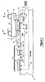
- reference numeral 11 identifies an electronic device which is to be tested while its temperature is maintained near a constant set point.
- Two specific examples of this electronic device 11 are an integrated chip which is packaged in ceramic or plastic, or a bare chip which is unpackaged.
- Any type of circuitry which needs to be tested can be integrated into the electronic device 11, such as digital logic circuitry or memory circuitry or analog circuitry; and that circuitry can be comprised of any type of transistors, such as N-channel field effect transistors or P-channel field effect transistors or complimentary field effect transistors or bi-polar transistors.
- TEMP output signals
- All of the remaining components 12-17 in Fig. 1 constitute a temperature control system which keeps the temperature of the electronic device 11 near the set point while that device is being tested.
- Each component in this control system is described below in TABLE 1.
- TABLE 1 COMPONENT DESCRIPTION 12 ...
- Component 12 is a printed circuit board which physically holds the components 11, 16, 17 and 18. Also, the printed circuit board 12 contains several sets of signal and power lines 12a-12g. 13 .
- Component 13 is a thin, flat electric heater which has two major faces 13a and 13b that lie against components 11 and 14 respectively. A variable amount of electrical power P h is supplied to the heater 13 via two wires 13c, and that power is dissipated as heat within the heater.
- One embodiment of the heater 13 is comprised of aluminum nitride ceramic in which electrical resistors (not shown) are uniformly integrated for converting the power from the conductors 13c to heat.
- Component 14 is a liquid cooled heat sink that has a hollow base 14a in which cooling fins (not shown) are disposed.
- a liquid coolant 14b enters the base 14a from a tube 14c, and that liquid coolant exits the base via another tube 14d.
- This coolant 14b is circulated through the base 14a at a constant flow rate by a pump (not shown) and held at a constant temperature T L ⁇ 15 .
- Component 15 is an electronic control circuit which sends the variable amount of electrical power P h to the electric heater 13.
- This control circuit 15 consists of a power regulator 16 and a variable power supply 17.
- 16 ... Component 16 is a power regulator which is coupled to three sets of signal lines 12c, 12d, and 12e. the TEMP signals which indicate the present temperature T d of the electronic device 11 are received on the signal lines 12c, and SET- POINT signals which indicate the set point temperature for the device 11 are received on the signal lines 12d. Based on those two temperatures and their rate of change, power regulator 16 generates control signals CTL on the signal lines 12e which indicate the amount of power that should be sent to the heater 13 such that the temperature of the device 11 stays near the set point. 17 ... Component 17 is a variable power supply which is coupled to the signal lines 12e and two sets of power lines 12f and 12g.
- the control signals CTL from the power regulator 16 are received, and on the power lines 12f, a supply voltage +V and ground are received.
- the power supply 17 sends the variable amount of power P h on the power lines 12g as a portion of the power which is available from the supply voltage +V.
- Component 18 is a connector which intercouples the heater wires 13c to the variable power supply.
- the electronic device 11 In operation, the electronic device 11 varies in its power dissipation as it is being tested by the TEST-IN signals which it receives on the signal lines 12a. This variation in power occurs because the transistors in the electronic device 11 turn on and off, and thereby vary in their power dissipation, in response to the TEST-IN signals. Consequently, the temperature of the electronic device 11 tends to increase as its power dissipation increases; and vice-versa.
- a temperature sensor generates the TEMP signals on the signal lines 12c which indicate the present temperature of the device. Those TEMP signals are sent to the power regulator 16 where they are compared with the SET-POINT signals on the signal lines 12d. If the temperature of the device 11 is less than the set point temperature, then the regulator 16 generates the control signals CTL such that the variable power P h to the heater 13 is increased. Conversely, if the temperature of the device 11 is more than the set point temperature, then the regulator 16 generates the control signals CTL such that the variable power PWR to the heater 13 is decreased.
- FIG. 2 is schematic diagrams of the Fig. 1 control system wherein the electronic device 11 is coupled to the electric heater 13 through a thermal resistance ⁇ d-h ; the heater 13 is coupled to the heat sink base 14a through a thermal resistance ⁇ h-s ; and the heat sink base is coupled to the liquid coolant through a thermal resistance ⁇ s-L . Also in the Figs. 2-4 , the electronic device 11 receives and dissipates a variable amount of power P d , and the electric heater receives and dissipates a variable amount of power P h ⁇ Further in the
- the heater's thermal mass M h is made as small as is practical. This constraint, as will be shown below, helps to improve the speed with which the heater 13 can raise or lower its temperature, and thereby maintain the temperature T d of the electronic device near the set point.
- One suitable upper limit for the thermal mass M h is that it be no larger than three times the thermal mass M d of the electronic device; and preferably, M h is less than M d .
- the heater's thermal resistance ⁇ d-h is made as small as practical. This constraint, as will be shown below, helps to increase the amount of heat that is transferred from the heater 13 to the electronic device 11, relative to the amount of heat that is transferred from the heater 13 to the heat sink 14.
- a suitable upper limit for the thermal resistance ⁇ d-h is that it be no more than three times the thermal resistance ⁇ h-s between the heater and the heat sink base; and preferably, ⁇ d-h is less than ⁇ h-s .
- the electronic device 11 increases its power dissipation P d and thereby causes its temperature T d to rise above the set point. This is shown in Fig. 3 as occurring at time instants t1 and t2.
- the power P h to the heater 13 is reduced by the regulator 16; and this is shown in Fig. 3 as occurring at time t3.
- Heater 13 has a low thermal mass M h ; and consequently, the heater's temperature T h drops rapidly when the heater's power is reduced, as indicated at time t4.
- the heater temperature T d starts to cool down, as indicated at time t5.
- the heater power P h ramps up as indicated at time t6.
- the heater temperature T h rises and thereby reduces the flow of heat from the device 11 along the thermal path 21.
- the electronic device 11 decreases its power dissipation P d and thereby causes its temperature T d to drop below the set point. This is shown in Fig. 4 as occurring at time instants t1 and t2.
- the power P h to the heater 13 is increased by the regulator 16; and this is shown in Fig. 4 as occurring at time t3.
- Heater 13 has a low thermal mass M h ; and consequently, the heater's temperature T h rises rapidly when the heater's power is increased as indicated at time t4.
- the heater temperature T h rises so high that it exceeds the device temperature T d , one portion of the heat from the heater travels along the thermal path 22a in Fig. 4 to the electronic device 11, and another portion of the heat from the heater travels along the thermal path 22b to the liquid coolant. Also, the amount of heat which travels on path 22a to the electronic device 11 increases as ⁇ d-h decreases relative to ⁇ h-s .
- the device temperature T d starts to rise, as indicated at time t5.
- the heater power P h ramps down as indicated at time t6.
- the heater temperature T h ramps down and thereby reduces the flow of heat from the heater to the device 11 along the thermal path 22a.
- the heater 13 controls the amount of heat that flows on the paths 21 and 22a.
- T h equals T d
- T h is less than T d
- T h is more than T d
- Fig. 5 three differential equations are provided which are labeled equation 1, equation 2, and equation 3. These equations are based on the principle that the sum of the thermal power which is received by a body is equal to the thermal mass of the body times the rate of change of the body's temperature.
- Equation 1 contains three terms which are identified by reference numerals 31a, 31b and 31c.
- Term 31a is the power which the electronic device 11 receives and dissipates in response to the TEST-IN signals;
- term 31b is the power which is transferred to the electronic device 11 through the thermal resistance ⁇ d-h ; and
- term 31c is the thermal mass of the electronic device 11 times the rate of change of its temperature.
- equation 2 contains four terms which are identified by reference numerals 32a, 32b, 32c, and 32d.
- Term 32a is the power which is supplied to the electric heater 13 from the variable power supply 17;
- term 32b is the power which is transferred to the electric heater 13 through the thermal resistance ⁇ h-s ;
- term 32c is the power which is transferred to the heater 13 through the thermal resistance ⁇ d-h ;
- term 32d is the thermal mass of the heater times the rate of change of the heater's temperature.
- equation 3 contains three terms which are identified by reference numerals 33a, 33b, and 33c.
- Term 33a is the power which is transferred to the heat sink base 14a through the thermal resistance ⁇ S-L ;
- term 33b is the power which is transferred to the heat sink base through the thermal resistance ⁇ h-s ;
- term 33c is the mass of the heat sink base times the rate of change of its temperature.
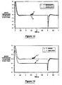
- the simulation assumed that the electronic device 11 was initially at the set point temperature and was dissipating no power. Thereafter, at a time equal to two seconds, the power dissipation of the electronic device 11 was stepped up in response to the TEST-IN signals, to a power of 100 watts. This power dissipation remained constant in the electronic device 11 for three seconds at which time the power dissipation in the device 11 went back to zero.
- the thermal mass M d in TABLE 2 is the thermal mass of a bare integrated circuit chip; and thus, it constitutes another worst case test condition because its temperature will change temperature faster than the temperature of a packaged chip (which inherently has a larger thermal mass).
- Curve 41 in Fig. 6 shows how the power dissipation in the electronic device 11 changes with time, as described above. Also in Figs. 6 and 7 , curve 42 shows how the temperature of the electronic device 11 change with time; curve 43 shows how the heater power changes with time; curve 44 shows how the heater's temperature changes with time; and curve 45 shows how the temperature of the heat sink base changes with time.
- curve 42 shows that the maximum deviation in the temperature of the electronic device 11 is approximately 3.6°C due to the negative step in power dissipation within that device. After reaching that maximum temperature deviation, the temperature of the electronic device 11 ramps up and returns to the set point within 0.3 seconds.
- each deviation in the device temperature from the set point is corrected by a change in the heater power P h as given by term 32a in equation 2.
- the temperature of the heater changes as indicated by term 32d in equation 2.
- a change in heater temperature then causes term 31b to change in equation 1.
- the change in term 31b causes the device temperature to change as indicated by term 31c in equation 1.
- Fig. 5 the above chain of events is indicated by a dashed line 51.
- Fig. 8 is a schematic diagram for the control system which occurs in Figs. 7 and 8 of the prior art patent '521.
- the reference numerals 140, 116, 124, 126, and 82 are the same reference numerals which occur in Fig. 7 of patent '521.
- Component 140 is a heater block which contacts the electronic device 11 that is to be cooled; component 116 is an aluminum block which contacts the heater block; component 82 is a coolant tube which carries a liquid coolant at a temperature T L ; component 124 is a heater assembly which contacts the aluminum block 116; and component 126 is a heating element in the heater assembly.
- Each component in Fig. 8 has a respective thermal mass M and a respective temperature T as shown in the figure. Also, all of the components in Fig. 8 are intercoupled through respective thermal resistance's ⁇ as shown.
- Fig. 9 a set of six differential equations 11-15 can be derived as shown in Fig. 9 .
- Fig. 9 equations are similar to the equations of Fig. 5 is that they are based on the principle that the sum of the thermal power which is received by a body is equal to the thermal mass of the body times the rate of change of the body's temperature.
- Fig. 9 the above chain of events is indicated by reference numeral 51'.
- each of the temperatures T 3 , T 2 , T 1 , T h , and T d must sequentially change in order to regulate the device temperature by varying the heater power P h . Consequently, varying the heater power only indirectly changes the device temperature.
- the chain of events 51 in Fig. 5 only the temperatures T h and T d must sequentially change in order to regulate the device temperature by varying the heater power. Consequently, varying the heater power in the Fig. 1 control system affects the device temperature much more directly, and thus more quickly, than it does in patent '521.
- Equation 20 is formed by adding equations 2 and 3 of Fig. 5 together, and by rearranging the resulting terms such that only term 32d lies to the left of the equal sign.
- equation 21 is obtained by adding equations 12-16 of Fig. 9 together, and by rearranging the resulting terms such that only term 67 lies to the left of the equal sign.
- the thermal mass M h is the thermal mass of the Fig. 1 heater 13 which is in direct contact with the electronic device 11 that is to be cooled.
- the thermal mass M h is the thermal mass of the Fig. 8 heater block 140 which is in direct contact with the electronic device 11 that is to be cooled.
- Term 60 in equation 21 is similar to term 33c in equation 20; and thus their negative effects on changing the temperature T h by varying the heater power P h are similar. But the remaining negative terms 61, 63, and 65 in equation 21 are completely eliminated in equation 20. Thus, changing the heater power P h has a much larger effect on the rate of change of the temperature T h in the Fig. 1 control system than it does in patent '521.
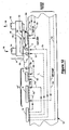
- Figs. 11 and 12 a second temperature control system will be described.
- a major point of distinction in this second temperature control system over the Fig. 1 system is that it regulates the temperature of an electronic device 11' which does not include a temperature sensor. Consequently, the electronic device 11' is unable to generate the temperature signals TEMP which indicate how its temperature is varying in response to the TEST-IN signals on the signal lines 12a.
- This distinguishing point is very significant since many, if not most, integrated circuit chips in the prior art do not include a temperature sensor.
- Equation 2 provides the principle on which this second temperature control system is based; and for convenience equation 2 is reproduced in Fig. 11 .
- equation 31 is obtained wherein the device temperature T d is expressed in terms of several parameters which are on the right of the equals sign.
- the parameters T h , ⁇ h , P h , and T s vary with time as each particular device 11' is being tested; and the remaining parameters ⁇ d-h , M h , and ⁇ h-s are essentially constant.
- the device temperature T d can be estimated by measuring the constant parameters ⁇ d-h , M h , and ⁇ h-s before the device 11' is tested and by sensing the parameters T h , ⁇ h , P h , and T s while the device 11 is tested. Then, if the estimated device temperature is above the set point, the heater temperature is decreased; and vice-versa.
- Fig. 12 shows all of the components of a temperature control system which operates on the above principle.
- the heater 13' is the same as the heater 13 of Fig. 1 , except that it includes a sensor 13d which senses the heater temperature T h .
- the heat sink 14' is the same as heat sink 14 of Fig. 1 except that it includes a sensor 14f which senses the heat sink temperature T s .
- Component 12' in Fig. 12 is the same as the printed circuit board 12 in Fig. 1 , except that it includes five different sets of signal lines 12c', 12e', 12h, 12i and 12j, plus two connectors 71 and 72.
- Signal lines 12h carry the sensed heater temperature T h ;
- signal lines 12i carry the sensed heat sink temperature T s ;
- signal lines 12j carry the measured parameters ⁇ d-h , M h , and ⁇ h-s ;
- signal lines 12e' carry the control signals CTL which indicate the heater power P h ;
- signal lines 12c' carry the estimated device temperature T d .
- Component 73 in Fig. 12 estimates the device temperature based on equation 31 and all of the parameters which it receives on the signal lines 12e', 12i, 12j and 12h.
- Component 73 can be a digital microprocessor chip which digitally calculates the device temperature from equation 31; or alternatively, component 71 can be an analog circuit which calculates the device temperature from equation 31 in an analog fashion.
- Components 16, 17 and 18 are identical to those components in Fig. 1 which have the same reference numeral. Components 16, 17 and 18 together constitute a control circuit 15' which receives an estimated device temperature on the signal lines 12c', and receives the set point temperature on the signals lines 12d. When the estimated device temperature exceeds the set point temperature, the control circuit 15' reduces the power P h to the heater 13'; and vice-versa.
- FIG. 13 A digital simulation of the Fig. 12 temperature control system is shown in Fig. 13 .
- the electronic device 11' had a step increase in power when the simulation time equaled three seconds, and it had a step decrease in power when the simulation time equaled six seconds.
- Curve 91 in Fig. 13 (which is comprised of a series of small circles), shows how the estimated device temperature varied with time during the simulation; and curve 92 in Fig. 13 , (which is a solid line), shows how the actual device temperature would be sensed if the device had a temperature sensor.
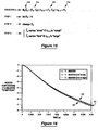
- Figs. 15 and 16 One preferred method by which the actual ⁇ d-h can be measured for each device is shown in Figs. 15 and 16 .
- This method which includes steps 1-3, is based on equation 2, which again is reproduced in Fig. 15 . If ⁇ d-h is smaller than its average value, then T d -T h will decrease. Thus term 32c will decrease, and so the rate of change of heater temperature in term 32d will decrease. Conversely, if, ⁇ d-h , is larger than its average value, then the rate of change of heater temperature in term 32d will increase.
- step 1 of the Fig. 15 process the power dissipation of the device 11' is set to zero. Then in step 2, the heater power P h is varied in some predetermined fashion. Suitably, the heater power is stepped up, or stepped down, or varied as a sine wave. Next in step 3, the effect which varying the heater power has on ⁇ h is sensed and correlated to ⁇ d-h .
- the heater temperature is sensed at some time after P h drops to zero, such as at time equal to 0.04 seconds. Then by extrapolation from the curves 93, 94 and 95, the actual ⁇ d-h is obtained.
- the typical resistivity which can be obtained between the contacting surfaces is about 1.3°C cm 2 /watt. This resistivity will be larger if the contacting surfaces are less flat. Placing a thermal pad between two non-flat surfaces reduces the resistivity between them, but a practical resistivity which an be obtained through a thermal pad is about 1.0°C cm 2 /watt. By comparison, with the method of Figs. 17-19 , the resistivity from the electronic device to the heater has been reduced to 0.07°C cm 2 /watt. This is an improvement of 1.0 ⁇ 0.07, which is more than 1000%.
- a drop of a particular type of liquid 101 is dispensed onto the surface of the electronic device 11 (or 11') which is to make contact with the heater 13 (or 13'). This step is shown in Fig. 17 .
- Two limiting characteristics of the liquid 101 are - a) that it is a good thermal conductor relative to air, and b) that it evaporates, without leaving any residue, at a temperature which is too low to damage the electronic device.
- the liquid 101 evaporates at a temperature of less than two hundred degrees centigrade.
- One preferred embodiment of the liquid 101 is water.
- a second embodiment of the liquid 101 is a mixture of water and a volatile material (e.g. ethylene glycol) which elevates the boiling point of the mixture above the boiling point of water.
- a third embodiment of the liquid 101 is a mixture of water and a volatile material (e.g. methanol) which suppresses the freezing point of the mixture below the freezing point of water.
- a fourth embodiment of the liquid 101 is a mixture of water and a volatile material (e.g. ethanol) which enhances the wetability of the mixture above the wetability of water.
- the thermal resistivity from the heater 13 (or 13') to the electronic device 11 (of 11') is substantially reduced over that which it would otherwise be without the liquid.
- the liquid 101' is water and the flatness of the mating surfaces is less than 5 ⁇ m, then the above-described resistivity of about 0.07°C cm 2 /watt is obtained.
- the pressure between it and the heater preferably is less than 10 psi.
- Fig. 18 also shows that the mating surfaces between the heater and the heat sink are not perfectly flat. But those two surfaces preferably are joined in a permanent fashion, for example by a layer 102 of thermally conductive epoxy.
- a suitable thickness for the layer 102 is 50 ⁇ m-80 ⁇ m.
- the electronic device While the electronic device and the heater and the heat sink are all coupled together as shown in Fig. 18 , the electronic device is tested and its temperature is kept near the set point by the control systems of Figs. 1 or 12 . Thereafter, when the test is complete, the electronic device is separated from the heater. Then the liquid 101' is removed from the electronic device by evaporation; and this is indicated by the arrows 103 in Fig. 19 .
- the total time which it takes to evaporate all of the liquid 101' is proportional to the area of the liquid 101' which is exposed. If the electronic device is square with a dimension L on each side, then the exposed area in Fig. 19 is L 2 . By comparison, when the electronic device is being tested in the Fig. 18 structure, the exposed area of the liquid 101' is greatly reduced to (4L)(5 ⁇ m).
- L is less than one-half inch. In that case, the liquid 101' evaporates more than 500 times slower in the Fig. 18 structure than it does in Fig. 19 . Thus, during short tests (i.e., less than one hour) no significant amount of liquid 101' will be lost from the Fig. 18 structure due to evaporation.
- One feature of the above process is that after the liquid 101' is evaporated, no residue remains on the electronic device. Consequently, the electronic device can be put into an end product without any additional clean-up steps.
- Another feature of the above process is that it is very easy and inexpensive to perform. Only one step is needed to dispense a drop of the liquid 101 on the electronic device as shown in Fig. 17 , and only one step is needed to push the heater against the electronic device as shown in Fig. 18 .
- Fig. 20 shows a modification wherein the temperature of the electronic device 11 (or 11') is kept near the set point by the use of a laser.
- This Fig. 20 modification can be incorporated into the temperature control systems of the previously described Figs. 1 , 12 , and 18 .
- reference number 13" identifies a modified electric heater; and reference number 14" identifies a modified heat sink. Included in the modified heater 13" is a laser 13a" which generates an infrared laser beam 13b" , and a thin, flat piece of infrared laser beam absorbing material 13c" . This material 13c" has two major faces 13d” and 13e” which respectively lie against the electronic component 11 (or 11') and the heat sink 14" .
- the modified heat sink 14" is the same as the previously described heat sinks of Figs. 1 or 12 , except that the base 14a" includes two windows 14e" and 14f" , and no cooling fins are disposed in the base between the windows.
- Window 14e" is transparent to the infrared laser beam 13b" and is thermally conductive.
- Window 14f" also is transparent to the laser beam 13b" , but it need not be thermally conductive.
- the windows are made of monocrystalline silicon.
- the temperature of the electronic device 11 is either sensed directly as per the Fig. 1 control system, or estimated as per the Fig. 12 control system. Then, if the device temperature T d is above the set point, the power P h to the laser on lines 13f" is reduced by the control circuit 15 of Fig. 1 , or by the control circuit 15' of Fig. 12 . Conversely if the device temperature is below the set point, the power P h to the laser is increased.
- the enhanced thermal interface of Fig. 18 can be incorporated into a temperature control system other than the one of Figs. 1 and 12 .
- An example of this modification is shown in Fig. 21 .
- the heater 13 or 13' or 13" and the corresponding circuitry for controlling the heater power P h is eliminated; and the heat sink 14 (or 14') is pressed against the electronic device with the liquid film 101' disposed there between.
- the temperature of the electronic device 11 (or 11') will vary substantially more from the set point than it does when the heater 13 ( or 13' or 13") is present. But on the other hand, the temperature of the electronic device will vary substantially less with the Fig. 21 modification than the variation which occurs if the liquid film 101' is absent. For particular tests on particular electronic devices, such as chips with a small variation in power dissipation, the amount of temperature regulation which is achieved with the Fig. 21 modification will be sufficient; and all costs associated with the heater and its control circuits are eliminated.
- the temperature control system of Fig. 1 can be changed to an open loop control system in which the electronic device 11 does not send any TEMP signals to the power regulator 16.
- the tester sequentially sends a series of predicted temperatures on the signals lines 12d to the power regulator 16 for each particular TEST-IN signal which it sends to the electronic device 11.
- the power regulator 16 compares the predicted temperature of electronic device 11 with the set point temperature. If the predicted temperature is less than the set point temperature, then the regulator 16 generates the control signals CTL such that the variable power P h to the heater 13 is increased. Conversely, if the predicted temperature is more than the set point temperature, then the regulator 16 generates the control signal CTL such that the variable power P h to the heater 13 is decreased.
- the electric heater 13" of Fig. 20 can be whanged such that the infrared laser beam absorbing material 13c" is eliminated.
- the window 14e" lies against the electronic device 11 (or 11'); and the laser beam 13b" is absorbed directly by the electronic device.
- the Fig. 1 temperature control system can be changed such that the TEMP signals on the signal lines 12c originate from a temperature sensor that is attached to the external surface of the electronic device 11. This modification is useful when a temperature sensor is not integrated into the electronic device 11.
- the Fig. 1 and Fig. 12 temperature control systems can be changed such that the set point temperature on the signal lines 12d varies with time.
- the set point temperature can be stepped from one level to another, or it can vary continuously in a ramped or sinusoidal fashion.
Abstract
Description
- This invention relates to temperature control systems which maintain the temperature of an electronic device near a constant set point temperature while the device is being tested; and it relates to subassemblies which comprise key portions of such temperature control systems.
- Two specific example of electronic devices which have a need to be tested near a constant temperature are packaged integrated chips, or bare chips which are unpackaged. Any type of circuitry can be integrated into the chips, such as digital logic circuitry or memory circuitry or analog circuitry. Also, the circuitry in the chips can be comprised of any type of transistors, such as field effect transistors or bi-polar transistors.
- One reason for trying to keep the temperature of a chip constant while it is tested is that the speed with which the chip operates may be temperature dependent. For example, a chip comprised of complementary field effect transistors (CMOS transistors) typically increases its speed of operation by about 0.3% per °C drop in chip temperature.
- A common practice in the chip industry is to mass produce a particular type of chip, and then speed sort them and sell the faster operating chips at a higher price. CMOS memory chips and CMOS microprocessor chips are processed in this fashion. However, in order to determine the speed of such chips properly, the temperature of each chip must be kept nearly constant while the speed test is performed.
- Maintaining the chip temperature near a constant set point is quite simple if the instantaneous power dissipation of the chip is constant or varies in a small range while the speed test is being performed. In that case, it is only necessary to couple the chip through a fixed thermal resistance to a thermal mass which is at a fixed temperature. For example, if the maximum chip power variation is ten watts, and the coupling between the chip and the thermal mass is 0.2°C/watt, then the chip temperature will vary a maximum of 2°C.
- But, if the instantaneous power dissipation of the chip varies up and down in a wide range while the speed test is being performed, then maintaining the chip temperature near a constant set point is very difficult. Each time the device power dissipation makes a big change, its temperature and its speed will also make a big change.
- The above problem is particularly severe in CMOS chips because their instantaneous power dissipation increases as the number of CMOS transistors which are switching ON or OFF increases. During the speed test of a CMOS chip, the number of transistors which are switching is always changing; thus, the chip's power dissipation and temperature and speed are always changing. Also, the magnitude of these changes increases as more transistors get integrated into a single chip, because the number of transistors which are switching at any particular instant will vary from none to all of the transistors on the chip.
- In the prior art, several temperature control systems for integrated circuit chips have been disclosed by the following U.S. patents:
5,420,521 5,297,621 5,104,661 5,315,240 5,205,132 5,125,656 5,309,090 5,172,049 4,734,872. - However, none of the temperature control systems which are disclosed in the above patents are capable of enabling speed tests to be run on chips which widely vary their power dissipation during the test. This is because the above temperature control systems cannot react fast enough to compensate for such instantaneous power variations.
- In the above patent '656 and '661 and '090 and 240, no means are provided for removing heat from the chip; they merely include various heaters for adding heat to the chip. These control systems are suitable only for raising the chip's temperature to an elevated level, such as above 200°C, at which "burn-in" tests are performed. At any elevated temperature, the failure of weak or faulty components in a chip is accelerated, and the "burn-in" test causes such components to fail after several hours.
- In the above patents '872 and '132 and '621, the chip temperature is increased or lowered by directing a temperature controlled gas jet at the chip or immersing the chip in a temperature controlled liquid. But, these control systems are limited by the speed at which the temperature of the gas jet or liquid can be increased or decreased.
- In patent '521, a control system is disclosed in
Fig. 7 which includes both a heater for heating the chip and a liquid cooled aluminum block for cooling the chip. However, theFig. 7 control system still is not capable of enabling speed tests to be run on chips which widely vary their power dissipation during the test, because it cannot react fast enough to compensate for such power variations. Why this deficiency occurs is explained herein in detail in conjunction withFigs. 8, 9 , and10 . - Accordingly, a primary object of the inventions which are disclosed herein is to provide novel temperature control systems, and novel subassemblies for such systems, which react quickly to large variations in power dissipation within an electronic device and thereby maintain the device temperature near a constant set point temperature while the device is being tested.
- In accordance with the invention of Docket 550,577, a temperature control system which maintains the temperature of an electronic device near a set point comprises: an electric heater that has a first face which makes contact with the electronic device, and a second face which is opposite the first face; a heat sink, coupled to the second face of the heater, which absorbs heat from the electronic device through the heater's second face; a temperature sensor, coupled to the electronic device which senses the device temperature Td; and, a control circuit, coupled to the temperature sensor and to the heater, which decreases the power to the heater when the sensed temperature of the electronic device is above the set point, and vice-versa. When the heater temperature Th is less than Td, then heat flows from the electronic device through the heater to the heat sink; and the rate of heat flow increases as Td-Th increases. When Th is more than Td, then heat flows to the electronic device from the heater; and the rate of heat flow increases as Th-Td increases. By electrically controlling just the heater power, heat flow to/from the electronic device is quickly adjusted; and that in turn quickly regulates the device temperature.
-
-
Fig. 1 shows a temperature control system which constitutes a preferred embodiment of the invention having Docket No. 550,577. -
Fig. 2 is a schematic diagram which helps explain the operation of theFig. 1 temperature control system. -
Fig. 3 replicates the schematic diagram ofFig. 2 and depicts the operation of theFig. 1 control system for the case where the power dissipation in the electronic device steps up. -
Fig. 4 replicates the schematic diagram ofFig. 2 and depicts the operation of theFig. 1 control system for the case where the power dissipation in the electronic device steps down. -
Fig. 5 is a set of differential equations which precisely defines the behavior of theFig. 1 control system. -
Fig. 6 shows how several parameters vary in theFig. 1 control system when that system is simulated via theFig. 5 equations. -
Fig. 7 shows how several additional parameters vary in theFig. 1 control system when that system is simulated via theFig. 5 equations. -
Fig. 8 is a schematic diagram, similar to the schematic diagram ofFig. 2 , which helps explain the operation of a prior art temperature control system that is described inU.S. Patent 5,420,521 . -
Fig. 9 is a set of differential equations which precisely defines the behavior of theFig. 8 temperature control system and help explain a distinguishing feature between the operation of the control systems ofFigs. 1 and8 . -
Fig. 10 is a set of differential equations which helps explain another distinguishing feature between the operation of the control systems ofFigs. 1 and8 . -
Fig. 11 is a set of differential equations which forms the basis of the temperature control system having Docket 550,578. -
Fig. 12 shows a preferred embodiment of the temperature control system which is based on theFig. 11 equations. -
Fig. 13 is a set of curves which is obtained by a simulation of theFig. 12 temperature control system. -
Fig. 14 is another set of curves which is obtained by a second simulation of theFig. 12 temperature control system in which a particular parameter is injected with an error. -
Fig. 15 lists the steps of a process by which the error in the parameter ofFig. 14 can be detected and corrected. -
Fig. 16 illustrates how theFig. 15 process is carried out. -
Fig. 17 shows an initial stage of fabricating a subassembly which constitutes the invention having Docket No. 550,579. -
Fig. 18 shows how the subassembly ofFig. 17 is completed and incorporated into the temperature control systems ofFigs. 1 and12 . -
Fig. 19 shows how a film on an electronic device in the subassembly ofFig. 18 is removed. -
Fig. 20 shows a modification for a heater component within the temperature control systems ofFigs. 1 and12 . -
Fig. 21 shows a modification for the subassembly ofFig. 18 . - In
Fig. 1 ,reference numeral 11 identifies an electronic device which is to be tested while its temperature is maintained near a constant set point. Two specific examples of thiselectronic device 11 are an integrated chip which is packaged in ceramic or plastic, or a bare chip which is unpackaged. Any type of circuitry which needs to be tested can be integrated into theelectronic device 11, such as digital logic circuitry or memory circuitry or analog circuitry; and that circuitry can be comprised of any type of transistors, such as N-channel field effect transistors or P-channel field effect transistors or complimentary field effect transistors or bi-polar transistors. - Included on the
electronic device 11 are dozens of input/output terminals 11a; but for simplicity inFig. 1 , only a few of those terminals are shown. Theseterminals 11a are coupled to three sets ofsignal lines signal lines 12a, input signals " TEST-IN" are received which test theelectronic device 11; and on thesignal lines 12b, output signals " TEST-OUT" are sent from theelectronic device 11 as a response to the test. Conventional test equipment (not shown) is coupled to thesignal lines signal lines 12c, output signals " TEMP" are sent from theelectronic device 11 which indicate its temperature. These TEMP signals originate from a temperature sensor, such as a temperature sensitive resistor or diode, which is integrated into the electronic device. - All of the remaining components 12-17 in
Fig. 1 constitute a temperature control system which keeps the temperature of theelectronic device 11 near the set point while that device is being tested. Each component in this control system is described below in TABLE 1.TABLE 1 COMPONENT DESCRIPTION 12 ... Component 12 is a printed circuit board whichphysically holds the components 18. Also, the printed circuit board 12 containsseveral sets of signal and power lines 12a-12g.13 ... Component 13 is a thin, flat electric heaterwhich has two major faces against components variable amount of electrical power Ph is supplied to the heater 13 via twowires 13c, andthat power is dissipated as heat within the heater. One embodiment of the heater 13 iscomprised of aluminum nitride ceramic in which electrical resistors (not shown) are uniformly integrated for converting the power from the conductors 13c to heat.14 ... Component 14 is a liquid cooled heat sink thathas a hollow base 14a in which cooling fins (notshown) are disposed. A liquid coolant 14b entersthe base 14a from a tube 14c, and that liquidcoolant exits the base via another tube 14d.This coolant 14b is circulated through thebase 14a at a constant flow rate by a pump (not shown) and held at a constant temperature TL· 15 ... Component 15 is an electronic control circuitwhich sends the variable amount of electrical power Ph to the electric heater 13. Thiscontrol circuit 15 consists of a power regulator 16 and avariable power supply 17.16 ... Component 16 is a power regulator which iscoupled to three sets of signal lines and 12e. the TEMP signals which indicate the present temperature Td of the electronic device 11 are received on the signal lines 12c, and SET-POINT signals which indicate the set point temperature for the device 11 are received on thesignal lines 12d. Based on those twotemperatures and their rate of change, power regulator 16 generates control signals CTL on the signal lines 12e which indicate the amount ofpower that should be sent to the heater 13 suchthat the temperature of the device 11 stays nearthe set point. 17 ... Component 17 is a variable power supply which iscoupled to the signal lines 12e and two sets ofpower lines signal lines 12e, the control signals CTL from the power regulator 16 are received, and on the power lines 12f, a supply voltage +V and ground are received. In response to the CTL signals, the power supply 17 sends the variable amount of power Ph on the power lines 12g as a portion of the power whichis available from the supply voltage +V. 18 ... Component 18 is a connector which intercouplesthe heater wires 13c to the variable powersupply. - In operation, the
electronic device 11 varies in its power dissipation as it is being tested by the TEST-IN signals which it receives on thesignal lines 12a. This variation in power occurs because the transistors in theelectronic device 11 turn on and off, and thereby vary in their power dissipation, in response to the TEST-IN signals. Consequently, the temperature of theelectronic device 11 tends to increase as its power dissipation increases; and vice-versa. - Within the
electronic device 11, a temperature sensor generates the TEMP signals on thesignal lines 12c which indicate the present temperature of the device. Those TEMP signals are sent to thepower regulator 16 where they are compared with the SET-POINT signals on thesignal lines 12d. If the temperature of thedevice 11 is less than the set point temperature, then theregulator 16 generates the control signals CTL such that the variable power Ph to theheater 13 is increased. Conversely, if the temperature of thedevice 11 is more than the set point temperature, then theregulator 16 generates the control signals CTL such that the variable power PWR to theheater 13 is decreased. - Turning now to
Figs. 2, 3 and 4 , the operation of theFig. 1 control system will be described in further detail. Those figures are schematic diagrams of theFig. 1 control system wherein theelectronic device 11 is coupled to theelectric heater 13 through a thermal resistance θd-h; theheater 13 is coupled to theheat sink base 14a through a thermal resistance θh-s; and the heat sink base is coupled to the liquid coolant through a thermal resistance θs-L. Also in theFigs. 2-4 , theelectronic device 11 receives and dissipates a variable amount of power Pd, and the electric heater receives and dissipates a variable amount of power Ph· Further in the -
Figs. 2-4 , theelectronic device 11 has a temperature Td and a thermal mass Md; theheater 13 has a temperature Th and a thermal mass Mh; and theheat sink base 14a has a temperature TS and a thermal mass MS· - Preferably, the heater's thermal mass Mh is made as small as is practical. This constraint, as will be shown below, helps to improve the speed with which the
heater 13 can raise or lower its temperature, and thereby maintain the temperature Td of the electronic device near the set point. One suitable upper limit for the thermal mass Mh is that it be no larger than three times the thermal mass Md of the electronic device; and preferably, Mh is less than Md. - Also preferably, the heater's thermal resistance θd-h is made as small as practical. This constraint, as will be shown below, helps to increase the amount of heat that is transferred from the
heater 13 to theelectronic device 11, relative to the amount of heat that is transferred from theheater 13 to theheat sink 14. A suitable upper limit for the thermal resistance θd-h is that it be no more than three times the thermal resistance θh-s between the heater and the heat sink base; and preferably, θd-h is less than θh-s. - Under steady state conditions, heat flows from the
device 11 to the liquid coolant along athermal path 21 as shown inFig. 2 , and heat flows from theheater 13 to the liquid coolant along athermal path 22 as shown inFig. 2 . Also under steady state conditions, the device temperature equals the set point temperature, and the heater temperature equals the device temperature minus Pdθd-h. If the device power dissipation is zero, then the heat flow onpath 21 is zero and Td equals Th. - Suppose now that the
electronic device 11 increases its power dissipation Pd and thereby causes its temperature Td to rise above the set point. This is shown inFig. 3 as occurring at time instants t1 and t2. In response to the rise in the device temperature Td above the set point, the power Ph to theheater 13 is reduced by theregulator 16; and this is shown inFig. 3 as occurring at time t3.Heater 13 has a low thermal mass Mh; and consequently, the heater's temperature Th drops rapidly when the heater's power is reduced, as indicated at time t4. - As the heater temperature is reduced, the amount of heat which is transferred from the
device 11 along thethermal path 21 to the liquid coolant increases. Thus, the device temperature Td starts to cool down, as indicated at time t5. As the device temperature Td approaches the set point, the heater power Ph ramps up as indicated at time t6. Thus the heater temperature Th rises and thereby reduces the flow of heat from thedevice 11 along thethermal path 21. By raising the heater power Ph to the proper level, a steady state returns where the heat flow is as shown inFig. 2 and the device temperature Td is at the set point. - Conversely, suppose that the
electronic device 11 decreases its power dissipation Pd and thereby causes its temperature Td to drop below the set point. This is shown inFig. 4 as occurring at time instants t1 and t2. In response to the drop in the device temperature Td below the set point, the power Ph to theheater 13 is increased by theregulator 16; and this is shown inFig. 4 as occurring at time t3.Heater 13 has a low thermal mass Mh ; and consequently, the heater's temperature Th rises rapidly when the heater's power is increased as indicated at time t4. - If the heater temperature Th rises so high that it exceeds the device temperature Td, one portion of the heat from the heater travels along the
thermal path 22a inFig. 4 to theelectronic device 11, and another portion of the heat from the heater travels along thethermal path 22b to the liquid coolant. Also, the amount of heat which travels onpath 22a to theelectronic device 11 increases as θd-h decreases relative to θh-s. - In response to the rise in heater temperature at time t4, the device temperature Td starts to rise, as indicated at time t5. As the device temperature Td approaches the set point, the heater power Ph ramps down as indicated at time t6. Thus the heater temperature Th ramps down and thereby reduces the flow of heat from the heater to the
device 11 along thethermal path 22a. By dropping the heater power Ph to the proper level, a steady state returns where the heat flow is as shown inFig. 2 and the device temperature Td is at the set point temperature. - From the above description of
Figs. 2-4 , it is seen that theheater 13 controls the amount of heat that flows on thepaths path path 21 from the electronic device through theheater 13 to the heat sink; and the rate of heat flow increases as Td-Th increases. When Th is more than Td, then heat flows onpath 22a from theheater 13 to the electronic device; and the rate of heat flow increases as Th-Td increases. By controlling the heater power Ph, heat flow to/from the electronic device is regulated; and that in turn regulates the device temperature. - To further explain the speed with which the
Fig. 1 control system operates, reference should now be made toFigs. 5, 6 and 7 . InFig. 5 , three differential equations are provided which are labeledequation 1,equation 2, andequation 3. These equations are based on the principle that the sum of the thermal power which is received by a body is equal to the thermal mass of the body times the rate of change of the body's temperature. -
Equation 1 contains three terms which are identified byreference numerals Term 31a is the power which theelectronic device 11 receives and dissipates in response to the TEST-IN signals;term 31b is the power which is transferred to theelectronic device 11 through the thermal resistance θd-h; andterm 31c is the thermal mass of theelectronic device 11 times the rate of change of its temperature. - Similarly,
equation 2 contains four terms which are identified byreference numerals Term 32a is the power which is supplied to theelectric heater 13 from thevariable power supply 17;term 32b is the power which is transferred to theelectric heater 13 through the thermal resistance θh-s;term 32c is the power which is transferred to theheater 13 through the thermal resistance θd-h; andterm 32d is the thermal mass of the heater times the rate of change of the heater's temperature. - Likewise,
equation 3 contains three terms which are identified byreference numerals Term 33a is the power which is transferred to theheat sink base 14a through the thermal resistance θS-L;term 33b is the power which is transferred to the heat sink base through the thermal resistance θh-s; andterm 33c is the mass of the heat sink base times the rate of change of its temperature. - Using the three equations of
Fig. 5 , a simulation on a digital computer was performed; and the results of that simulation are shown inFigs. 6 and 7 . In performing this simulation, the various parameters in theFig. 5 equations had the values which are shown below in TABLE 2.TABLE 2 θd-h= 0.1°C per watt Md = 478 joules per °C θh-s= 0.05°C per watt Mh = 0.80 joules per °C θs-L= 0.1°C per watt Ms = 5.60 joules per °C MAXIMUM Ph= 500 watts TL = 40°C below set point - Also, the simulation assumed that the
electronic device 11 was initially at the set point temperature and was dissipating no power. Thereafter, at a time equal to two seconds, the power dissipation of theelectronic device 11 was stepped up in response to the TEST-IN signals, to a power of 100 watts. This power dissipation remained constant in theelectronic device 11 for three seconds at which time the power dissipation in thedevice 11 went back to zero. - By changing the power dissipation of the
electronic device 11 with a pair of one hundred watt steps as described above, the ability of theFig. 1 control system to maintain the device temperature near the set point is tested under a worst case condition. Also, the thermal mass Md in TABLE 2 is the thermal mass of a bare integrated circuit chip; and thus, it constitutes another worst case test condition because its temperature will change temperature faster than the temperature of a packaged chip (which inherently has a larger thermal mass). -
Curve 41 inFig. 6 shows how the power dissipation in theelectronic device 11 changes with time, as described above. Also inFigs. 6 and 7 , curve 42 shows how the temperature of theelectronic device 11 change with time;curve 43 shows how the heater power changes with time;curve 44 shows how the heater's temperature changes with time; andcurve 45 shows how the temperature of the heat sink base changes with time. - Inspection of curve 42, at time equal to two seconds, shows that the maximum deviation in the temperature of the
electronic device 11 is approximately 4°C due to the step increase in power dissipation within that device. After reaching that maximum temperature deviation, the temperature of theelectronic device 11 then ramps down and returns to the set point within about 0.4 seconds. - Similarly, inspection of curve 42, at time equal to five seconds, shows that the maximum deviation in the temperature of the
electronic device 11 is approximately 3.6°C due to the negative step in power dissipation within that device. After reaching that maximum temperature deviation, the temperature of theelectronic device 11 ramps up and returns to the set point within 0.3 seconds. - One primary feature of the above-described control system is the speed with which the control system corrects a deviation in the device temperature from the set point, and thus keeps the maximum deviation relatively small. How this speed of operation is achieved can be seen from the equations in
Fig. 5 as follows. - Each deviation in the device temperature from the set point is corrected by a change in the heater power Ph as given by
term 32a inequation 2. Whenterm 32a changes, the temperature of the heater changes as indicated byterm 32d inequation 2. A change in heater temperature then causesterm 31b to change inequation 1. Then the change interm 31b causes the device temperature to change as indicated byterm 31c inequation 1. InFig. 5 , the above chain of events is indicated by a dashedline 51. - By comparison, in the prior art patent 5,420,521 the chain of events which occur between a change in the heater power and a resulting change in the device temperature is much longer; and this is shown by
Figs. 8 and 9. Fig. 8 is a schematic diagram for the control system which occurs inFigs. 7 and8 of the prior art patent '521. In this schematic diagram, thereference numerals Fig. 7 of patent '521. -
Component 140 is a heater block which contacts theelectronic device 11 that is to be cooled;component 116 is an aluminum block which contacts the heater block;component 82 is a coolant tube which carries a liquid coolant at a temperature TL;component 124 is a heater assembly which contacts thealuminum block 116; andcomponent 126 is a heating element in the heater assembly. Each component inFig. 8 has a respective thermal mass M and a respective temperature T as shown in the figure. Also, all of the components inFig. 8 are intercoupled through respective thermal resistance's θ as shown. - From the schematic diagram of
Fig. 8 , a set of six differential equations 11-15 can be derived as shown inFig. 9 . TheseFig. 9 equations are similar to the equations ofFig. 5 is that they are based on the principle that the sum of the thermal power which is received by a body is equal to the thermal mass of the body times the rate of change of the body's temperature. - When the heater power Ph in
equation 15 changes, that causes the temperature T3 to change as indicated byterm 61 inequation 15. A change in the temperature T3 then causesterm 62 to change inequation 14. Then the change interm 62 causes the temperature T2 to change as indicated byterm 63 ofequation 14. A change in the temperature T2 then causesterm 64 to changeequation 13. Then the change interm 64 causes the temperature T1 to change as indicated byterm 65 ofequation 13. A change in the temperature T1 then causesterm 66 to change inequation 12. Then the change interm 66 causes the temperature Th to change as indicated byterm 67 ofequation 12. A change in the temperature Th then causesterm 68 to change inequation 11. Then the change interm 68 causes the device temperature Td to change as indicated byterm 69 ofequation 11. - In
Fig. 9 , the above chain of events is indicated by reference numeral 51'. In this chain of events 51', each of the temperatures T3, T2, T1, Th, and Td must sequentially change in order to regulate the device temperature by varying the heater power Ph. Consequently, varying the heater power only indirectly changes the device temperature. By comparison, in the chain ofevents 51 inFig. 5 , only the temperatures Th and Td must sequentially change in order to regulate the device temperature by varying the heater power. Consequently, varying the heater power in theFig. 1 control system affects the device temperature much more directly, and thus more quickly, than it does in patent '521. - Another reason why varying the heater power in the
Fig. 1 control system effects the device temperature more quickly than it does in patent '521 can be seen fromequations Fig. 10 .Equation 20 is formed by addingequations Fig. 5 together, and by rearranging the resulting terms such thatonly term 32d lies to the left of the equal sign. Similarly,equation 21 is obtained by adding equations 12-16 ofFig. 9 together, and by rearranging the resulting terms such thatonly term 67 lies to the left of the equal sign. - In
term 32d ofequation 20, the thermal mass Mh is the thermal mass of theFig. 1 heater 13 which is in direct contact with theelectronic device 11 that is to be cooled. Similarly, interm 67 ofequation 21, the thermal mass Mh is the thermal mass of theFig. 8 heater block 140 which is in direct contact with theelectronic device 11 that is to be cooled. Thus, in order to regulate the temperature of theelectronic device 11 quickly, it is critical that the temperature Th of the mass Mh can be changed quickly by varying the heater power Ph. - When the heater power Ph increases in
equation 20, the effect of that power increase on the temperature Th of the mass Mh is diminished by thenegative term 33c which occurs in the right-hand side ofequation 20. By comparison, when the heater power Ph inequation 21 is increased, the effect of that power increase on the temperature Th of the mass Mh is diminished by fournegative terms equation 21. -
Term 60 inequation 21 is similar toterm 33c inequation 20; and thus their negative effects on changing the temperature Th by varying the heater power Ph are similar. But the remainingnegative terms equation 21 are completely eliminated inequation 20. Thus, changing the heater power Ph has a much larger effect on the rate of change of the temperature Th in theFig. 1 control system than it does in patent '521. - Turning now to
Figs. 11 and12 , a second temperature control system will be described. A major point of distinction in this second temperature control system over theFig. 1 system is that it regulates the temperature of an electronic device 11' which does not include a temperature sensor. Consequently, the electronic device 11' is unable to generate the temperature signals TEMP which indicate how its temperature is varying in response to the TEST-IN signals on thesignal lines 12a. This distinguishing point is very significant since many, if not most, integrated circuit chips in the prior art do not include a temperature sensor. -
Equation 2, as previously described, provides the principle on which this second temperature control system is based; and forconvenience equation 2 is reproduced inFig. 11 . By algebraically rearranging the terms ofequation 2, another equation 31 is obtained wherein the device temperature Td is expressed in terms of several parameters which are on the right of the equals sign. - In equation 31, the parameters Th, Ṫh, Ph, and Ts vary with time as each particular device 11' is being tested; and the remaining parameters θd-h, Mh, and θh-s are essentially constant. Thus, from equation 31, the device temperature Td can be estimated by measuring the constant parameters θd-h, Mh, and θh-s before the device 11' is tested and by sensing the parameters Th, Ṫh, Ph, and Ts while the
device 11 is tested. Then, if the estimated device temperature is above the set point, the heater temperature is decreased; and vice-versa. -
Fig. 12 shows all of the components of a temperature control system which operates on the above principle. InFig. 12 , the heater 13' is the same as theheater 13 ofFig. 1 , except that it includes asensor 13d which senses the heater temperature Th. Similarly inFig. 12 , the heat sink 14' is the same asheat sink 14 ofFig. 1 except that it includes asensor 14f which senses the heat sink temperature Ts. - Component 12' in
Fig. 12 is the same as the printedcircuit board 12 inFig. 1 , except that it includes five different sets ofsignal lines 12c', 12e', 12h, 12i and 12j, plus twoconnectors Signal lines 12h carry the sensed heater temperature Th; signal lines 12i carry the sensed heat sink temperature Ts;signal lines 12j carry the measured parameters θd-h, Mh, and θh-s;signal lines 12e' carry the control signals CTL which indicate the heater power Ph; andsignal lines 12c' carry the estimated device temperature Td. -
Component 73 inFig. 12 estimates the device temperature based on equation 31 and all of the parameters which it receives on thesignal lines 12e', 12i, 12j and 12h.Component 73 can be a digital microprocessor chip which digitally calculates the device temperature from equation 31; or alternatively,component 71 can be an analog circuit which calculates the device temperature from equation 31 in an analog fashion. -
Components Fig. 1 which have the same reference numeral.Components signal lines 12c', and receives the set point temperature on thesignals lines 12d. When the estimated device temperature exceeds the set point temperature, the control circuit 15' reduces the power Ph to the heater 13'; and vice-versa. - A digital simulation of the
Fig. 12 temperature control system is shown inFig. 13 . In this simulation, the electronic device 11' had a step increase in power when the simulation time equaled three seconds, and it had a step decrease in power when the simulation time equaled six seconds.Curve 91 inFig. 13 , (which is comprised of a series of small circles), shows how the estimated device temperature varied with time during the simulation; andcurve 92 inFig. 13 , (which is a solid line), shows how the actual device temperature would be sensed if the device had a temperature sensor. - When the above simulation of
Fig. 13 was performed, it was assumed that all of the parameters on the right-hand side of equation 31 were sensed or measured with no errors. This is a valid assumption for θh-s and Mh because they are essentially fixed and can be measured accurately. Also Th and Ts can be made as accurate as desired by using proper temperature sensors, and Ph is known from the control signal CTL. But in a mass production environment, where many electronic devices are tested one at a time, the parameter θd-h may vary within some range from an average value due to microscopic variations in physical contact between the heater 13' and each device 11'. - If an average value of θd-h is sent to the
estimator component 73, but the actual value of θd-h differs from that average value, then an error in the estimated device temperature will occur. As a result, an offset will occur between the actual temperature of the device 11' as regulated by theFig. 12 control system and the set point temperature. This is evident fromFig. 14 where a curve 91', (which is comprised of a series of small circles), shows how the estimated device temperature varies with time when the actual θd-h is 20% smaller than the average θd-h; and a curve 92', (which is a solid line), shows how the actual device temperature varied with time. - When certain types of devices 11' are tested, some offset between the actual device temperature and set point temperature may be acceptable, in which case it is sufficient to send the average value of θd-h to the
estimator 73. If, however, the amount of offset is not acceptable, then the offset can be reduced by measuring the actual θd-h for each device that is tested. - One preferred method by which the actual θd-h can be measured for each device is shown in
Figs. 15 and 16 . This method, which includes steps 1-3, is based onequation 2, which again is reproduced inFig. 15 . If θd-h is smaller than its average value, then Td-Th will decrease. Thusterm 32c will decrease, and so the rate of change of heater temperature interm 32d will decrease. Conversely, if, θd-h, is larger than its average value, then the rate of change of heater temperature interm 32d will increase. - In
step 1 of theFig. 15 process, the power dissipation of the device 11' is set to zero. Then instep 2, the heater power Ph is varied in some predetermined fashion. Suitably, the heater power is stepped up, or stepped down, or varied as a sine wave. Next instep 3, the effect which varying the heater power has on Ṫh is sensed and correlated to θd-h. - If Ṫh varies faster than average, then the actual θd-h is larger than its average value; whereas if Ṫ h varies slower than average, then θd-h is smaller than its average value. This is indicated in
Fig. 16 bycurves Curve 93 was obtained by setting θd-h equal to its average value, raising Ph to the set point and waiting until the device temperature reached the set point, and then dropping Ph to zero.Curves - To measure the actual value of θd-h for any deviation from the average, the heater temperature is sensed at some time after Ph drops to zero, such as at time equal to 0.04 seconds. Then by extrapolation from the
curves - Next, with reference to
Figs. 17-19 , a preferred process for minimizing the thermal resistance θd-h in the temperature control systems ofFigs. 1 and12 will be described. This process is significant because as θd-h is reduced, the amount of heat that can be transferred from the heater to the electronic device increases relative to the amount of heat that is transferred from the heater to the heat sink. Such heat transfers occur when the heater temperature exceeds the device temperature, was was explained previously in conjunction withFig. 4 . - If a dry contact is made between the electronic device 11 (or 11') and the heater 13 (or 13'), and the contacting surfaces are very flat (i.e., less than 5µm deviation from a perfect plane), then the typical resistivity which can be obtained between the contacting surfaces is about 1.3°C cm2/watt. This resistivity will be larger if the contacting surfaces are less flat. Placing a thermal pad between two non-flat surfaces reduces the resistivity between them, but a practical resistivity which an be obtained through a thermal pad is about 1.0°C cm2/watt. By comparison, with the method of
Figs. 17-19 , the resistivity from the electronic device to the heater has been reduced to 0.07°C cm2/watt. This is an improvement of 1.0 ÷ 0.07, which is more than 1000%. - Initially in the process of
Figs. 17-19 , a drop of a particular type ofliquid 101 is dispensed onto the surface of the electronic device 11 (or 11') which is to make contact with the heater 13 (or 13'). This step is shown inFig. 17 . Two limiting characteristics of the liquid 101 are - a) that it is a good thermal conductor relative to air, and b) that it evaporates, without leaving any residue, at a temperature which is too low to damage the electronic device. Preferably, the liquid 101 evaporates at a temperature of less than two hundred degrees centigrade. - One preferred embodiment of the liquid 101 is water. A second embodiment of the liquid 101 is a mixture of water and a volatile material (e.g. ethylene glycol) which elevates the boiling point of the mixture above the boiling point of water. A third embodiment of the liquid 101 is a mixture of water and a volatile material (e.g. methanol) which suppresses the freezing point of the mixture below the freezing point of water. A fourth embodiment of the liquid 101 is a mixture of water and a volatile material (e.g. ethanol) which enhances the wetability of the mixture above the wetability of water.
- After the liquid 101 is dispensed on the electronic device as described above,
surface 13a of the heater is pressed against that liquid. This step is shown inFig. 18 . As a result, some of the originally dispensedliquid 101 is squeezed out, and the remaining liquid 101' fills the microscopic gaps which inherently exist between the electronic device and the heater. These gaps occur becausesurface 13a of the heater and the mating surface of the electronic device are not perfectly flat. - Due to the presence of the liquid 101', the thermal resistivity from the heater 13 (or 13') to the electronic device 11 (of 11') is substantially reduced over that which it would otherwise be without the liquid. When the liquid 101' is water and the flatness of the mating surfaces is less than 5µm, then the above-described resistivity of about 0.07°C cm2/watt is obtained.
- One way to reduce the size of the gaps between the mating surfaces of the electronic device and the heater is to increase the pressure with which those two surfaces are pushed together; and this in turn will tend to decrease θd-h. But, if too much pressure is applied, the electronic device or an interconnect to it can crack. Thus, for the case where the electronic device is a bare integrated circuit die, the pressure between it and the heater preferably is less than 10 psi.
-
Fig. 18 also shows that the mating surfaces between the heater and the heat sink are not perfectly flat. But those two surfaces preferably are joined in a permanent fashion, for example by alayer 102 of thermally conductive epoxy. A suitable thickness for thelayer 102 is 50µm-80µm. - While the electronic device and the heater and the heat sink are all coupled together as shown in
Fig. 18 , the electronic device is tested and its temperature is kept near the set point by the control systems ofFigs. 1 or12 . Thereafter, when the test is complete, the electronic device is separated from the heater. Then the liquid 101' is removed from the electronic device by evaporation; and this is indicated by thearrows 103 inFig. 19 . - The total time which it takes to evaporate all of the liquid 101' is proportional to the area of the liquid 101' which is exposed. If the electronic device is square with a dimension L on each side, then the exposed area in
Fig. 19 is L2. By comparison, when the electronic device is being tested in theFig. 18 structure, the exposed area of the liquid 101' is greatly reduced to (4L)(5µm). - If the electronic device is a typical integrated circuit chip, then L is less than one-half inch. In that case, the liquid 101' evaporates more than 500 times slower in the
Fig. 18 structure than it does inFig. 19 . Thus, during short tests (i.e., less than one hour) no significant amount of liquid 101' will be lost from theFig. 18 structure due to evaporation. - One feature of the above process is that after the liquid 101' is evaporated, no residue remains on the electronic device. Consequently, the electronic device can be put into an end product without any additional clean-up steps. Another feature of the above process is that it is very easy and inexpensive to perform. Only one step is needed to dispense a drop of the liquid 101 on the electronic device as shown in
Fig. 17 , and only one step is needed to push the heater against the electronic device as shown inFig. 18 . - Three separate, but related, inventions have now been described in detail in conjunction with
Figs. 1-10 ,Figs. 11-16 , andFigs. 17-19 respectively. In addition, various changes and modifications can be made to the details of these Figs. without departing from the nature and spirit of the inventions. - For example,
Fig. 20 shows a modification wherein the temperature of the electronic device 11 (or 11') is kept near the set point by the use of a laser. ThisFig. 20 modification can be incorporated into the temperature control systems of the previously describedFigs. 1 ,12 , and18 . - In
Fig. 20 ,reference number 13" identifies a modified electric heater; andreference number 14" identifies a modified heat sink. Included in the modifiedheater 13" is alaser 13a" which generates aninfrared laser beam 13b" , and a thin, flat piece of infrared laserbeam absorbing material 13c" . This material 13c" has twomajor faces 13d" and 13e" which respectively lie against the electronic component 11 (or 11') and theheat sink 14" . - The modified
heat sink 14" is the same as the previously described heat sinks ofFigs. 1 or12 , except that thebase 14a" includes twowindows 14e" and 14f" , and no cooling fins are disposed in the base between the windows.Window 14e" is transparent to theinfrared laser beam 13b" and is thermally conductive.Window 14f" also is transparent to thelaser beam 13b" , but it need not be thermally conductive. Suitably, the windows are made of monocrystalline silicon. - In operation, the temperature of the electronic device 11 (or 11') is either sensed directly as per the
Fig. 1 control system, or estimated as per theFig. 12 control system. Then, if the device temperature Td is above the set point, the power Ph to the laser onlines 13f" is reduced by thecontrol circuit 15 ofFig. 1 , or by the control circuit 15' ofFig. 12 . Conversely if the device temperature is below the set point, the power Ph to the laser is increased. - As another modification, the enhanced thermal interface of
Fig. 18 can be incorporated into a temperature control system other than the one ofFigs. 1 and12 . An example of this modification is shown inFig. 21 . In theFig. 1 control system the heater 13 (or 13' or 13") and the corresponding circuitry for controlling the heater power Ph is eliminated; and the heat sink 14 (or 14') is pressed against the electronic device with the liquid film 101' disposed there between. - With the
Fig. 21 modification, the temperature of the electronic device 11 (or 11') will vary substantially more from the set point than it does when the heater 13 ( or 13' or 13") is present. But on the other hand, the temperature of the electronic device will vary substantially less with theFig. 21 modification than the variation which occurs if the liquid film 101' is absent. For particular tests on particular electronic devices, such as chips with a small variation in power dissipation, the amount of temperature regulation which is achieved with theFig. 21 modification will be sufficient; and all costs associated with the heater and its control circuits are eliminated. - As another modification, the temperature control system of
Fig. 1 can be changed to an open loop control system in which theelectronic device 11 does not send any TEMP signals to thepower regulator 16. With this modification, the tester sequentially sends a series of predicted temperatures on the signals lines 12d to thepower regulator 16 for each particular TEST-IN signal which it sends to theelectronic device 11. In response, thepower regulator 16 compares the predicted temperature ofelectronic device 11 with the set point temperature. If the predicted temperature is less than the set point temperature, then theregulator 16 generates the control signals CTL such that the variable power Ph to theheater 13 is increased. Conversely, if the predicted temperature is more than the set point temperature, then theregulator 16 generates the control signal CTL such that the variable power Ph to theheater 13 is decreased. - As still another modification, the
electric heater 13" ofFig. 20 can be whanged such that the infrared laserbeam absorbing material 13c" is eliminated. With this modification, thewindow 14e" lies against the electronic device 11 (or 11'); and thelaser beam 13b" is absorbed directly by the electronic device. - As another modification, the
Fig. 1 temperature control system can be changed such that the TEMP signals on thesignal lines 12c originate from a temperature sensor that is attached to the external surface of theelectronic device 11. This modification is useful when a temperature sensor is not integrated into theelectronic device 11. - As another modification, the
Fig. 1 andFig. 12 temperature control systems can be changed such that the set point temperature on thesignal lines 12d varies with time. For example, the set point temperature can be stepped from one level to another, or it can vary continuously in a ramped or sinusoidal fashion. - Accordingly, it is to be understood that the present inventions are not limited to the details of any one embodiment in any one figure, but are defined by the appended claims.
Claims (16)
- A temperature control system which maintains the temperature of an electronic device near a set point temperature and including:an electric heater (13) that has a first face (13a) for making contact with said electronic device (11), a second face (13b) which is opposite said first face (13a), a heat sink (14) which is coupled to said second face (13b) of said heater (13) such that said heater (13) is interposed between said heat sink (14) and said electronic device (11); andmeans for determining the temperature of the electronic device (11), preferably implemented as a temperature sensor (12c),further characterized by a control circuit (15), coupled to said means for determining the temperature of the electronic device and to said heater (13), which decreases the power to said heater (13) when the temperature of said electronic device (11) is above said set point, and vice-versa.
- The temperature control system according to claim 1, wherein said heater (13) includes electric resistors between or on said first and second face (13a, 13b).
- The temperature control system according to claim 1, wherein said heater (13) includes a laser absorbing material between or on said first and second face (13a, 13b).
- The temperature control system according to claim 3, wherein said means for determining the temperature of the electronic device includes a temperature sensor (12c) integrated into said electronic device (11).
- The temperature control system according to claim 1, wherein the means for determining the temperature of the electronic device is a temperature sensor (13d) attached to the exterior of said electronic device (11).
- The temperature control system according to one or more of claims 1-5, wherein said heater (13) includes electric resistors between or on said first and second face (13a, 13b), and wherein said control circuit (15) sends current to said resistors.
- The temperature control system according to one or more of claims 1-5, wherein said heater (13) includes a laser absorbing material between or on said first and second face (13a, 13b), and wherein said control circuit (15) heats said material with a laser.
- The temperature control system according to one or more of claims 1-7, wherein each face (13a, 13b) of said heater (13) has a certain length, and wherein said heater (13) is thin in extent from said first face (13a) to said second face (13b) in comparison to that length.
- The temperature control system according to one or more of claims 1-7, wherein said heater (13) is flat and less than one-quarter centimeter thick.
- The temperature control system according to one or more of claims 1-9, wherein the thermal mass of said heater (13) is no more than three times the thermal mass of said electronic device (11).
- The temperature control system according to one or more of claims 1-10, wherein the thermal mass of said heater (13) is less than the thermal mass of said electronic device (11).
- The temperature control system according to one or more of claims 1-11, wherein the thermal resistance from said heater (13) to said electronic device (11) is less than three times the thermal resistance from said heater (13) to said heat sink (14).
- The temperature control system according to one or more of claims 1-11, wherein the thermal resistance from said heater (13) to said electronic device (11) is less than the thermal resistance from said heater (13) to said heat sink (14).
- The temperature control system according to one or more of claims 1-13, wherein the power dissipation of said electronic device (11) is varied by sending input signals to said electronic device (11) which switch transistors ON and OFF in said electronic device (11) and simultaneously test said electronic device (11).
- The temperature control system according to one or more of claims 1-14, wherein lying between said first face (13a) of said heater (13) and said electronic device (11) is a film of a liquid which evaporates, without leaving any residue, at a temperature that is too low to damage the electronic device (11).
- The temperature control system according to one or more of claims 1-15, wherein due to said heater (13) being interposed between said electronic device (11) and said heat sink (14), the heat generated by said electronic device (11) flows by thermal conduction through said heater (13) to said heat sink (14) when the temperature of said electronic device (11) is at a set point under steady state conditions.
Applications Claiming Priority (4)
| Application Number | Priority Date | Filing Date | Title |
|---|---|---|---|
| US08/833,369 US5821505A (en) | 1997-04-04 | 1997-04-04 | Temperature control system for an electronic device which achieves a quick response by interposing a heater between the device and a heat sink |
| US08/833,273 US5864176A (en) | 1997-04-04 | 1997-04-04 | Electro-mechnical subassembly having a greatly reduced thermal resistance between two mating faces by including a film of liquid, that evaporates without leaving any residue, between the faces |
| US08/833,368 US5844208A (en) | 1997-04-04 | 1997-04-04 | Temperature control system for an electronic device in which device temperature is estimated from heater temperature and heat sink temperature |
| EP98918008A EP1016337B1 (en) | 1997-04-04 | 1998-04-03 | Temperature control system for an electronic device |
Related Parent Applications (3)
| Application Number | Title | Priority Date | Filing Date |
|---|---|---|---|
| EP98918008 Previously-Filed-Application | 1998-04-03 | ||
| EP98918008A Division EP1016337B1 (en) | 1997-04-04 | 1998-04-03 | Temperature control system for an electronic device |
| EP98918008.8 Division | 1998-10-15 |
Publications (2)
| Publication Number | Publication Date |
|---|---|
| EP2086306A1 true EP2086306A1 (en) | 2009-08-05 |
| EP2086306B1 EP2086306B1 (en) | 2013-06-05 |
Family
ID=27420238
Family Applications (4)
| Application Number | Title | Priority Date | Filing Date |
|---|---|---|---|
| EP08156473.4A Expired - Lifetime EP2086306B1 (en) | 1997-04-04 | 1998-04-03 | Temperature control system for an electronic device |
| EP98918008A Expired - Lifetime EP1016337B1 (en) | 1997-04-04 | 1998-04-03 | Temperature control system for an electronic device |
| EP99124051A Expired - Lifetime EP0993243B1 (en) | 1997-04-04 | 1998-04-03 | Method and system for thermal coupling an electronic device to a heat exchange member |
| EP99124050A Expired - Lifetime EP0994645B1 (en) | 1997-04-04 | 1998-04-03 | Temperature control system for an electronic device in which device temperature is estimated from heater temperature and heat sink temperature |
Family Applications After (3)
| Application Number | Title | Priority Date | Filing Date |
|---|---|---|---|
| EP98918008A Expired - Lifetime EP1016337B1 (en) | 1997-04-04 | 1998-04-03 | Temperature control system for an electronic device |
| EP99124051A Expired - Lifetime EP0993243B1 (en) | 1997-04-04 | 1998-04-03 | Method and system for thermal coupling an electronic device to a heat exchange member |
| EP99124050A Expired - Lifetime EP0994645B1 (en) | 1997-04-04 | 1998-04-03 | Temperature control system for an electronic device in which device temperature is estimated from heater temperature and heat sink temperature |
Country Status (4)
| Country | Link |
|---|---|
| EP (4) | EP2086306B1 (en) |
| JP (3) | JP4077523B2 (en) |
| DE (3) | DE69818468T2 (en) |
| WO (1) | WO1998046059A1 (en) |
Cited By (1)
| Publication number | Priority date | Publication date | Assignee | Title |
|---|---|---|---|---|
| GB2612169A (en) * | 2021-08-27 | 2023-04-26 | Ametek Inc | Temperature dependent electronic component heating system |
Families Citing this family (16)
| Publication number | Priority date | Publication date | Assignee | Title |
|---|---|---|---|---|
| US6668570B2 (en) | 2001-05-31 | 2003-12-30 | Kryotech, Inc. | Apparatus and method for controlling the temperature of an electronic device under test |
| US6658736B1 (en) * | 2002-08-09 | 2003-12-09 | Unisys Corporation | Method of fabricating a heat exchanger, for regulating the temperature of multiple integrated circuit modules, having a face of a solid malleable metal coated with a release agent |
| US6975028B1 (en) | 2003-03-19 | 2005-12-13 | Delta Design, Inc. | Thermal apparatus for engaging electronic device |
| US6995980B2 (en) * | 2003-08-21 | 2006-02-07 | Unisys Corporation | Temperature control system which sprays liquid coolant droplets against an IC-module and directs radiation against the IC-module |
| US7199597B2 (en) * | 2004-02-16 | 2007-04-03 | Delta Design, Inc. | Dual feedback control system for maintaining the temperature of an IC-chip near a set-point |
| DE102004042075A1 (en) * | 2004-08-31 | 2005-10-20 | Infineon Technologies Ag | Electronic circuit structure to act as a semiconductor/chip component has an electronic circuit unit, an energy supply unit and communications bus |
| DE102005001163B3 (en) * | 2005-01-10 | 2006-05-18 | Erich Reitinger | Semiconductor wafers` testing method, involves testing wafer by probes, and reducing heating energy with constant cooling efficiency, under consideration of detected increase of temperature of fluids flowing via tempered chuck device |
| JP4418772B2 (en) * | 2005-04-28 | 2010-02-24 | 富士通マイクロエレクトロニクス株式会社 | Temperature control device |
| JP4315141B2 (en) | 2005-09-09 | 2009-08-19 | セイコーエプソン株式会社 | Electronic component temperature control device and handler device |
| JP5552452B2 (en) * | 2011-03-04 | 2014-07-16 | パナソニック株式会社 | Heating / cooling test method and heating / cooling test apparatus |
| WO2013076006A1 (en) | 2011-11-24 | 2013-05-30 | Wintershall Holding GmbH | Derivatives of tris(2-hydroxyphenyl)methanes, the production thereof and use thereof for oil production |
| GB2507732A (en) * | 2012-11-07 | 2014-05-14 | Oclaro Technology Ltd | Laser temperature control |
| DE102013010088A1 (en) | 2013-06-18 | 2014-12-18 | VENSYS Elektrotechnik GmbH | Cooling device for a power converter module |
| WO2017015052A1 (en) * | 2015-07-21 | 2017-01-26 | Delta Design, Inc. | Continuous fluidic thermal interface material dispensing |
| KR200494784Y1 (en) * | 2018-11-06 | 2021-12-28 | 김진국 | Bidet |
| CN113412031A (en) * | 2021-06-21 | 2021-09-17 | 合肥联宝信息技术有限公司 | Heating module and electronic equipment |
Citations (5)
| Publication number | Priority date | Publication date | Assignee | Title |
|---|---|---|---|---|
| US3979671A (en) * | 1975-03-06 | 1976-09-07 | International Business Machines Corporation | Test fixture for use in a high speed electronic semiconductor chip test system |
| EP0314481A1 (en) * | 1987-10-28 | 1989-05-03 | Irish Transformers Limited | A temperature control instrument for electronic components under test |
| US4848090A (en) * | 1988-01-27 | 1989-07-18 | Texas Instruments Incorporated | Apparatus for controlling the temperature of an integrated circuit package |
| JPH0762424A (en) * | 1993-08-26 | 1995-03-07 | Mitsubishi Motors Corp | Laser absorber for laser hardening |
| US5420521A (en) | 1992-10-27 | 1995-05-30 | Ej Systems, Inc. | Burn-in module |
Family Cites Families (14)
| Publication number | Priority date | Publication date | Assignee | Title |
|---|---|---|---|---|
| JPS5961027A (en) * | 1982-09-29 | 1984-04-07 | Toshiba Corp | Semiconductor substrate heating apparatus |
| JPS5986235A (en) * | 1982-11-09 | 1984-05-18 | Shimada Phys & Chem Ind Co Ltd | Method for measuring electric characteristics of semiconductor device |
| US4567505A (en) * | 1983-10-27 | 1986-01-28 | The Board Of Trustees Of The Leland Stanford Junior University | Heat sink and method of attaching heat sink to a semiconductor integrated circuit and the like |
| US4854726A (en) * | 1986-05-29 | 1989-08-08 | Hughes Aircraft Company | Thermal stress screening system |
| JPH07105422B2 (en) * | 1987-03-16 | 1995-11-13 | 東京エレクトロン株式会社 | Semiconductor wafer mounting table |
| JPH01152639A (en) * | 1987-12-10 | 1989-06-15 | Canon Inc | Chuck |
| US4962416A (en) * | 1988-04-18 | 1990-10-09 | International Business Machines Corporation | Electronic package with a device positioned above a substrate by suction force between the device and heat sink |
| US4975766A (en) * | 1988-08-26 | 1990-12-04 | Nec Corporation | Structure for temperature detection in a package |
| US4975803A (en) * | 1988-12-07 | 1990-12-04 | Sundstrand Corporation | Cold plane system for cooling electronic circuit components |
| JP3201868B2 (en) * | 1992-03-20 | 2001-08-27 | アジレント・テクノロジーズ・インク | Conductive thermal interface and method |
| JPH05267200A (en) * | 1992-03-24 | 1993-10-15 | Hitachi Ltd | Semiconductor thermal treatment device |
| US5448147A (en) * | 1992-05-08 | 1995-09-05 | Tel-Varian Limited | Selectable feedback control system |
| JPH08286551A (en) * | 1995-04-12 | 1996-11-01 | Ricoh Co Ltd | Temperature controller |
| GB9610663D0 (en) * | 1996-05-22 | 1996-07-31 | Univ Paisley | Temperature control apparatus and methods |
-
1998
- 1998-04-03 DE DE69818468T patent/DE69818468T2/en not_active Expired - Lifetime
- 1998-04-03 DE DE69839520T patent/DE69839520D1/en not_active Expired - Lifetime
- 1998-04-03 EP EP08156473.4A patent/EP2086306B1/en not_active Expired - Lifetime
- 1998-04-03 DE DE69822158T patent/DE69822158T2/en not_active Expired - Lifetime
- 1998-04-03 WO PCT/US1998/006701 patent/WO1998046059A1/en active Application Filing
- 1998-04-03 EP EP98918008A patent/EP1016337B1/en not_active Expired - Lifetime
- 1998-04-03 EP EP99124051A patent/EP0993243B1/en not_active Expired - Lifetime
- 1998-04-03 JP JP54295898A patent/JP4077523B2/en not_active Expired - Lifetime
- 1998-04-03 EP EP99124050A patent/EP0994645B1/en not_active Expired - Lifetime
-
2005
- 2005-03-10 JP JP2005066502A patent/JP4122009B2/en not_active Expired - Fee Related
-
2007
- 2007-11-21 JP JP2007301819A patent/JP2008118149A/en active Pending
Patent Citations (5)
| Publication number | Priority date | Publication date | Assignee | Title |
|---|---|---|---|---|
| US3979671A (en) * | 1975-03-06 | 1976-09-07 | International Business Machines Corporation | Test fixture for use in a high speed electronic semiconductor chip test system |
| EP0314481A1 (en) * | 1987-10-28 | 1989-05-03 | Irish Transformers Limited | A temperature control instrument for electronic components under test |
| US4848090A (en) * | 1988-01-27 | 1989-07-18 | Texas Instruments Incorporated | Apparatus for controlling the temperature of an integrated circuit package |
| US5420521A (en) | 1992-10-27 | 1995-05-30 | Ej Systems, Inc. | Burn-in module |
| JPH0762424A (en) * | 1993-08-26 | 1995-03-07 | Mitsubishi Motors Corp | Laser absorber for laser hardening |
Cited By (2)
| Publication number | Priority date | Publication date | Assignee | Title |
|---|---|---|---|---|
| GB2612169A (en) * | 2021-08-27 | 2023-04-26 | Ametek Inc | Temperature dependent electronic component heating system |
| GB2612169B (en) * | 2021-08-27 | 2023-11-29 | Ametek Inc | Temperature dependent electronic component heating system |
Also Published As
| Publication number | Publication date |
|---|---|
| EP0994645A3 (en) | 2000-07-12 |
| EP0994645B1 (en) | 2003-09-24 |
| DE69818468T2 (en) | 2004-07-22 |
| EP0993243A3 (en) | 2000-07-12 |
| JP2005249798A (en) | 2005-09-15 |
| DE69839520D1 (en) | 2008-07-03 |
| EP0993243A2 (en) | 2000-04-12 |
| DE69822158T2 (en) | 2005-02-17 |
| EP0994645A2 (en) | 2000-04-19 |
| EP1016337B1 (en) | 2008-05-21 |
| JP4077523B2 (en) | 2008-04-16 |
| EP0993243B1 (en) | 2004-03-03 |
| DE69822158D1 (en) | 2004-04-08 |
| WO1998046059A1 (en) | 1998-10-15 |
| DE69818468D1 (en) | 2003-10-30 |
| JP2001526837A (en) | 2001-12-18 |
| EP2086306B1 (en) | 2013-06-05 |
| EP1016337A1 (en) | 2000-07-05 |
| JP4122009B2 (en) | 2008-07-23 |
| JP2008118149A (en) | 2008-05-22 |
Similar Documents
| Publication | Publication Date | Title |
|---|---|---|
| US5821505A (en) | Temperature control system for an electronic device which achieves a quick response by interposing a heater between the device and a heat sink | |
| US5844208A (en) | Temperature control system for an electronic device in which device temperature is estimated from heater temperature and heat sink temperature | |
| US5918665A (en) | Method of thermal coupling an electronic device to a heat exchange member while said electronic device is being tested | |
| EP1016337B1 (en) | Temperature control system for an electronic device | |
| US4402185A (en) | Thermoelectric (peltier effect) hot/cold socket for packaged I.C. microprobing | |
| US6389225B1 (en) | Apparatus, method and system of liquid-based, wide range, fast response temperature control of electronic device | |
| US5931580A (en) | Apparatus for measuring junction temperature | |
| US7394271B2 (en) | Temperature sensing and prediction in IC sockets | |
| US5260668A (en) | Semiconductor surface resistivity probe with semiconductor temperature control | |
| US8847222B2 (en) | Semiconductor device test structures and methods | |
| WO1986007192A1 (en) | Integrated semiconductor circuit and method for producing it, and use of such a circuit for providing a flow meter | |
| JPS6322623B2 (en) | ||
| US20050168212A1 (en) | Optical testing of integrated circuits with temperature control | |
| Zommer et al. | Reliability and thermal impedance studies in soft soldered power transistors | |
| Alli et al. | Thermal characteristics of plastic small outline transistor (SOT) packages | |
| Berger et al. | Reliability phenomena in aluminum metalizations on silicon dioxide | |
| JP2005127729A (en) | Reliability testing device and reliability test method | |
| O'Mathuna et al. | Test chips, test systems, and thermal test data for multichip modules in the ESPRIT-APACHIP project | |
| Wu et al. | Effects of substrate thermal characteristics on the electromigration behavior of Al thin film conductors | |
| Baderna et al. | Thermal regulator for IC temperature characterization using a microprobe station | |
| JPH04144248A (en) | Testing method of semiconductor integrated circuit | |
| Walker et al. | An infrared scanning technique for the determination of temperature profiles in microcircuits | |
| Tustaniwskyj et al. | High performance active temperature control of a device under test (DUT) | |
| JPH05243432A (en) | Semiconductor device | |
| Wesling | Thermal characterization of a 149-lead VLSI package with heatsink |
Legal Events
| Date | Code | Title | Description |
|---|---|---|---|
| PUAI | Public reference made under article 153(3) epc to a published international application that has entered the european phase |
Free format text: ORIGINAL CODE: 0009012 |
|
| AC | Divisional application: reference to earlier application |
Ref document number: 1016337 Country of ref document: EP Kind code of ref document: P |
|
| AK | Designated contracting states |
Kind code of ref document: A1 Designated state(s): DE FR GB |
|
| 17P | Request for examination filed |
Effective date: 20100126 |
|
| 17Q | First examination report despatched |
Effective date: 20100223 |
|
| AKX | Designation fees paid |
Designated state(s): DE FR GB |
|
| REG | Reference to a national code |
Ref country code: DE Ref legal event code: R079 Ref document number: 69843039 Country of ref document: DE Free format text: PREVIOUS MAIN CLASS: H05K0007200000 Ipc: G05D0023190000 |
|
| GRAP | Despatch of communication of intention to grant a patent |
Free format text: ORIGINAL CODE: EPIDOSNIGR1 |
|
| RIC1 | Information provided on ipc code assigned before grant |
Ipc: G01R 31/28 20060101ALI20121010BHEP Ipc: H01L 23/42 20060101ALI20121010BHEP Ipc: H01L 23/373 20060101ALI20121010BHEP Ipc: G05D 23/19 20060101AFI20121010BHEP Ipc: H01L 23/34 20060101ALI20121010BHEP |
|
| GRAS | Grant fee paid |
Free format text: ORIGINAL CODE: EPIDOSNIGR3 |
|
| GRAA | (expected) grant |
Free format text: ORIGINAL CODE: 0009210 |
|
| AC | Divisional application: reference to earlier application |
Ref document number: 1016337 Country of ref document: EP Kind code of ref document: P |
|
| AK | Designated contracting states |
Kind code of ref document: B1 Designated state(s): DE FR GB |
|
| REG | Reference to a national code |
Ref country code: GB Ref legal event code: FG4D |
|
| REG | Reference to a national code |
Ref country code: DE Ref legal event code: R096 Ref document number: 69843039 Country of ref document: DE Effective date: 20130801 |
|
| PLBE | No opposition filed within time limit |
Free format text: ORIGINAL CODE: 0009261 |
|
| STAA | Information on the status of an ep patent application or granted ep patent |
Free format text: STATUS: NO OPPOSITION FILED WITHIN TIME LIMIT |
|
| 26N | No opposition filed |
Effective date: 20140306 |
|
| REG | Reference to a national code |
Ref country code: DE Ref legal event code: R097 Ref document number: 69843039 Country of ref document: DE Effective date: 20140306 |
|
| GBPC | Gb: european patent ceased through non-payment of renewal fee |
Effective date: 20140403 |
|
| REG | Reference to a national code |
Ref country code: FR Ref legal event code: ST Effective date: 20141231 |
|
| PG25 | Lapsed in a contracting state [announced via postgrant information from national office to epo] |
Ref country code: GB Free format text: LAPSE BECAUSE OF NON-PAYMENT OF DUE FEES Effective date: 20140403 |
|
| PG25 | Lapsed in a contracting state [announced via postgrant information from national office to epo] |
Ref country code: FR Free format text: LAPSE BECAUSE OF NON-PAYMENT OF DUE FEES Effective date: 20140430 |
|
| PGFP | Annual fee paid to national office [announced via postgrant information from national office to epo] |
Ref country code: DE Payment date: 20160421 Year of fee payment: 19 |
|
| REG | Reference to a national code |
Ref country code: DE Ref legal event code: R119 Ref document number: 69843039 Country of ref document: DE |
|
| PG25 | Lapsed in a contracting state [announced via postgrant information from national office to epo] |
Ref country code: DE Free format text: LAPSE BECAUSE OF NON-PAYMENT OF DUE FEES Effective date: 20171103 |