EP2079107A1 - Verfahren zum herstellen eines kartenförmigen datenträgers un datenträger hergestellt nach diesem verfahren - Google Patents
Verfahren zum herstellen eines kartenförmigen datenträgers un datenträger hergestellt nach diesem verfahren Download PDFInfo
- Publication number
- EP2079107A1 EP2079107A1 EP08405006A EP08405006A EP2079107A1 EP 2079107 A1 EP2079107 A1 EP 2079107A1 EP 08405006 A EP08405006 A EP 08405006A EP 08405006 A EP08405006 A EP 08405006A EP 2079107 A1 EP2079107 A1 EP 2079107A1
- Authority
- EP
- European Patent Office
- Prior art keywords
- module
- recess
- data carrier
- card
- film
- Prior art date
- Legal status (The legal status is an assumption and is not a legal conclusion. Google has not performed a legal analysis and makes no representation as to the accuracy of the status listed.)
- Granted
Links
Images
Classifications
-
- H—ELECTRICITY
- H10—SEMICONDUCTOR DEVICES; ELECTRIC SOLID-STATE DEVICES NOT OTHERWISE PROVIDED FOR
- H10W—GENERIC PACKAGES, INTERCONNECTIONS, CONNECTORS OR OTHER CONSTRUCTIONAL DETAILS OF DEVICES COVERED BY CLASS H10
- H10W70/00—Package substrates; Interposers; Redistribution layers [RDL]
- H10W70/60—Insulating or insulated package substrates; Interposers; Redistribution layers
- H10W70/699—Insulating or insulated package substrates; Interposers; Redistribution layers for flat cards, e.g. credit cards
-
- G—PHYSICS
- G06—COMPUTING OR CALCULATING; COUNTING
- G06K—GRAPHICAL DATA READING; PRESENTATION OF DATA; RECORD CARRIERS; HANDLING RECORD CARRIERS
- G06K19/00—Record carriers for use with machines and with at least a part designed to carry digital markings
- G06K19/06—Record carriers for use with machines and with at least a part designed to carry digital markings characterised by the kind of the digital marking, e.g. shape, nature, code
- G06K19/067—Record carriers with conductive marks, printed circuits or semiconductor circuit elements, e.g. credit or identity cards also with resonating or responding marks without active components
- G06K19/07—Record carriers with conductive marks, printed circuits or semiconductor circuit elements, e.g. credit or identity cards also with resonating or responding marks without active components with integrated circuit chips
- G06K19/077—Constructional details, e.g. mounting of circuits in the carrier
- G06K19/07745—Mounting details of integrated circuit chips
Definitions
- the invention relates to a method for producing a card-shaped data carrier, using a semi-finished product having at least one film made of plastic, having a recess and an electronic module arranged in this recess, wherein the recess is made so that after insertion of the Module remains in the recess between the periphery of the module and the recess a gap.
- the invention also relates to a card-shaped data carrier which was produced by this method.
- card-shaped data carriers for example credit cards, loyalty cards, access cards or ID cards, for example, for passport control
- the module inserted into the recess is, for example, a chip module which has module connections for electrical contact with an antenna which is located in the card body.
- antennas are known per se and can be printed, etched, wound or laid, for example. As a rule, this antenna is located between two foils or layers of the card body.
- the module can have a circuit which is designed as an RFID transponder and enables non-contact detection. In principle, however, other modules and in particular electronic modules are also conceivable here.
- a film is provided with a recess in which it is punched out, for example.
- the implant is used with a suitable device and electrically connected to the antenna.
- the module is attached, for example, with a suitable adhesive in the recess.
- the recess must have a certain tolerance to the module. This tolerance has the consequence that the module used between this and the edge of the recess is a gap-shaped gap.
- a gap is disadvantageous because it can cause unacceptable flow in the later card production in the print layout.
- such a gap or gap may also cause a deformation in the card body.
- the invention has for its object to provide a method of the type mentioned, which avoids the disadvantages mentioned.
- the object is achieved in a generic method in that after inserting the module into the recess at least one film is heated and compacted locally around the module, so that the film fills the gap.
- Such heating and compacting can be carried out much easier and faster than the mentioned preparation of a prelaminate or filling with a paste.
- this heating and compacting can take place immediately after the production of the antenna in an in-line production.
- the inventive method can thus be carried out substantially as efficiently and inexpensively as a method in which said gap is not eliminated.
- a significant advantage of the inventive method is seen in the fact that the external format remains stable. The hitherto necessary subsequent trimming is therefore not required.
- Another advantage is that welded sets such as pre-laminates can be processed very easily, because the module is embedded and the trimmings are held together due to compaction.
- the method is particularly cost-effective if the heating and compression of the film takes place with a stamp which forms a welding tool.
- This welding tool is designed in particular as a sonotrode and thus heats the film by means of ultrasound. Experiments have shown that the quality is particularly high with the use of ultrasound and the film can also be heated and compacted very quickly.
- the module is inserted into at least two adjacent foil.
- Each of these films has a corresponding recess for the module.
- two films are punched out and after inserting the module, an upper and a lower film is also applied to these two films. Subsequently, it is heated and compacted around the module so that the space or gap closes around the module. As mentioned, it is heated and compacted only around the module.
- no distortion in the printed image can be recognized in the area of the chip module.
- the inventive card-shaped data carrier is characterized in that the card body is compressed inside the module around. In this card-shaped data carrier thus there is no gap between the circumference of the module and the card body.
- a film may be welded to the module at its periphery.
- such a data carrier is multi-layered.
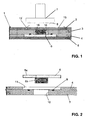
- FIG. 1 shows a portion of a card-shaped semi-finished product 1, which has a card body 15, in which an electronic module 6 is implanted.
- Such semi-finished products 1 are also called “inlets” or “inlays”.
- This module 6 is usually but not mandatory as per FIG. 2 formed from a plate-shaped support 6a and a head 6b.
- the module 6 is in particular a chip module. During implantation, this module 6 is electrically connected to an antenna 9.
- the module 6, for example, with a liquid adhesive, a hot melt adhesive (hot melt) or an adhesive film in the card body 15 is attached.
- the module 6 is inserted into a first compensating foil 3 and a second compensating foil 4.
- the first compensating film 3 has a recess 10, which is for example a rectangular or round punched-out, which receives the head 6b of the module 6.
- the second compensating film 4 has a larger recess 11 corresponding to the plate-shaped carrier 6a.
- the recess 10 is dimensioned so that after insertion of the module 6 between this and the first compensating film 3, a gap-shaped gap 16 is present, as in FIG. 1 is shown. Such a gap may also be present in the recess 11.
- the thickness of the module 6 corresponds to the sum of the two thicknesses of the compensation films 3 and 4.
- the module 6 becomes, as in FIG. 2 shown inserted into the recesses 10 and 11. Subsequently, a lower film 5 is positioned on the second compensating film 4 and an upper film 2 is positioned on the compensating film, so that finally the arrangement according to FIG FIG. 1 is present.
- a sonotrode 7 is now according FIG. 1 the card body 15 in Area of the module 6 is heated and compressed. The area corresponds essentially to that of a flat front side 8 of the sonotrode 7. The sonotrode 7 is placed with the front side 8 on a surface 12 of the card body 15. The ultrasound energy introduced into the card body 15 heats and compacts the card body around the module 6.
- a suitable vibration frequency is preferably in the range of 20-40 kHz.
- the heated card body 15 is thereby flowable and thereby closes the gap-shaped intermediate space 16. Since the volume of the intermediate space 6 is comparatively small, the other deformations on the card body 15 are very small. After this process step, the gap 16 is thus no longer present. It is essential that this heating and compression by means of the sonotrode 7 can be done very quickly.
- the usual fully automatic inline process for producing a data carrier 18 is thereby not or only slightly slowed down.
- the heating and compression by means of said sonotrode 7 is just one example. Also conceivable is heating and compression with a heating element or with hot air.
- the card body 15 shown consists of several layers 2-5. But it can also consist of only one layer. In particular, the topmost film 2 is not mandatory. This can therefore be omitted.
- the card body 15 and thus the films 2, 3, 4 and 5 are each made of a suitable plastic, in particular a thermoplastic material, as is customary in such data carriers 18.
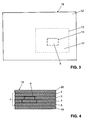
- FIG. 4 shows a section through a portion of the data carrier 18, which was prepared by laminating the semi-finished product 1 with the films 19 and 20. It will be clear to those skilled in the art that laminating may be effected with still further films not shown here, which may be printed, transparent or opaque.
- FIG. 3 shows a plan view of the disk 18.
- the implanted module 6 is shown here with dashed lines 14 and the inside of the card body condensed area 17 with dotted lines 13.
- the compacted region 17 is thus rectangular and surrounds the chip 6 in the shape of a frame.
- this area 17 can also be be a little bit bigger or smaller.
- it is in any case a partial area of the entire surface 12 of the data carrier 18.
- the area 17 could, of course, also have a different shape; it could also be, for example, circular or oval.
Landscapes
- Engineering & Computer Science (AREA)
- Computer Hardware Design (AREA)
- Microelectronics & Electronic Packaging (AREA)
- Physics & Mathematics (AREA)
- General Physics & Mathematics (AREA)
- Theoretical Computer Science (AREA)
- Credit Cards Or The Like (AREA)
Abstract
Description
- Die Erfindung betrifft ein Verfahren zum Herstellen eines kartenförmigen Datenträgers, unter Verwendung eines Halbfabrikats, das wenigstens eine aus Kunststoff hergestellte Folie besitzt, die eine Ausnehmung und ein in dieser Ausnehmung angeordnetes elektronisches Modul aufweist, wobei die Ausnehmung so hergestellt wird, dass nach dem Einsetzen des Moduls in die Ausnehmung zwischen dem Umfang des Moduls und der Ausnehmung ein Zwischenraum verbleibt. Die Erfindung betrifft zudem einen kartenförmigen Datenträger der nach diesem Verfahren hergestellt wurde.
- Verfahren zum Herstellen von kartenförmigen Datenträgern mit eingebautem Modul sind aus der
DE 102 57 111 A und derWO 2005/063909 bekannt geworden. Mit diesem Verfahren können kartenförmige Datenträger, beispielsweise Kreditkarten, Kundenkarten, Zutrittskarten oder auch Ausweise beispielsweise für die Passkontrolle hergestellt werden. Das in die Ausnehmung eingesetzte Modul ist beispielsweise ein Chip-Modul, das Modulanschlüsse für den elektrischen Kontakt zu einer Antenne besitzt, welche sich im Kartenkörper befindet. Solche Antennen sind an sich bekannt und können beispielsweise gedruckt, geätzt, gewickelt oder gelegt sein. In der Regel befindet sich diese Antenne zwischen zwei Folien oder Schichten des Kartenkörpers. Das Modul kann beispielsweise einen Schaltkreis aufweisen, der als RFID-Transponder ausgebildet ist und eine berührungslose Erkennung ermöglicht. Grundsätzlich sind hier aber auch andere Module und insbesondere elektronische Module denkbar. - Damit das Modul in den Kartenkörper implantiert werden kann, wird eine Folie mit einer Ausnehmung versehen, in dem diese beispielsweise ausgestanzt wird. In diese Ausnehmung bzw. Ausstanzung wird das Implantat mit einer geeigneten Vorrichtung eingesetzt und elektrisch mit der Antenne verbunden. Zudem wird das Modul beispielsweise mit einem geeigneten Kleber in der Ausnehmung befestigt. Damit dieses Einsetzen oder Implantieren einfach und sicher erfolgen kann, muss die Ausnehmung eine bestimmte Toleranz zum Modul aufweisen. Diese Toleranz hat zur Folge, dass beim eingesetzten Modul zwischen diesem und dem Rand der Ausnehmung ein spaltförmiger Zwischenraum besteht. Ein solcher Zwischenraum ist jedoch nachteilig, da er bei der späteren Kartenherstellung im Drucklayout ein nicht akzeptables Verfliessen verursachen kann. Zudem kann ein solcher Zwischenraum bzw. Spalt auch eine Deformation im Kartenkörper verursachen. Um diese Nachteile zu vermeiden, ist ein Verfahren bekannt geworden, bei dem der Spalt mit einer geeigneten Paste gefüllt wird. Nach einem anderen Verfahren wird ein Halbfabrikat bzw. Inlet hergestellt, das nach dem Einsetzen des Moduls mit weiteren Folien laminiert wird. Beide Verfahren bedingen aber vergleichsweise aufwändige weitere Schritte zum Herstellen eines kartenförmigen Datenträgers der genannten Art.
- Der Erfindung liegt die Aufgabe zugrunde, ein Verfahren der genannten Art zu schaffen, das die erwähnten Nachteile vermeidet. Die Aufgabe ist bei einem gattungsgemässen Verfahren dadurch gelöst, dass nach dem Einsetzen des Moduls in die Ausnehmung wenigstens eine Folie lokal um das Modul herum erwärmt und verdichtet wird, so dass die Folie den Zwischenraum füllt. Ein solches Erwärmen und Verdichten kann wesentlich einfacher und schneller durchgeführt werden als das erwähnte Herstellen eines Vorlaminates oder das Verfüllen mit einer Paste. Insbesondere kann dieses Erwärmen und Verdichten unmittelbar nach der Herstellung der Antenne bei einer Inlineproduktion erfolgen. Das erfindungsgemässe Verfahren kann somit im wesentlichen ebenso effizient und kostengünstig durchgeführt werden wie ein Verfahren, bei dem der genannte Zwischenraum nicht eliminiert wird. Ein wesentlicher Vorteil des erfindungsgemässen Verfahrens wird darin gesehen, dass das Aussenformat stabil bleibt. Das bisher notwenige nachträgliche Beschneiden ist deshalb nicht erforderlich. Vorteilhaft ist zudem, dass geschweisste Garnituren wie Vorlaminate sehr einfach weiterverarbeitet werden können, da das Modul eingebettet ist und die Garnituren aufgrund der Verdichtung zusammengehalten werden.
- Das Verfahren ist dann besonders kostengünstig, wenn das Erwärmen und Verdichten der Folie mit einem Stempel erfolgt, der ein Schweisswerkzeug bildet. Dieses Schweisswerkzeug ist insbesondere als Sonotrode ausgebildet und erwärmt somit die Folie mittels Ultraschall. Versuche haben gezeigt, dass mit der Verwendung von Ultraschall die Qualität besonders hoch ist und die Folie zudem sehr schnell erwärmt und verdichtet werden kann.
- Vorzugsweise wird nach einer Weiterbildung der Erfindung das Modul in wenigstens zwei aneinander anliegende Folie eingesetzt. Jede dieser Folie besitzt eine entsprechende Ausnehmung für das Modul. Nach einer Weiterbildung der Erfindung werden zwei Folien ausgestanzt und nach dem Einlegen des Moduls wird zudem eine obere und eine untere Folie an diese beiden Folien angelegt. Anschliessend wird um das Modul herum erwärmt und verdichtet, so dass sich der Zwischenraum bzw. der Spalt um das Modul herum schliesst. Wie erwähnt wird lediglich um das Modul herum erwärmt und verdichtet. Bei der Herstellung des Datenträgers ist dann im Bereich des Chipmoduls kein Verzug im Druckbild zu erkennen.
- Der erfindungsgemässe kartenförmige Datenträger ist dadurch gekennzeichnet, dass der Kartenkörper im Inneren um das Modul herum verdichtet ist. Bei diesem kartenförmigen Datenträger besteht somit kein Zwischenraum zwischen dem Umfang des Moduls und dem Kartenkörper. Bei einem solchen Datenträger kann eine Folie mit dem Modul an seinem Umfang verschweisst sein. Vorzugsweise ist ein solcher Datenträger mehrschichtig.
- Weitere Merkmale und Vorteile ergeben sich aus den abhängigen Patentansprüchen, der nachfolgenden Beschreibung sowie der Zeichnungen.
- Ausführungsbeispiele der Erfindung werden nachfolgend anhand der Zeichnung näher erläutert. Es zeigen:
- Figur 1
- schematisch ein Schnitt durch einen Teil eines kartenförmigen Halbfabrikat für einen Datenträger sowie ein Werkzeug zum Erwärmen und Verdichten des Kartenkörpers lokal um ein eingesetztes Modul herum,
- Figur 2
- schematisch das Einsetzen eines Moduls in ein Halbfabrikat und
- Figur 3
- schematisch eine Draufsicht auf das Halbfabrikat.
- Figur 4
- schematisch ein Schnitt durch einen Teil eines erfindungsgemässen Datenträgers.
- Die
Figur 1 zeigt einen Abschnitt eines kartenförmigen Halbfabrikat 1, der einen Kartenkörper 15 aufweist, in den ein elektronisches Modul 6 implantiert ist. Solche Halbfabrikate 1 werden auch "Inlets" oder "Inlays" genannt. Dieses Modul 6 ist üblicherweise aber nicht zwingend wie gemässFigur 2 aus einem plattenförmigen Träger 6a und einem Kopf 6b ausgebildet. Das Modul 6 ist insbesondere ein Chip-Modul. Beim Implantieren wird dieses Modul 6 mit einer Antenne 9 elektrisch verbunden. Zudem wird das Modul 6 beispielsweise mit einem Flüssigkleber, einem Heisskleber (Hotmelt) oder einer Klebefolie im Kartenkörper 15 befestigt. - Beim gezeigten Halbfabrikat 1 ist das Modul 6 in eine erste Ausgleichsfolie 3 und eine zweite Ausgleichsfolie 4 eingesetzt. Die erste Ausgleichsfolie 3 besitzt eine Ausnehmung 10, die beispielsweise eine rechteckige oder runde Ausstanzung ist, welche den Kopf 6b des Moduls 6 aufnimmt. Die zweite Ausgleichsfolie 4 besitzt eine grössere Ausnehmung 11 entsprechend dem plattenförmigen Träger 6a. Die Ausnehmung 10 ist so dimensioniert, dass nach dem Einsetzen des Moduls 6 zwischen diesem und der ersten Ausgleichsfolie 3 ein spaltförmiger Zwischenraum 16 vorhanden ist, wie dies in
Figur 1 gezeigt ist. Ein solcher Spalt kann auch in der Ausnehmung 11 vorhanden sein. Die Dicke des Moduls 6 entspricht der Summe der beiden Dicken der Ausgleichsfolien 3 und 4. - Das Modul 6 wird, wie in
Figur 2 gezeigt in die Ausnehmungen 10 und 11 eingesetzt. Anschliessend wird an der zweiten Ausgleichsfolie 4 eine untere Folie 5 und an der Ausgleichsfolie eine obere Folie 2 positioniert, so dass schliesslich die Anordnung gemässFigur 1 vorliegt. Mit einer Sonotrode 7 wird nun gemässFigur 1 der Kartenkörper 15 im Bereich des Moduls 6 erwärmt und verdichtet. Der Bereich entspricht im wesentlichen demjenigen einer ebenen Frontseite 8 der Sonotrode 7. Die Sonotrode 7 wird mit der Frontseite 8 an eine Fläche 12 des Kartenkörpers 15 angelegt. Durch die in den Kartenkörper 15 eingeleitete Ultraschallenergie wird der Kartenkörper um das Modul 6 herum erwärmt und verdichtet. Eine geeignete Schwingungsfrequenz liegt vorzugsweise im Bereich von 20 - 40 kHz. Der erwärmte Kartenkörper 15 wird dadurch fliessfähig und schliesst dadurch den spaltförmigen Zwischenraum 16. Da das Volumen des Zwischenraumes 6 vergleichsweise klein ist, sind die übrigen Deformationen am Kartenkörper 15 sehr gering. Nach diesem Verfahrensschritt ist der Zwischenraum 16 somit nicht mehr vorhanden. Wesentlich ist, dass dieses Erwärmen und Verdichten mittels der Sonotrode 7 sehr schnell erfolgen kann. Der übliche vollautomatische Inlineprozess zum Herstellen eines Datenträgers 18 wird dadurch nicht oder nur unwesentlich verlangsamt. Das Erwärmen und Verdichten mittels der genannten Sonotrode 7 ist lediglich ein Beispiel. Denkbar ist auch ein Erwärmen und Verdichten mit einem Heizelement oder mit heisser Luft. - Der gezeigte Kartenkörper 15 besteht aus mehreren Schichten 2-5. Er kann aber auch aus lediglich einer Schicht bestehen. Insbesondere ist die oberste Folie 2 nicht zwingend. Diese kann somit auch weggelassen werden.
- Der Kartenkörper 15 und somit die Folien 2, 3, 4 und 5 bestehen jeweils aus einem geeigneten Kunststoff, insbesondere einem thermoplastischen Kunststoff, wie dies bei solchen Datenträgern 18 üblich ist.
- Ist das Halbfabrikat 1 mit dem Kartenkörper 15 hergestellt, so wird dieses beispielsweise mit zwei Folien 19 und 20 laminiert. Die
Figur 4 zeigt einen Schnitt durch einen Teil des Datenträgers 18, der durch Laminieren des Halbfabrikats 1 mit den Folien 19 und 20 hergestellt wurde. Für den Fachmann ist klar, dass mit noch weiteren hier nicht gezeigten Folien laminiert werden kann, wobei diese bedruckt, transparent oder opak sein können. - Die
Figur 3 zeigt eine Draufsicht auf den Datenträger 18. Das implantierte Modul 6 ist hier mit gestrichelten Linien 14 und der im Inneren des Kartenkörpers verdichtete Bereich 17 mit punktierten Linien 13 dargestellt. Der verdichtete Bereich 17 ist hier somit rechteckig und umgibt den Chip 6 rahmenförmig. Dieser Bereich 17 kann selbstverständlich auch etwas grösser oder kleiner sein. Er ist aber jedenfalls ein Teilbereich der gesamten Fläche 12 des Datenträgers 18. Der Bereich 17 könnte selbstverständlich auch eine andere Form aufweisen, er könnte beispielsweise auch kreisrund oder oval sein. -
- 1
- Halbfabrikat
- 2
- Obere Folie
- 3
- erste Ausgleichsfolie
- 4
- zweite Ausgleichsfolie
- 5
- untere Folie
- 6
- Modul
- 6a
- Träger
- 6b
- Kopf
- 7
- Sonotrode
- 8
- Frontseite
- 9
- Antenne
- 10
- Ausnehmung
- 11
- Ausnehmung
- 12
- Fläche
- 13
- Linie
- 14
- Linie
- 15
- Kartenkörper
- 16
- Zwischenraum
- 17
- Bereich
- 18
- Datenträger
- 19
- Folie
- 20
- Folie
Claims (8)
- Verfahren zum Herstellen eines kartenförmigen Datenträgers unter Verwendung eines Halbfabrikats, das wenigstens eine aus Kunststoff hergestellte Folie (3, 4) besitzt, die eine Ausnehmung (10, 11) und ein in dieser Ausnehmung (10, 11) angeordnetes elektronisches Modul (6) aufweist, wobei die Ausnehmung (10, 11) so hergestellt wird, dass nach dem Einsetzen des Moduls (6) in die Ausnehmung (10, 11) zwischen dem Umfang des Moduls (6) und der Ausnehmung (10, 11) ein Zwischenraum (16) verbleibt, dadurch gekennzeichnet, dass nach dem Einsetzen des Moduls (6) in die Ausnehmung (10, 11) die wenigstens eine Folie (3, 4) lokal um das Modul (6) herum erwärmt und verdichtet wird, so dass die wenigstens eine Folie (3, 4) den Zwischenraum (16) schliesst.
- Verfahren nach Anspruch 1, dadurch gekennzeichnet, dass die wenigstens eine Folie (3, 5) mittels eines Stempels (7) erwärmt wird.
- Verfahren nach Anspruch 1 oder 2, dadurch gekennzeichnet, dass die wenigstens eine Folie (3, 4) mittels Ultraschall erwärmt wird.
- Verfahren nach einem der Ansprüche 1 bis 3, dadurch gekennzeichnet, dass das Modul (6) in wenigstens zwei Folien (3, 4) eingesetzt wird, die jeweils eine Ausnehmung (10, 11) für das Modul (6) aufweisen.
- Verfahren nach einem der Ansprüche 1 bis 4, dadurch gekennzeichnet, dass nach dem Einsetzen des Moduls (6) an der wenigstens einen Folie (3, 4) wenigstens eine weitere Folie (2) und insbesondere zwei weitere Folien (2, 5) positioniert wird bzw. werden.
- Kartenförmiger Datenträger mit einem Kartenkörper (15) und einem in diesen implantieren Modul (6) hergestellt nach einem der Ansprüche 1 bis 5, dadurch gekennzeichnet, dass der Kartenkörper (15) im Inneren um das Modul (6) verdichtet ist.
- Kartenförmiger Datenträger nach Anspruch 6, dadurch gekennzeichnet, dass das Modul in zwei miteinander verbundenen Folien (3, 4) eingesetzt ist.
- Kartenförmiger Datenträger nach Anspruch 6, dadurch gekennzeichnet, dass er mehrschichtig ist und dass das Modul (6) von wenigstens einer Folie (2) abgedeckt ist.
Priority Applications (4)
| Application Number | Priority Date | Filing Date | Title |
|---|---|---|---|
| EP08405006.1A EP2079107B1 (de) | 2008-01-10 | 2008-01-10 | Verfahren zum Herstellen eines kartenförmigen Datenträgers und nach diesem Verfahren hergestellter Datenträger |
| MYPI20085362A MY165396A (en) | 2008-01-10 | 2008-12-30 | Method for producing a card-type data carrier, and data carrier produced according to this method |
| BRPI0900165-4A BRPI0900165A2 (pt) | 2008-01-10 | 2009-01-06 | método para produzir um portador de dados de tipo cartão e portador de dados do tipo cartão |
| US12/319,532 US8146828B2 (en) | 2008-01-10 | 2009-01-08 | Method for producing a card-type data carrier, and data carrier produced according to this method |
Applications Claiming Priority (1)
| Application Number | Priority Date | Filing Date | Title |
|---|---|---|---|
| EP08405006.1A EP2079107B1 (de) | 2008-01-10 | 2008-01-10 | Verfahren zum Herstellen eines kartenförmigen Datenträgers und nach diesem Verfahren hergestellter Datenträger |
Publications (2)
| Publication Number | Publication Date |
|---|---|
| EP2079107A1 true EP2079107A1 (de) | 2009-07-15 |
| EP2079107B1 EP2079107B1 (de) | 2017-10-18 |
Family
ID=39345118
Family Applications (1)
| Application Number | Title | Priority Date | Filing Date |
|---|---|---|---|
| EP08405006.1A Active EP2079107B1 (de) | 2008-01-10 | 2008-01-10 | Verfahren zum Herstellen eines kartenförmigen Datenträgers und nach diesem Verfahren hergestellter Datenträger |
Country Status (4)
| Country | Link |
|---|---|
| US (1) | US8146828B2 (de) |
| EP (1) | EP2079107B1 (de) |
| BR (1) | BRPI0900165A2 (de) |
| MY (1) | MY165396A (de) |
Cited By (3)
| Publication number | Priority date | Publication date | Assignee | Title |
|---|---|---|---|---|
| WO2014161889A1 (de) * | 2013-04-05 | 2014-10-09 | Bundesdruckerei Gmbh | Wert- oder sicherheitsprodukt, verfahren zur herstellung des wert- oder sicherheitsproduktes sowie kontaktlose datenübertragungseinrichtung |
| DE102017100719A1 (de) | 2016-08-22 | 2018-02-22 | Ulrich Lang | Verfahren zum Herstellen eines Prelaminats und Fertigungsanlage |
| DE102019104380A1 (de) * | 2019-02-21 | 2020-08-27 | Bundesdruckerei Gmbh | Verfahren zur Herstellung eines Wert- oder Sicherheitsdokumentes sowie Sicherheitsdokument mit einem Sicherheitshologramm |
Families Citing this family (1)
| Publication number | Priority date | Publication date | Assignee | Title |
|---|---|---|---|---|
| US11132592B1 (en) * | 2020-05-01 | 2021-09-28 | Capital One Services, Llc | Transaction card including replaceable chip insert |
Citations (4)
| Publication number | Priority date | Publication date | Assignee | Title |
|---|---|---|---|---|
| DE3248385A1 (de) * | 1982-12-28 | 1984-06-28 | GAO Gesellschaft für Automation und Organisation mbH, 8000 München | Ausweiskarte mit integriertem schaltkreis |
| JPH11175682A (ja) | 1997-12-12 | 1999-07-02 | Hitachi Maxell Ltd | Icカード及びその製造方法 |
| DE10257111A1 (de) | 2002-12-05 | 2004-07-01 | Mühlbauer Ag | Chipkarte und Verfahren zur Herstellung einer Chipkarte |
| WO2005063909A1 (de) | 2003-12-23 | 2005-07-14 | Tesa Ag | Klebfolie zur implantierung von elektrischen modulen in einen kartenkörper |
Family Cites Families (10)
| Publication number | Priority date | Publication date | Assignee | Title |
|---|---|---|---|---|
| DE19528730A1 (de) * | 1995-08-04 | 1997-02-06 | Giesecke & Devrient Gmbh | Verfahren zur Herstellung eines Datenträgers |
| DE19731737A1 (de) * | 1997-07-23 | 1998-09-17 | Siemens Ag | Chipmodul für einen kartenförmigen Datenträger, entsprechender Kartenkörper sowie Verfahren zur Befestigung des Chipmoduls im Kartenkörper |
| GB2371264A (en) * | 2001-01-18 | 2002-07-24 | Pioneer Oriental Engineering L | Smart card with embedded antenna |
| FI111039B (fi) * | 2001-04-06 | 2003-05-15 | Rafsec Oy | Älykorttiraina ja menetelmä sen valmistamiseksi |
| AU2003223130A1 (en) * | 2002-09-03 | 2004-03-29 | 3B System, Inc. | Combination-type ic card and method of manufacturing the combination-type ic card |
| FR2881252A1 (fr) * | 2005-01-24 | 2006-07-28 | Ask Sa | Dispositif d'idenfication radiofrequence resistant aux milieux et son procede de fabrication |
| US7777317B2 (en) * | 2005-12-20 | 2010-08-17 | Assa Abloy Identification Technologies Austria GmbH (Austria) | Card and manufacturing method |
| DE102006008435A1 (de) * | 2006-02-23 | 2007-09-06 | Köra-Packmat Maschinenbau GmbH | Träger und Verfahren zur Aufnahme einer Materialschicht |
| US7707706B2 (en) * | 2007-06-29 | 2010-05-04 | Ruhlamat Gmbh | Method and arrangement for producing a smart card |
| EP2034429A1 (de) * | 2007-09-05 | 2009-03-11 | Assa Abloy AB | Herstellungsverfahren für eine Karte und mit diesem Verfahren hergestellte Karte |
-
2008
- 2008-01-10 EP EP08405006.1A patent/EP2079107B1/de active Active
- 2008-12-30 MY MYPI20085362A patent/MY165396A/en unknown
-
2009
- 2009-01-06 BR BRPI0900165-4A patent/BRPI0900165A2/pt not_active IP Right Cessation
- 2009-01-08 US US12/319,532 patent/US8146828B2/en active Active
Patent Citations (4)
| Publication number | Priority date | Publication date | Assignee | Title |
|---|---|---|---|---|
| DE3248385A1 (de) * | 1982-12-28 | 1984-06-28 | GAO Gesellschaft für Automation und Organisation mbH, 8000 München | Ausweiskarte mit integriertem schaltkreis |
| JPH11175682A (ja) | 1997-12-12 | 1999-07-02 | Hitachi Maxell Ltd | Icカード及びその製造方法 |
| DE10257111A1 (de) | 2002-12-05 | 2004-07-01 | Mühlbauer Ag | Chipkarte und Verfahren zur Herstellung einer Chipkarte |
| WO2005063909A1 (de) | 2003-12-23 | 2005-07-14 | Tesa Ag | Klebfolie zur implantierung von elektrischen modulen in einen kartenkörper |
Cited By (4)
| Publication number | Priority date | Publication date | Assignee | Title |
|---|---|---|---|---|
| WO2014161889A1 (de) * | 2013-04-05 | 2014-10-09 | Bundesdruckerei Gmbh | Wert- oder sicherheitsprodukt, verfahren zur herstellung des wert- oder sicherheitsproduktes sowie kontaktlose datenübertragungseinrichtung |
| DE102013206094B4 (de) | 2013-04-05 | 2019-03-14 | Bundesdruckerei Gmbh | Wert- oder Sicherheitsprodukt, Verfahren zur Herstellung des Wert- oder Sicherheitsproduktes sowie kontaktlose Datenübertragungseinrichtung |
| DE102017100719A1 (de) | 2016-08-22 | 2018-02-22 | Ulrich Lang | Verfahren zum Herstellen eines Prelaminats und Fertigungsanlage |
| DE102019104380A1 (de) * | 2019-02-21 | 2020-08-27 | Bundesdruckerei Gmbh | Verfahren zur Herstellung eines Wert- oder Sicherheitsdokumentes sowie Sicherheitsdokument mit einem Sicherheitshologramm |
Also Published As
| Publication number | Publication date |
|---|---|
| MY165396A (en) | 2018-03-21 |
| US20090194597A1 (en) | 2009-08-06 |
| BRPI0900165A2 (pt) | 2009-09-01 |
| EP2079107B1 (de) | 2017-10-18 |
| US8146828B2 (en) | 2012-04-03 |
Similar Documents
| Publication | Publication Date | Title |
|---|---|---|
| EP1718476B1 (de) | Verfahren zur herstellung eines buchartigen wertdokumentes sowie ein buchartiges wertdokument | |
| DE10338444B4 (de) | Transponderinlay für ein Dokument zur Personenidentifikation sowie Verfahren zu dessen Herstellung | |
| DE69929981T2 (de) | Verfahren zum herstellen einer kontaktlosen chipkarte | |
| WO2009127395A1 (de) | Chipkarte und verfahren zu deren herstellung | |
| DE102004008841A1 (de) | Verfahren zur Herstellung einer Buchdeckeneinlage und eines buchartigen Wertdokuments sowie eine Buchdeckeneinlage und ein buchartiges Wertdokument | |
| EP2079107B1 (de) | Verfahren zum Herstellen eines kartenförmigen Datenträgers und nach diesem Verfahren hergestellter Datenträger | |
| EP2936397B1 (de) | Verfahren zur herstellung eines inlays sowie inlay für einen folienverbund für ein wert- oder sicherheitsdokument | |
| WO2004080726A2 (de) | Verfahren zur herstellung einer buchdeckeneinlage und eines buchartigen wertdokumentes sowie eine buchdeckeneinlage und ein buchartiges wertdokument | |
| DE102004004469A1 (de) | Verfahren zur Herstellung eines Sicherheitslagenaufbaus sowie Sicherheitslagenaufbau und einen solchen enthaltende Identifikationsdokumente | |
| EP4364037A1 (de) | Verfahren zum herstellen eines chipkartenkörpers | |
| DE102012203276B4 (de) | Verfahren zum Herstellen einer mindestens ein elektronisches Bauelement aufweisenden Foliengruppe und Verfahren zur Herstellung eines Wert- und/oder Sicherheitsdokuments | |
| WO2024078665A1 (de) | Modulträgerband | |
| CH672285A5 (de) | ||
| AT507760A2 (de) | Dual interface karte mit sim-karten-stanzung | |
| DE102018112476B4 (de) | Verfahren und Fertigungsanlage zum Herstellen eines Foliensubstrats | |
| EP2821941B1 (de) | Verfahren zum Herstellen eines tragbaren Datenträgers mit Chip | |
| EP2045763B1 (de) | Verfahren zum Herstellen von Datenträgern, Vorrichtung zum Durchführen des Verfahrens sowie Vorprodukt zum Herstellen von Datenträgern | |
| EP3339046B1 (de) | Datenträger sowie verfahren und vorrichtung zur herstellung eines solchen datenträgers für ein buchartiges dokument | |
| EP3081057B1 (de) | Verfahren zum herstellen eines modulstreifens | |
| WO2019224364A1 (de) | Verfahren und fertigungsanlage zum herstellen eines foliensubstrats | |
| EP4621641A1 (de) | Herstellen eines trägerkörpers für einen portablen datenträger | |
| DE102007053203A1 (de) | Verfahren zur Herstellung einer Laminatkarte sowie diesbezügliche Laminatkarte | |
| EP2981936B1 (de) | Wert- oder sicherheitsprodukt, verfahren zur herstellung des wert- oder sicherheitsproduktes sowie kontaktlose datenübertragungseinrichtung | |
| DE102014014627A1 (de) | Verfahren zum Herstellen eines Transponders und Transponder | |
| DE102012203260A1 (de) | Verfahren zum Herstellen einer elektrischen Leiterzugstruktur und Wert- und/oder Sicherheitsdokument mit einer Transpondereinheit |
Legal Events
| Date | Code | Title | Description |
|---|---|---|---|
| PUAI | Public reference made under article 153(3) epc to a published international application that has entered the european phase |
Free format text: ORIGINAL CODE: 0009012 |
|
| AK | Designated contracting states |
Kind code of ref document: A1 Designated state(s): AT BE BG CH CY CZ DE DK EE ES FI FR GB GR HR HU IE IS IT LI LT LU LV MC MT NL NO PL PT RO SE SI SK TR |
|
| AX | Request for extension of the european patent |
Extension state: AL BA MK RS |
|
| 17P | Request for examination filed |
Effective date: 20090813 |
|
| 17Q | First examination report despatched |
Effective date: 20091009 |
|
| AKX | Designation fees paid |
Designated state(s): AT BE BG CH CY CZ DE DK EE ES FI FR GB GR HR HU IE IS IT LI LT LU LV MC MT NL NO PL PT RO SE SI SK TR |
|
| RAP1 | Party data changed (applicant data changed or rights of an application transferred) |
Owner name: GEMALTO AG |
|
| GRAP | Despatch of communication of intention to grant a patent |
Free format text: ORIGINAL CODE: EPIDOSNIGR1 |
|
| INTG | Intention to grant announced |
Effective date: 20161219 |
|
| GRAJ | Information related to disapproval of communication of intention to grant by the applicant or resumption of examination proceedings by the epo deleted |
Free format text: ORIGINAL CODE: EPIDOSDIGR1 |
|
| INTC | Intention to grant announced (deleted) | ||
| GRAP | Despatch of communication of intention to grant a patent |
Free format text: ORIGINAL CODE: EPIDOSNIGR1 |
|
| INTG | Intention to grant announced |
Effective date: 20170613 |
|
| GRAS | Grant fee paid |
Free format text: ORIGINAL CODE: EPIDOSNIGR3 |
|
| GRAA | (expected) grant |
Free format text: ORIGINAL CODE: 0009210 |
|
| AK | Designated contracting states |
Kind code of ref document: B1 Designated state(s): AT BE BG CH CY CZ DE DK EE ES FI FR GB GR HR HU IE IS IT LI LT LU LV MC MT NL NO PL PT RO SE SI SK TR |
|
| REG | Reference to a national code |
Ref country code: GB Ref legal event code: FG4D Free format text: NOT ENGLISH |
|
| REG | Reference to a national code |
Ref country code: CH Ref legal event code: EP Ref country code: CH Ref legal event code: NV Representative=s name: ISLER AND PEDRAZZINI AG, CH |
|
| REG | Reference to a national code |
Ref country code: AT Ref legal event code: REF Ref document number: 938635 Country of ref document: AT Kind code of ref document: T Effective date: 20171115 Ref country code: IE Ref legal event code: FG4D Free format text: LANGUAGE OF EP DOCUMENT: GERMAN |
|
| REG | Reference to a national code |
Ref country code: DE Ref legal event code: R096 Ref document number: 502008015679 Country of ref document: DE |
|
| REG | Reference to a national code |
Ref country code: FR Ref legal event code: PLFP Year of fee payment: 11 |
|
| REG | Reference to a national code |
Ref country code: NL Ref legal event code: MP Effective date: 20171018 |
|
| REG | Reference to a national code |
Ref country code: LT Ref legal event code: MG4D |
|
| PG25 | Lapsed in a contracting state [announced via postgrant information from national office to epo] |
Ref country code: NL Free format text: LAPSE BECAUSE OF FAILURE TO SUBMIT A TRANSLATION OF THE DESCRIPTION OR TO PAY THE FEE WITHIN THE PRESCRIBED TIME-LIMIT Effective date: 20171018 |
|
| PG25 | Lapsed in a contracting state [announced via postgrant information from national office to epo] |
Ref country code: SE Free format text: LAPSE BECAUSE OF FAILURE TO SUBMIT A TRANSLATION OF THE DESCRIPTION OR TO PAY THE FEE WITHIN THE PRESCRIBED TIME-LIMIT Effective date: 20171018 Ref country code: ES Free format text: LAPSE BECAUSE OF FAILURE TO SUBMIT A TRANSLATION OF THE DESCRIPTION OR TO PAY THE FEE WITHIN THE PRESCRIBED TIME-LIMIT Effective date: 20171018 Ref country code: LT Free format text: LAPSE BECAUSE OF FAILURE TO SUBMIT A TRANSLATION OF THE DESCRIPTION OR TO PAY THE FEE WITHIN THE PRESCRIBED TIME-LIMIT Effective date: 20171018 Ref country code: FI Free format text: LAPSE BECAUSE OF FAILURE TO SUBMIT A TRANSLATION OF THE DESCRIPTION OR TO PAY THE FEE WITHIN THE PRESCRIBED TIME-LIMIT Effective date: 20171018 Ref country code: NO Free format text: LAPSE BECAUSE OF FAILURE TO SUBMIT A TRANSLATION OF THE DESCRIPTION OR TO PAY THE FEE WITHIN THE PRESCRIBED TIME-LIMIT Effective date: 20180118 |
|
| PG25 | Lapsed in a contracting state [announced via postgrant information from national office to epo] |
Ref country code: GR Free format text: LAPSE BECAUSE OF FAILURE TO SUBMIT A TRANSLATION OF THE DESCRIPTION OR TO PAY THE FEE WITHIN THE PRESCRIBED TIME-LIMIT Effective date: 20180119 Ref country code: LV Free format text: LAPSE BECAUSE OF FAILURE TO SUBMIT A TRANSLATION OF THE DESCRIPTION OR TO PAY THE FEE WITHIN THE PRESCRIBED TIME-LIMIT Effective date: 20171018 Ref country code: BG Free format text: LAPSE BECAUSE OF FAILURE TO SUBMIT A TRANSLATION OF THE DESCRIPTION OR TO PAY THE FEE WITHIN THE PRESCRIBED TIME-LIMIT Effective date: 20180118 Ref country code: IS Free format text: LAPSE BECAUSE OF FAILURE TO SUBMIT A TRANSLATION OF THE DESCRIPTION OR TO PAY THE FEE WITHIN THE PRESCRIBED TIME-LIMIT Effective date: 20180218 Ref country code: HR Free format text: LAPSE BECAUSE OF FAILURE TO SUBMIT A TRANSLATION OF THE DESCRIPTION OR TO PAY THE FEE WITHIN THE PRESCRIBED TIME-LIMIT Effective date: 20171018 |
|
| REG | Reference to a national code |
Ref country code: DE Ref legal event code: R097 Ref document number: 502008015679 Country of ref document: DE |
|
| PG25 | Lapsed in a contracting state [announced via postgrant information from national office to epo] |
Ref country code: DK Free format text: LAPSE BECAUSE OF FAILURE TO SUBMIT A TRANSLATION OF THE DESCRIPTION OR TO PAY THE FEE WITHIN THE PRESCRIBED TIME-LIMIT Effective date: 20171018 Ref country code: SK Free format text: LAPSE BECAUSE OF FAILURE TO SUBMIT A TRANSLATION OF THE DESCRIPTION OR TO PAY THE FEE WITHIN THE PRESCRIBED TIME-LIMIT Effective date: 20171018 Ref country code: EE Free format text: LAPSE BECAUSE OF FAILURE TO SUBMIT A TRANSLATION OF THE DESCRIPTION OR TO PAY THE FEE WITHIN THE PRESCRIBED TIME-LIMIT Effective date: 20171018 Ref country code: CZ Free format text: LAPSE BECAUSE OF FAILURE TO SUBMIT A TRANSLATION OF THE DESCRIPTION OR TO PAY THE FEE WITHIN THE PRESCRIBED TIME-LIMIT Effective date: 20171018 |
|
| PLBE | No opposition filed within time limit |
Free format text: ORIGINAL CODE: 0009261 |
|
| STAA | Information on the status of an ep patent application or granted ep patent |
Free format text: STATUS: NO OPPOSITION FILED WITHIN TIME LIMIT |
|
| PG25 | Lapsed in a contracting state [announced via postgrant information from national office to epo] |
Ref country code: IT Free format text: LAPSE BECAUSE OF FAILURE TO SUBMIT A TRANSLATION OF THE DESCRIPTION OR TO PAY THE FEE WITHIN THE PRESCRIBED TIME-LIMIT Effective date: 20171018 Ref country code: PL Free format text: LAPSE BECAUSE OF FAILURE TO SUBMIT A TRANSLATION OF THE DESCRIPTION OR TO PAY THE FEE WITHIN THE PRESCRIBED TIME-LIMIT Effective date: 20171018 Ref country code: RO Free format text: LAPSE BECAUSE OF FAILURE TO SUBMIT A TRANSLATION OF THE DESCRIPTION OR TO PAY THE FEE WITHIN THE PRESCRIBED TIME-LIMIT Effective date: 20171018 |
|
| 26N | No opposition filed |
Effective date: 20180719 |
|
| PG25 | Lapsed in a contracting state [announced via postgrant information from national office to epo] |
Ref country code: MT Free format text: LAPSE BECAUSE OF FAILURE TO SUBMIT A TRANSLATION OF THE DESCRIPTION OR TO PAY THE FEE WITHIN THE PRESCRIBED TIME-LIMIT Effective date: 20171018 |
|
| PG25 | Lapsed in a contracting state [announced via postgrant information from national office to epo] |
Ref country code: LU Free format text: LAPSE BECAUSE OF NON-PAYMENT OF DUE FEES Effective date: 20180110 |
|
| REG | Reference to a national code |
Ref country code: IE Ref legal event code: MM4A |
|
| REG | Reference to a national code |
Ref country code: BE Ref legal event code: MM Effective date: 20180131 |
|
| PG25 | Lapsed in a contracting state [announced via postgrant information from national office to epo] |
Ref country code: BE Free format text: LAPSE BECAUSE OF NON-PAYMENT OF DUE FEES Effective date: 20180131 Ref country code: SI Free format text: LAPSE BECAUSE OF FAILURE TO SUBMIT A TRANSLATION OF THE DESCRIPTION OR TO PAY THE FEE WITHIN THE PRESCRIBED TIME-LIMIT Effective date: 20171018 |
|
| PG25 | Lapsed in a contracting state [announced via postgrant information from national office to epo] |
Ref country code: IE Free format text: LAPSE BECAUSE OF NON-PAYMENT OF DUE FEES Effective date: 20180110 |
|
| REG | Reference to a national code |
Ref country code: AT Ref legal event code: MM01 Ref document number: 938635 Country of ref document: AT Kind code of ref document: T Effective date: 20180110 |
|
| PG25 | Lapsed in a contracting state [announced via postgrant information from national office to epo] |
Ref country code: AT Free format text: LAPSE BECAUSE OF NON-PAYMENT OF DUE FEES Effective date: 20180110 |
|
| PG25 | Lapsed in a contracting state [announced via postgrant information from national office to epo] |
Ref country code: MC Free format text: LAPSE BECAUSE OF FAILURE TO SUBMIT A TRANSLATION OF THE DESCRIPTION OR TO PAY THE FEE WITHIN THE PRESCRIBED TIME-LIMIT Effective date: 20171018 |
|
| PG25 | Lapsed in a contracting state [announced via postgrant information from national office to epo] |
Ref country code: TR Free format text: LAPSE BECAUSE OF FAILURE TO SUBMIT A TRANSLATION OF THE DESCRIPTION OR TO PAY THE FEE WITHIN THE PRESCRIBED TIME-LIMIT Effective date: 20171018 |
|
| PG25 | Lapsed in a contracting state [announced via postgrant information from national office to epo] |
Ref country code: PT Free format text: LAPSE BECAUSE OF FAILURE TO SUBMIT A TRANSLATION OF THE DESCRIPTION OR TO PAY THE FEE WITHIN THE PRESCRIBED TIME-LIMIT Effective date: 20171018 Ref country code: HU Free format text: LAPSE BECAUSE OF FAILURE TO SUBMIT A TRANSLATION OF THE DESCRIPTION OR TO PAY THE FEE WITHIN THE PRESCRIBED TIME-LIMIT; INVALID AB INITIO Effective date: 20080110 |
|
| PG25 | Lapsed in a contracting state [announced via postgrant information from national office to epo] |
Ref country code: CY Free format text: LAPSE BECAUSE OF FAILURE TO SUBMIT A TRANSLATION OF THE DESCRIPTION OR TO PAY THE FEE WITHIN THE PRESCRIBED TIME-LIMIT Effective date: 20171018 |
|
| P01 | Opt-out of the competence of the unified patent court (upc) registered |
Effective date: 20230502 |
|
| REG | Reference to a national code |
Ref country code: DE Ref legal event code: R079 Ref document number: 502008015679 Country of ref document: DE Free format text: PREVIOUS MAIN CLASS: H01L0023498000 Ipc: H10W0070620000 |
|
| PGFP | Annual fee paid to national office [announced via postgrant information from national office to epo] |
Ref country code: GB Payment date: 20251220 Year of fee payment: 19 |
|
| PGFP | Annual fee paid to national office [announced via postgrant information from national office to epo] |
Ref country code: FR Payment date: 20251217 Year of fee payment: 19 |
|
| REG | Reference to a national code |
Ref country code: CH Ref legal event code: U11 Free format text: ST27 STATUS EVENT CODE: U-0-0-U10-U11 (AS PROVIDED BY THE NATIONAL OFFICE) Effective date: 20260201 |
|
| PGFP | Annual fee paid to national office [announced via postgrant information from national office to epo] |
Ref country code: DE Payment date: 20251217 Year of fee payment: 19 |
|
| PGFP | Annual fee paid to national office [announced via postgrant information from national office to epo] |
Ref country code: CH Payment date: 20260201 Year of fee payment: 19 |