EP2078308B1 - Potted integrated circuit device with aluminum case - Google Patents
Potted integrated circuit device with aluminum case Download PDFInfo
- Publication number
- EP2078308B1 EP2078308B1 EP07811242.2A EP07811242A EP2078308B1 EP 2078308 B1 EP2078308 B1 EP 2078308B1 EP 07811242 A EP07811242 A EP 07811242A EP 2078308 B1 EP2078308 B1 EP 2078308B1
- Authority
- EP
- European Patent Office
- Prior art keywords
- electrically
- integrated circuit
- circuit device
- dies
- conductive
- Prior art date
- Legal status (The legal status is an assumption and is not a legal conclusion. Google has not performed a legal analysis and makes no representation as to the accuracy of the status listed.)
- Active
Links
Images


Classifications
-
- H—ELECTRICITY
- H10—SEMICONDUCTOR DEVICES; ELECTRIC SOLID-STATE DEVICES NOT OTHERWISE PROVIDED FOR
- H10W—GENERIC PACKAGES, INTERCONNECTIONS, CONNECTORS OR OTHER CONSTRUCTIONAL DETAILS OF DEVICES COVERED BY CLASS H10
- H10W76/00—Containers; Fillings or auxiliary members therefor; Seals
- H10W76/40—Fillings or auxiliary members in containers, e.g. centering rings
- H10W76/42—Fillings
- H10W76/47—Solid or gel fillings
-
- H—ELECTRICITY
- H10—SEMICONDUCTOR DEVICES; ELECTRIC SOLID-STATE DEVICES NOT OTHERWISE PROVIDED FOR
- H10W—GENERIC PACKAGES, INTERCONNECTIONS, CONNECTORS OR OTHER CONSTRUCTIONAL DETAILS OF DEVICES COVERED BY CLASS H10
- H10W70/00—Package substrates; Interposers; Redistribution layers [RDL]
- H10W70/40—Leadframes
- H10W70/481—Leadframes for devices being provided for in groups H10D8/00 - H10D48/00
-
- H—ELECTRICITY
- H10—SEMICONDUCTOR DEVICES; ELECTRIC SOLID-STATE DEVICES NOT OTHERWISE PROVIDED FOR
- H10W—GENERIC PACKAGES, INTERCONNECTIONS, CONNECTORS OR OTHER CONSTRUCTIONAL DETAILS OF DEVICES COVERED BY CLASS H10
- H10W72/00—Interconnections or connectors in packages
- H10W72/60—Strap connectors, e.g. thick copper clips for grounding of power devices
-
- H—ELECTRICITY
- H10—SEMICONDUCTOR DEVICES; ELECTRIC SOLID-STATE DEVICES NOT OTHERWISE PROVIDED FOR
- H10W—GENERIC PACKAGES, INTERCONNECTIONS, CONNECTORS OR OTHER CONSTRUCTIONAL DETAILS OF DEVICES COVERED BY CLASS H10
- H10W72/00—Interconnections or connectors in packages
- H10W72/071—Connecting or disconnecting
- H10W72/073—Connecting or disconnecting of die-attach connectors
- H10W72/07331—Connecting techniques
- H10W72/07336—Soldering or alloying
-
- H—ELECTRICITY
- H10—SEMICONDUCTOR DEVICES; ELECTRIC SOLID-STATE DEVICES NOT OTHERWISE PROVIDED FOR
- H10W—GENERIC PACKAGES, INTERCONNECTIONS, CONNECTORS OR OTHER CONSTRUCTIONAL DETAILS OF DEVICES COVERED BY CLASS H10
- H10W72/00—Interconnections or connectors in packages
- H10W72/071—Connecting or disconnecting
- H10W72/076—Connecting or disconnecting of strap connectors
- H10W72/07631—Techniques
- H10W72/07636—Soldering or alloying
-
- H—ELECTRICITY
- H10—SEMICONDUCTOR DEVICES; ELECTRIC SOLID-STATE DEVICES NOT OTHERWISE PROVIDED FOR
- H10W—GENERIC PACKAGES, INTERCONNECTIONS, CONNECTORS OR OTHER CONSTRUCTIONAL DETAILS OF DEVICES COVERED BY CLASS H10
- H10W72/00—Interconnections or connectors in packages
- H10W72/071—Connecting or disconnecting
- H10W72/076—Connecting or disconnecting of strap connectors
- H10W72/07651—Connecting or disconnecting of strap connectors characterised by changes in properties of the strap connectors during connecting
- H10W72/07653—Connecting or disconnecting of strap connectors characterised by changes in properties of the strap connectors during connecting changes in shapes
-
- H—ELECTRICITY
- H10—SEMICONDUCTOR DEVICES; ELECTRIC SOLID-STATE DEVICES NOT OTHERWISE PROVIDED FOR
- H10W—GENERIC PACKAGES, INTERCONNECTIONS, CONNECTORS OR OTHER CONSTRUCTIONAL DETAILS OF DEVICES COVERED BY CLASS H10
- H10W74/00—Encapsulations, e.g. protective coatings
-
- H—ELECTRICITY
- H10—SEMICONDUCTOR DEVICES; ELECTRIC SOLID-STATE DEVICES NOT OTHERWISE PROVIDED FOR
- H10W—GENERIC PACKAGES, INTERCONNECTIONS, CONNECTORS OR OTHER CONSTRUCTIONAL DETAILS OF DEVICES COVERED BY CLASS H10
- H10W90/00—Package configurations
- H10W90/701—Package configurations characterised by the relative positions of pads or connectors relative to package parts
- H10W90/761—Package configurations characterised by the relative positions of pads or connectors relative to package parts of strap connectors
- H10W90/766—Package configurations characterised by the relative positions of pads or connectors relative to package parts of strap connectors between a chip and a stacked lead frame, conducting package substrate or heat sink
Definitions
- FIG. 1 is a perspective view of one package option for a Vishay ® Semiconductor brand dual high-voltage rectifier device 10 having two semiconductor dies (not visible) inside, manufactured by Vishay Intertechnology, Inc.
- Device 10 is through-hole mountable via leads 14 (although surface-mountable packaging options are available), and includes an exterior epoxy housing 12 and an aluminum-composite heat sink 16.
- Heat sink 16 may form one side of housing 12, or be attached thereto.
- heat generated by the dies is transferred through leads 14, housing 12, and heat sink 16.
- the thermal conductivity of housing 12 is generally significantly less than that of heat sink 16, however, which may result in areas of device 10 having unsatisfactory thermal dissipation performance.
- an integrated circuit device (a rectifier, for example) includes a die, a lead, and an electrically-conductive structure (such as a copper die pad) arranged to facilitate electrical communication between the die and the lead.
- the device also includes a potting material, in which the electrically conductive structure, the die, and at least part of the lead are embedded.
- An electrically-conductive housing (such as an aluminum Similar semiconductor devices and power semiconductor modules are known from the references US-3,569,797 , US 5 744 860 and US 3 271 638 .
- the composite housing encases the potting material and forms exterior packaging of the device.
- the electrically-conductive structure, the die, and at least part of the lead may be arranged within the electrically-conductive housing either before or after the potting material is disposed in the housing.
- heat is removable from the die via a thermal conduction path formed by the electrically-conductive structure, the potting material, and the electrically-conductive housing.
- FIG. 2 is a plan view of an interior cross-section of an exemplary integrated circuit device 200 (referred to for discussion purposes as a power rectifier). Elements of device 200 are briefly introduced, and the elements are discussed in further detail below.
- Device 200 includes two dies 202; three leads 204; an electrically-conductive structure 205, which is arranged to facilitate electrical communication between one or more dies 202 and one or more leads 204; potting material 206, in which electrically-conductive structure 205, dies 202, and portions of leads 204 are embedded; and an electrically-conductive housing 208, which encases potting material 206 and forms exterior packaging of device 200.
- Housing 208 has an interior surface 207 and an exterior surface 209.
- Structure 210 which may be composed of the same or different material as the interior and/or exterior surfaces of electrically-conductive housing 208, extends from housing 208 and provides additional heat removal capability (discussed further below, in connection with FIG. 5 ) during normal operation of device 200.
- Dies 202 are similar to those found within commercially available analog or digital integrated circuit chips. As such, dies 202 are generally composed of a base material, such as a semiconductor material, and at least two electrodes (not shown), which are conductors used to make electrical contact with one or more circuits on the dies that perform predetermined functions (signal rectification, for example).
- a base material such as a semiconductor material
- electrodes not shown
- Leads 204 facilitate electrical interconnection between electronic components external to device 200 and the electrodes of dies 202.
- Leads 204 are generally composed in whole or in part of a conductive material such as copper. As shown, portions of leads 204 extending external to device 200 are configured to allow device 200 to be mounted to a substrate (not shown) using through-hole-mounting techniques, to facilitate electrical interconnection with electronic components external to device 200.
- each lead 204 is electrically interconnected to the electrode(s) of a die 202, either directly or indirectly, via electrically-conductive structure 205.
- electrically-conductive structure 205 is a rectangular, copper die pad.
- electrically-conductive structure 205 may be any now-known structure, in any geometric shape, which is composed in whole or in part of a conductive material. Examples of such structures include die pads, solder balls, lead frames, or portions of leads.
- FIG. 3 is a cross-sectional side view of device 200 in the direction of arrows 3-3, illustrating an exemplary arrangement of electrically-conductive structure 205 that facilitates electrical communication between die(s) 202 and the portions of leads 204 inside device 200.
- One die 202 and two leads 204 are visible in FIG. 3 .
- One side of die 202 faces electrically-conductive structure 205, and another side of die 202 faces lead 204.
- Electrode(s) on die 202 make contact with lead 204 and electrically-conductive structure 205.
- Another lead 204 makes contact with the same side of electrically-conductive structure 205 that the side of die 202 faces.
- one electrically-conductive structure 205 is shown, it will be appreciated that more than one such structure may be present.
- one or more die(s) 202, lead(s) 204, and electrically-conductive structure(s) 205 may be arranged to form a sub-assembly 302 (shown in FIG. 3 ).
- Sub-assembly 302 is arranged within interior surface 207 of electrically-conductive housing 208, which defines a cavity.
- Sub-assembly 302 is arranged in such a manner that space exists between it and interior surface 207 of electrically-conductive housing 208.
- Sub-assembly 302 may be arranged in the cavity defined by interior surface 207 either before or after potting material 206 is disposed therein. Potting material 206 is any suitable dielectric, thermally conductive material, such as epoxy.
- Exterior surface 209 of electrically-conductive housing 208 is composed of the same or different material and/or geometry than interior surface 207. As shown, both the interior and exterior surfaces are formed by an aluminum composite material, and have rectangular geometries.
- Optional structure 210 which extends the heat removal capacity of device 200, is integral with and extends from electrically-conductive housing 208.
- FIG. 4 is a perspective view of integrated circuit device 200. As shown, exterior surface 209 of electrically-conductive housing 208 forms five sides (only three sides are visible) of the exterior packaging of device 200, along with optional structure 210. The sixth side includes potting material 206 and portions of leads 204 that extend from device 200.
- FIG. 5 is a diagram illustrating certain thermal conduction paths through which heat is removed from integrated circuit device 200, which has been rotated 90 degrees in the direction of arrow 5, shown in FIG. 3 .
- heat is removed to the ambient environment from die 202 via thermal conduction paths (depicted by arrows 502, 506, and 508) formed by electrically-conductive structure 205, potting material 206, and interior and exterior surfaces 207, 209 of housing 208.
- Heat is also transferred from dies 202 along a thermal conduction path (depicted by arrows 504) that includes optional structure 210, and a thermal conduction path (depicted by arrows 510) that includes leads 204.
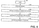
- FIG. 6 is a flowchart of a method for manufacturing an integrated circuit device, such as integrated circuit device 200 shown in FIGs. 2 through 4 .
- the process(es) illustrated in FIG. 6 may be implemented (in whole or in part) using one or more general, multi-purpose, or single-purpose processors. Unless specifically stated, the methods described herein are not constrained to a particular order or sequence. In addition, some of the described method(s) or elements thereof can occur or be performed concurrently.
- Sub-assembly 302 is an exemplary sub-assembly, which includes electrically-conductive structure 205 that is arranged to facilitate electrical communication between one or more dies 202 and one or more leads 204.
- electrically-conductive structure 205 may be soldered to one or more dies 202 and one or more leads 204.
- an electrically-conductive housing such as housing 208 (shown in FIGs. 2 -4 ).
- the electrically-conductive housing has an interior surface defining a cavity, such as interior surface 207, and an exterior surface, such as exterior surface 209.
- housing 208 is a rectangular, aluminum-composite case.
- a potting material such as potting material 206 (shown in FIGs. 2-4 ) is dispensed into the cavity defined by the interior surface.
- potting material 206 is an epoxy.
- the sub-assembly is disposed in the cavity, at block 608, in such a manner that space exists between the sub-assembly and the interior surface of the electrically-conductive housing.
- the space is occupied by the potting material.
- Sub-assembly 302 may be arranged in the cavity defined by interior surface 307 either before or after potting material 206 is disposed therein. Potting material may be self-curing or may be cured in a separate step (not shown).
- Integrated circuit devices, and manufacturing method(s) therefor have been described herein.
- Lightweight, inexpensive, electrically isolated, external device packaging provides significant thermal conduction paths.
- using a potting compound instead of another substance (such as an inert gas) gives better thermal properties.
- the device(s) may be mounted directly to other heat sinks without the need for electrical isolation, so that cooling via the external packaging itself may be used alone, or to supplement cooling provided for larger areas.
- the integrated circuit device(s) may operate at more desirable temperatures without significant alterations in packaging footprints, and/or without additional isolation requirements, reducing the need for product re-designs.
- the device(s) may be through-hole mountable.
- integrated circuit device 200 is referred to as a power rectifier, and is described as having a specific geometry, but any analog or digital integrated circuit device of any geometrical configuration may benefit from the packaging described herein.
Landscapes
- Cooling Or The Like Of Semiconductors Or Solid State Devices (AREA)
- Structures Or Materials For Encapsulating Or Coating Semiconductor Devices Or Solid State Devices (AREA)
- Casings For Electric Apparatus (AREA)
Description
- One cause of reduced efficiency in integrated circuit devices such as rectifiers is inadequate cooling during normal operation.
FIG. 1 is a perspective view of one package option for a Vishay® Semiconductor brand dual high-voltage rectifier device 10 having two semiconductor dies (not visible) inside, manufactured by Vishay Intertechnology, Inc.Device 10 is through-hole mountable via leads 14 (although surface-mountable packaging options are available), and includes anexterior epoxy housing 12 and an aluminum-composite heat sink 16. Heatsink 16 may form one side ofhousing 12, or be attached thereto. During operation ofdevice 10, heat generated by the dies is transferred throughleads 14,housing 12, andheat sink 16. The thermal conductivity ofhousing 12 is generally significantly less than that ofheat sink 16, however, which may result in areas ofdevice 10 having unsatisfactory thermal dissipation performance. - There are needs for integrated circuit devices, such as semiconductor devices, with package designs incorporating lightweight, electrically-isolated heat sinks that can be used in both surface-mountable and through-hole-mountable applications to satisfactorily dissipate heat from multiple surfaces of a device, including the housing thereof.
- It will be appreciated that the claimed subject matter is not limited to implementations that solve any or all of the disadvantages of specific integrated circuit device packaging designs or aspects thereof.
- Aspects of surface- and through-hole-mountable integrated circuits, such as bridge rectifier devices, are discussed herein. In particular, integrated circuit devices, and methods for manufacturing such integrated circuit devices according to
claims 1 and 10 are disclosed. In one implementation, an integrated circuit device (a rectifier, for example) includes a die, a lead, and an electrically-conductive structure (such as a copper die pad) arranged to facilitate electrical communication between the die and the lead. The device also includes a potting material, in which the electrically conductive structure, the die, and at least part of the lead are embedded. An electrically-conductive housing (such as an aluminum Similar semiconductor devices and power semiconductor modules are known from the referencesUS-3,569,797 ,US 5 744 860 andUS 3 271 638 . composite housing) encases the potting material and forms exterior packaging of the device. During manufacturing, the electrically-conductive structure, the die, and at least part of the lead may be arranged within the electrically-conductive housing either before or after the potting material is disposed in the housing. - When the integrated circuit device is operating, heat is removable from the die via a thermal conduction path formed by the electrically-conductive structure, the potting material, and the electrically-conductive housing.
- This Summary is provided to introduce a selection of concepts in simplified form. The concepts are further described in the Detailed Description section.
-
-
FIG. 1 is a perspective view of general packaging for a through-hole-mountable integrated circuit device. -
FIG. 2 is a plan view of an interior cross-section of an exemplary integrated circuit device having a thermally-conductive housing forming the exterior packaging thereof. -
FIG. 3 is a cross-sectional side view, in the direction of arrows 3-3, of the integrated circuit device shown inFIG. 2 . -
FIG. 4 is a perspective view of the integrated circuit device shown inFIGs. 2 and 3 . -
FIG. 5 is a diagram illustrating certain thermal conduction paths through which heat is removed from the integrated circuit device shown inFIGs. 2 - 4 (which has been rotated 90 degrees in the direction ofarrow 5, shown inFIG. 3 ) during normal operation of the integrated circuit device. -
FIG. 6 is a flowchart of a method for manufacturing the integrated circuit device shown inFIGs. 2 - 4 . - Turning to the drawings, where like numerals designate like components,
FIG. 2 is a plan view of an interior cross-section of an exemplary integrated circuit device 200 (referred to for discussion purposes as a power rectifier). Elements ofdevice 200 are briefly introduced, and the elements are discussed in further detail below. -
Device 200 includes twodies 202; three leads 204; an electrically-conductive structure 205, which is arranged to facilitate electrical communication between one ormore dies 202 and one ormore leads 204;potting material 206, in which electrically-conductive structure 205,dies 202, and portions ofleads 204 are embedded; and an electrically-conductive housing 208, which encasespotting material 206 and forms exterior packaging ofdevice 200.Housing 208 has aninterior surface 207 and anexterior surface 209.Structure 210, which may be composed of the same or different material as the interior and/or exterior surfaces of electrically-conductive housing 208, extends fromhousing 208 and provides additional heat removal capability (discussed further below, in connection withFIG. 5 ) during normal operation ofdevice 200. -
Dies 202 are similar to those found within commercially available analog or digital integrated circuit chips. As such,dies 202 are generally composed of a base material, such as a semiconductor material, and at least two electrodes (not shown), which are conductors used to make electrical contact with one or more circuits on the dies that perform predetermined functions (signal rectification, for example). -
Leads 204 facilitate electrical interconnection between electronic components external todevice 200 and the electrodes ofdies 202.Leads 204 are generally composed in whole or in part of a conductive material such as copper. As shown, portions ofleads 204 extending external todevice 200 are configured to allowdevice 200 to be mounted to a substrate (not shown) using through-hole-mounting techniques, to facilitate electrical interconnection with electronic components external todevice 200. - Inside
device 200, a portion of eachlead 204 is electrically interconnected to the electrode(s) of adie 202, either directly or indirectly, via electrically-conductive structure 205. As shown, electrically-conductive structure 205 is a rectangular, copper die pad. In general, however, electrically-conductive structure 205 may be any now-known structure, in any geometric shape, which is composed in whole or in part of a conductive material. Examples of such structures include die pads, solder balls, lead frames, or portions of leads. -
FIG. 3 is a cross-sectional side view ofdevice 200 in the direction of arrows 3-3, illustrating an exemplary arrangement of electrically-conductive structure 205 that facilitates electrical communication between die(s) 202 and the portions ofleads 204 insidedevice 200. One die 202 and twoleads 204 are visible inFIG. 3 . One side of die 202 faces electrically-conductive structure 205, and another side of die 202faces lead 204. Electrode(s) on die 202 make contact withlead 204 and electrically-conductive structure 205. Anotherlead 204 makes contact with the same side of electrically-conductive structure 205 that the side of die 202 faces. Although one electrically-conductive structure 205 is shown, it will be appreciated that more than one such structure may be present. - With continuing reference to
FIGs. 2 and 3 , in one implementation, one or more die(s) 202, lead(s) 204, and electrically-conductive structure(s) 205 may be arranged to form a sub-assembly 302 (shown inFIG. 3 ).Sub-assembly 302 is arranged withininterior surface 207 of electrically-conductive housing 208, which defines a cavity. Sub-assembly 302 is arranged in such a manner that space exists between it andinterior surface 207 of electrically-conductive housing 208.Sub-assembly 302 may be arranged in the cavity defined byinterior surface 207 either before or afterpotting material 206 is disposed therein.Potting material 206 is any suitable dielectric, thermally conductive material, such as epoxy. -
Exterior surface 209 of electrically-conductive housing 208 is composed of the same or different material and/or geometry thaninterior surface 207. As shown, both the interior and exterior surfaces are formed by an aluminum composite material, and have rectangular geometries.Optional structure 210, which extends the heat removal capacity ofdevice 200, is integral with and extends from electrically-conductive housing 208. -
FIG. 4 is a perspective view ofintegrated circuit device 200. As shown,exterior surface 209 of electrically-conductive housing 208 forms five sides (only three sides are visible) of the exterior packaging ofdevice 200, along withoptional structure 210. The sixth side includespotting material 206 and portions ofleads 204 that extend fromdevice 200. -
FIG. 5 is a diagram illustrating certain thermal conduction paths through which heat is removed fromintegrated circuit device 200, which has been rotated 90 degrees in the direction ofarrow 5, shown inFIG. 3 . Whendevice 200 is in normal operation, heat is removed to the ambient environment from die 202 via thermal conduction paths (depicted byarrows conductive structure 205,potting material 206, and interior andexterior surfaces housing 208. Heat is also transferred fromdies 202 along a thermal conduction path (depicted by arrows 504) that includesoptional structure 210, and a thermal conduction path (depicted by arrows 510) that includesleads 204. - With continued reference to
FIGs. 1-5 ,FIG. 6 is a flowchart of a method for manufacturing an integrated circuit device, such asintegrated circuit device 200 shown inFIGs. 2 through 4 . The process(es) illustrated inFIG. 6 may be implemented (in whole or in part) using one or more general, multi-purpose, or single-purpose processors. Unless specifically stated, the methods described herein are not constrained to a particular order or sequence. In addition, some of the described method(s) or elements thereof can occur or be performed concurrently. - The method begins at
oval 600, and continues atblock 602, where a sub-assembly is formed. Sub-assembly 302 (shown inFIG. 3 ) is an exemplary sub-assembly, which includes electrically-conductive structure 205 that is arranged to facilitate electrical communication between one or more dies 202 and one or more leads 204. In one implementation, electrically-conductive structure 205 may be soldered to one or more dies 202 and one or more leads 204. - Next, at block 704, an electrically-conductive housing, such as housing 208 (shown in
FIGs. 2 -4 ), is provided. The electrically-conductive housing has an interior surface defining a cavity, such asinterior surface 207, and an exterior surface, such asexterior surface 209. In one implementation,housing 208 is a rectangular, aluminum-composite case. - At
block 606, a potting material, such as potting material 206 (shown inFIGs. 2-4 ) is dispensed into the cavity defined by the interior surface. In one implementation,potting material 206 is an epoxy. - The sub-assembly is disposed in the cavity, at
block 608, in such a manner that space exists between the sub-assembly and the interior surface of the electrically-conductive housing. The space is occupied by the potting material.Sub-assembly 302 may be arranged in the cavity defined by interior surface 307 either before or after pottingmaterial 206 is disposed therein. Potting material may be self-curing or may be cured in a separate step (not shown). - Integrated circuit devices, and manufacturing method(s) therefor have been described herein. Lightweight, inexpensive, electrically isolated, external device packaging provides significant thermal conduction paths. Generally, using a potting compound instead of another substance (such as an inert gas) gives better thermal properties. The device(s) may be mounted directly to other heat sinks without the need for electrical isolation, so that cooling via the external packaging itself may be used alone, or to supplement cooling provided for larger areas. The integrated circuit device(s) may operate at more desirable temperatures without significant alterations in packaging footprints, and/or without additional isolation requirements, reducing the need for product re-designs. The device(s) may be through-hole mountable.
- Although the subject matter herein has been described in language specific to structural features and/or methodological acts, it is also to be understood that the subject matter defined in the claims is not necessarily limited to the specific features or acts described above. Rather, the specific features and acts described above are disclosed as example forms of implementing the claims. For example, integrated
circuit device 200 is referred to as a power rectifier, and is described as having a specific geometry, but any analog or digital integrated circuit device of any geometrical configuration may benefit from the packaging described herein.
Claims (13)
- An integrated circuit device (200), comprising:two or more dies (202);leads (204) having distal end adapted for mounting to a substrate using a through-hole mounting technique;an electrically-conductive structure (205) arranged to facilitate electrical communication between the dies (202) and a lead (204), wherein electrodes of the dies (202) are indirectly electrically connected to a proximate end of the lead (204) via the electrically-conductive structure (205);the two or more dies (202), the leads (204) and the electrically-conductive structure forming a sub-assembly (302).a potting material (206) having the electrically-conductive structure (205), the dies (202), and at least part of the leads (204) embedded therein, the potting material being a dielectric, thermally-conductive material; andan electrically-conductive housing (208) having an interior surface (207) and encasing the potting material (206) and arranged to form exterior packaging of the integrated circuit device (200), the sub-assembly (302) being arranged in such a manner that space exists between the sub-assembly (302) and the interior surface (207) of the electrically-conductive (208);wherein heat is removable from the dies (202) via a thermal conduction path formed by the electrically-conductive structure (205), the potting material (206), and the electrically-conductive housing (208).
- The integrated circuit device (200) according to claim l, wherein the electrically-conductive housing (208) encases a majority of a surface area of the potting material (206).
- The integrated circuit device (200) according to claim 1, wherein the dies (202) comprise semiconductor dies (202) .
- The integrated circuit device (200) according to claim 1, wherein the integrated circuit device (200) comprises a rectifier.
- The integrated circuit device (200) according to claim 1, wherein the integrated circuit device (200) comprises an active device.
- The integrated circuit device (200) according to claim 1, wherein the electrically-conductive structure (205) comprises one of a copper die pad, a solder ball, a lead, and a lead frame.
- The integrated circuit device (200) according to claim 1, wherein the dielectric thermally-conductive material comprises epoxy.
- The integrated circuit device (200) according to claim 1, wherein the electrically-conductive housing (208) comprises a metal case, the metal case preferably comprising an aluminium composite case.
- The integrated circuit device (200) according to claim 1, further comprising: a structure (210) integral with and extending from the electrically-conductive housing (208), wherein heat is removable from the integrated circuit device (200) via a thermal conduction path formed by the structure (210).
- A method for manufacturing an integrated circuit device (200), the method comprising:arranging an electrically-conductive structure (205) to facilitate electrical communication between two or more dies (202) and leads (204), the electrically-conductive structure (205), the dies (202) and the leads (204) forming a sub-assembly, wherein the leads (204) have distal ends adapted for mounting to a substrate using through-hole mounting technique;providing an electrically-conductive housing (208) having an interior surface (207) and an exterior surface (209), the interior surface (207) defining a cavity;dispensing a potting material (206) into the cavity, the potting material being a dielectric, thermally-conductive material; anddisposing the sub-assembly (302) in the cavity in such a manner that space exists between the sub-assembly (302) and the interior surface (207), the space occupied by the potting material (206).
- The method according to claim 10, further comprising: curing the potting material (206).
- The method according to claim 10, wherein the step of dispensing the potting material (206) into the cavity is performed prior to or after the step of disposing the sub-assembly (302) in the cavity.
- The method according to claim 10, wherein the step of arranging the electrically-conductive structure (205) to facilitate electrical communication between the dies (202) and the leads (204) and to form a sub-assembly (302) comprises: soldering the electrically-conductive structure (205) to the dies (202) and to the leads (204).
Applications Claiming Priority (2)
| Application Number | Priority Date | Filing Date | Title |
|---|---|---|---|
| US11/582,699 US8198709B2 (en) | 2006-10-18 | 2006-10-18 | Potted integrated circuit device with aluminum case |
| PCT/US2007/017765 WO2008048384A2 (en) | 2006-10-18 | 2007-08-10 | Potted integrated circuit device with aluminum case |
Publications (3)
| Publication Number | Publication Date |
|---|---|
| EP2078308A2 EP2078308A2 (en) | 2009-07-15 |
| EP2078308A4 EP2078308A4 (en) | 2014-03-12 |
| EP2078308B1 true EP2078308B1 (en) | 2022-12-14 |
Family
ID=39314574
Family Applications (1)
| Application Number | Title | Priority Date | Filing Date |
|---|---|---|---|
| EP07811242.2A Active EP2078308B1 (en) | 2006-10-18 | 2007-08-10 | Potted integrated circuit device with aluminum case |
Country Status (6)
| Country | Link |
|---|---|
| US (2) | US8198709B2 (en) |
| EP (1) | EP2078308B1 (en) |
| CN (1) | CN101578702B (en) |
| ES (1) | ES2938582T3 (en) |
| TW (1) | TW200828538A (en) |
| WO (1) | WO2008048384A2 (en) |
Families Citing this family (5)
| Publication number | Priority date | Publication date | Assignee | Title |
|---|---|---|---|---|
| US8421214B2 (en) * | 2007-10-10 | 2013-04-16 | Vishay General Semiconductor Llc | Semiconductor device and method for manufacturing a semiconductor device |
| DE102008045139A1 (en) * | 2008-09-01 | 2010-03-04 | Endress + Hauser Flowtec Ag | Opto-electronic device with a built-in safety device |
| US9335427B2 (en) | 2013-11-22 | 2016-05-10 | General Electric Company | High voltage shielding to enable paschen region operation for neutron detection systems |
| TWI593067B (en) * | 2014-02-26 | 2017-07-21 | 林朋科技股份有限公司 | Semiconductor package structure |
| CN106920781A (en) * | 2015-12-28 | 2017-07-04 | 意法半导体有限公司 | Semiconductor package body and the method for forming semiconductor package body |
Citations (1)
| Publication number | Priority date | Publication date | Assignee | Title |
|---|---|---|---|---|
| US5744860A (en) * | 1996-02-06 | 1998-04-28 | Asea Brown Boveri Ag | Power semiconductor module |
Family Cites Families (20)
| Publication number | Priority date | Publication date | Assignee | Title |
|---|---|---|---|---|
| US2758261A (en) * | 1952-06-02 | 1956-08-07 | Rca Corp | Protection of semiconductor devices |
| US2903630A (en) * | 1956-09-21 | 1959-09-08 | Rca Corp | Semiconductor devices |
| US2981875A (en) * | 1957-10-07 | 1961-04-25 | Motorola Inc | Semiconductor device and method of making the same |
| US3255394A (en) * | 1962-06-15 | 1966-06-07 | Gen Motors Corp | Transistor electrode connection |
| US3271638A (en) * | 1963-11-04 | 1966-09-06 | Emil M Murad | Encased semiconductor with heat conductive and protective insulative encapsulation |
| US3569797A (en) * | 1969-03-12 | 1971-03-09 | Bendix Corp | Semiconductor device with preassembled mounting |
| USRE28145E (en) * | 1972-10-25 | 1974-09-03 | Tharman rectifier network assembly | |
| US4314270A (en) * | 1977-12-02 | 1982-02-02 | Mitsubishi Denki Kabushiki Kaisha | Hybrid thick film integrated circuit heat dissipating and grounding assembly |
| US4766479A (en) * | 1986-10-14 | 1988-08-23 | Hughes Aircraft Company | Low resistance electrical interconnection for synchronous rectifiers |
| JPH0724112B2 (en) * | 1988-12-19 | 1995-03-15 | ローム株式会社 | How to install the laser diode unit |
| US5001299A (en) * | 1989-04-17 | 1991-03-19 | Explosive Fabricators, Inc. | Explosively formed electronic packages |
| EP0788127B1 (en) * | 1995-07-18 | 2004-05-06 | Omron Corporation | Electronic appliance and production method therefor |
| KR100192180B1 (en) * | 1996-03-06 | 1999-06-15 | 김영환 | Buttom lead package of multi layer |
| US6404065B1 (en) | 1998-07-31 | 2002-06-11 | I-Xys Corporation | Electrically isolated power semiconductor package |
| JP2002532893A (en) * | 1998-12-17 | 2002-10-02 | コーニンクレッカ フィリップス エレクトロニクス エヌ ヴィ | Light engine |
| JP3400427B2 (en) * | 2000-11-28 | 2003-04-28 | 株式会社東芝 | Electronic component unit and printed wiring board device mounted with electronic component unit |
| US6882041B1 (en) * | 2002-02-05 | 2005-04-19 | Altera Corporation | Thermally enhanced metal capped BGA package |
| JP2003264265A (en) * | 2002-03-08 | 2003-09-19 | Mitsubishi Electric Corp | Power semiconductor devices |
| TWI257181B (en) * | 2003-07-28 | 2006-06-21 | Rohm Co Ltd | Semiconductor module |
| JP4338620B2 (en) * | 2004-11-01 | 2009-10-07 | 三菱電機株式会社 | Semiconductor device and manufacturing method thereof |
-
2006
- 2006-10-18 US US11/582,699 patent/US8198709B2/en active Active
-
2007
- 2007-08-10 ES ES07811242T patent/ES2938582T3/en active Active
- 2007-08-10 WO PCT/US2007/017765 patent/WO2008048384A2/en not_active Ceased
- 2007-08-10 EP EP07811242.2A patent/EP2078308B1/en active Active
- 2007-08-10 CN CN200780038940.8A patent/CN101578702B/en not_active Expired - Fee Related
- 2007-08-28 TW TW096131848A patent/TW200828538A/en unknown
-
2012
- 2012-06-11 US US13/493,196 patent/US8426253B2/en active Active
Patent Citations (1)
| Publication number | Priority date | Publication date | Assignee | Title |
|---|---|---|---|---|
| US5744860A (en) * | 1996-02-06 | 1998-04-28 | Asea Brown Boveri Ag | Power semiconductor module |
Also Published As
| Publication number | Publication date |
|---|---|
| CN101578702B (en) | 2015-11-25 |
| US20080093735A1 (en) | 2008-04-24 |
| US8426253B2 (en) | 2013-04-23 |
| US8198709B2 (en) | 2012-06-12 |
| EP2078308A4 (en) | 2014-03-12 |
| TW200828538A (en) | 2008-07-01 |
| WO2008048384A3 (en) | 2008-09-04 |
| ES2938582T3 (en) | 2023-04-12 |
| CN101578702A (en) | 2009-11-11 |
| WO2008048384A2 (en) | 2008-04-24 |
| EP2078308A2 (en) | 2009-07-15 |
| US20120252167A1 (en) | 2012-10-04 |
Similar Documents
| Publication | Publication Date | Title |
|---|---|---|
| JP5442368B2 (en) | IC chip package with direct lead wire | |
| KR101394205B1 (en) | Semiconductor package | |
| US8110915B2 (en) | Open cavity leadless surface mountable package for high power RF applications | |
| JP2023033351A (en) | semiconductor equipment | |
| US20100019379A1 (en) | External heat sink for bare-die flip chip packages | |
| US8426253B2 (en) | Potted integrated circuit device with aluminum case | |
| US7867908B2 (en) | Method of fabricating substrate | |
| EP2398302B1 (en) | Semiconductor device | |
| EP1696484A1 (en) | Process for assembling a double-sided circuit component | |
| US20070013053A1 (en) | Semiconductor device and method for manufacturing a semiconductor device | |
| US8865526B2 (en) | Semiconductor device and method for manufacturing a semiconductor device | |
| JP2016219535A (en) | Electronic circuit device | |
| US20060220188A1 (en) | Package structure having mixed circuit and composite substrate | |
| US20070291457A1 (en) | IC packages with internal heat dissipation structures | |
| JP6065500B2 (en) | Semiconductor device | |
| US20260090408A1 (en) | High-power electronic package with electrically isolated heatsink | |
| US20230163042A1 (en) | Package structure and packaging method | |
| KR101198848B1 (en) | Semiconductor Device and Fabricating Method thereof | |
| JP2009105327A (en) | Semiconductor device with heat sink and manufacturing method thereof | |
| JP2010177366A (en) | Flexible substrate, mounting substrate using the same, and production process of flexible substrate | |
| JP2000068423A (en) | Semiconductor device and manufacturing method thereof | |
| JP2002043469A (en) | Semiconductor device | |
| KR101473356B1 (en) | Grounding method of heat-slug | |
| JPH09219474A (en) | Semiconductor package mounting structure |
Legal Events
| Date | Code | Title | Description |
|---|---|---|---|
| PUAI | Public reference made under article 153(3) epc to a published international application that has entered the european phase |
Free format text: ORIGINAL CODE: 0009012 |
|
| 17P | Request for examination filed |
Effective date: 20090514 |
|
| AK | Designated contracting states |
Kind code of ref document: A2 Designated state(s): AT BE BG CH CY CZ DE DK EE ES FI FR GB GR HU IE IS IT LI LT LU LV MC MT NL PL PT RO SE SI SK TR |
|
| DAX | Request for extension of the european patent (deleted) | ||
| A4 | Supplementary search report drawn up and despatched |
Effective date: 20140207 |
|
| RIC1 | Information provided on ipc code assigned before grant |
Ipc: H01L 23/00 20060101ALI20140203BHEP Ipc: H01L 23/495 20060101ALI20140203BHEP Ipc: H01L 23/24 20060101AFI20140203BHEP |
|
| STAA | Information on the status of an ep patent application or granted ep patent |
Free format text: STATUS: EXAMINATION IS IN PROGRESS |
|
| 17Q | First examination report despatched |
Effective date: 20180208 |
|
| GRAP | Despatch of communication of intention to grant a patent |
Free format text: ORIGINAL CODE: EPIDOSNIGR1 |
|
| STAA | Information on the status of an ep patent application or granted ep patent |
Free format text: STATUS: GRANT OF PATENT IS INTENDED |
|
| INTG | Intention to grant announced |
Effective date: 20220622 |
|
| GRAS | Grant fee paid |
Free format text: ORIGINAL CODE: EPIDOSNIGR3 |
|
| GRAA | (expected) grant |
Free format text: ORIGINAL CODE: 0009210 |
|
| STAA | Information on the status of an ep patent application or granted ep patent |
Free format text: STATUS: THE PATENT HAS BEEN GRANTED |
|
| AK | Designated contracting states |
Kind code of ref document: B1 Designated state(s): AT BE BG CH CY CZ DE DK EE ES FI FR GB GR HU IE IS IT LI LT LU LV MC MT NL PL PT RO SE SI SK TR |
|
| REG | Reference to a national code |
Ref country code: GB Ref legal event code: FG4D |
|
| REG | Reference to a national code |
Ref country code: CH Ref legal event code: EP |
|
| REG | Reference to a national code |
Ref country code: DE Ref legal event code: R096 Ref document number: 602007061611 Country of ref document: DE |
|
| REG | Reference to a national code |
Ref country code: IE Ref legal event code: FG4D |
|
| REG | Reference to a national code |
Ref country code: AT Ref legal event code: REF Ref document number: 1538185 Country of ref document: AT Kind code of ref document: T Effective date: 20230115 |
|
| REG | Reference to a national code |
Ref country code: LT Ref legal event code: MG9D |
|
| REG | Reference to a national code |
Ref country code: ES Ref legal event code: FG2A Ref document number: 2938582 Country of ref document: ES Kind code of ref document: T3 Effective date: 20230412 |
|
| REG | Reference to a national code |
Ref country code: NL Ref legal event code: MP Effective date: 20221214 |
|
| PG25 | Lapsed in a contracting state [announced via postgrant information from national office to epo] |
Ref country code: SE Free format text: LAPSE BECAUSE OF FAILURE TO SUBMIT A TRANSLATION OF THE DESCRIPTION OR TO PAY THE FEE WITHIN THE PRESCRIBED TIME-LIMIT Effective date: 20221214 Ref country code: LT Free format text: LAPSE BECAUSE OF FAILURE TO SUBMIT A TRANSLATION OF THE DESCRIPTION OR TO PAY THE FEE WITHIN THE PRESCRIBED TIME-LIMIT Effective date: 20221214 Ref country code: FI Free format text: LAPSE BECAUSE OF FAILURE TO SUBMIT A TRANSLATION OF THE DESCRIPTION OR TO PAY THE FEE WITHIN THE PRESCRIBED TIME-LIMIT Effective date: 20221214 |
|
| REG | Reference to a national code |
Ref country code: AT Ref legal event code: MK05 Ref document number: 1538185 Country of ref document: AT Kind code of ref document: T Effective date: 20221214 |
|
| PG25 | Lapsed in a contracting state [announced via postgrant information from national office to epo] |
Ref country code: LV Free format text: LAPSE BECAUSE OF FAILURE TO SUBMIT A TRANSLATION OF THE DESCRIPTION OR TO PAY THE FEE WITHIN THE PRESCRIBED TIME-LIMIT Effective date: 20221214 Ref country code: GR Free format text: LAPSE BECAUSE OF FAILURE TO SUBMIT A TRANSLATION OF THE DESCRIPTION OR TO PAY THE FEE WITHIN THE PRESCRIBED TIME-LIMIT Effective date: 20230315 |
|
| PG25 | Lapsed in a contracting state [announced via postgrant information from national office to epo] |
Ref country code: NL Free format text: LAPSE BECAUSE OF FAILURE TO SUBMIT A TRANSLATION OF THE DESCRIPTION OR TO PAY THE FEE WITHIN THE PRESCRIBED TIME-LIMIT Effective date: 20221214 |
|
| PG25 | Lapsed in a contracting state [announced via postgrant information from national office to epo] |
Ref country code: RO Free format text: LAPSE BECAUSE OF FAILURE TO SUBMIT A TRANSLATION OF THE DESCRIPTION OR TO PAY THE FEE WITHIN THE PRESCRIBED TIME-LIMIT Effective date: 20221214 Ref country code: PT Free format text: LAPSE BECAUSE OF FAILURE TO SUBMIT A TRANSLATION OF THE DESCRIPTION OR TO PAY THE FEE WITHIN THE PRESCRIBED TIME-LIMIT Effective date: 20230414 Ref country code: EE Free format text: LAPSE BECAUSE OF FAILURE TO SUBMIT A TRANSLATION OF THE DESCRIPTION OR TO PAY THE FEE WITHIN THE PRESCRIBED TIME-LIMIT Effective date: 20221214 Ref country code: CZ Free format text: LAPSE BECAUSE OF FAILURE TO SUBMIT A TRANSLATION OF THE DESCRIPTION OR TO PAY THE FEE WITHIN THE PRESCRIBED TIME-LIMIT Effective date: 20221214 Ref country code: AT Free format text: LAPSE BECAUSE OF FAILURE TO SUBMIT A TRANSLATION OF THE DESCRIPTION OR TO PAY THE FEE WITHIN THE PRESCRIBED TIME-LIMIT Effective date: 20221214 |
|
| PG25 | Lapsed in a contracting state [announced via postgrant information from national office to epo] |
Ref country code: SK Free format text: LAPSE BECAUSE OF FAILURE TO SUBMIT A TRANSLATION OF THE DESCRIPTION OR TO PAY THE FEE WITHIN THE PRESCRIBED TIME-LIMIT Effective date: 20221214 Ref country code: PL Free format text: LAPSE BECAUSE OF FAILURE TO SUBMIT A TRANSLATION OF THE DESCRIPTION OR TO PAY THE FEE WITHIN THE PRESCRIBED TIME-LIMIT Effective date: 20221214 Ref country code: IS Free format text: LAPSE BECAUSE OF FAILURE TO SUBMIT A TRANSLATION OF THE DESCRIPTION OR TO PAY THE FEE WITHIN THE PRESCRIBED TIME-LIMIT Effective date: 20230414 |
|
| REG | Reference to a national code |
Ref country code: DE Ref legal event code: R097 Ref document number: 602007061611 Country of ref document: DE |
|
| PLBE | No opposition filed within time limit |
Free format text: ORIGINAL CODE: 0009261 |
|
| STAA | Information on the status of an ep patent application or granted ep patent |
Free format text: STATUS: NO OPPOSITION FILED WITHIN TIME LIMIT |
|
| PG25 | Lapsed in a contracting state [announced via postgrant information from national office to epo] |
Ref country code: DK Free format text: LAPSE BECAUSE OF FAILURE TO SUBMIT A TRANSLATION OF THE DESCRIPTION OR TO PAY THE FEE WITHIN THE PRESCRIBED TIME-LIMIT Effective date: 20221214 |
|
| 26N | No opposition filed |
Effective date: 20230915 |
|
| PG25 | Lapsed in a contracting state [announced via postgrant information from national office to epo] |
Ref country code: SI Free format text: LAPSE BECAUSE OF FAILURE TO SUBMIT A TRANSLATION OF THE DESCRIPTION OR TO PAY THE FEE WITHIN THE PRESCRIBED TIME-LIMIT Effective date: 20221214 |
|
| PG25 | Lapsed in a contracting state [announced via postgrant information from national office to epo] |
Ref country code: MC Free format text: LAPSE BECAUSE OF FAILURE TO SUBMIT A TRANSLATION OF THE DESCRIPTION OR TO PAY THE FEE WITHIN THE PRESCRIBED TIME-LIMIT Effective date: 20221214 |
|
| REG | Reference to a national code |
Ref country code: CH Ref legal event code: PL |
|
| PG25 | Lapsed in a contracting state [announced via postgrant information from national office to epo] |
Ref country code: MC Free format text: LAPSE BECAUSE OF FAILURE TO SUBMIT A TRANSLATION OF THE DESCRIPTION OR TO PAY THE FEE WITHIN THE PRESCRIBED TIME-LIMIT Effective date: 20221214 |
|
| PG25 | Lapsed in a contracting state [announced via postgrant information from national office to epo] |
Ref country code: LU Free format text: LAPSE BECAUSE OF NON-PAYMENT OF DUE FEES Effective date: 20230810 |
|
| PG25 | Lapsed in a contracting state [announced via postgrant information from national office to epo] |
Ref country code: LU Free format text: LAPSE BECAUSE OF NON-PAYMENT OF DUE FEES Effective date: 20230810 Ref country code: CH Free format text: LAPSE BECAUSE OF NON-PAYMENT OF DUE FEES Effective date: 20230831 |
|
| REG | Reference to a national code |
Ref country code: BE Ref legal event code: MM Effective date: 20230831 |
|
| REG | Reference to a national code |
Ref country code: IE Ref legal event code: MM4A |
|
| PG25 | Lapsed in a contracting state [announced via postgrant information from national office to epo] |
Ref country code: IE Free format text: LAPSE BECAUSE OF NON-PAYMENT OF DUE FEES Effective date: 20230810 |
|
| PG25 | Lapsed in a contracting state [announced via postgrant information from national office to epo] |
Ref country code: IE Free format text: LAPSE BECAUSE OF NON-PAYMENT OF DUE FEES Effective date: 20230810 |
|
| PG25 | Lapsed in a contracting state [announced via postgrant information from national office to epo] |
Ref country code: BE Free format text: LAPSE BECAUSE OF NON-PAYMENT OF DUE FEES Effective date: 20230831 |
|
| PG25 | Lapsed in a contracting state [announced via postgrant information from national office to epo] |
Ref country code: BG Free format text: LAPSE BECAUSE OF FAILURE TO SUBMIT A TRANSLATION OF THE DESCRIPTION OR TO PAY THE FEE WITHIN THE PRESCRIBED TIME-LIMIT Effective date: 20221214 |
|
| PG25 | Lapsed in a contracting state [announced via postgrant information from national office to epo] |
Ref country code: BG Free format text: LAPSE BECAUSE OF FAILURE TO SUBMIT A TRANSLATION OF THE DESCRIPTION OR TO PAY THE FEE WITHIN THE PRESCRIBED TIME-LIMIT Effective date: 20221214 |
|
| PG25 | Lapsed in a contracting state [announced via postgrant information from national office to epo] |
Ref country code: HU Free format text: LAPSE BECAUSE OF FAILURE TO SUBMIT A TRANSLATION OF THE DESCRIPTION OR TO PAY THE FEE WITHIN THE PRESCRIBED TIME-LIMIT; INVALID AB INITIO Effective date: 20070810 |
|
| PG25 | Lapsed in a contracting state [announced via postgrant information from national office to epo] |
Ref country code: CY Free format text: LAPSE BECAUSE OF FAILURE TO SUBMIT A TRANSLATION OF THE DESCRIPTION OR TO PAY THE FEE WITHIN THE PRESCRIBED TIME-LIMIT; INVALID AB INITIO Effective date: 20070810 |
|
| PGFP | Annual fee paid to national office [announced via postgrant information from national office to epo] |
Ref country code: ES Payment date: 20250905 Year of fee payment: 19 |
|
| PGFP | Annual fee paid to national office [announced via postgrant information from national office to epo] |
Ref country code: DE Payment date: 20250722 Year of fee payment: 19 |
|
| PGFP | Annual fee paid to national office [announced via postgrant information from national office to epo] |
Ref country code: IT Payment date: 20250728 Year of fee payment: 19 |
|
| PGFP | Annual fee paid to national office [announced via postgrant information from national office to epo] |
Ref country code: GB Payment date: 20250724 Year of fee payment: 19 |
|
| PGFP | Annual fee paid to national office [announced via postgrant information from national office to epo] |
Ref country code: FR Payment date: 20250721 Year of fee payment: 19 |
|
| REG | Reference to a national code |
Ref country code: DE Ref legal event code: R079 Ref document number: 602007061611 Country of ref document: DE Free format text: PREVIOUS MAIN CLASS: H01L0023240000 Ipc: H10W0076470000 |
|
| PG25 | Lapsed in a contracting state [announced via postgrant information from national office to epo] |
Ref country code: TR Free format text: LAPSE BECAUSE OF FAILURE TO SUBMIT A TRANSLATION OF THE DESCRIPTION OR TO PAY THE FEE WITHIN THE PRESCRIBED TIME-LIMIT Effective date: 20221214 |