EP2075821A2 - Sample holder, method for observation and inspection, and apparatus for observation and inspection - Google Patents
Sample holder, method for observation and inspection, and apparatus for observation and inspection Download PDFInfo
- Publication number
- EP2075821A2 EP2075821A2 EP08254133A EP08254133A EP2075821A2 EP 2075821 A2 EP2075821 A2 EP 2075821A2 EP 08254133 A EP08254133 A EP 08254133A EP 08254133 A EP08254133 A EP 08254133A EP 2075821 A2 EP2075821 A2 EP 2075821A2
- Authority
- EP
- European Patent Office
- Prior art keywords
- sample
- sample holder
- film
- holder
- set forth
- Prior art date
- Legal status (The legal status is an assumption and is not a legal conclusion. Google has not performed a legal analysis and makes no representation as to the accuracy of the status listed.)
- Ceased
Links
- 238000000034 method Methods 0.000 title claims abstract description 39
- 238000007689 inspection Methods 0.000 title abstract description 29
- 238000010894 electron beam technology Methods 0.000 claims description 49
- 239000004615 ingredient Substances 0.000 claims description 27
- 229910052581 Si3N4 Inorganic materials 0.000 claims description 18
- HQVNEWCFYHHQES-UHFFFAOYSA-N silicon nitride Chemical compound N12[Si]34N5[Si]62N3[Si]51N64 HQVNEWCFYHHQES-UHFFFAOYSA-N 0.000 claims description 18
- 230000001678 irradiating effect Effects 0.000 claims description 16
- 238000010884 ion-beam technique Methods 0.000 claims description 13
- 238000001514 detection method Methods 0.000 claims description 10
- 239000007788 liquid Substances 0.000 abstract description 30
- 239000003814 drug Substances 0.000 abstract description 13
- 238000004626 scanning electron microscopy Methods 0.000 abstract 3
- 238000004627 transmission electron microscopy Methods 0.000 abstract 3
- 239000000523 sample Substances 0.000 description 366
- 239000010408 film Substances 0.000 description 141
- 239000003550 marker Substances 0.000 description 17
- 238000004519 manufacturing process Methods 0.000 description 14
- XUIMIQQOPSSXEZ-UHFFFAOYSA-N Silicon Chemical compound [Si] XUIMIQQOPSSXEZ-UHFFFAOYSA-N 0.000 description 13
- 229910052710 silicon Inorganic materials 0.000 description 13
- 239000010703 silicon Substances 0.000 description 13
- 239000000758 substrate Substances 0.000 description 12
- WGTYBPLFGIVFAS-UHFFFAOYSA-M tetramethylammonium hydroxide Chemical compound [OH-].C[N+](C)(C)C WGTYBPLFGIVFAS-UHFFFAOYSA-M 0.000 description 10
- VYPSYNLAJGMNEJ-UHFFFAOYSA-N Silicium dioxide Chemical compound O=[Si]=O VYPSYNLAJGMNEJ-UHFFFAOYSA-N 0.000 description 9
- 238000005229 chemical vapour deposition Methods 0.000 description 9
- 229920002120 photoresistant polymer Polymers 0.000 description 9
- 229910052814 silicon oxide Inorganic materials 0.000 description 9
- QAOWNCQODCNURD-UHFFFAOYSA-N Sulfuric acid Chemical compound OS(O)(=O)=O QAOWNCQODCNURD-UHFFFAOYSA-N 0.000 description 8
- 230000005540 biological transmission Effects 0.000 description 7
- 238000003384 imaging method Methods 0.000 description 7
- 238000002474 experimental method Methods 0.000 description 6
- 239000002184 metal Substances 0.000 description 6
- 229910052751 metal Inorganic materials 0.000 description 6
- 102000004169 proteins and genes Human genes 0.000 description 6
- 108090000623 proteins and genes Proteins 0.000 description 6
- 239000010409 thin film Substances 0.000 description 6
- 239000000853 adhesive Substances 0.000 description 5
- 230000001070 adhesive effect Effects 0.000 description 5
- 238000004891 communication Methods 0.000 description 5
- 230000006378 damage Effects 0.000 description 5
- 238000001878 scanning electron micrograph Methods 0.000 description 5
- PCHJSUWPFVWCPO-UHFFFAOYSA-N gold Chemical compound [Au] PCHJSUWPFVWCPO-UHFFFAOYSA-N 0.000 description 4
- 239000010931 gold Substances 0.000 description 4
- 229910052737 gold Inorganic materials 0.000 description 4
- 238000005516 engineering process Methods 0.000 description 3
- 239000007789 gas Substances 0.000 description 3
- 239000001307 helium Substances 0.000 description 3
- 229910052734 helium Inorganic materials 0.000 description 3
- SWQJXJOGLNCZEY-UHFFFAOYSA-N helium atom Chemical compound [He] SWQJXJOGLNCZEY-UHFFFAOYSA-N 0.000 description 3
- 150000002500 ions Chemical class 0.000 description 3
- 238000001020 plasma etching Methods 0.000 description 3
- 239000002210 silicon-based material Substances 0.000 description 3
- OKTJSMMVPCPJKN-UHFFFAOYSA-N Carbon Chemical compound [C] OKTJSMMVPCPJKN-UHFFFAOYSA-N 0.000 description 2
- KRHYYFGTRYWZRS-UHFFFAOYSA-N Fluorane Chemical compound F KRHYYFGTRYWZRS-UHFFFAOYSA-N 0.000 description 2
- 239000007864 aqueous solution Substances 0.000 description 2
- 229910052799 carbon Inorganic materials 0.000 description 2
- 239000002131 composite material Substances 0.000 description 2
- 239000004205 dimethyl polysiloxane Substances 0.000 description 2
- 235000013870 dimethyl polysiloxane Nutrition 0.000 description 2
- 239000004519 grease Substances 0.000 description 2
- 239000000203 mixture Substances 0.000 description 2
- 239000002245 particle Substances 0.000 description 2
- 229920000435 poly(dimethylsiloxane) Polymers 0.000 description 2
- 238000005086 pumping Methods 0.000 description 2
- 238000000851 scanning transmission electron micrograph Methods 0.000 description 2
- 238000001039 wet etching Methods 0.000 description 2
- 238000003917 TEM image Methods 0.000 description 1
- 230000002542 deteriorative effect Effects 0.000 description 1
- 238000010586 diagram Methods 0.000 description 1
- 238000007599 discharging Methods 0.000 description 1
- 229940079593 drug Drugs 0.000 description 1
- 238000001312 dry etching Methods 0.000 description 1
- 239000000428 dust Substances 0.000 description 1
- 238000005530 etching Methods 0.000 description 1
- 238000001198 high resolution scanning electron microscopy Methods 0.000 description 1
- 238000001746 injection moulding Methods 0.000 description 1
- 239000012212 insulator Substances 0.000 description 1
- 238000001393 microlithography Methods 0.000 description 1
- CXQXSVUQTKDNFP-UHFFFAOYSA-N octamethyltrisiloxane Chemical compound C[Si](C)(C)O[Si](C)(C)O[Si](C)(C)C CXQXSVUQTKDNFP-UHFFFAOYSA-N 0.000 description 1
- 238000004987 plasma desorption mass spectroscopy Methods 0.000 description 1
- 230000003014 reinforcing effect Effects 0.000 description 1
- 239000000243 solution Substances 0.000 description 1
- 125000006850 spacer group Chemical group 0.000 description 1
- XLYOFNOQVPJJNP-UHFFFAOYSA-N water Substances O XLYOFNOQVPJJNP-UHFFFAOYSA-N 0.000 description 1
Images









Classifications
-
- H—ELECTRICITY
- H01—ELECTRIC ELEMENTS
- H01J—ELECTRIC DISCHARGE TUBES OR DISCHARGE LAMPS
- H01J37/00—Discharge tubes with provision for introducing objects or material to be exposed to the discharge, e.g. for the purpose of examination or processing thereof
- H01J37/02—Details
- H01J37/20—Means for supporting or positioning the object or the material; Means for adjusting diaphragms or lenses associated with the support
-
- H—ELECTRICITY
- H01—ELECTRIC ELEMENTS
- H01J—ELECTRIC DISCHARGE TUBES OR DISCHARGE LAMPS
- H01J37/00—Discharge tubes with provision for introducing objects or material to be exposed to the discharge, e.g. for the purpose of examination or processing thereof
- H01J37/26—Electron or ion microscopes; Electron or ion diffraction tubes
-
- H—ELECTRICITY
- H01—ELECTRIC ELEMENTS
- H01J—ELECTRIC DISCHARGE TUBES OR DISCHARGE LAMPS
- H01J2237/00—Discharge tubes exposing object to beam, e.g. for analysis treatment, etching, imaging
- H01J2237/20—Positioning, supporting, modifying or maintaining the physical state of objects being observed or treated
- H01J2237/2002—Controlling environment of sample
- H01J2237/2003—Environmental cells
- H01J2237/2004—Biological samples
-
- H—ELECTRICITY
- H01—ELECTRIC ELEMENTS
- H01J—ELECTRIC DISCHARGE TUBES OR DISCHARGE LAMPS
- H01J2237/00—Discharge tubes exposing object to beam, e.g. for analysis treatment, etching, imaging
- H01J2237/20—Positioning, supporting, modifying or maintaining the physical state of objects being observed or treated
- H01J2237/2005—Seal mechanisms
-
- H—ELECTRICITY
- H01—ELECTRIC ELEMENTS
- H01J—ELECTRIC DISCHARGE TUBES OR DISCHARGE LAMPS
- H01J2237/00—Discharge tubes exposing object to beam, e.g. for analysis treatment, etching, imaging
- H01J2237/20—Positioning, supporting, modifying or maintaining the physical state of objects being observed or treated
- H01J2237/201—Positioning, supporting, modifying or maintaining the physical state of objects being observed or treated for mounting multiple objects
-
- H—ELECTRICITY
- H01—ELECTRIC ELEMENTS
- H01J—ELECTRIC DISCHARGE TUBES OR DISCHARGE LAMPS
- H01J2237/00—Discharge tubes exposing object to beam, e.g. for analysis treatment, etching, imaging
- H01J2237/20—Positioning, supporting, modifying or maintaining the physical state of objects being observed or treated
- H01J2237/204—Means for introducing and/or outputting objects
-
- H—ELECTRICITY
- H01—ELECTRIC ELEMENTS
- H01J—ELECTRIC DISCHARGE TUBES OR DISCHARGE LAMPS
- H01J2237/00—Discharge tubes exposing object to beam, e.g. for analysis treatment, etching, imaging
- H01J2237/20—Positioning, supporting, modifying or maintaining the physical state of objects being observed or treated
- H01J2237/206—Modifying objects while observing
-
- H—ELECTRICITY
- H01—ELECTRIC ELEMENTS
- H01J—ELECTRIC DISCHARGE TUBES OR DISCHARGE LAMPS
- H01J2237/00—Discharge tubes exposing object to beam, e.g. for analysis treatment, etching, imaging
- H01J2237/26—Electron or ion microscopes
- H01J2237/262—Non-scanning techniques
-
- H—ELECTRICITY
- H01—ELECTRIC ELEMENTS
- H01J—ELECTRIC DISCHARGE TUBES OR DISCHARGE LAMPS
- H01J2237/00—Discharge tubes exposing object to beam, e.g. for analysis treatment, etching, imaging
- H01J2237/26—Electron or ion microscopes
- H01J2237/28—Scanning microscopes
Definitions
- the present invention relates to a sample holder permitting a sample to be observed and inspected using an electron beam or ion beam at high resolution in a case where the sample contains moisture or other liquid component.
- the invention also relates to a method of observation and inspection using this sample holder.
- the invention relates to an observation and inspection apparatus using the sample holder.
- a sample to be observed or inspected is placed in a sample chamber whose pressure is reduced by vacuum pumping. Under this condition, the sample is irradiated with an electron beam. As a result, secondary signals such as backscattered electrons and secondary electrons are emitted from the sample. These secondary signals are detected.
- SEM scanning electron microscope
- TEM transmission electron microscope
- STEM scanning transmission electron microscope
- the sample In observing or inspecting a sample using such an apparatus, the sample is exposed to a reduced-pressure ambient within a sample chamber. Accordingly, when a sample containing moisture is to be observed or inspected, if the sample is intact placed within the specimen chamber that is a reduced-pressure ambient, water evaporates off from the sample. This hinders observation or inspection of the sample under the condition where it contains moisture.
- patent references 1 and 2 One example of method of observing or inspecting a sample using SEM without exposing a sample to a reduced-pressure ambient in this way is shown in patent references 1 and 2.
- the inside of a sample chamber is divided into an atmospheric-pressure ambient and a vacuum ambient using a film that transmits an electron beam but does not transmit gas.
- the sample is placed in the atmospheric-pressure ambient.
- the sample placed in the atmospheric-pressure ambient is irradiated with an electron beam from the vacuum ambient, the beam impinging on the sample via the film.
- Backscattered electrons are produced from the irradiated sample.
- the backscattered electrons pass through the film and are detected by a backscattered electron detector mounted in the vacuum ambient. Consequently, an SEM image is obtained.
- the conventional TEM sample holder has used carbon films and mesh.
- the sample is placed in an environment that has been pumped down to some extent, then good results will be obtained.
- it has been difficult to obtain 1 atm pressure resistance.
- the sample holder is assembled fully manually, requiring much labor. Hence, it is impossible to cope with a large number of samples. Because the sample holder is assembled manually, it is difficult to reduce the spacing between the carbon films. As a result, there arises the problem that the resolution is deteriorated.
- the problem common to SEM and TEM is that a sample of more than 1 milliliter is required when the sample is passed through a filter or a medicine is mixed into the sample.
- a sample holder for use in SEM uses a thin film less than 10 nm thick and so secondary electrons can be detected. Consequently, imaging and inspection can be performed at higher resolution.
- a sample holder for use in TEM permits the distance between thin films to be reduced. Hence, high-resolution imaging and inspection are enabled.
- the common feature to SEM and TEM sample holders is that a sample containing liquid and placed under atmospheric pressure can be observed or inspected after a small amount of the sample is passed through a filter or a medicine is mixed with the sample.
- a large number of sample holders can be fabricated because of use of MEMS or nanoimprint technology. It would be desirable to provide such a sample holder. It would also be desirable to provide a method of observing or inspecting a sample using such a sample holder. It would be further desirable to provide an apparatus for observing or inspecting a sample using such a sample holder.
- a first sample holder according to the present invention has a framelike member provided with an opening that is covered with a film.
- the film has a first surface on which a sample is held.
- the thickness D of the film and the length L of the outer periphery of the portion of the film that covers the opening in the framelike member satisfy a relationship given by L/D ⁇ 200, 000.
- a second sample holder has a framelike member provided with an opening in which a lattice is formed. At least opening portions of the lattice are covered with a film.
- the film has a first surface on which a sample is held.
- the thickness D of the film and the length L of the outer periphery of the portion of the film that covers the opening portions in the lattice satisfy a relationship given by L/D ⁇ 200,000.
- a third sample holder according to the invention has two sample holder components disposed opposite to each other such that a sample can be held between the holder components.
- Each of the sample holder components has the same structure as the first or second sample holder described above.
- a fourth sample holder according to the invention has a sample holder component having the same structure as the aforementioned first or second sample holder and a base disposed opposite to the sample holder component.
- a sample-holding space is formed between the sample holder component and the base.
- a channel for supplying a sample into the sample-holding space is formed. The sample can be supplied from the outside into the sample-holding space via the channel.
- a fifth sample holder according to the invention has two sample holder components disposed opposite to each other and a sample-holding space formed between the two holder components.
- Each of the holder components has the same structure as the aforementioned first or second sample holder.
- a channel for supplying a sample into the sample-holding space is formed. The sample can be supplied from the outside into the sample-holding space via the channel.
- a sixth sample holder according to the invention is characterized in that at least one of the aforementioned channel and sample-holding space has a filter structure that discriminates ingredients in the sample.
- a first method of observing or inspecting a sample in accordance with the present invention comprises preparing one of the above-described first, second, and fourth sample holders, holding a sample on the first surface of the film, and irradiating the sample with a primary beam via a second surface of the film, thus observing or inspecting the sample.
- a second method of observing or inspecting a sample in accordance with the present invention comprises preparing one of the above-described third and fifth sample holders, reducing the pressure outside the sample holder, holding the sample on the sample holder, and irradiating the sample with a primary beam under this condition, thus observing or inspecting the sample.
- a first observation-and-inspection apparatus has support means for supporting one of the first, second, and fourth sample holders, primary beam irradiation means for irradiating a sample with a primary beam via the film of the sample holder, and signal detection means for detecting a secondary signal produced from the sample in response to the primary beam irradiation.
- a second observation-and-inspection apparatus has support means for supporting one of the above-described first, second, and fourth sample holders, a vacuum chamber for reducing the pressure of an ambient in contact with the second surface of the film of the sample holder, primary beam irradiation means connected with the vacuum chamber and irradiating the sample held on the first surface of the film with the primary beam via the film, and signal detection means for detecting a secondary signal produced from the sample in response to the primary beam irradiation.
- a third observation-and-inspection apparatus has support means for supporting one of the above-described third and fifth sample holders, primary beam irradiation means for irradiating the sample with a primary beam via the film of the sample holder, and signal detection means for detecting a secondary signal produced from the sample in response to the primary beam irradiation or a signal transmitted through the sample, thus obtaining information about the sample.
- a fourth observation-and-inspection apparatus has support means for supporting one of the above-described third and fifth sample holders, a vacuum chamber for reducing the pressure of an ambient in contact with a side of the film of the sample holder not opposite to the sample, primary beam irradiation means connected with the vacuum chamber and irradiating the sample with a primary beam via the film, and signal detection means for detecting a secondary signal produced from the sample in response to the primary beam irradiation or a signal transmitted through the sample, thus obtaining information about the sample.
- the opening in the framelike member or the opening portions in the lattice are coated with the film.
- the relationship between the thickness D of the film and the length D of the outer periphery of the portion of the film that covers the opening in the film or the opening portions in the lattice is given by L/D ⁇ 200,000. Therefore, if the film is thinned, the film can sufficiently withstand a pressure difference of greater than 1 atm. As a result, in observation or inspection using a primary beam such as in SEM or TEM, high resolution can be obtained.
- Microlithography can be done by forming the film by an MEMS process including silicon nitride or by a nanoimprint process. Therefore, where the sample is passed through a filter or a medicine is mixed into the sample, the amount of sample can be reduced. Furthermore, sample holders can be mass-produced by making use of MEMS process or nanoimprint process.
- Fig. 1 shows a sample holder 102 according to the present embodiment and an experimental tool for performing pressure resistance experiments on the sample holder.
- a sample-holding film 101 is formed on the sample holder 102.
- a sample (not shown) is placed on a first surface of the film 101. Fundamentally, the sample is placed under atmospheric pressure (atmospheric-pressure ambient).
- a primary beam (electron beam or ion beam) is directed at the sample via the sample-holding film 101 and so the ambient in contact with a second surface of the sample-holding film 101 needs to be pumped down to a vacuum to permit passage of the primary beam while preventing scattering. Therefore, the sample-holding film 101 needs to withstand a differential pressure (i.e., the difference between the pressures of the ambients in contact with the surfaces) of at least 1 atm. In the present invention, it has been determined with some allowance that a resistance withstanding a pressure difference of 2 atm. is highly desirable. Conditions under which this resistance is obtained have been found.
- the experiments were performed as shown in Fig. 1 .
- the sample holder 102 having a framelike member 102a forming the body of the holder 102 and the sample-holding film 101 providing a cover over an opening 102b formed in the framelike member 102a was sandwiched between O-rings 103 and 104, which were held down by cases 105 and 106, respectively. Consequently, gas was prevented from flowing between spaces 107 and 108.
- the surface of the sample-holding film 102 in contact with the space 108 is herein referred to as the first surface. A sample was held or placed on this first surface. Accordingly, the pressure in the space 108 was increased while maintaining the atmospheric pressure in the space 107. The pressure at which the sample-holding film 101 was destroyed was measured.
- the experiment was repeated with various parameters which are various values of the thickness D ( ⁇ m) and various values of the length L ( ⁇ m) of the outer periphery of the film at the boundary with the sample-holding film or with a lattice.
- the length L is defined as follows.
- Fig. 2 is a view of the sample-holding body 102 as viewed from the direction of the space 107.
- the length of the outer periphery 110 is L. That is, the length of the outer periphery 110 of the sample-holding film 101 that covers the opening 102b in the framelike member 102a is L.
- L is the length of the outer periphery 112. That is, the length of the outer periphery of the portion of the sample-holding film 101 that covers opening portions 111b in the lattice 111 is L.
- the experimental results have shown that in the case of L/D ⁇ 200,000, a pressure resistance withstanding 2 atm or higher can be accomplished. It is considered that a realistic maximum value of the length L is about 20 mm where the production yield is taken into account.
- the corresponding minimum value of the thickness D is 100 nm. If the thickness D is greater than this value, scattering due to the sample-holding film 101 is increased conspicuously, deteriorating resolution in observation or inspection. Consequently, it is desired that the thickness D be set smaller than 100 nm.
- the thickness D is as small as 10 nm but the length L is less than 2,000 ⁇ m or where the thickness D is as small as 1 nm but the length L is 200 ⁇ m
- the sample-holding film 101 is not destroyed. Under this condition, if an electron beam is directed at the sample through the second surface, secondary electrons emitted from the sample pass through the sample-holding film 101.
- the mean free path of secondary electrons is of the order of 10 nm.
- the secondary electrons can be detected by a secondary electron detector placed in an ambient (vacuum chamber) in contact with the second surface, and a secondary electron image can be obtained.
- the thickness D is preferably set less than 10 nm.
- the thickness D is preferably set greater than 1 nm.
- only thick films could be formed, and secondary electron images could not be produced.
- Backscattered electron images have been used, and the resolution has been low.
- secondary electrons can be employed and, therefore, observation and inspection can be done at high resolution.
- sample holders can be mass-produced because they are fabricated using MEMS processes.
- a method of fabricating a sample holder is described by referring to Fig. 5 .
- a silicon substrate 201 is mirror-polished on its both surfaces. Films of silicon nitride 211 and 212 are formed on both surfaces of the substrate using chemical vapor deposition (CVD) ( Fig. 5(a) ). After lithographically forming a resist pattern 221 using a photoresist, the silicon nitride film 211 is selectively etched using the resist pattern as a mask by RIE (reactive ion etching) ( Fig. 5(b) ).
- RIE reactive ion etching
- the silicon substrate 201 is wet-etched using the silicon nitride film 211 as a mask and using KOHsolution ( Fig. 5(c) ).
- a sample holder having the silicon nitride film 212 can be fabricated by the present sequence of processing steps.
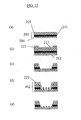
- a method of fabricating a sample holder including a thin film on which a lattice is formed is next described. Both surfaces of an SOI (silicon-on-insulator) wafer 202 ( Fig. 6(a) ) are mirror-polished. Silicon nitride films 211 and 212 are formed on both surfaces of the wafer 202 using chemical vapor deposition (CVD) ( Fig. 6(a) ).
- SOI silicon-on-insulator
- a resist pattern 221 is formed lithographically using a photoresist. Thereafter, the silicon nitride film 211 is selectively etched using the resist pattern as a mask by RIE ( Fig. 6(b) ). After removing the resist pattern 221 with sulfuric acid, a silicon substrate 203 is wet-etched using the silicon nitride film 211 as a mask and using KOH solution.
- the silicon oxide film 231 is selectively removed using BHF (buffered hydrofluoric acid) ( Fig. 6(c) ). After a resist is sprayed on the surface, a pattern of a lattice is lithographically formed. Using the resist pattern 222 as a mask, silicon 204 is selectively etched using aqueous solution of TMAH (tetramethyl ammonium hydroxide) ( Fig. 6(d) ). Finally, the resist pattern 222 is removed with sulfuric acid. Consequently, the pattern of the lattice can be formed. This permits the length L of the outer periphery of the holding film to be reduced. Therefore, the holding film can be thinned.
- BHF bufferetramethyl ammonium hydroxide
- a silicon substrate 201 whose both surfaces have beenmirror-polished is prepared.
- Silicon nitride films 211 and 212 are formed on the both surfaces of the silicon substrate 201 by chemical vapor deposition (CVD).
- CVD chemical vapor deposition
- a silicon oxide film 232 is formed on one surface using CVD ( Fig. 7(a) ).
- a resist pattern 223 of a lattice is lithographically formed on the silicon oxide film 232 using a photoresist ( Fig. 7(b) ).
- the silicon oxide film 232 is selectively removed by wet etching using BHF to form a lattice pattern.
- the resist is removed using sulfuric acid ( Fig. 7(c) ).
- a photoresist is applied to the other side.
- a resist pattern 221 is formed lithographically using the photoresist.
- the silicon substrate 201 is etched by a method similar to the method of forming a sample holder having no lattice ( Fig. 7(e) ).
- aqueous solution of TMAH that does not etch silicon oxide was used instead of KOH.
- the present process permits the lattice to be formed without using an expensive SOI wafer.
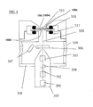
- the apparatus includes an electron optics column 305, a backscattered electron detector 306, a secondary electron detector 307, a vacuum chamber 308, a sample driving mechanism 309, and the sample holder 150 described in Embodiment 2.
- the electron optics column 305 includes an electron source 301, a condenser lens 302, an objective lens 303, and a scanning unit 304.
- the sample holder 150 is in contact with the vacuum chamber 308 via O-rings 310 and 311 that form support means for supporting the sample holder 150. Therefore, the inside of the chamber 308 can be pumped down to a vacuum or to a reduced-pressure level.
- the sample holder 150 is composed of a framelike member 150a forming the body of the holder and a sample-holding film 150c in the same way as the foregoing sample holder.
- the framelike member 150a is provided with an opening 150b covered with the sample-holding film 150c.
- a sample 315 containing liquid, for example, is held on the sample-holding film 150c. Because of this structure, when an electron beam 320 is directed at the sample 315 in an atmospheric-pressure ambient via the sample-holding film 150c of the sample holder 150, backscattered electrons and secondary electrons produced from the sample 315 can be detected. Consequently, a high-resolution SEM image of the sample 315 in the atmospheric-pressure ambient can be obtained.
- an electron beam isused. Imaging can also be done using an ion beam. Especially, using a focused helium ion beam, observation can be made with less damage to the sample-holding film 150c.
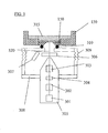
- the configuration of the present embodiment is schematically shown in Fig. 9 .
- the present embodiment is similar to Embodiment 3 except for the following point.
- the sample holder is held from above and below it using the O-rings 310 and 311.
- the O-ring 310 forming support means is disposed between the sample holder 150 and the vacuum chamber 3 08.
- a laboratory dish 130 is disposed around the sample 315 containing liquid to prevent the sample 315 from spilling out. Because of these features, when the inside of the chamber 308 is pumped down, the reduced-pressure state can be maintained only with the O-ring 310. In consequence, the sample holder can be held easily.
- grease can be used. In the following embodiments, grease can be similarly used.
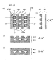
- Fig. 10(a) is a top plan view of the holder.
- Fig. 10 (b) is a cross-sectional view taken on line A-A' of Fig. 10(a).
- Fig. 10(c) is a cross-sectional view taken on line B-B' of Fig. 10(a).
- Fig. 10 (d) is a cross-sectional view taken on line C-C' of Fig. 10(a) .
- the sample holder 151 is composed of a holder base 401 and a holder cap 402.
- the base 401 has an entrance 408a, an exit 408b, and a channel 408c.
- the cap 402 is provided with an opening 413a. Consequently, a part of the film 411 is exposed.
- a sample-holding space 408d is located under the opening 413a in the film 411.
- the sample holder 151 is fabricated by a method similar to the method of Embodiment 2.
- the holder base 401 and the holder cap 402 are formed independently by a method similar to the method of Embodiment 2. However, when the holder base 401 is formed, etching of silicon is stopped during the process. The depth of the channel 408c is controlled.
- the holder base 401 and holder cap 402 fabricated in this way are adhesively bonded as shown in Fig. 10 .
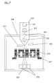
- pipes 422a and 422b are connected with the entrance 408a and exit 408b, respectively, of the sample holder 151.
- a sample is supplied into the channel 408c in the sample holder 151 via the pipe 422a connected with the entrance 408a.
- the sample is appropriately expelled from the pipe 422b connected with the exit 408b of the channel 408c.
- Fig. 12 The whole structure of the observation-and-inspection apparatus using this sample holder is shown in Fig. 12 .
- This structure is fundamentally similar to the structure of Embodiment 4 except that no laboratory dish is used and that a channel is used to prevent the sample containing liquid from spilling out.
- a sample can be easily inserted into the sample holder 151.
- the sample 414 disposed in the channel 408c within the sample holder 151 can be irradiated and scanned with a focused electron beam 320 via the opening 413a.
- Backscattered electrons or secondary electrons induced by the electron beam 320 can be detected by a backscattered electron detector 306 or a secondary electron detector 307. Consequently, an SEM image of the sample 414 can be obtained.
- This structure permits the sample containing liquid to be observed or inspected.
- the configuration of the present embodiment is similar to Embodiment 5 except that a lattice structure is disposed on the thin filmportion of the sample holder 151. Because of this structure, a thin film of reduced thickness can be used.
- Amethodof fabricating the present sample holder is as follows.
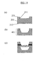
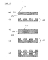
- the holder cap 402 is formed by steps similar to the steps of Embodiment 2 (see Fig. 13 ). Also, the holder base 401 is formed (see Fig. 14 ). Finally, the holder base 401 and holder cap 402 are bonded together adhesively (see Fig. 14 ).
- Fig. 15 (b) is a cross-sectional view taken on line A-A' of Fig. 15 (a).
- Fig. 15 (c) isacross-sectional viewtakenonlineB-B' of Fig. 15 (a).
- Fig. 15 (d) isacross-sectional view taken on line C-C' of Fig. 15(a) .
- the sample holder is fabricated in the same way as in Embodiment 6.
- the method is schematically illustrated in Fig. 16 .
- Fig. 17 schematically shows the manner in which pipes 422a and 422b for introducing samples into the cell are connected. Because of this structure, plural samples can be efficiently observed or inspected.
- the present embodiment is similar to Embodiment 5 except that an electron beam can be emitted downward from above (see Fig. 18 ) . Because of this structure, intrusion of dust into the electron optics column can be suppressed.
- FIG. 19(a) is a top plan view of the holder 153.
- Fig. 19(b) is a cross-sectional view taken on line A-A' of Fig. 19(a).
- Fig. 19(c) is a cross-sectional view taken on line B-B' of Fig. 19(a) .
- the present sample holder 153 is fabricated by a method similar to the method of Embodiment 5.
- a delivery port 408e is formed in addition to the entrance 408a and exit 408b.
- branching channels 430, 431 and a delivery channel 408f are formed in addition to the channel 408c.
- the depth of the branching channels i.e., the width extending perpendicularly to the film 411) is set smaller than the depth of the channel 408c.
- the thickness of observation portions 455 located immediately under the film 411 i.e., the width extending perpendicularly to the film 411, is set to 10 nm to 20 ⁇ m. More preferably, the thickness of the observation portions is set larger than the size of the ingredients included in the sample by a factor of 1.1 to 1.2. Consequently, when a sample containing a liquid component is introduced into the sample holder 153, the ingredients to be observed or inspected are brought close to the film 411. This can reduce the degree to which the electron beam is scattered by the liquid component interposed between the film 411 and the ingredients. As a result, a good SEM image can be obtained from over the whole inside of each observation portion. Where the sample contains atmosphere, the principle of the present embodiment can be similarly applied.
- the depth of the observation portions 455 located immediately under the film 411 i.e., the width of the branching channels 430 and 431 extending perpendicularly to the film 411, is set to 10 nm to 5 ⁇ m. This reduces the path of the electron beam within the sample holder 153 when a sample containing a liquid component is introduced into the sample holder 153. Consequently, the degree to which the electron beam is scattered by liquid and gas can be reduced. Hence, a good SEM image can be obtained from over the whole inside of each observation region.
- Fig. 20 is a cross-sectional view of the sample holder 154 of the present embodiment.
- the structure of the present sample holder is similar to the structure of Embodiment 9 except that the depth (width extending perpendicularly to the film 411) of some parts of the branching channels 430 and 431 varies continuously and that the holder base 403 is made of PDMS (polydimethyl siloxane) to provide such continuous control of the depth.
- PDMS polydimethyl siloxane
- ingredients within the sample containing liquid can be smoothly guided to the observation portions.
- Ingredients having different sizes can be placed at different positions by continuously varying the depth, especially immediately under the observation portions. Consequently, observation and inspection can be facilitated.
- a sample holder 155 according to the present embodiment is similar to the sample holder of Embodiment 9 except that filters 462a, 462b, 462c, and 462d are mounted respectively in the branching channels 430 of small cross section connected with the channel 408c as shown in Fig. 21 .
- Protrusive pillars 415 shown in Fig. 21 are mounted as these filters. The spacing between the protrusive pillars is different among the filters 462a, 462b, 462c, and 462d.
- the protrusive members are not limited to pillars. Convex members can also be mounted. Furthermore, balls may be mounted.
- a sample holder 156 of the present embodiment is similar to the sample holder of Embodiment 11 except that filters 463a, 463b, 463c, and 463d different from the filters 462a-462d are disposed in the portions located between the observation portions 455 of the branching channels 430 and the delivery passage 408f (see Fig. 22 ).
- These filters are made of protrusive members in the same way as in Embodiment 11. In one feature of Embodiment 12, however, the spacing between the protrusive members of the filters 463a-463d is smaller than the spacing between the protrusive members of the aforementioned filters 462a-462d.
- the sample holder of the present embodiment operates as follows. First, a sample is introduced from the entrance 408a toward the exit 408b to fill the channel 408c with the sample, in the same way as in Embodiment 11. Then, the delivery port 408e is pumped down. The branching channels 430 in communication with the observation portions 455 are filled with the sample. At this time, the filters 462a-462d permit ingredients having different sizes to pass into the locations under the observation portions 455.
- the pressures at the entrance 408a, exit 408b, and delivery port 408e are made substantially equal. Under this condition, the sample is discharged from the exit 408b. At this time, the sample is left at the observation portions 455 but the sample is eliminated from the channel 408c. In this state, the delivery port 408e is pumped down. Consequently, only the liquid component can be discharged from the delivery port 408e through the branching channels 430 and through the delivery channel 408f via the filters 463a-463d. As a result, only ingredients having no liquid component can be left at the observation portions 455.
- the electron beam 320 incident on the film 411 is scattered by the liquid.
- liquid is selectively discharged and only ingredients can be brought to the observation portions 455. Therefore, scattering due to liquid can be prevented. Consequently, the electron beam 320 is less scattered. In consequence, observation and inspection can be performed at improved resolution.
- a sample holder 151 is placed inside a vacuum chamber 308 (see Fig. 23 ).
- a stage 313 forming support means is mounted to move the sample holder 151.
- the entrance 308a and exit 308b are sealed off.
- the sample 315 can be easily tilted and observed or inspected (see Fig. 24 ).
- the present embodiment is similar to Embodiment 7 except that an index pattern 180 is formed on a part of the sample holder 157 to indicate dimensional references by means of dimensional indicia.
- the configuration of the sample holder 157 according to the present embodiment is shown in Fig. 25 .
- a reference pattern (index pattern) 180 providing references for lengths is formed on the surface of the sample holder 157 near each observation portion 455.
- An example of the reference pattern for lengths is shown in Fig. 26 and includes sets of lines having different intervals.
- the present embodiment is similar to Embodiment 4 except that the sample 315 is pretreated and marked with a fluorescent marker and that a fluorescent detector 325 is added to the detector ( Fig. 27 ).
- a fluorescent detector 325 is added to the detector ( Fig. 27 ).
- antibodies to which a fluorescent marker is attached is added to the sample by making use of an antigen-antibody reaction.
- the fluorescent marker When the sample is irradiated with a focused electron beam, the fluorescent marker produces cathodoluminescent emission. The emitted light is detected by the fluorescent detector 325.
- the fluorescent detector 325 In the present embodiment, when an observation or inspection is performed, backscattered or secondary electrons are first detected. The focus or stigmation of the electron beam 320 is adjusted. Then, the fluorescent spot is identified using the fluorescent detector 325.
- the present embodiment is similar to Embodiment 15 except that a metal marker is attached during the pretreatment.
- a metal marker is attached during the pretreatment.
- an antibody to which gold marker has been attached is added to the sample by making use of an antigen-antibody reaction.
- gold particles having diameters of 10 to 50 nm are used as the marker.
- the metal marker When a focused electron beam is directed at the sample, the metal marker is larger in atomic weight than biological portions. Consequently, the marker can be clearly observed as a backscattered electron image. This makes it possible to know where the protein of interest or its composite are located. Furthermore, the protein or its composites and its surroundings can be observed or inspected in detail.
- Fig. 28(a) is a top plan view of the sample holder 160.
- Fig. 28(b) is a cross-sectional view taken on line A-A' of Fig. 28(a) .
- the holder is provided with an entrance 408a for a sample, an exit 408b, a channel 408c, branching channels 430, 431, and observation portions 455.
- the sample is held in the observation portions 455.
- a pipe 422 for supplying the sample and another pipe 422 for discharging the sample can be connected with the entrance 408a and exit 408b, respectively, in the same way as in Embodiment 7.
- a channel 408c is formed between the entrance 408a and exit 408b. The sample is injected from the entrance 408a and expelled from the exit 408b through the channel 408c.
- Each observation portion 455 is made of the gap between two films disposed opposite to each other, the films transmitting an electron beam ( Fig. 28(b) ).
- a sample introduced into each observation portion 455 is irradiated with the electron beam via one film.
- the electron beam transmitted through the sample passes through the other film and goes out of the cell.
- the sample located inside each observation portion can be observed or inspected by STEM or TEM.
- FIG. 29 Channels, branchingchannels, andanobservationportion are formed in each of resinous members 491 and 492 by injection molding or nanoimprint technology ( Fig. 29(a) ).
- Adhesive, 493 and 494 is sprayed on the bonded surfaces of the resinous members 491 and 492.
- Films 495 and 496 are bonded to the resinous members 491 and 492, respectively, adhesively ( Fig. 29(b) ).
- Adhesive 497 is applied to one film 496 to permit the two films 495 and 496 to be bonded together with a slight gap therebetween. The films 495 and 496 are then bonded together.
- the adhesive is applied to only the required portions using a metal mask 498 ( Fig. 29(c) ).
- the gap between the films can be adjusted by adjusting the amount of the adhesive, its viscosity, and the pressure applied when bonding is done ( Fig. 29(d) ).
- a spacer may be interposed between the two films 495 and 496 to adjust the gap.
- extra portions of the films are cut out.
- film portions located around the centers of the channels are removed using another metal mask 499 and an ion beam 500 ( Fig. 29(e) ).
- a portion 501 becoming a channel cap is injection-molded or formed by nanoimprint technology.
- adhesive 502 is sprayed on the surface.
- the cap portion is bonded to the resinous member 491 ( Fig. 29(f) ).
- a sample holder 160 is fabricated by these steps.
- the whole structure of an apparatus for observing or inspecting an STEM image is shown in Fig. 30 .
- the apparatus includes an electron optics column 305, a vacuum chamber 308, an upper electron beam detector 503, an on-axis electron beam detector 504, off-axis electron beam detectors 506, a sample holder 160, and a stage 507 for supporting the sample holder 160.
- the stage 507 forms support means.
- the optics column 305 includes an electron source 301, a condenser lens 302, an objective lens 303, and a scanning unit 304.
- the sample inside each observation portion 455 of the sample holder 160 can be irradiated and scanned with a focused electron beam 320.
- Backscattered or secondary electrons induced by the electron beam 320 can be detected by the upper electron beam detector 503. Consequently, an SEM image of the sample can be obtained.
- an STEM image can be derived by the use of the on-axis electron beam detector 504 and off-axis electron beam detectors 506.
- Support means in which a lattice structure similar to the lattice structure of Embodiment 2 is disposed are formed to support the films 495 and 496.
- a thinner film can be used because the outer peripheries of the films can be reduced.
- the resolution can be improved further.
- an electron beam is used.
- An ion beam can also be used for observation. Especially, using a helium ion beam, observation can be made with less damage to the sample-holding film.
- an on-axis ion detector and off-axis ion detectors are used instead of the on-axis electron beam detector 504 and off-axis electron beam detectors 506, respectively.
- a sample holder 161 according to the present embodiment is similar to the sample holder of Embodiment 17 except that a delivery port 408e and a delivery passage 408f are formed in addition to the entrance 408a and exit 408b in communication with the channel 408c, in the same way as in Embodiment 9.
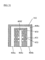
- Fig. 31(a) is a top plan view of the sample holder 161.
- Branching channels 430 and 431 of small cross section are connected with a channel 408c extending from the entrance 408a to the exit 408b.
- the branching channels 430 and 431 are connected with a delivery passage 408f that is connected with the delivery port 408e through observation portions 455.
- a sample is entered into the channel 408c by introducing the sample toward the exit 408b from the entrance 408a.
- the sample enters the branching channels 430 and 431, too, by capillarity.
- a sufficient amount of sample may not be introduced into the observation portions 455.
- a sufficient amount of sample can be entered into the observation portions 455 via the branching channels 430 and 431 by setting the pressure at the delivery port 408e lower than the pressure at the entrance 408a and exit 408b.
- a sample can be introduced into the observation portions 455 via the branching channels 430 and 431 of small cross section and so small ingredients can be observed and inspected.
- a sample holder 162 according to the present embodiment is similar to the sample holder of Embodiment 18 except that the holder 162 is made of a silicon-based material.
- the holder is shown particularly in Fig. 32.
- Fig. 32(a) is a top plan view of the holder.
- Fig. 32(b) is a cross-sectional view taken on line A-A' of Fig. 32(a) .
- a method of fabricating the present sample holder is described by referring to Fig. 33 .
- Both surfaces of a silicon substrate 201 are mirror-polished.
- Silicon nitride films 211 and 212 are formed on both surfaces of the silicon substrate 201 by CVD.
- a silicon oxide film 231 is formed on one of the silicon nitride films by CVD ( Fig. 33(a) ).
- the silicon nitride film 212 on which the silicon oxide film 231 is not formed is etched into a pattern on the side where only the silicon nitride film is formed by dry etching using a mask that has been lithographically formed using a photoresist.
- the silicon substrate 201 is etched partly by wet etching using TMAH ( Fig. 33(b) ). Then, the silicon oxide film 231 is partially processed using a mask fabricated similarly using a photoresist lithographically. Then, the silicon nitride film 211 is etched using another mask of photoresist. As a result, a geometry as shown in Fig. 3(c) is formed. The silicon substrate 201 is etched from the surface of the silicon substrate 201 on which any other film is not deposited and from the surface on which the silicon nitride film 231 is formed, using TMAH. As a result, a holder part as shown in Fig.
- a similar holder part is also fabricated.
- the two holder parts are bonded together adhesively such that their surfaces on which the silicon oxide film 231 is formed are in contact with each other.
- a sample holder 162 is completed ( Fig. 33(e) ).
- the interval between the two opposite sample-holding films is adjusted to be from 1 nm to 1 ⁇ m. If the interval is greater than 1 ⁇ m, the electron beam is scattered to a greater extent by the sample-holding film. This greatly deteriorates the resolution. Where the interval is smaller than 1 nm, the sample cannot be inserted between the films. Because the sample holder is made of a silicon-based material in this way, the fabrication process can be simplified.
- the present embodiment is similar to Embodiment 19 except that filters 462a, 462b, 462c, and 462d are mounted in the branching channels 430 of small cross section connected with the channel 408c as shown in Fig. 34 .
- Each of the filters is made of a protrusive member 415 shown in Fig. 34 .
- the spacing between the protrusive members is different among the filters 462a, 462b, 462c, and 462d.
- sample ingredients having different sizes can be introduced to the observation portions 455.
- ingredients different in size canbe selectively observed or inspected.
- a sample holder 163 according to the present embodiment is similar to the sample holder of Embodiment 20 except that filters 463a, 463b, 463c, and 463d different from the filters 462a-462d are mounted between each observation portion 455 and delivery passage 408f (see Fig. 35 ).
- Each of the filters 463a-463d is made of a protrusive member 415 in the same way as in Embodiment 20.
- the spacing between the protrusive members of the filters 463a-463d is smaller than the spacing between the protrusive members of the filters 462a-462d.
- the sample holder of the present embodiment operates as follows. First, a sample is introduced from the entrance 408a toward the exit 408b to fill the channel 408c with the sample, in the same way as in Embodiment 12. Then, the delivery port 408e is pumped down. The branching channels 430 in communication with the observation portions 455 are filled with the sample. At this time, the filters 462a-462d permit ingredients having different sizes to be brought into the observation portions 455.
- the pressures at the entrance 408a, exit 408b, and delivery port 408e are made substantially equal. Under this condition, the sample is discharged from the exit 408b. At this time, the sample is left in the observation portions 455 but the sample is eliminated from the channel 408c. In this state, the delivery port 408e is pumped down. Consequently, only the liquid component can be discharged from the delivery port 408e through the delivery channel 408f via the filters 463a-463d. As a result, only ingredients having no liquid component can be left in the observation portions 455.
- the electron beam 320 incident on the film 411 is scattered by the liquid.
- liquid is selectively discharged and only ingredients can be brought into the observation portions 455. Therefore, scattering due to liquid can be prevented. Consequently, the electron beam 320 is less scattered. Thus, observation and inspection can be performed at improved resolution.
- the present embodiment is similar to Embodiment 17 except that an imaging lens 330 for focusing the electrons transmitted through the sample is added (see Fig. 36 ).
- Fig. 36 indicated by 331 is a high-sensitivity electron camera.
- an electron beam is used. Imaging can also be done using an ion beam. Especially, using a focused helium ion beam, observation can be made with less damage to the sample-holding film. In this case, a high-sensitivity ion camera is used instead of the high-sensitivity electron camera 331.
- the present embodiment is similar to Embodiment 17 except that the sample is marked with a fluorescent marker at the beginning of pretreatment and that a fluorescent detector 325 is added to the detector (see Fig. 37 ).
- a fluorescent detector 325 is added to the detector (see Fig. 37 ).
- an antibody to which a fluorescent marker has been attached is added to the sample by making use of an antigen-antibody reaction.
- the fluorescent marker When the sample is irradiated with a focused electron beam, the fluorescent marker produces cathodoluminescent emission. The emitted light is detected by the fluorescent detector 325.
- transmitted electrons are first detected.
- the focus or stigmation of the electron beam 320 is adjusted.
- the fluorescent spot is identified using the fluorescent detector 325.
- a transmission electron image is obtained using a transmitted electron detector again.
- the present embodiment is similar to Embodiment 23 except that a metal marker is attached to the sample at the beginning of pretreatment.
- a metal marker is attached to the sample at the beginning of pretreatment.
- an antibody to which gold marker has been attached is added to the sample by making use of an antigen-antibody reaction.
- gold particles having diameters of 10 to 50 nm are used as the marker.
- the metal marker When a focused electron beam is directed at the sample, the metal marker is larger in atomic weight than biological portions. Consequently, the marker can be clearly observed on a transmission electron image. Use of the marker makes it possible to identify locations where a protein of interest or its complexes are present. Furthermore, the protein or its complexes and its surroundings can be observed or inspected in detail by observing or inspecting transmitted electrons.
- a sample holder according to the present embodiment has plural entrances 408a in communication with the same channel 408c to permit a sample and a medicine to be mixed within a cell.
- the sample and medicine can be mixed (see Fig. 38 ).
- the sample and medicine can be mixed in a cell.
- the resulting mixture is introduced into a sample-holding space 455 through the channels 430.
- the surroundings of the sample-holding space 455 have a structure as described in Embodiment 5 or 17.
- the cell is installed in a sample chamber within a scanning electron microscope, a transmission electron microscope, or a scanning transmission electron microscope.
- the mixture present in the sample-holding space within the cell is irradiated with an electron beam. Produced secondary signal or transmitted electrons are detected. Thus, information about the sample can be derived.
- a sample and one medicine are mixed.
- a configuration in which a sample and plural medicines can be mixed is also possible.
- the timing at which liquid medicine is mixed with a sample can be controlled by installing flow retarders in the channels.
- the present embodiment is similar to Embodiment 25 except that the vicinities of the position where a liquid medicine and a sample are mixed can be directly observed or inspected to permit observation or inspection of the process in which the liquid medicine and sample are mixed (see Fig. 39 ).
- the whole holder is made of a silicon-based material. Because of this structure, the process in which the liquid medicine and sample react can be measured at high resolution.
- the openings 102b and 150b in the framelike members 102a and 150a are covered with the films 101 and 150c, respectively.
- the sample 315 is held on the first surface of each film.
- the thickness D of the film and the length L of the outer periphery of the portion of each film that covers the opening in the framelike member satisfy a relationship given by L/D ⁇ 200,000.
- the lattice 111 is formed in each of the openings 102b and 150b in the framelike members 102a and 150a, respectively. At least the opening portions 111b of the lattices are covered with the films 101 and 150c, respectively.
- the sample 315 is held on the first surface of each film. The thickness D of the film and the length L of the outer periphery of the portion of each film that covers the opening portions in the lattice satisfy a relationship given by L/D ⁇ 200,000.
- the thickness of each film can be set between 1 nm and 100 nm. Furthermore, the thickness of each film can be set between 1 nm and 10 nm.
- the films can be made of silicon nitride.
- the first surface of each film can be made open to permit a manipulator (not shown) having a probe to make an access to the surfaces from the outside.
- Two sample holder components each having the same structure as the above-described sample holder are prepared and placed opposite to each other. A sample can be held between the two sample holder components.
- sample holders may be prepared as a sample holder component.
- the sample holder component and a base may be disposed opposite to each other.
- a sample-holding space may be formed between the sample holder component and the base.
- a channel for supplying a sample into the sample-holding space may be formed. The sample can be supplied from the outside into the sample-holding space via the channel.
- a filter structure for discriminating ingredients in the sample can be mounted in at least one of the channel and sample-holding space.
- sample holder components each of which is the above-described sample holder may be placed opposite to each other, and a sample-holding space may be formed between the sample holder components.
- a channel for supplying a sample into the sample-holding space may be formed.
- the sample may be supplied from the outside into the sample-holding space via the channel.
- a filter structure for discriminating ingredients in the sample can be mounted in at least one of the channel and sample-holding space.
- the filter structure can have a function of discriminating the ingredients in the sample according to size. Furthermore, the filter structure can have at least one of a step portion, a tilted portion, a portion having an identified width, a pillar portion, and a portion having a function of adsorbing certain ingredients in the sample.
- a delivery passage for pulling out at least a part of the sample can be connected with the sample-holding space.
- the space between the opposite films or the interval between the film and the base can be set within a range of 0.01 ⁇ m to 1 ⁇ m.
- a method for observing or inspecting a sample according to the present invention comprises holding a sample on a first surface of the film of any one of the above-described sample holders and irradiating the sample with a primary beam via the second surface of the film.
- the primary beam can be emitted while reducing the pressure of the ambient in contact with the second surface of the film.
- the first surface of the film can be made open. This permits a manipulator (not shown) having a probe to make an access to the sample from outside of the sample holder.
- the sample held on the sample holder can be irradiated with the primary beam while reducing the pressure of the outside of the sample holder. Thus, the sample can be observed or inspected.
- An observation-and-inspection apparatus has support means for supporting any one of the above-described sample holders, primary beam irradiation means for irradiating a sample with a primary beam via the film of the sample holder, and signal detection means for detecting a secondary signal produced from the sample in response to the primary beam irradiation.
- Another observation-and-inspection apparatus has support means for supporting any one of the above-described sample holders, a vacuum chamber for reducing the pressure of an ambient in contact with the second surface of the film of the sample holder, primary beam irradiation means connected with the vacuum chamber and irradiating a sample held on the first surface of the film with a primary beam via the film, and signal detection means for detecting a secondary signal produced from the sample in response to the primary beam irradiation.
- the primary beam can be an electron beam or an ion beam.
- the secondary signal can be at least one kind of secondary electrons, backscattered electrons, and fluorescent light.
- the observation-and-inspection apparatus has primary beam irradiation means for irradiating a sample with a primary beam via the film of the sample holder supported on the support means.
- a secondary signal produced from the sample in response to the primary beam irradiation or a signal transmitted through the sample is detected. As a result, information about the sample can be obtained.
- the apparatus can have a vacuum chamber and primary beam irradiation means connected with the vacuum chamber.
- the vacuum chamber reduces the pressure of an ambient in contact with the side of the film of sample holder that is not opposite to the sample supported on the support means.
- the primary beam irradiation means irradiates the sample with a primary beam via the film.
- a secondary signal produced from the sample in response to the irradiation or a signal transmitted through the sample is detected. As a result, information about the sample can be obtained.
- the primary beam can be an electron beam or an ion beam.
- the secondary signal can be at least one kind of secondary electrons, backscattered electrons, and fluorescent light.
Landscapes
- Chemical & Material Sciences (AREA)
- Analytical Chemistry (AREA)
- Analysing Materials By The Use Of Radiation (AREA)
- Sampling And Sample Adjustment (AREA)
Abstract
Description
- The present invention relates to a sample holder permitting a sample to be observed and inspected using an electron beam or ion beam at high resolution in a case where the sample contains moisture or other liquid component. The invention also relates to a method of observation and inspection using this sample holder. Furthermore, the invention relates to an observation and inspection apparatus using the sample holder.
- In a sample inspection apparatus having the configuration of a scanning electron microscope (SEM), a sample to be observed or inspected is placed in a sample chamber whose pressure is reduced by vacuum pumping. Under this condition, the sample is irradiated with an electron beam. As a result, secondary signals such as backscattered electrons and secondary electrons are emitted from the sample. These secondary signals are detected.
- Similarly, in a sample observation apparatus or sample inspection apparatus having the configuration of a transmission electron microscope (TEM) or a scanning transmission electron microscope (STEM), a sample to be observed or inspected is placed in a sample chamber whose pressure is reduced by vacuum pumping. In TEM or STEM, the sample placed in a sample chamber is irradiated with an electron beam. The electron beam transmitted through the sample is detected.
- In observing or inspecting a sample using such an apparatus, the sample is exposed to a reduced-pressure ambient within a sample chamber. Accordingly, when a sample containing moisture is to be observed or inspected, if the sample is intact placed within the specimen chamber that is a reduced-pressure ambient, water evaporates off from the sample. This hinders observation or inspection of the sample under the condition where it contains moisture.
- One example of method of observing or inspecting a sample using SEM without exposing a sample to a reduced-pressure ambient in this way is shown in
patent references - In this method, when an observation or inspection is performed, the sample placed in the atmospheric-pressure ambient is irradiated with an electron beam from the vacuum ambient, the beam impinging on the sample via the film. Backscattered electrons are produced from the irradiated sample. The backscattered electrons pass through the film and are detected by a backscattered electron detector mounted in the vacuum ambient. Consequently, an SEM image is obtained.
- Another method is described in
patent references
[Patent reference 1]JP-A-2007-292702
[Patent reference 2]JP-A-2007-294365
[Patent reference 3]JP-A-47-24961
[Patent reference 4]JP-A-6-318445 - Where a conventional SEM sample holder as described in
patent references - On the other hand, the conventional TEM sample holder has used carbon films and mesh. In this case, if the sample is placed in an environment that has been pumped down to some extent, then good results will be obtained. However, it has been difficult to obtain 1 atm pressure resistance. Furthermore, the sample holder is assembled fully manually, requiring much labor. Hence, it is impossible to cope with a large number of samples. Because the sample holder is assembled manually, it is difficult to reduce the spacing between the carbon films. As a result, there arises the problem that the resolution is deteriorated.
- The problem common to SEM and TEM is that a sample of more than 1 milliliter is required when the sample is passed through a filter or a medicine is mixed into the sample.
- In view of the foregoing, the present invention has been made. A sample holder for use in SEM uses a thin film less than 10 nm thick and so secondary electrons can be detected. Consequently, imaging and inspection can be performed at higher resolution. A sample holder for use in TEM permits the distance between thin films to be reduced. Hence, high-resolution imaging and inspection are enabled. The common feature to SEM and TEM sample holders is that a sample containing liquid and placed under atmospheric pressure can be observed or inspected after a small amount of the sample is passed through a filter or a medicine is mixed with the sample. In addition, a large number of sample holders can be fabricated because of use of MEMS or nanoimprint technology. It would be desirable to provide such a sample holder. It would also be desirable to provide a method of observing or inspecting a sample using such a sample holder. It would be further desirable to provide an apparatus for observing or inspecting a sample using such a sample holder.
- A first sample holder according to the present invention has a framelike member provided with an opening that is covered with a film. The film has a first surface on which a sample is held. The thickness D of the film and the length L of the outer periphery of the portion of the film that covers the opening in the framelike member satisfy a relationship given by L/D < 200, 000.
- A second sample holder according to the invention has a framelike member provided with an opening in which a lattice is formed. At least opening portions of the lattice are covered with a film. The film has a first surface on which a sample is held. The thickness D of the film and the length L of the outer periphery of the portion of the film that covers the opening portions in the lattice satisfy a relationship given by L/D < 200,000.
- A third sample holder according to the invention has two sample holder components disposed opposite to each other such that a sample can be held between the holder components. Each of the sample holder components has the same structure as the first or second sample holder described above.
- A fourth sample holder according to the invention has a sample holder component having the same structure as the aforementioned first or second sample holder and a base disposed opposite to the sample holder component. A sample-holding space is formed between the sample holder component and the base. A channel for supplying a sample into the sample-holding space is formed. The sample can be supplied from the outside into the sample-holding space via the channel.
- A fifth sample holder according to the invention has two sample holder components disposed opposite to each other and a sample-holding space formed between the two holder components.
- Each of the holder components has the same structure as the aforementioned first or second sample holder. A channel for supplying a sample into the sample-holding space is formed. The sample can be supplied from the outside into the sample-holding space via the channel.
- A sixth sample holder according to the invention is characterized in that at least one of the aforementioned channel and sample-holding space has a filter structure that discriminates ingredients in the sample.
- A first method of observing or inspecting a sample in accordance with the present invention comprises preparing one of the above-described first, second, and fourth sample holders, holding a sample on the first surface of the film, and irradiating the sample with a primary beam via a second surface of the film, thus observing or inspecting the sample.
- A second method of observing or inspecting a sample in accordance with the present invention comprises preparing one of the above-described third and fifth sample holders, reducing the pressure outside the sample holder, holding the sample on the sample holder, and irradiating the sample with a primary beam under this condition, thus observing or inspecting the sample.
- A first observation-and-inspection apparatus according to the invention has support means for supporting one of the first, second, and fourth sample holders, primary beam irradiation means for irradiating a sample with a primary beam via the film of the sample holder, and signal detection means for detecting a secondary signal produced from the sample in response to the primary beam irradiation.
- A second observation-and-inspection apparatus according to the invention has support means for supporting one of the above-described first, second, and fourth sample holders, a vacuum chamber for reducing the pressure of an ambient in contact with the second surface of the film of the sample holder, primary beam irradiation means connected with the vacuum chamber and irradiating the sample held on the first surface of the film with the primary beam via the film, and signal detection means for detecting a secondary signal produced from the sample in response to the primary beam irradiation.
- A third observation-and-inspection apparatus according to the invention has support means for supporting one of the above-described third and fifth sample holders, primary beam irradiation means for irradiating the sample with a primary beam via the film of the sample holder, and signal detection means for detecting a secondary signal produced from the sample in response to the primary beam irradiation or a signal transmitted through the sample, thus obtaining information about the sample.
- A fourth observation-and-inspection apparatus according to the invention has support means for supporting one of the above-described third and fifth sample holders, a vacuum chamber for reducing the pressure of an ambient in contact with a side of the film of the sample holder not opposite to the sample, primary beam irradiation means connected with the vacuum chamber and irradiating the sample with a primary beam via the film, and signal detection means for detecting a secondary signal produced from the sample in response to the primary beam irradiation or a signal transmitted through the sample, thus obtaining information about the sample.
- In the present invention, the opening in the framelike member or the opening portions in the lattice are coated with the film. The relationship between the thickness D of the film and the length D of the outer periphery of the portion of the film that covers the opening in the film or the opening portions in the lattice is given by L/D < 200,000. Therefore, if the film is thinned, the film can sufficiently withstand a pressure difference of greater than 1 atm. As a result, in observation or inspection using a primary beam such as in SEM or TEM, high resolution can be obtained.
- Microlithography can be done by forming the film by an MEMS process including silicon nitride or by a nanoimprint process. Therefore, where the sample is passed through a filter or a medicine is mixed into the sample, the amount of sample can be reduced. Furthermore, sample holders can be mass-produced by making use of MEMS process or nanoimprint process.
- Other preferred embodiments of the invention will appear in the course of the description thereof, which follows.
-
-
Fig. 1 is a cross-sectional view of a sample holder according toEmbodiment 1 of the present invention, as well as an experimental tool for performing experiments to know the pressure resistance of the holder; -
Fig. 2 is a plan view of the sample holder according toEmbodiment 1, showing the structure of the sample holder; -
Fig. 3 is a plan view of a sample holder having a lattice according toEmbodiment 1, showing the structure of the sample holder; -
Fig. 4 is a graph showing the pressure resistance of the sample holder according toEmbodiment 1; -
Figs. 5 and6 show vertical cross sections of a sample holder according toEmbodiment 2, illustrating a method of fabricating the holder; -
Fig. 7 shows vertical cross sections of the sample holder according toEmbodiment 2, illustrating another method of fabricating the holder; -
Fig. 8 is a schematic vertical cross section of a sample holder according toEmbodiment 3, showing the whole structure of the holder; -
Fig. 9 is a schematic vertical cross section of a sample holder according toEmbodiment 4, showing the whole structure of the holder; -
Fig. 10 shows vertical cross sections of a sample holder according to Embodiment 5, showing the structure of the holder; -
Fig. 11 shows a method of connecting pipes to the sample holder according to Embodiment 5; -
Fig. 12 is a schematic vertical cross section of the sample holder according to Embodiment 5, showing the whole structure of the holder; -
Fig. 13 shows vertical cross sections of a sample holder according to Embodiment 6, illustrating a method of fabricating the holder; -
Fig. 14 shows vertical cross sections of a sample holder according to Embodiment 6, illustrating another method of fabricating the holder; -
Fig. 15 shows vertical cross sections of a sample holder according to Embodiment 7, showing the structure of the holder; -
Fig. 16 shows vertical cross sections of a sample holder according to Embodiment 7, illustrating a method of fabricating the holder; -
Fig. 17 shows a method of connecting pipes to the sample holder according to Embodiment 7; -
Fig. 18 is a vertical cross section of a sample holder according to Embodiment 8, showing the whole structure of the holder; -
Fig. 19 shows a sample holder according to Embodiment 9, showing the whole structure of the holder; -
Fig. 20 is a vertical cross section of a sample holder according to Embodiment 10, showing the structure of the holder; -
Fig. 21 shows the configuration of a sample holder according to Embodiment 11; -
Fig. 22 shows the configuration of a sample holder according to Embodiment 12; -
Fig. 23 is a vertical cross section of a sample holder according toEmbodiment 13, showing the whole structure of the holder; -
Fig. 24 is a vertical cross section similar toFig. 23 , but in which the stage has been tilted; -
Fig. 25 is a schematic view of a sample holder according to Embodiment 14, showing the whole structure of the holder; -
Fig. 26 is a diagram showing a reference pattern of lengths according to Embodiment 14; -
Fig. 27 is a cross-sectional view of a sample holder according to Embodiment 15, showing the whole structure of the holder; -
Fig. 28 shows the configuration of a sample holder according to Embodiment 17; -
Fig. 29 shows vertical cross sections of the sample holder according to Embodiment 17, illustrating a method of fabricating the holder; -
Fig. 30 is a vertical cross section of the sample holder according to Embodiment 17, showing the whole structure of the holder; -
Fig. 31 is a schematic view of a sample holder according to Embodiment 18, showing the structure of the holder; -
Fig. 32 shows the configuration of a sample holder according to Embodiment 19; -
Fig. 33 shows vertical cross sections of a sample holder according to Embodiment 19, illustrating a method of fabricating the holder; -
Fig. 34 shows the configuration of a sample holder according to Embodiment 20; -
Fig. 35 shows the configuration of a sample holder according to Embodiment 21; -
Fig. 36 is a vertical cross section of a sample holder according to Embodiment 22, showing the whole structure of the holder; -
Fig. 37 is a vertical cross section of a sample holder according to Embodiment 23, showing the whole structure of the holder; -
Fig. 38 is a schematic view of a sample holder according to Embodiment 25, showing the structure of the holder; and -
Fig. 39 is a schematic view of a sample holder according to Embodiment 26, showing the structure of the holder. - Embodiments of the present invention are hereinafter described with reference to the accompanying drawings.
-
Fig. 1 shows asample holder 102 according to the present embodiment and an experimental tool for performing pressure resistance experiments on the sample holder. A sample-holdingfilm 101 is formed on thesample holder 102. A sample (not shown) is placed on a first surface of thefilm 101. Fundamentally, the sample is placed under atmospheric pressure (atmospheric-pressure ambient). - On the other hand, a primary beam (electron beam or ion beam) is directed at the sample via the sample-holding
film 101 and so the ambient in contact with a second surface of the sample-holdingfilm 101 needs to be pumped down to a vacuum to permit passage of the primary beam while preventing scattering. Therefore, the sample-holdingfilm 101 needs to withstand a differential pressure (i.e., the difference between the pressures of the ambients in contact with the surfaces) of at least 1 atm. In the present invention, it has been determined with some allowance that a resistance withstanding a pressure difference of 2 atm. is highly desirable. Conditions under which this resistance is obtained have been found. - The experiments were performed as shown in
Fig. 1 . Thesample holder 102 having aframelike member 102a forming the body of theholder 102 and the sample-holdingfilm 101 providing a cover over anopening 102b formed in theframelike member 102a was sandwiched between O-rings cases spaces film 102 in contact with thespace 108 is herein referred to as the first surface. A sample was held or placed on this first surface. Accordingly, the pressure in thespace 108 was increased while maintaining the atmospheric pressure in thespace 107. The pressure at which the sample-holdingfilm 101 was destroyed was measured. The experiment was repeated with various parameters which are various values of the thickness D (µm) and various values of the length L (µm) of the outer periphery of the film at the boundary with the sample-holding film or with a lattice. - The length L is defined as follows.
Fig. 2 is a view of the sample-holdingbody 102 as viewed from the direction of thespace 107. In this figure, the length of theouter periphery 110 is L. That is, the length of theouter periphery 110 of the sample-holdingfilm 101 that covers theopening 102b in theframelike member 102a is L. - Referring to
Fig. 3 , where there is alattice 111 for reinforcing the sample-holdingfilm 101 in theopening 102b formed in theframelike member 102a, L is the length of theouter periphery 112. That is, the length of the outer periphery of the portion of the sample-holdingfilm 101 that covers openingportions 111b in thelattice 111 is L. - The results of the experiments are shown in
Fig. 4 . It has been found that there is a linear relationship between the destruction strength of the film and the ratio L/D and that 2 atm pressure resistance is achieved under the condition L/D < 200, 000 . Conversely, where thespace 108 was kept at the atmospheric pressure and a pressure was applied to thespace 107, the sample-holdingfilm 101 was destroyed at a lower pressure than in the case ofFig. 4 . Therefore, where the sample is placed on the surface of the sample-holdingfilm 101 in contact with thespace 108, danger of destruction of the film can be reduced. - The experimental results have shown that in the case of L/D < 200,000, a pressure resistance withstanding 2 atm or higher can be accomplished. It is considered that a realistic maximum value of the length L is about 20 mm where the production yield is taken into account. The corresponding minimum value of the thickness D is 100 nm. If the thickness D is greater than this value, scattering due to the sample-holding
film 101 is increased conspicuously, deteriorating resolution in observation or inspection. Consequently, it is desired that the thickness D be set smaller than 100 nm. - It has also been found from the results of the experiments that where the thickness D is as small as 10 nm but the length L is less than 2,000 µm or where the thickness D is as small as 1 nm but the length L is 200 µm, if a sample is placed on the first surface of the sample-holding
film 101 under atmospheric pressure and the second surface is exposed to a vacuum, the sample-holdingfilm 101 is not destroyed. Under this condition, if an electron beam is directed at the sample through the second surface, secondary electrons emitted from the sample pass through the sample-holdingfilm 101. The mean free path of secondary electrons is of the order of 10 nm. The secondary electrons can be detected by a secondary electron detector placed in an ambient (vacuum chamber) in contact with the second surface, and a secondary electron image can be obtained. - It is known that secondary electron images are sensitive to surfaces and produce high-resolution images. This can also be confirmed in the present invention. Therefore, it is more desired that the thickness D be set less than 10 nm. However, where D is reduced extremely, the production yield will be deteriorated. Accordingly, the thickness D is preferably set greater than 1 nm. In the past, only thick films could be formed, and secondary electron images could not be produced. Backscattered electron images have been used, and the resolution has been low. In the present invention, secondary electrons can be employed and, therefore, observation and inspection can be done at high resolution. In addition, sample holders can be mass-produced because they are fabricated using MEMS processes.
- A method of fabricating a sample holder is described by referring to
Fig. 5 . Asilicon substrate 201 is mirror-polished on its both surfaces. Films ofsilicon nitride Fig. 5(a) ). After lithographically forming a resistpattern 221 using a photoresist, thesilicon nitride film 211 is selectively etched using the resist pattern as a mask by RIE (reactive ion etching) (Fig. 5(b) ). After removing the resistpattern 221 with sulfuric acid, thesilicon substrate 201 is wet-etched using thesilicon nitride film 211 as a mask and using KOHsolution (Fig. 5(c) ). A sample holder having thesilicon nitride film 212 can be fabricated by the present sequence of processing steps. - A method of fabricating a sample holder including a thin film on which a lattice is formed is next described. Both surfaces of an SOI (silicon-on-insulator) wafer 202 (
Fig. 6(a) ) are mirror-polished.Silicon nitride films wafer 202 using chemical vapor deposition (CVD) (Fig. 6(a) ). - Then, a resist
pattern 221 is formed lithographically using a photoresist. Thereafter, thesilicon nitride film 211 is selectively etched using the resist pattern as a mask by RIE (Fig. 6(b) ). After removing the resistpattern 221 with sulfuric acid, asilicon substrate 203 is wet-etched using thesilicon nitride film 211 as a mask and using KOH solution. - The
silicon oxide film 231 is selectively removed using BHF (buffered hydrofluoric acid) (Fig. 6(c) ). After a resist is sprayed on the surface, a pattern of a lattice is lithographically formed. Using the resistpattern 222 as a mask,silicon 204 is selectively etched using aqueous solution of TMAH (tetramethyl ammonium hydroxide) (Fig. 6(d) ). Finally, the resistpattern 222 is removed with sulfuric acid. Consequently, the pattern of the lattice can be formed. This permits the length L of the outer periphery of the holding film to be reduced. Therefore, the holding film can be thinned. - Another method of forming the lattice is now described. A
silicon substrate 201 whose both surfaces have beenmirror-polished is prepared.Silicon nitride films silicon substrate 201 by chemical vapor deposition (CVD). Then, asilicon oxide film 232 is formed on one surface using CVD (Fig. 7(a) ). A resistpattern 223 of a lattice is lithographically formed on thesilicon oxide film 232 using a photoresist (Fig. 7(b) ). - Using the resist
pattern 223 as a mask, thesilicon oxide film 232 is selectively removed by wet etching using BHF to form a lattice pattern. The resist is removed using sulfuric acid (Fig. 7(c) ). A photoresist is applied to the other side. A resistpattern 221 is formed lithographically using the photoresist. - Using the photoresist pattern, the
silicon substrate 201 is etched by a method similar to the method of forming a sample holder having no lattice (Fig. 7(e) ). In the present process, however, aqueous solution of TMAH that does not etch silicon oxide was used instead of KOH. The present process permits the lattice to be formed without using an expensive SOI wafer. - An observation-and-inspection apparatus according to one embodiment of the present invention is schematically shown in
Fig. 8 . The apparatus includes anelectron optics column 305, abackscattered electron detector 306, asecondary electron detector 307, avacuum chamber 308, asample driving mechanism 309, and thesample holder 150 described inEmbodiment 2. Theelectron optics column 305 includes anelectron source 301, acondenser lens 302, anobjective lens 303, and ascanning unit 304. Thesample holder 150 is in contact with thevacuum chamber 308 via O-rings sample holder 150. Therefore, the inside of thechamber 308 can be pumped down to a vacuum or to a reduced-pressure level. - The
sample holder 150 is composed of a framelikemember 150a forming the body of the holder and a sample-holdingfilm 150c in the same way as the foregoing sample holder. Theframelike member 150a is provided with anopening 150b covered with the sample-holdingfilm 150c. Asample 315 containing liquid, for example, is held on the sample-holdingfilm 150c. Because of this structure, when anelectron beam 320 is directed at thesample 315 in an atmospheric-pressure ambient via the sample-holdingfilm 150c of thesample holder 150, backscattered electrons and secondary electrons produced from thesample 315 can be detected. Consequently, a high-resolution SEM image of thesample 315 in the atmospheric-pressure ambient can be obtained. - In the configuration of the present embodiment, an electron beamisused. Imaging can also be done using an ion beam. Especially, using a focused helium ion beam, observation can be made with less damage to the sample-holding
film 150c. - The configuration of the present embodiment is schematically shown in
Fig. 9 . The present embodiment is similar toEmbodiment 3 except for the following point. InEmbodiment 3, the sample holder is held from above and below it using the O-rings Embodiment 4, only the O-ring 310 forming support means is disposed between thesample holder 150 and thevacuum chamber 3 08. Furthermore, inEmbodiment 4, alaboratory dish 130 is disposed around thesample 315 containing liquid to prevent thesample 315 from spilling out. Because of these features, when the inside of thechamber 308 is pumped down, the reduced-pressure state can be maintained only with the O-ring 310. In consequence, the sample holder can be held easily. Instead of the O-ring 310, grease can be used. In the following embodiments, grease can be similarly used. - The structure of a
sample holder 151 according to the present embodiment is shown inFig. 10. Fig. 10(a) is a top plan view of the holder.Fig. 10 (b) is a cross-sectional view taken on line A-A' ofFig. 10(a). Fig. 10(c) is a cross-sectional view taken on line B-B' ofFig. 10(a). Fig. 10 (d) is a cross-sectional view taken on line C-C' ofFig. 10(a) . Thesample holder 151 is composed of aholder base 401 and aholder cap 402. Thebase 401 has anentrance 408a, anexit 408b, and achannel 408c. Thecap 402 is provided with anopening 413a. Consequently, a part of thefilm 411 is exposed. A sample-holdingspace 408d is located under theopening 413a in thefilm 411. - The
sample holder 151 is fabricated by a method similar to the method ofEmbodiment 2. Theholder base 401 and theholder cap 402 are formed independently by a method similar to the method ofEmbodiment 2. However, when theholder base 401 is formed, etching of silicon is stopped during the process. The depth of thechannel 408c is controlled. Theholder base 401 andholder cap 402 fabricated in this way are adhesively bonded as shown inFig. 10 . - As shown in
Fig. 11 ,pipes entrance 408a andexit 408b, respectively, of thesample holder 151. A sample is supplied into thechannel 408c in thesample holder 151 via thepipe 422a connected with theentrance 408a. The sample is appropriately expelled from thepipe 422b connected with theexit 408b of thechannel 408c. - The whole structure of the observation-and-inspection apparatus using this sample holder is shown in
Fig. 12 . This structure is fundamentally similar to the structure ofEmbodiment 4 except that no laboratory dish is used and that a channel is used to prevent the sample containing liquid from spilling out. - By using this structure, a sample can be easily inserted into the
sample holder 151. Thesample 414 disposed in thechannel 408c within thesample holder 151 can be irradiated and scanned with afocused electron beam 320 via theopening 413a. Backscattered electrons or secondary electrons induced by theelectron beam 320 can be detected by a backscatteredelectron detector 306 or asecondary electron detector 307. Consequently, an SEM image of thesample 414 can be obtained. This structure permits the sample containing liquid to be observed or inspected. - The configuration of the present embodiment is similar to Embodiment 5 except that a lattice structure is disposed on the thin filmportion of the
sample holder 151. Because of this structure, a thin film of reduced thickness can be used. - Amethodof fabricating the present sample holder is as follows. The
holder cap 402 is formed by steps similar to the steps of Embodiment 2 (seeFig. 13 ). Also, theholder base 401 is formed (seeFig. 14 ). Finally, theholder base 401 andholder cap 402 are bonded together adhesively (seeFig. 14 ). - Because of the configuration described so far, a holder having a thinner thin film can be fabricated. Consequently, a sample containing liquid can be observed or inspected at high resolution.
- The present embodiment is similar to Embodiment 5 except that
plural entrances 408a,plural exits 408b,plural channels 408c, and plural sample-holdingspaces 408d are all formed in the same sample holder 152 (seeFig. 15). Fig. 15 (b) is a cross-sectional view taken on line A-A' ofFig. 15 (a). Fig. 15 (c) isacross-sectional viewtakenonlineB-B' ofFig. 15 (a). Fig. 15 (d) isacross-sectional view taken on line C-C' ofFig. 15(a) . The sample holder is fabricated in the same way as in Embodiment 6. The method is schematically illustrated inFig. 16 .Fig. 17 schematically shows the manner in whichpipes - The present embodiment is similar to Embodiment 5 except that an electron beam can be emitted downward from above (see
Fig. 18 ) . Because of this structure, intrusion of dust into the electron optics column can be suppressed. - A
sample holder 153 according to the present embodiment is schematically shown inFig. 19. Fig. 19(a) is a top plan view of theholder 153.Fig. 19(b) is a cross-sectional view taken on line A-A' ofFig. 19(a). Fig. 19(c) is a cross-sectional view taken on line B-B' ofFig. 19(a) . Thepresent sample holder 153 is fabricated by a method similar to the method of Embodiment 5. - However, a
delivery port 408e is formed in addition to theentrance 408a andexit 408b. Furthermore, branchingchannels delivery channel 408f are formed in addition to thechannel 408c. In one feature of this embodiment, the depth of the branching channels (i.e., the width extending perpendicularly to the film 411) is set smaller than the depth of thechannel 408c. - The thickness of
observation portions 455 located immediately under thefilm 411, i.e., the width extending perpendicularly to thefilm 411, is set to 10 nm to 20 µm. More preferably, the thickness of the observation portions is set larger than the size of the ingredients included in the sample by a factor of 1.1 to 1.2. Consequently, when a sample containing a liquid component is introduced into thesample holder 153, the ingredients to be observed or inspected are brought close to thefilm 411. This can reduce the degree to which the electron beam is scattered by the liquid component interposed between thefilm 411 and the ingredients. As a result, a good SEM image can be obtained from over the whole inside of each observation portion. Where the sample contains atmosphere, the principle of the present embodiment can be similarly applied. - The depth of the
observation portions 455 located immediately under thefilm 411, i.e., the width of the branchingchannels film 411, is set to 10 nm to 5 µm. This reduces the path of the electron beam within thesample holder 153 when a sample containing a liquid component is introduced into thesample holder 153. Consequently, the degree to which the electron beam is scattered by liquid and gas can be reduced. Hence, a good SEM image can be obtained from over the whole inside of each observation region. -
Fig. 20 is a cross-sectional view of thesample holder 154 of the present embodiment. The structure of the present sample holder is similar to the structure of Embodiment 9 except that the depth (width extending perpendicularly to the film 411) of some parts of the branchingchannels holder base 403 is made of PDMS (polydimethyl siloxane) to provide such continuous control of the depth. - Because of this structure, the ingredients within the sample containing liquid can be smoothly guided to the observation portions. Ingredients having different sizes can be placed at different positions by continuously varying the depth, especially immediately under the observation portions. Consequently, observation and inspection can be facilitated.
- A
sample holder 155 according to the present embodiment is similar to the sample holder of Embodiment 9 except that filters 462a, 462b, 462c, and 462d are mounted respectively in the branchingchannels 430 of small cross section connected with thechannel 408c as shown inFig. 21 .Protrusive pillars 415 shown inFig. 21 are mounted as these filters. The spacing between the protrusive pillars is different among thefilters - Because of this configuration, sample ingredients having different sizes can be introduced to the
observation portions 455. As a result, ingredients different in size canbe selectively observed or inspected. The protrusive members are not limited to pillars. Convex members can also be mounted. Furthermore, balls may be mounted. - A
sample holder 156 of the present embodiment is similar to the sample holder of Embodiment 11 except that filters 463a, 463b, 463c, and 463d different from thefilters 462a-462d are disposed in the portions located between theobservation portions 455 of the branchingchannels 430 and thedelivery passage 408f (seeFig. 22 ). These filters are made of protrusive members in the same way as in Embodiment 11. In one feature of Embodiment 12, however, the spacing between the protrusive members of thefilters 463a-463d is smaller than the spacing between the protrusive members of theaforementioned filters 462a-462d. - The sample holder of the present embodiment operates as follows. First, a sample is introduced from the
entrance 408a toward theexit 408b to fill thechannel 408c with the sample, in the same way as in Embodiment 11. Then, thedelivery port 408e is pumped down. The branchingchannels 430 in communication with theobservation portions 455 are filled with the sample. At this time, thefilters 462a-462d permit ingredients having different sizes to pass into the locations under theobservation portions 455. - The pressures at the
entrance 408a,exit 408b, anddelivery port 408e are made substantially equal. Under this condition, the sample is discharged from theexit 408b. At this time, the sample is left at theobservation portions 455 but the sample is eliminated from thechannel 408c. In this state, thedelivery port 408e is pumped down. Consequently, only the liquid component can be discharged from thedelivery port 408e through the branchingchannels 430 and through thedelivery channel 408f via thefilters 463a-463d. As a result, only ingredients having no liquid component can be left at theobservation portions 455. - Where there is liquid inside the
sample holder 152 , theelectron beam 320 incident on thefilm 411 is scattered by the liquid. In contrast, in the present embodiment, liquid is selectively discharged and only ingredients can be brought to theobservation portions 455. Therefore, scattering due to liquid can be prevented. Consequently, theelectron beam 320 is less scattered. In consequence, observation and inspection can be performed at improved resolution. - In the present embodiment, a
sample holder 151 is placed inside a vacuum chamber 308 (seeFig. 23 ). Astage 313 forming support means is mounted to move thesample holder 151. Before thesample holder 151 is placed into thevacuum chamber 308, the entrance 308a and exit 308b are sealed off. - Because of this structure, the
sample 315 can be easily tilted and observed or inspected (seeFig. 24 ). - The present embodiment is similar to Embodiment 7 except that an
index pattern 180 is formed on a part of thesample holder 157 to indicate dimensional references by means of dimensional indicia. - The configuration of the
sample holder 157 according to the present embodiment is shown inFig. 25 . A reference pattern (index pattern) 180 providing references for lengths is formed on the surface of thesample holder 157 near eachobservation portion 455. An example of the reference pattern for lengths is shown inFig. 26 and includes sets of lines having different intervals. When a sample is observed or inspected, an image of such length references is obtained and compared with images of ingredients within the sample. Consequently, the dimensions of the ingredients within the sample can be known precisely. - The present embodiment is similar to
Embodiment 4 except that thesample 315 is pretreated and marked with a fluorescent marker and that afluorescent detector 325 is added to the detector (Fig. 27 ). In particular, antibodies to which a fluorescent marker is attached is added to the sample by making use of an antigen-antibody reaction. - When the sample is irradiated with a focused electron beam, the fluorescent marker produces cathodoluminescent emission. The emitted light is detected by the
fluorescent detector 325. In the present embodiment, when an observation or inspection is performed, backscattered or secondary electrons are first detected. The focus or stigmation of theelectron beam 320 is adjusted. Then, the fluorescent spot is identified using thefluorescent detector 325. - Consequently, it is possible to knowwhere a protein of interest or its complexes are located. Then, the fluorescent location and its vicinities can be observed or inspected in detail by detecting backscattered or secondary electrons again.
- The present embodiment is similar to Embodiment 15 except that a metal marker is attached during the pretreatment. In particular, an antibody to which gold marker has been attached is added to the sample by making use of an antigen-antibody reaction. At this time, gold particles having diameters of 10 to 50 nm are used as the marker.
- When a focused electron beam is directed at the sample, the metal marker is larger in atomic weight than biological portions. Consequently, the marker can be clearly observed as a backscattered electron image. This makes it possible to know where the protein of interest or its composite are located. Furthermore, the protein or its composites and its surroundings can be observed or inspected in detail.
- The structure of a
sample holder 160 according to the present embodiment is shown inFig. 28. Fig. 28(a) is a top plan view of thesample holder 160.Fig. 28(b) is a cross-sectional view taken on line A-A' ofFig. 28(a) . The holder is provided with anentrance 408a for a sample, anexit 408b, achannel 408c, branchingchannels observation portions 455. The sample is held in theobservation portions 455. Apipe 422 for supplying the sample and anotherpipe 422 for discharging the sample can be connected with theentrance 408a andexit 408b, respectively, in the same way as in Embodiment 7. Achannel 408c is formed between theentrance 408a andexit 408b. The sample is injected from theentrance 408a and expelled from theexit 408b through thechannel 408c. -
Plural channels 430 branch off from thechannel 408c. The branchingchannels observation portions 455. Eachobservation portion 455 is made of the gap between two films disposed opposite to each other, the films transmitting an electron beam (Fig. 28(b) ). A sample introduced into eachobservation portion 455 is irradiated with the electron beam via one film. The electron beam transmitted through the sample passes through the other film and goes out of the cell. Using theobservation portions 455, the sample located inside each observation portion can be observed or inspected by STEM or TEM. - A method of fabricating this cell is described by referring to
Fig.29 . Channels, branchingchannels, andanobservationportion are formed in each ofresinous members Fig. 29(a) ). Adhesive, 493 and 494, is sprayed on the bonded surfaces of theresinous members Films resinous members Fig. 29(b) ).Adhesive 497 is applied to onefilm 496 to permit the twofilms films Fig. 29(c) ). The gap between the films can be adjusted by adjusting the amount of the adhesive, its viscosity, and the pressure applied when bonding is done (Fig. 29(d) ). Alternatively, a spacer may be interposed between the twofilms metal mask 499 and an ion beam 500 (Fig. 29(e) ). Aportion 501 becoming a channel cap is injection-molded or formed by nanoimprint technology. Then, adhesive 502 is sprayed on the surface. The cap portion is bonded to the resinous member 491 (Fig. 29(f) ). Asample holder 160 is fabricated by these steps. - The whole structure of an apparatus for observing or inspecting an STEM image is shown in
Fig. 30 . The apparatus includes anelectron optics column 305, avacuum chamber 308, an upperelectron beam detector 503, an on-axiselectron beam detector 504, off-axiselectron beam detectors 506, asample holder 160, and astage 507 for supporting thesample holder 160. Thestage 507 forms support means. Theoptics column 305 includes anelectron source 301, acondenser lens 302, anobjective lens 303, and ascanning unit 304. - Because of this structure, the sample inside each
observation portion 455 of thesample holder 160 can be irradiated and scanned with afocused electron beam 320. Backscattered or secondary electrons induced by theelectron beam 320 can be detected by the upperelectron beam detector 503. Consequently, an SEM image of the sample can be obtained. At the same time, an STEM image can be derived by the use of the on-axiselectron beam detector 504 and off-axiselectron beam detectors 506. - Support means in which a lattice structure similar to the lattice structure of
Embodiment 2 is disposed are formed to support thefilms electron beam detector 504 and off-axiselectron beam detectors 506, respectively. - A
sample holder 161 according to the present embodiment is similar to the sample holder of Embodiment 17 except that adelivery port 408e and adelivery passage 408f are formed in addition to theentrance 408a andexit 408b in communication with thechannel 408c, in the same way as in Embodiment 9. - The configuration of the present embodiment is schematically shown in
Fig. 31. Fig. 31(a) is a top plan view of thesample holder 161. Branchingchannels channel 408c extending from theentrance 408a to theexit 408b. The branchingchannels delivery passage 408f that is connected with thedelivery port 408e throughobservation portions 455. A sample is entered into thechannel 408c by introducing the sample toward theexit 408b from theentrance 408a. Normally, the sample enters the branchingchannels channels observation portions 455. In contrast, in the present embodiment, a sufficient amount of sample can be entered into theobservation portions 455 via the branchingchannels delivery port 408e lower than the pressure at theentrance 408a andexit 408b. - Because of this structure, a sample can be introduced into the
observation portions 455 via the branchingchannels - A
sample holder 162 according to the present embodiment is similar to the sample holder of Embodiment 18 except that theholder 162 is made of a silicon-based material. The holder is shown particularly inFig. 32. Fig. 32(a) is a top plan view of the holder.Fig. 32(b) is a cross-sectional view taken on line A-A' ofFig. 32(a) . - A method of fabricating the present sample holder is described by referring to
Fig. 33 . Both surfaces of asilicon substrate 201 are mirror-polished.Silicon nitride films silicon substrate 201 by CVD. Asilicon oxide film 231 is formed on one of the silicon nitride films by CVD (Fig. 33(a) ). Then, thesilicon nitride film 212 on which thesilicon oxide film 231 is not formed is etched into a pattern on the side where only the silicon nitride film is formed by dry etching using a mask that has been lithographically formed using a photoresist. Using the pattern of silicon nitride film as a mask, thesilicon substrate 201 is etched partly by wet etching using TMAH (Fig. 33(b) ). Then, thesilicon oxide film 231 is partially processed using a mask fabricated similarly using a photoresist lithographically. Then, thesilicon nitride film 211 is etched using another mask of photoresist. As a result, a geometry as shown inFig. 3(c) is formed. Thesilicon substrate 201 is etched from the surface of thesilicon substrate 201 on which any other film is not deposited and from the surface on which thesilicon nitride film 231 is formed, using TMAH. As a result, a holder part as shown inFig. 33(d) is obtained. A similar holder part is also fabricated. The two holder parts are bonded together adhesively such that their surfaces on which thesilicon oxide film 231 is formed are in contact with each other. Thus, asample holder 162 is completed (Fig. 33(e) ). - The interval between the two opposite sample-holding films is adjusted to be from 1 nm to 1 µm. If the interval is greater than 1 µm, the electron beam is scattered to a greater extent by the sample-holding film. This greatly deteriorates the resolution. Where the interval is smaller than 1 nm, the sample cannot be inserted between the films. Because the sample holder is made of a silicon-based material in this way, the fabrication process can be simplified.
- The present embodiment is similar to Embodiment 19 except that filters 462a, 462b, 462c, and 462d are mounted in the branching
channels 430 of small cross section connected with thechannel 408c as shown inFig. 34 . Each of the filters is made of aprotrusive member 415 shown inFig. 34 . The spacing between the protrusive members is different among thefilters - Because of this configuration, sample ingredients having different sizes can be introduced to the
observation portions 455. As a result, ingredients different in size canbe selectively observed or inspected. - A
sample holder 163 according to the present embodiment is similar to the sample holder of Embodiment 20 except that filters 463a, 463b, 463c, and 463d different from thefilters 462a-462d are mounted between eachobservation portion 455 anddelivery passage 408f (seeFig. 35 ). Each of thefilters 463a-463d is made of aprotrusive member 415 in the same way as in Embodiment 20. In one feature of this embodiment, the spacing between the protrusive members of thefilters 463a-463d is smaller than the spacing between the protrusive members of thefilters 462a-462d. - The sample holder of the present embodiment operates as follows. First, a sample is introduced from the
entrance 408a toward theexit 408b to fill thechannel 408c with the sample, in the same way as in Embodiment 12. Then, thedelivery port 408e is pumped down. The branchingchannels 430 in communication with theobservation portions 455 are filled with the sample. At this time, thefilters 462a-462d permit ingredients having different sizes to be brought into theobservation portions 455. - The pressures at the
entrance 408a,exit 408b, anddelivery port 408e are made substantially equal. Under this condition, the sample is discharged from theexit 408b. At this time, the sample is left in theobservation portions 455 but the sample is eliminated from thechannel 408c. In this state, thedelivery port 408e is pumped down. Consequently, only the liquid component can be discharged from thedelivery port 408e through thedelivery channel 408f via thefilters 463a-463d. As a result, only ingredients having no liquid component can be left in theobservation portions 455. - Where there is liquid inside the
sample holder 163, theelectron beam 320 incident on thefilm 411 is scattered by the liquid. In contrast, in the present embodiment, liquid is selectively discharged and only ingredients can be brought into theobservation portions 455. Therefore, scattering due to liquid can be prevented. Consequently, theelectron beam 320 is less scattered. Thus, observation and inspection can be performed at improved resolution. - The present embodiment is similar to Embodiment 17 except that an
imaging lens 330 for focusing the electrons transmitted through the sample is added (seeFig. 36 ). - Because of this structure, an ordinary TEM image can be obtained. This can be easily compared with an image obtained with a normal transmission electron microscope. In
Fig. 36 , indicated by 331 is a high-sensitivity electron camera. - In the configuration of the present embodiment, an electron beam is used. Imaging can also be done using an ion beam. Especially, using a focused helium ion beam, observation can be made with less damage to the sample-holding film. In this case, a high-sensitivity ion camera is used instead of the high-
sensitivity electron camera 331. - The present embodiment is similar to Embodiment 17 except that the sample is marked with a fluorescent marker at the beginning of pretreatment and that a
fluorescent detector 325 is added to the detector (seeFig. 37 ). In particular, an antibody to which a fluorescent marker has been attached is added to the sample by making use of an antigen-antibody reaction. - When the sample is irradiated with a focused electron beam, the fluorescent marker produces cathodoluminescent emission. The emitted light is detected by the
fluorescent detector 325. In the present embodiment, when an observation or inspection is performed, transmitted electrons are first detected. The focus or stigmation of theelectron beam 320 is adjusted. Then, the fluorescent spot is identified using thefluorescent detector 325. Finally, a transmission electron image is obtained using a transmitted electron detector again. These steps make it possible to know what portions are fluorescing. Consequently, it is possible to identify locations of a protein of interest or its complexes. Then, the fluorescent location and its vicinities can be observed or inspected in detail by observing or inspecting transmitted electrons. - The present embodiment is similar to Embodiment 23 except that a metal marker is attached to the sample at the beginning of pretreatment. In particular, an antibody to which gold marker has been attached is added to the sample by making use of an antigen-antibody reaction. At this time, gold particles having diameters of 10 to 50 nm are used as the marker.
- When a focused electron beam is directed at the sample, the metal marker is larger in atomic weight than biological portions. Consequently, the marker can be clearly observed on a transmission electron image. Use of the marker makes it possible to identify locations where a protein of interest or its complexes are present. Furthermore, the protein or its complexes and its surroundings can be observed or inspected in detail by observing or inspecting transmitted electrons.
- A sample holder according to the present embodiment has
plural entrances 408a in communication with thesame channel 408c to permit a sample and a medicine to be mixed within a cell. In eachchannel 408c, the sample and medicine can be mixed (seeFig. 38 ). - Because of this structure, the sample and medicine can be mixed in a cell. The resulting mixture is introduced into a sample-holding
space 455 through thechannels 430. The surroundings of the sample-holdingspace 455 have a structure as described in Embodiment 5 or 17. The cell is installed in a sample chamber within a scanning electron microscope, a transmission electron microscope, or a scanning transmission electron microscope. The mixture present in the sample-holding space within the cell is irradiated with an electron beam. Produced secondary signal or transmitted electrons are detected. Thus, information about the sample can be derived. - In the present embodiment, a sample and one medicine are mixed. A configuration in which a sample and plural medicines can be mixed is also possible. The timing at which liquid medicine is mixed with a sample can be controlled by installing flow retarders in the channels.
- The present embodiment is similar to Embodiment 25 except that the vicinities of the position where a liquid medicine and a sample are mixed can be directly observed or inspected to permit observation or inspection of the process in which the liquid medicine and sample are mixed (see
Fig. 39 ). The whole holder is made of a silicon-based material. Because of this structure, the process in which the liquid medicine and sample react can be measured at high resolution. - In this way, in the sample holder according to the present invention, the
openings framelike members films sample 315 is held on the first surface of each film. The thickness D of the film and the length L of the outer periphery of the portion of each film that covers the opening in the framelike member satisfy a relationship given by L/D < 200,000. - In the sample holder according to the present invention, the
lattice 111 is formed in each of theopenings framelike members portions 111b of the lattices are covered with thefilms sample 315 is held on the first surface of each film. The thickness D of the film and the length L of the outer periphery of the portion of each film that covers the opening portions in the lattice satisfy a relationship given by L/D < 200,000. - In this case, the thickness of each film can be set between 1 nm and 100 nm. Furthermore, the thickness of each film can be set between 1 nm and 10 nm. The films can be made of silicon nitride.
- In the sample holder, the first surface of each film can be made open to permit a manipulator (not shown) having a probe to make an access to the surfaces from the outside.
- Two sample holder components each having the same structure as the above-described sample holder are prepared and placed opposite to each other. A sample can be held between the two sample holder components.
- Any one of the above-described sample holders may be prepared as a sample holder component. The sample holder component and a base may be disposed opposite to each other. A sample-holding space may be formed between the sample holder component and the base. A channel for supplying a sample into the sample-holding space may be formed. The sample can be supplied from the outside into the sample-holding space via the channel.
- In this case, a filter structure for discriminating ingredients in the sample can be mounted in at least one of the channel and sample-holding space.
- Two sample holder components each of which is the above-described sample holder may be placed opposite to each other, and a sample-holding space may be formed between the sample holder components. A channel for supplying a sample into the sample-holding space may be formed. The sample may be supplied from the outside into the sample-holding space via the channel. Also, in this case, a filter structure for discriminating ingredients in the sample can be mounted in at least one of the channel and sample-holding space.
- The filter structure can have a function of discriminating the ingredients in the sample according to size. Furthermore, the filter structure can have at least one of a step portion, a tilted portion, a portion having an identified width, a pillar portion, and a portion having a function of adsorbing certain ingredients in the sample.
- A delivery passage for pulling out at least a part of the sample can be connected with the sample-holding space.
- The space between the opposite films or the interval between the film and the base can be set within a range of 0.01 µm to 1 µm.
- A method for observing or inspecting a sample according to the present invention comprises holding a sample on a first surface of the film of any one of the above-described sample holders and irradiating the sample with a primary beam via the second surface of the film.
- In this method, the primary beam can be emitted while reducing the pressure of the ambient in contact with the second surface of the film.
- The first surface of the film can be made open. This permits a manipulator (not shown) having a probe to make an access to the sample from outside of the sample holder.
- The sample held on the sample holder can be irradiated with the primary beam while reducing the pressure of the outside of the sample holder. Thus, the sample can be observed or inspected.
- An observation-and-inspection apparatus according to the present invention has support means for supporting any one of the above-described sample holders, primary beam irradiation means for irradiating a sample with a primary beam via the film of the sample holder, and signal detection means for detecting a secondary signal produced from the sample in response to the primary beam irradiation.
- Another observation-and-inspection apparatus according to the present invention has support means for supporting any one of the above-described sample holders, a vacuum chamber for reducing the pressure of an ambient in contact with the second surface of the film of the sample holder, primary beam irradiation means connected with the vacuum chamber and irradiating a sample held on the first surface of the film with a primary beam via the film, and signal detection means for detecting a secondary signal produced from the sample in response to the primary beam irradiation.
- The primary beam can be an electron beam or an ion beam. The secondary signal can be at least one kind of secondary electrons, backscattered electrons, and fluorescent light.
- The observation-and-inspection apparatus according to the present invention has primary beam irradiation means for irradiating a sample with a primary beam via the film of the sample holder supported on the support means. A secondary signal produced from the sample in response to the primary beam irradiation or a signal transmitted through the sample is detected. As a result, information about the sample can be obtained.
- The apparatus can have a vacuum chamber and primary beam irradiation means connected with the vacuum chamber. The vacuum chamber reduces the pressure of an ambient in contact with the side of the film of sample holder that is not opposite to the sample supported on the support means. The primary beam irradiation means irradiates the sample with a primary beam via the film. A secondary signal produced from the sample in response to the irradiation or a signal transmitted through the sample is detected. As a result, information about the sample can be obtained.
- The primary beam can be an electron beam or an ion beam. The secondary signal can be at least one kind of secondary electrons, backscattered electrons, and fluorescent light.
Claims (25)
- A sample holder comprising:a framelike member provided with an opening; anda film providing a cover over the opening and having a first surface on which a sample is held;wherein the thickness D of the film and the length L of the outer periphery of a portion of the film that covers the opening in the framelike member satisfy a relationship given by L/D < 200,000.
- A sample holder comprising:a framelike member provided with an opening;a lattice formed in the opening of the framelike member and having opening portions; anda film providing a cover over at least the opening portions of the lattice and having a first surface on which a sample is held;wherein the thickness D of the film and the length L of the outer periphery of a portion of the film that covers the opening portions of the lattice satisfy a relationship given by L/D < 200,000.
- A sample holder as set forth in any one of claims 1 and 2, wherein the thickness of said film is greater than 1 nm and less than 100 nm.
- A sample holder as set forth in any one of claims 1 and 2, wherein the thickness of said film is greater than 1 nm and less than 10 nm.
- A sample holder as set forth in any one of claims 1 to 4, wherein said film is made of silicon nitride.
- A sample holder as set forth in any one of claims 1 to 5, wherein the first surface of said film is made open to permit access from the outside.
- A sample holder comprising:two similar sample holder components disposed opposite to each other, each of the sample holder components being a sample holder as set forth in any one of claims 1 to 5,wherein a sample can be held between the sample holder components.
- A sample holder comprising:a sample holder component being a sample holder as set forth in any one of claims 1 to 5;a base disposed opposite to the sample holder component;a sample-holding space formed between the sample holder component and the base; anda channel for supplying a sample into the sample-holding space;wherein the sample can be supplied into the sample-holding space from the outside via the channel.
- A sample holder as set forth in claim 8, further comprising a filter structure for discriminating ingredients in the sample, the filter structure being mounted in at least one of the channel and the sample-holding space.
- A sample holder comprising:two similar sample holder components disposed opposite to each other, each of the sample holder components being a sample holder as set forth in any one of claims 1 to 5,a sample-holding space formed between the sample holder components; anda channel for supplying a sample into the sample-holding space;wherein the sample can be supplied into the sample-holding space from the outside via the channel.
- A sample holder as set forth in claim 10, further comprising a filter structure for discriminating ingredients in the sample, the filter structure being mounted in at least one of the channel and the sample-holding space.
- A sample holder as set forth in any one of claims 9 and 11, wherein said filter structure has a function of discriminating ingredients in the sample according to size.
- A sample holder as set forth in any one of claims 9, 11, and 12, wherein said filter structure has at least one of a step portion, a tilted portion, a portion having an identified width, a pillar portion, and a portion having a function of adsorbing certain ingredients in the sample.
- A sample holder as set forth in any one of claims 8 to 13, wherein a delivery passage for drawing out at least a part of the sample is connected with said sample-holding space.
- A sample holder as set forth in any one of claims 8 to 14, wherein the films disposed opposite to each other are spaced from each other by a distance or said film and said base are spaced from each other by the distance, and wherein the distance is set within a range of 0.01 µm to 1 µm.
- A method of observing or inspecting a sample, comprising the steps of:preparing a sample holder as set forth in any one of claims 1-6 and 8-9; andirradiating the sample held on the first surface of the film with a primary beam via the second surface of the film, whereby observing or inspecting the sample.
- A method of observing or inspecting a sample as set forth in claim 16, wherein the sample is irradiated with the primary beam while reducing the pressure of an ambient in contact with the second surface of the film.
- A method of observing or inspecting a sample as set forth in any one of claims 16 and 17, wherein the first surface of the film is made open to permit access to the sample from outside of the sample holder.
- A method of observing or inspecting a sample, comprising the steps of:preparing a sample holder as set forth in any one of claims 7 and 10-11;holding a sample on the sample holder; andirradiating the sample with a primary beam while reducing the pressure outside the sample holder.
- An apparatus for observing or inspecting a sample, said apparatus comprising:support means for supporting a sample holder as set forth in any one of claims 1-6 and 8-9;primary beam irradiation means for irradiating the sample with a primary beam via the film of the sample holder; andsignal detection means for detecting a secondary signal produced from the sample in response to the primary beam irradiation.
- An apparatus for observing or inspecting a sample, said apparatus comprising:support means for supporting a sample holder as set forth in any one of claims 1-6 and 8-9;a vacuum chamber for reducing the pressure of an ambient in contact with the second surface of the film of the sample holder;primary beam irradiation means connected with the vacuum chamber and irradiating the sample held on the first surface of the film with a primary beam via the film; andsignal detection means for detecting a secondary signal produced from the sample in response to the primary beam irradiation.
- An apparatus for observing or inspecting a sample as set forth in any one of claims 20 and 21, wherein said primary beam is an electron beam or an ion beam, and wherein said secondary signal is at least one kind of secondary electrons, backscattered electrons, and fluorescent light.
- An apparatus for observing or inspecting a sample, said apparatus comprising:support means for supporting a sample holder as set forth in any one of claims 7 and 10-11;primary beam irradiation means for irradiating the sample with a primary beam via the film of the sample holder; andsignal detection means for detecting a secondary signal produced from the sample in response to the primary beam irradiation or a signal transmitted through the sample to thereby obtain information about the sample.
- An apparatus for observing or inspecting a sample, said apparatus comprising:support means for supporting a sample holder as set forth in any one of claims 7 and 10-11;a vacuum chamber for reducing the pressure of an ambient in contact with a side of the film of the sample holder not opposite to the sample;primary beam irradiation means connected with the vacuum chamber and irradiating the sample with a primary beam via the film; andsignal detection means for detecting a secondary signal produced from the sample in response to the irradiation or a signal transmitted through the sample to thereby obtain information about the sample.
- An apparatus for observing or inspecting a sample as set forth in any one of claims 23 and 24, wherein said primary beam is an electron beam or an ion beam, and wherein said secondary signal is at least one kind of secondary electrons, backscattered electrons, and fluorescent light.
Applications Claiming Priority (1)
| Application Number | Priority Date | Filing Date | Title |
|---|---|---|---|
| JP2007333483A JP5253800B2 (en) | 2007-12-26 | 2007-12-26 | Sample holder, observation / inspection method, and observation / inspection apparatus |
Publications (2)
| Publication Number | Publication Date |
|---|---|
| EP2075821A2 true EP2075821A2 (en) | 2009-07-01 |
| EP2075821A3 EP2075821A3 (en) | 2010-12-08 |
Family
ID=40427662
Family Applications (1)
| Application Number | Title | Priority Date | Filing Date |
|---|---|---|---|
| EP08254133A Ceased EP2075821A3 (en) | 2007-12-26 | 2008-12-23 | Sample holder, method for observation and inspection, and apparatus for observation and inspection |
Country Status (3)
| Country | Link |
|---|---|
| US (1) | US7928380B2 (en) |
| EP (1) | EP2075821A3 (en) |
| JP (1) | JP5253800B2 (en) |
Cited By (6)
| Publication number | Priority date | Publication date | Assignee | Title |
|---|---|---|---|---|
| CN104616953A (en) * | 2015-02-02 | 2015-05-13 | 武汉新芯集成电路制造有限公司 | Bearing device and preparation method thereof |
| EP2876665A4 (en) * | 2012-07-23 | 2016-03-09 | Nat Inst Of Advanced Ind Scien | SAMPLE HOLDER AND METHOD FOR OBSERVING IMAGE BY ELECTRON MICROSCOPY |
| US10330626B2 (en) | 2011-03-14 | 2019-06-25 | Battelle Memorial Institute | Microfluidic electrochemical device and process for chemical imaging and electrochemical analysis at the electrode-liquid interface in-situ |
| US10505234B2 (en) | 2011-03-14 | 2019-12-10 | Battelle Memorial Institute | Battery cell and n situ battery electrode analysis method |
| US10598609B2 (en) | 2011-03-14 | 2020-03-24 | Battelle Memorial Institute | Universal liquid sample device and process for high resolution transmission electron microscope imaging and multimodal analyses of liquid sample materials |
| CN114695040A (en) * | 2022-03-31 | 2022-07-01 | 内蒙古工业大学 | Scanning transmission imaging device in scanning electron microscope |
Families Citing this family (30)
| Publication number | Priority date | Publication date | Assignee | Title |
|---|---|---|---|---|
| US8136805B1 (en) * | 2008-11-19 | 2012-03-20 | Western Digital (Fremont), Llc | Row bar holder |
| EP2278306A1 (en) * | 2009-07-13 | 2011-01-26 | Fei Company | Method for inspecting a sample |
| US20120182548A1 (en) * | 2009-07-23 | 2012-07-19 | Insight Nanofluidics Inc | Nanofluidic cell |
| JP5320418B2 (en) * | 2011-01-31 | 2013-10-23 | 株式会社日立ハイテクノロジーズ | Charged particle beam equipment |
| JP5699023B2 (en) * | 2011-04-11 | 2015-04-08 | 株式会社日立ハイテクノロジーズ | Charged particle beam equipment |
| US9196457B2 (en) * | 2011-05-24 | 2015-11-24 | The Trustees Of The University Of Pennsylvania | Flow cells for electron microscope imaging with multiple flow streams |
| TWI463128B (en) * | 2011-07-05 | 2014-12-01 | Univ Nat Chiao Tung | Sample box for electron microscope |
| TWI445038B (en) * | 2011-07-05 | 2014-07-11 | Univ Nat Chiao Tung | Sample box for electron microscope |
| JP5707286B2 (en) | 2011-09-21 | 2015-04-30 | 株式会社日立ハイテクノロジーズ | Charged particle beam device, method for adjusting charged particle beam device, and sample inspection or sample observation method. |
| JP5936484B2 (en) * | 2012-08-20 | 2016-06-22 | 株式会社日立ハイテクノロジーズ | Charged particle beam apparatus and sample observation method |
| JP5698712B2 (en) * | 2012-08-22 | 2015-04-08 | 日本電子株式会社 | Sample holder, sample inspection apparatus, and sample inspection method |
| JP5923412B2 (en) | 2012-08-24 | 2016-05-24 | 株式会社日立ハイテクノロジーズ | Observation apparatus and optical axis adjustment method |
| JP5936497B2 (en) | 2012-09-14 | 2016-06-22 | 株式会社日立ハイテクノロジーズ | Charged particle beam apparatus and sample observation method |
| JP5930922B2 (en) | 2012-09-14 | 2016-06-08 | 株式会社日立ハイテクノロジーズ | Charged particle beam apparatus and sample observation method |
| JP5909431B2 (en) | 2012-09-27 | 2016-04-26 | 株式会社日立ハイテクノロジーズ | Charged particle beam equipment |
| JP6207824B2 (en) * | 2012-10-01 | 2017-10-04 | 株式会社日立ハイテクノロジーズ | Charged particle beam apparatus, diaphragm position adjustment method, and diaphragm position adjustment jig |
| JP6051014B2 (en) | 2012-10-29 | 2016-12-21 | 株式会社日立ハイテクノロジーズ | Sample storage container, charged particle beam apparatus, and image acquisition method |
| JP6035602B2 (en) | 2012-11-21 | 2016-11-30 | 株式会社日立ハイテクノロジーズ | Charged particle beam apparatus, sample stage unit, and sample observation method |
| JP6309195B2 (en) * | 2013-02-18 | 2018-04-11 | 株式会社ホロン | Scanning electron microscope and inspection device |
| CN105247650A (en) * | 2013-05-30 | 2016-01-13 | 株式会社日立高新技术 | Charged Particle Beam Device, Specimen Observation Method |
| US10186397B2 (en) * | 2013-11-11 | 2019-01-22 | Howard Hughes Medical Institute | Workpiece holder for workpiece transport apparatus |
| TWI546841B (en) | 2014-12-10 | 2016-08-21 | 財團法人工業技術研究院 | Electron microscope having carrier |
| JP5976147B2 (en) * | 2015-02-17 | 2016-08-23 | 株式会社日立ハイテクノロジーズ | Charged particle beam device, method for adjusting charged particle beam device, and sample inspection or sample observation method. |
| CN106290430B (en) * | 2015-05-22 | 2019-08-02 | 中国科学院苏州纳米技术与纳米仿生研究所 | Chip assembly for in situ measurement of solid-liquid interface electrochemical reactions |
| TWI705473B (en) * | 2018-03-02 | 2020-09-21 | 國立成功大學 | Sample chip for electron microscope and its carrier and its stage and method for manufacturing base of sample chip for electron microscope |
| CN110233092B (en) * | 2018-03-02 | 2021-07-20 | 谢伯宗 | Electron Microscope Sample Chips and Related Applications |
| JP6669795B2 (en) * | 2018-03-15 | 2020-03-18 | 株式会社ホロン | Scanning electron microscope and inspection equipment |
| WO2019217873A1 (en) * | 2018-05-10 | 2019-11-14 | Protochips, Inc. | Sample support with fiducial indicia |
| CN111474195B (en) * | 2020-04-14 | 2021-10-22 | 中国科学院上海微系统与信息技术研究所 | A self-aligned in-situ characterization chip and its preparation and use methods |
| NL2026627B1 (en) * | 2020-10-05 | 2022-06-03 | Bruker Nederland B V | A MEMS device for transmission microscopy, and a method |
Citations (6)
| Publication number | Priority date | Publication date | Assignee | Title |
|---|---|---|---|---|
| JPH06318445A (en) | 1993-01-18 | 1994-11-15 | Tanpaku Kogaku Kenkyusho:Kk | Sample holder for electron microscope |
| US20050173632A1 (en) * | 2002-06-05 | 2005-08-11 | Vered Behar | Methods for sem inspection of fluid containing samples |
| JP2006123712A (en) | 2004-10-28 | 2006-05-18 | Calsonic Kansei Corp | Air conditioner for vehicle |
| JP2006123711A (en) | 2004-10-28 | 2006-05-18 | Mitsubishi Motors Corp | Vehicle safety control device |
| JP2007292702A (en) | 2006-04-27 | 2007-11-08 | Jeol Ltd | Sample inspection apparatus, sample inspection method, and sample inspection system |
| JP2007294365A (en) | 2006-04-27 | 2007-11-08 | Jeol Ltd | Sample inspection method, sample holder, sample inspection apparatus, and sample inspection system |
Family Cites Families (11)
| Publication number | Priority date | Publication date | Assignee | Title |
|---|---|---|---|---|
| JPS4847394A (en) * | 1971-10-15 | 1973-07-05 | ||
| US3916200A (en) * | 1974-09-04 | 1975-10-28 | Us Energy | Window for radiation detectors and the like |
| JP2844863B2 (en) * | 1990-07-09 | 1999-01-13 | 富士ゼロックス株式会社 | Method for producing sample support membrane for electron microscope |
| JPH0850875A (en) * | 1994-08-05 | 1996-02-20 | Hitachi Ltd | electronic microscope |
| JPH09129168A (en) * | 1995-11-01 | 1997-05-16 | Jeol Ltd | Sample holder with diaphragm type gas atmosphere sample chamber |
| CA2436237A1 (en) * | 2000-12-01 | 2002-06-06 | Yeda Research And Development Co. Ltd. | Device and method for the examination of samples in a non-vacuum environment using a scanning electron microscope |
| JP3980856B2 (en) * | 2001-09-27 | 2007-09-26 | 日本電子株式会社 | Analysis method in electron microscope |
| JP4199629B2 (en) * | 2003-09-18 | 2008-12-17 | 株式会社日立ハイテクノロジーズ | Internal structure observation method and apparatus |
| NL1027025C2 (en) * | 2004-09-13 | 2006-03-14 | Univ Delft Tech | Microreactor for a transmission electron microscope and heating element and method for manufacturing thereof. |
| JP5289665B2 (en) * | 2004-12-08 | 2013-09-11 | 株式会社日立製作所 | Thin film evaluation method and apparatus |
| JP5002251B2 (en) * | 2006-12-06 | 2012-08-15 | 日本電子株式会社 | Sample inspection method and sample inspection apparatus |
-
2007
- 2007-12-26 JP JP2007333483A patent/JP5253800B2/en not_active Expired - Fee Related
-
2008
- 2008-12-23 EP EP08254133A patent/EP2075821A3/en not_active Ceased
- 2008-12-23 US US12/342,897 patent/US7928380B2/en not_active Expired - Fee Related
Patent Citations (6)
| Publication number | Priority date | Publication date | Assignee | Title |
|---|---|---|---|---|
| JPH06318445A (en) | 1993-01-18 | 1994-11-15 | Tanpaku Kogaku Kenkyusho:Kk | Sample holder for electron microscope |
| US20050173632A1 (en) * | 2002-06-05 | 2005-08-11 | Vered Behar | Methods for sem inspection of fluid containing samples |
| JP2006123712A (en) | 2004-10-28 | 2006-05-18 | Calsonic Kansei Corp | Air conditioner for vehicle |
| JP2006123711A (en) | 2004-10-28 | 2006-05-18 | Mitsubishi Motors Corp | Vehicle safety control device |
| JP2007292702A (en) | 2006-04-27 | 2007-11-08 | Jeol Ltd | Sample inspection apparatus, sample inspection method, and sample inspection system |
| JP2007294365A (en) | 2006-04-27 | 2007-11-08 | Jeol Ltd | Sample inspection method, sample holder, sample inspection apparatus, and sample inspection system |
Non-Patent Citations (1)
| Title |
|---|
| "Scanning Electron Microscopy", 1 January 1986, SPRINGER, article LUDWIG REIMER, XP055055584 * |
Cited By (7)
| Publication number | Priority date | Publication date | Assignee | Title |
|---|---|---|---|---|
| US10330626B2 (en) | 2011-03-14 | 2019-06-25 | Battelle Memorial Institute | Microfluidic electrochemical device and process for chemical imaging and electrochemical analysis at the electrode-liquid interface in-situ |
| US10505234B2 (en) | 2011-03-14 | 2019-12-10 | Battelle Memorial Institute | Battery cell and n situ battery electrode analysis method |
| US10598609B2 (en) | 2011-03-14 | 2020-03-24 | Battelle Memorial Institute | Universal liquid sample device and process for high resolution transmission electron microscope imaging and multimodal analyses of liquid sample materials |
| US12080860B2 (en) | 2011-03-14 | 2024-09-03 | Battelle Memorial Institute | Battery cell and in situ battery electrode analysis method |
| EP2876665A4 (en) * | 2012-07-23 | 2016-03-09 | Nat Inst Of Advanced Ind Scien | SAMPLE HOLDER AND METHOD FOR OBSERVING IMAGE BY ELECTRON MICROSCOPY |
| CN104616953A (en) * | 2015-02-02 | 2015-05-13 | 武汉新芯集成电路制造有限公司 | Bearing device and preparation method thereof |
| CN114695040A (en) * | 2022-03-31 | 2022-07-01 | 内蒙古工业大学 | Scanning transmission imaging device in scanning electron microscope |
Also Published As
| Publication number | Publication date |
|---|---|
| JP5253800B2 (en) | 2013-07-31 |
| US7928380B2 (en) | 2011-04-19 |
| JP2009158222A (en) | 2009-07-16 |
| US20090166536A1 (en) | 2009-07-02 |
| EP2075821A3 (en) | 2010-12-08 |
Similar Documents
| Publication | Publication Date | Title |
|---|---|---|
| US7928380B2 (en) | Sample holder, method for observation and inspection, and apparatus for observation and inspection | |
| US8530856B2 (en) | Beam device system comprising a particle beam device and an optical microscope | |
| EP1340241B1 (en) | Device and method for the examination of samples in a non-vacuum environment using a scanning electron microscope | |
| US20100243888A1 (en) | Apparatus and Method for Inspecting Samples | |
| US8119994B2 (en) | Apparatus and method for inspecting sample | |
| US20120182548A1 (en) | Nanofluidic cell | |
| EP2388575A1 (en) | Sample holder, inspection apparatus and inspection method | |
| US10921268B1 (en) | Methods and devices for preparing sample for cryogenic electron microscopy | |
| EP2108947B1 (en) | Apparatus and method for inspection | |
| EP2108946B1 (en) | Inspection method and reagent solution | |
| US9524850B2 (en) | Holder assembly for cooperating with an environmental cell and an electron microscope | |
| JPH1064467A (en) | electronic microscope | |
| JP5084188B2 (en) | Sample holder, sample inspection method, sample inspection apparatus, and sample inspection system | |
| JP5698712B2 (en) | Sample holder, sample inspection apparatus, and sample inspection method | |
| JP2017004786A (en) | Sample holding chip for electron microscope observation | |
| JP3681284B2 (en) | Scanning electron microscope | |
| CN118130515B (en) | A method for soft X-ray microanalysis by sample pre-positioning | |
| JP2003217499A (en) | Inspection / measurement equipment | |
| JPH10227899A (en) | X-ray transmission window with destruction detector | |
| JP5362423B2 (en) | Sample inspection method and sample inspection apparatus | |
| Fuchs | Microanalysis for microelectronics |
Legal Events
| Date | Code | Title | Description |
|---|---|---|---|
| PUAI | Public reference made under article 153(3) epc to a published international application that has entered the european phase |
Free format text: ORIGINAL CODE: 0009012 |
|
| AK | Designated contracting states |
Kind code of ref document: A2 Designated state(s): AT BE BG CH CY CZ DE DK EE ES FI FR GB GR HR HU IE IS IT LI LT LU LV MC MT NL NO PL PT RO SE SI SK TR |
|
| AX | Request for extension of the european patent |
Extension state: AL BA MK RS |
|
| PUAL | Search report despatched |
Free format text: ORIGINAL CODE: 0009013 |
|
| AK | Designated contracting states |
Kind code of ref document: A3 Designated state(s): AT BE BG CH CY CZ DE DK EE ES FI FR GB GR HR HU IE IS IT LI LT LU LV MC MT NL NO PL PT RO SE SI SK TR |
|
| AX | Request for extension of the european patent |
Extension state: AL BA MK RS |
|
| 17P | Request for examination filed |
Effective date: 20110608 |
|
| AKX | Designation fees paid |
Designated state(s): CH DE FR GB LI |
|
| 17Q | First examination report despatched |
Effective date: 20111207 |
|
| STAA | Information on the status of an ep patent application or granted ep patent |
Free format text: STATUS: THE APPLICATION HAS BEEN REFUSED |
|
| 18R | Application refused |
Effective date: 20131105 |