EP2073249B1 - Lineare Elektronenquelle und deren Anwendung für die Aufladung von Folien - Google Patents
Lineare Elektronenquelle und deren Anwendung für die Aufladung von Folien Download PDFInfo
- Publication number
- EP2073249B1 EP2073249B1 EP07024960A EP07024960A EP2073249B1 EP 2073249 B1 EP2073249 B1 EP 2073249B1 EP 07024960 A EP07024960 A EP 07024960A EP 07024960 A EP07024960 A EP 07024960A EP 2073249 B1 EP2073249 B1 EP 2073249B1
- Authority
- EP
- European Patent Office
- Prior art keywords
- housing
- gas
- cathode
- electron source
- foil
- Prior art date
- Legal status (The legal status is an assumption and is not a legal conclusion. Google has not performed a legal analysis and makes no representation as to the accuracy of the status listed.)
- Active
Links
- 239000011888 foil Substances 0.000 title claims description 90
- 238000000034 method Methods 0.000 claims description 65
- 238000010894 electron beam technology Methods 0.000 claims description 63
- 239000000463 material Substances 0.000 claims description 40
- 238000000926 separation method Methods 0.000 claims description 25
- 238000009826 distribution Methods 0.000 claims description 22
- 238000007667 floating Methods 0.000 claims description 21
- 239000000203 mixture Substances 0.000 claims description 16
- OKTJSMMVPCPJKN-UHFFFAOYSA-N Carbon Chemical compound [C] OKTJSMMVPCPJKN-UHFFFAOYSA-N 0.000 claims description 14
- 238000002513 implantation Methods 0.000 claims description 14
- 229910002804 graphite Inorganic materials 0.000 claims description 13
- 239000010439 graphite Substances 0.000 claims description 13
- 239000010935 stainless steel Substances 0.000 claims description 13
- 229910001220 stainless steel Inorganic materials 0.000 claims description 13
- 230000035484 reaction time Effects 0.000 claims description 11
- 229910052782 aluminium Inorganic materials 0.000 claims description 10
- XAGFODPZIPBFFR-UHFFFAOYSA-N aluminium Chemical compound [Al] XAGFODPZIPBFFR-UHFFFAOYSA-N 0.000 claims description 10
- RYGMFSIKBFXOCR-UHFFFAOYSA-N Copper Chemical compound [Cu] RYGMFSIKBFXOCR-UHFFFAOYSA-N 0.000 claims description 9
- 229910052802 copper Inorganic materials 0.000 claims description 9
- 239000010949 copper Substances 0.000 claims description 9
- 230000003287 optical effect Effects 0.000 claims description 9
- 239000002245 particle Substances 0.000 claims description 5
- 238000003780 insertion Methods 0.000 claims description 4
- 230000037431 insertion Effects 0.000 claims description 4
- 238000004891 communication Methods 0.000 claims description 2
- 238000001514 detection method Methods 0.000 claims description 2
- 239000007943 implant Substances 0.000 claims description 2
- 239000007789 gas Substances 0.000 description 131
- 238000001704 evaporation Methods 0.000 description 33
- 230000008020 evaporation Effects 0.000 description 32
- 238000004519 manufacturing process Methods 0.000 description 26
- 229910052751 metal Inorganic materials 0.000 description 23
- 239000002184 metal Substances 0.000 description 23
- 235000012431 wafers Nutrition 0.000 description 23
- XUIMIQQOPSSXEZ-UHFFFAOYSA-N Silicon Chemical compound [Si] XUIMIQQOPSSXEZ-UHFFFAOYSA-N 0.000 description 21
- 238000010438 heat treatment Methods 0.000 description 21
- 229910052710 silicon Inorganic materials 0.000 description 21
- 239000010703 silicon Substances 0.000 description 21
- 239000000758 substrate Substances 0.000 description 19
- XKRFYHLGVUSROY-UHFFFAOYSA-N Argon Chemical compound [Ar] XKRFYHLGVUSROY-UHFFFAOYSA-N 0.000 description 16
- -1 sheets Substances 0.000 description 12
- 239000003921 oil Substances 0.000 description 11
- 238000004140 cleaning Methods 0.000 description 10
- 239000010408 film Substances 0.000 description 10
- 238000010521 absorption reaction Methods 0.000 description 9
- 238000012986 modification Methods 0.000 description 9
- 230000004048 modification Effects 0.000 description 9
- 229910052786 argon Inorganic materials 0.000 description 8
- 239000010406 cathode material Substances 0.000 description 8
- 239000010410 layer Substances 0.000 description 8
- 229910052756 noble gas Inorganic materials 0.000 description 8
- 150000002835 noble gases Chemical class 0.000 description 8
- 239000010409 thin film Substances 0.000 description 8
- 239000004411 aluminium Substances 0.000 description 7
- 230000008569 process Effects 0.000 description 7
- 238000001816 cooling Methods 0.000 description 6
- 150000004767 nitrides Chemical class 0.000 description 6
- 239000003990 capacitor Substances 0.000 description 5
- 150000002500 ions Chemical class 0.000 description 5
- 230000005855 radiation Effects 0.000 description 5
- 239000004020 conductor Substances 0.000 description 4
- 238000007789 sealing Methods 0.000 description 4
- 239000002313 adhesive film Substances 0.000 description 3
- 238000000151 deposition Methods 0.000 description 3
- 239000006185 dispersion Substances 0.000 description 3
- 238000004544 sputter deposition Methods 0.000 description 3
- 238000012546 transfer Methods 0.000 description 3
- QYEXBYZXHDUPRC-UHFFFAOYSA-N B#[Ti]#B Chemical compound B#[Ti]#B QYEXBYZXHDUPRC-UHFFFAOYSA-N 0.000 description 2
- 229910000831 Steel Inorganic materials 0.000 description 2
- 229910033181 TiB2 Inorganic materials 0.000 description 2
- 239000000919 ceramic Substances 0.000 description 2
- 229910010293 ceramic material Inorganic materials 0.000 description 2
- 238000006243 chemical reaction Methods 0.000 description 2
- 238000000576 coating method Methods 0.000 description 2
- 230000001276 controlling effect Effects 0.000 description 2
- 230000001419 dependent effect Effects 0.000 description 2
- 230000008021 deposition Effects 0.000 description 2
- 238000005137 deposition process Methods 0.000 description 2
- 230000000694 effects Effects 0.000 description 2
- 230000005684 electric field Effects 0.000 description 2
- 230000005670 electromagnetic radiation Effects 0.000 description 2
- 230000001678 irradiating effect Effects 0.000 description 2
- 238000002955 isolation Methods 0.000 description 2
- 239000000178 monomer Substances 0.000 description 2
- 238000012545 processing Methods 0.000 description 2
- 239000011347 resin Substances 0.000 description 2
- 229920005989 resin Polymers 0.000 description 2
- 239000004065 semiconductor Substances 0.000 description 2
- 239000010959 steel Substances 0.000 description 2
- BIIBYWQGRFWQKM-JVVROLKMSA-N (2S)-N-[4-(cyclopropylamino)-3,4-dioxo-1-[(3S)-2-oxopyrrolidin-3-yl]butan-2-yl]-2-[[(E)-3-(2,4-dichlorophenyl)prop-2-enoyl]amino]-4,4-dimethylpentanamide Chemical compound CC(C)(C)C[C@@H](C(NC(C[C@H](CCN1)C1=O)C(C(NC1CC1)=O)=O)=O)NC(/C=C/C(C=CC(Cl)=C1)=C1Cl)=O BIIBYWQGRFWQKM-JVVROLKMSA-N 0.000 description 1
- 240000001973 Ficus microcarpa Species 0.000 description 1
- 230000004913 activation Effects 0.000 description 1
- PNEYBMLMFCGWSK-UHFFFAOYSA-N aluminium oxide Inorganic materials [O-2].[O-2].[O-2].[Al+3].[Al+3] PNEYBMLMFCGWSK-UHFFFAOYSA-N 0.000 description 1
- 238000000137 annealing Methods 0.000 description 1
- 230000000903 blocking effect Effects 0.000 description 1
- 229910052799 carbon Inorganic materials 0.000 description 1
- 239000002131 composite material Substances 0.000 description 1
- 229910052593 corundum Inorganic materials 0.000 description 1
- 230000003247 decreasing effect Effects 0.000 description 1
- 239000003792 electrolyte Substances 0.000 description 1
- 230000005686 electrostatic field Effects 0.000 description 1
- 238000009501 film coating Methods 0.000 description 1
- 238000003384 imaging method Methods 0.000 description 1
- 239000007788 liquid Substances 0.000 description 1
- 238000002844 melting Methods 0.000 description 1
- 230000008018 melting Effects 0.000 description 1
- 238000001465 metallisation Methods 0.000 description 1
- 150000002739 metals Chemical class 0.000 description 1
- XULSCZPZVQIMFM-IPZQJPLYSA-N odevixibat Chemical compound C12=CC(SC)=C(OCC(=O)N[C@@H](C(=O)N[C@@H](CC)C(O)=O)C=3C=CC(O)=CC=3)C=C2S(=O)(=O)NC(CCCC)(CCCC)CN1C1=CC=CC=C1 XULSCZPZVQIMFM-IPZQJPLYSA-N 0.000 description 1
- 238000005192 partition Methods 0.000 description 1
- 238000000059 patterning Methods 0.000 description 1
- 230000021715 photosynthesis, light harvesting Effects 0.000 description 1
- 229920000642 polymer Polymers 0.000 description 1
- 239000011241 protective layer Substances 0.000 description 1
- 230000001105 regulatory effect Effects 0.000 description 1
- 230000000630 rising effect Effects 0.000 description 1
- 239000002210 silicon-based material Substances 0.000 description 1
- 239000000126 substance Substances 0.000 description 1
- WFKWXMTUELFFGS-UHFFFAOYSA-N tungsten Chemical compound [W] WFKWXMTUELFFGS-UHFFFAOYSA-N 0.000 description 1
- 229910052721 tungsten Inorganic materials 0.000 description 1
- 239000010937 tungsten Substances 0.000 description 1
- 238000001947 vapour-phase growth Methods 0.000 description 1
- 238000004804 winding Methods 0.000 description 1
- 229910001845 yogo sapphire Inorganic materials 0.000 description 1
Images


Classifications
-
- H—ELECTRICITY
- H01—ELECTRIC ELEMENTS
- H01J—ELECTRIC DISCHARGE TUBES OR DISCHARGE LAMPS
- H01J37/00—Discharge tubes with provision for introducing objects or material to be exposed to the discharge, e.g. for the purpose of examination or processing thereof
- H01J37/02—Details
- H01J37/04—Arrangements of electrodes and associated parts for generating or controlling the discharge, e.g. electron-optical arrangement, ion-optical arrangement
- H01J37/06—Electron sources; Electron guns
- H01J37/077—Electron guns using discharge in gases or vapours as electron sources
-
- C—CHEMISTRY; METALLURGY
- C23—COATING METALLIC MATERIAL; COATING MATERIAL WITH METALLIC MATERIAL; CHEMICAL SURFACE TREATMENT; DIFFUSION TREATMENT OF METALLIC MATERIAL; COATING BY VACUUM EVAPORATION, BY SPUTTERING, BY ION IMPLANTATION OR BY CHEMICAL VAPOUR DEPOSITION, IN GENERAL; INHIBITING CORROSION OF METALLIC MATERIAL OR INCRUSTATION IN GENERAL
- C23C—COATING METALLIC MATERIAL; COATING MATERIAL WITH METALLIC MATERIAL; SURFACE TREATMENT OF METALLIC MATERIAL BY DIFFUSION INTO THE SURFACE, BY CHEMICAL CONVERSION OR SUBSTITUTION; COATING BY VACUUM EVAPORATION, BY SPUTTERING, BY ION IMPLANTATION OR BY CHEMICAL VAPOUR DEPOSITION, IN GENERAL
- C23C14/00—Coating by vacuum evaporation, by sputtering or by ion implantation of the coating forming material
- C23C14/22—Coating by vacuum evaporation, by sputtering or by ion implantation of the coating forming material characterised by the process of coating
- C23C14/24—Vacuum evaporation
- C23C14/243—Crucibles for source material
-
- C—CHEMISTRY; METALLURGY
- C23—COATING METALLIC MATERIAL; COATING MATERIAL WITH METALLIC MATERIAL; CHEMICAL SURFACE TREATMENT; DIFFUSION TREATMENT OF METALLIC MATERIAL; COATING BY VACUUM EVAPORATION, BY SPUTTERING, BY ION IMPLANTATION OR BY CHEMICAL VAPOUR DEPOSITION, IN GENERAL; INHIBITING CORROSION OF METALLIC MATERIAL OR INCRUSTATION IN GENERAL
- C23C—COATING METALLIC MATERIAL; COATING MATERIAL WITH METALLIC MATERIAL; SURFACE TREATMENT OF METALLIC MATERIAL BY DIFFUSION INTO THE SURFACE, BY CHEMICAL CONVERSION OR SUBSTITUTION; COATING BY VACUUM EVAPORATION, BY SPUTTERING, BY ION IMPLANTATION OR BY CHEMICAL VAPOUR DEPOSITION, IN GENERAL
- C23C14/00—Coating by vacuum evaporation, by sputtering or by ion implantation of the coating forming material
- C23C14/22—Coating by vacuum evaporation, by sputtering or by ion implantation of the coating forming material characterised by the process of coating
- C23C14/24—Vacuum evaporation
- C23C14/28—Vacuum evaporation by wave energy or particle radiation
- C23C14/30—Vacuum evaporation by wave energy or particle radiation by electron bombardment
-
- H—ELECTRICITY
- H01—ELECTRIC ELEMENTS
- H01J—ELECTRIC DISCHARGE TUBES OR DISCHARGE LAMPS
- H01J37/00—Discharge tubes with provision for introducing objects or material to be exposed to the discharge, e.g. for the purpose of examination or processing thereof
- H01J37/30—Electron-beam or ion-beam tubes for localised treatment of objects
- H01J37/305—Electron-beam or ion-beam tubes for localised treatment of objects for casting, melting, evaporating or etching
- H01J37/3053—Electron-beam or ion-beam tubes for localised treatment of objects for casting, melting, evaporating or etching for evaporating or etching
Definitions
- the invention relates to a method of charging a web or foil using a linear electron source.
- Electron sources are known from a plurality of fields. Thereby, for example, electron beams are used for material modification, charging of surfaces, imaging of samples, and the like.
- Modem manufacturing processes for capacitors on large area substrates or webs, for manufacturing of large area foils, for manufacturing of thin-film solar cells, and the like have a tendency towards decreasing manufacturing costs by enlarging the substrates or webs. Further, substrate sizes are increased to speed up manufacturing processes. In order to increase the throughput of a manufacturing apparatus, the energy density provided by a source onto a substrate, foil, sheets or web that is required for certain processes should also be increased.
- manufacturing of ceramic and electrolyte capacitors on foils by sputtering deposition processes can be applied.
- heat is generated that needs to be reduced by contacting the foil to a cooled roller.
- cooling of the foil depends on the contact of the foil to the roller.
- the contact is often realized by electrostatic forces.
- the surface of the foil can be charged by an electron source.
- electron flood guns can be applied.
- document US 2007/077365 describes a thin-film forming method including feeding out a generally belt-shaped web from a roll produced by winding the web; and causing the web to run around a cooling drum while simultaneously forming a thin film on the web by vapor-phase deposition, wherein a roll with a rebound hardness of no greater than 691 L is used as the roll and a thin-film forming surface of a part of the web in contact with the cooling drum is irradiated with an electron beam.
- a electron generating device irradiates the surface of a part of the base film that is in contact with the circumferential surface of the cooling drum with the electron beam. As a result, the base film becomes charged without the temperature rising excessively and therefore tightly adheres to the circumferential surface of the cooling drum.
- document US 2005/0208229 describes an adhesive film being produced by irradiating electron beam to a film made of an electron beam-curable resin, the adhesive film having a flowability with little dispersion thereof at melt-adhesion.
- the production process comprises two or more steps of irradiating electron beam to a film made of an electron beam-curable resin, wherein a standard deviation and a dispersion degree of the accumulated irradiation doses irradiated on partitions of the adhesive film after the final irradiation step, are respectively smaller than those after the last irradiation step before the final irradiation step, wherein the dispersion degree is a value obtained by dividing the difference in the accumulated irradiation dose between its maximum and minimum doses by its average does.
- document EP 0 340 935 describes a condensed monomer liquid being subsequently radiation cured in the polymer or dielectric forming zone which includes a radiation source, preferably a gas discharge electron beam gun. Activation of the electron gun causes a flow of electrons to be directed onto the monomer, thereby curing the material to a polymerized cross linked form.
- the gas discharge electron beam can be aligned tangentially to said film on the surface of said substrate.
- the apparatus includes a housing which functions as an anode, the same having an electron emission window covered by an electron-transparent grid, a cathode body mounted within the housing and electrically isolated therefrom, the spacing between the cathode body and grid being sufficient to permit a gas discharge to be maintained between them having a plasma region substantially thinner than the cathode sheath region.
- the front housing cover has a window cut therein in the form of an elongated slit. The longitudinal axes of cathode body and the window are generally parallel and the cathode is mounted within the housing of source in an opposed line of sight relationship with window.
- the desire to up-size manufacturing apparatuses and to increase the manufacturing speed of foils, sheets, films, electronic components, and the like make it desirable to improve the manufacturing apparatuses.
- Embodiments are also directed at apparatuses for carrying out the disclosed methods and including apparatus parts for performing each described method step. These method steps may be performed by way of hardware components, a computer programmed by appropriate software, by any combination of the two or in any other manner.
- linear electron sources and method of operating linear electron sources which can be used for a plurality of applications.
- the length and/or the height of the cathode is increased for improving modem, manufacturing methods of films, sheets, substrates, webs, and the like.
- Embodiments of methods of charging a web or foil include providing a linear electron source as further defined in independent claim 1. Accordingly, by providing different or further aspects, details and alternatives for the electron sources to be provided in the method, this yields also yet further embodiments of methods of charging a web or foil.
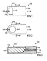
- FIG. 1 illustrates embodiments of a linear electron source 100.
- Fig. 1 shows a schematic cross-sectional view.
- the linear electron source 100 includes a housing 112 which acts as the anode of the electron source.
- the front portion 113 of the housing 112 has an opening 114, for example a slit-opening.
- a cathode 110 is provided within the housing 112 . Electrons that are generated in the housing and which are accelerated towards the front portion 113 of the housing 112 can exit the linear electron source 100 through the opening 114.
- the anode can, for example, be manufactured from a material like copper, aluminum, steel, and mixtures thereof, and the like.
- the linear electron source can be mounted within a vacuum chamber.
- the region exterior of the housing 112 and, in particular, the region between the opening 114 of the electron source and the target for impingement of the electrons can be evacuated to a pressure of, for example, 10 -2 to 10 -4 mbar.
- the linear electron source 100 is connected to a gas supply having a gas conduit 130.
- the flow of gas can be regulated such that the pressure within the housing corresponds to a pressure above 10 -3 , typically a pressure above 10 -2 mbar.
- the gas which is inserted in the housing 112 through the gas conduit 130 can be a gas at least from the group consisting of noble gases, e.g., argon, N 2 , O 2, and mixtures thereof.
- the cathode 110 is connected to a power supply by an electrical conduit or conductor 120.
- the electrical conductor passes through an isolating cathode support member 122.
- the isolating cathode support member 122 is also provided in a gas sealing manner such that the pressure difference from the interior of the housing 112 and the exterior of the housing 112 can be maintained.
- the housing 112 is grounded and acts as an anode. Thereby, the voltage between the cathode 110 and the anode results in generation of a plasma. Electrons generated in the plasma are accelerated towards the anode. Electrons being accelerated towards the front portion 113 can exit the linear electron source 100 through the opening 114.
- the power supply for providing a voltage to the cathode 110 is adapted for controllably providing a voltage in a range of for example -5 kV to -30 kV, typically in a range of -5 kV to -14 kV.
- Fig. 1 shows a cross-sectional view wherein the cathode 110 has a rectangular shape and is mounted within the housing 112 such that a separation space at the bottom, at the top and at the left side is provided. These separation spaces, i.e. the separation spaces which do not face the front surface 113 of the linear electron source 100 can be formed to be substantially uniform.
- the separation space is chosen to be sufficiently large to prevent arcing and sufficiently small to substantially prevent gas discharge between the cathode and the upper, lower and left (see Fig. 1 ) walls of the housing 112.
- the energy distribution of the emitted linear electron beam can be controlled by the potential of the cathode and the pressure within the housing 112.
- the potential of the cathode and the pressure within the housing 112. thereby, for a relatively thick cathode sheath and a relatively thin plasma region a plurality of different energies can be generated depending on the position of the electron generation in the cathode sheath.
- the thin plasma region reduces the probability of energy dissipation within the plasma region. Contrary thereto if the thickness of the plasma region is increased there is an increasing likelihood that the electrons generated in the cathode sheath interact with electrons and ions in the plasma region.
- the energy distribution can typically be below 50%, 30% or 10% of the maximum electron energy. For example, values below 1000 eV such as 100 or 10 eV can be generated. It will be apparent for a person of ordinary skill in the art that the above mentioned values for an energy distribution width will also have a minimum value, which is given by a theoretical minimum, and which might be in a range of 0.1 to 1 eV.
- a linear electron source may also have a cylindrical cathode 210 and a housing 212 which is U-shaped in a cross-sectional view.
- a substantially uniform separation space between the cathode 210 and the anode can be provided.
- a rectangular cathode can typically be used.
- the initial velocity of the generated electrons is better directed towards the front surface 113 (as compared to 213) and, in particular, the opening 114 (as compared to the opening 214).
- a further modification shown in Fig. 2 which can be combined with other embodiments described herein, is that two gas conduits 130 are provided for introducing gas into the housing 212.
- a gas like, for example noble gases, e.g., argon, N 2 , O 2 , or the like can be introduced from an upper portion and a lower portion of the housing 212. This can improve the gas uniformity within the housing 212.
- a more uniform gas distribution in the housing and, in particular in the vicinity of the cathode surface facing the exit slit 214 improves the uniformity of electron generation of the linear electron source 200.
- the cathode support member 122 which also provides the electrical feedthrough for the high voltage for the cathode, can be provided such that the high voltage connection does not necessarily have to be adapted for isolating the high voltage under a reduced atmospheric pressure.
- Fig. 3 shows a side view of a linear electron source 100 from the side facing the opening 114.
- the linear electron source 100 includes a housing 112 acting as an anode, which can typically be grounded, and a cathode 110.
- the front portion 113 is covered by a cover having a slit shaped opening 114.
- the housing 112 has a sidewall 312 at both ends.
- the linear electron source has a length, i.e. from the left sidewall 312 to the right sidewall 312 of 60 cm, 70 cm, 80 cm or larger.
- the length can be at least 70 cm, such as e.g. between 1.5 m to 3 m, for example, 2 m, 2.5 m or 2.8 m.
- the increased length of the linear electron source enables the use of the linear electron source in manufacturing processes that require a high throughout and use, for example, large area substrates, wide webs, sheets or other targets that require electron bombardment over a wide length.
- the length of the cathode 110 is also increased.
- the cathode 110 having an increased length gets longer in light of the thermal expansion coefficient of the cathode material.
- the cathode 110 and the housing 112 typically has a uniform separation space at those opposing surfaces, which are not facing the slit opening 114.
- the cathode can heat up to several hundred degrees Celsius which results in a significant elongation of the cathode with respect to the length thereof.
- the separation space between the cathode and the respective two sidewalls changes during heating up of the cathode.
- the length of the cathode in a cold, i.e. room temperature, state can be such that the separation space between the cathode 110 and the sidewall 312 is a few millimeters larger than it is supposed to be during operation.
- the cathode in a cold state can be about 0.5 mm up to 10 mm too short for the desired separation space preventing glow discharge between the cathode and the housing sidewall being on anode potential.
- the cathode length in a cold state being shorter or, in other words, the separation space from the side of the cathode to the sidewall of the housing being larger than desired during operation, allows for thermal expansion of the cathode during start-up of the operation.
- the cathode can include a material selected from the group consisting of: steel, stainless steel, copper, aluminium, graphite, CFC (carbon-fiber-reinforced carbon), composites thereof, or mixtures thereof.
- the cathode is, for example, manufactured from copper, has a length of 2 m and has a fixed cathode support in the middle thereof, i.e. the cathode extends 1 m to the left and 1 m to the right from a fixed support, the elongation based on the thermal expansion coefficient of 17-10 -6 1/K can be about 8.5 mm on each side.
- the same geometry manufactured from a stainless steel cathode may have an elongation in a range of 2.5 mm to 7.5 mm depending on the type of stainless steel used.
- the same geometry manufactured from a graphite or CFC material cathode might have an elongation in a range of 0.75 mm to 1.5 mm.
- the elongation and, thereby, the additional separation space in a cold status can be reduced for cathode materials like certain stainless steel types, graphite, or CFC.
- Fig. 4 illustrates further embodiments.
- the linear electron source shown in Fig. 4 includes the housing 112, the front portion 113 having the slit opening 114 and the housing sidewall 312, which is only partly shown in order to show the cathode 110 within the housing 112.
- the housing 112 can be grounded to act as an anode of the linear electron source.
- the length L of, for example, 1 m to 3 m, typically 2 m or other values disclosed herein, is indicated by the arrow L.
- Fig. 4 shows only a portion of the linear electron source.
- two or more gas conduits 130 are provided for introducing the gas in the housing 112.
- the two or more gas conduits 130 can be provided on a top side and a bottom side.
- the distance between the individual gas conduits 130 can be in a range of 150 to 300 mm, typically 200 to 250 mm.
- the gas conduits 130 which are connected to a gas tank for providing the desired gas like noble gases, e.g., argon, N 2 , O 2 , mixtures thereof, or the like, have a similar length and arrangement. That is, a cascade of gas conduits is provided, wherein the individual components from the gas tank to the gas inlet in the housing is substantially similar for each of the gas conduits 130. This allows for a uniform pressure for each of the gas inlets in the housing and an electron beam generation with improved uniformity.
- noble gases e.g., argon, N 2 , O 2 , mixtures thereof, or the like
- the first portion from the gas tank to the valve and the second portion from the valve to the gas conduit can have a similar length for each of the gas inlets.
- a small deviation in the individual gas conduits might be acceptable.
- one or more of the elements of a gas conduit, a valve, a tank, and the like can be used in a gas supply for supplying a gas like noble gases, e.g., argon, N 2 , O 2 , mixtures thereof, or the like into the housing of the source.
- At least two gas supplies or even at least 7 gas supplies can be provided.
- the two or more gas supplies may typically share components like the gas tank, gas conduits from the tank to a gas distributor, and/ or valves.
- the cathode 110 has several sides.
- the cathode has a front side 413 and an outer side 412. Further, the cathode 110 has an upper side 414, a lower side 414, and a back side 414.
- the front side 413 has a distance D from the slit opening 114.
- the sides 414 are spaced from the housing 112 by separation spaces. According to some embodiments, which can be combined with other embodiments described herein, the separations spaces between the sides 414 and the housing 112 are substantially similar and e.g. in the range of 3 mm to 7 mm, e.g., 5 mm.
- the sides 412 at each of the ends of the linear electron source have further separation spaces between the -side 412 and the side wall 312 of the housing 112.
- the further separation spaces can, in an operational state, be in the range of 3 mm to 7 mm, e.g., 5 mm, and/or substantially similar to the separation spaces between the sides 414 and the housing 112.
- the further separation space in a non-operational state is between 1 to 10 mm, typically 2 mm, 5 mm or 7 mm larger than in an operations state.
- the sides 413 and 414 can be understood as those sides being parallel to the wall of the housing or the slit opening 114.
- the linear electron source has a length L, which is sufficiently long to provide a long linear electron beam for large area substrates, large webs or sheets, or other wide areas for modem fast production apparatuses.
- the length is typically between 0.7 m and 3 m, e.g. 2 m or 2.5 m.
- the distance D between the slit opening and the front side 413 of the cathode (along the optical axis or optical plane of the source) is typically in a range of 1 cm to 11 cm, for example, 2 cm to 5 cm.
- the length of the linear electron source is at least 5 times or even at least 10 times the distance D from the front cathode side 413 to the opening 114.
- FIG. 5 illustrates further embodiments, which can be combined with other embodiments described herein.
- a linear electron source shown in Fig. 5 includes the housing 112 having the sidewall 312.
- Fig. 5 shows a perspective view from the backside, i.e. the side opposing the slit opening.
- At the backside of the housing 112 different types of support members for supporting the cathode are shown.
- a linear electron source has one fixed cathode support member and one or more floating support members.
- Fig. 5 shows a centre cathode support member 122 with a feedthrough through which the electrical conduit or conductor 120 for providing the high voltage to cathode can be fed.
- a slit opening 524 is provided at both ends of the back surface of the housing.
- a floating support member 522 which is fixed to the cathode for supporting the cathode, can slide within the slit opening 524.
- a sealing member 526 is shown. The sealing member 526 seals the slit opening 524 such that the pressure difference from the interior of the housing 112 and the exterior of the housing 112 can be maintained as desired.
- one fixed support member and two or more floating support members can be provided.
- more than one fixed support member and more than two support members, for example four floating support members can be provided.
- the length of the slit opening 524 can be in a range of 0.5 to 10 mm.
- the length of a slit opening 524 depends on the length of the cathode and the cathode material.
- the thermal extension coefficient may very significantly depending on the cathode material utilized. For example, if a cathode having a length of 2 m is provided and the cathode is fixedly supported in the middle of the cathode, a thermal expansion corresponding to 1 m may occur on each side.
- the slit opening 524 may have a length of 7 to 10 mm, for example 8.5 mm.
- the length of the slit opening 524 may for example be in a range of 3 mm to 8 mm. This value may also depend on the type of stainless steel utilized. If graphite or CFC is used as a cathode material, the length of the slit opening 524 may be reduced to about 0.5 to 2 mm.
- Fig. 6 and 7 Further modifications, which may alternatively or additionally be provided for embodiments, are shown in Fig. 6 and 7 .
- the cathode is supported by support members 622.
- These support members are provided between a lower and a upper surface of the housing 112.
- the support members 622 can be manufactured from an isolation material which does not influence the plasma generation between the cathode 110 and the anode.
- the support members 622 can be floating support members, which can slide in slit opening 724.
- a seal might additionally be provided.
- the slit opening 724 may be a recess in the inner portion of the housing such that no seal is required.
- alternatively or additionally fixed support members without a floating ability can be provided for a lower and upper support member 622.
- the gas supply having the gas conduit 630 may additionally have a gas distribution space 631.
- the gas is provided through the gas conduit 630 in the gas distribution space 631 and small openings or a small slit is provided between the gas distribution space 631 and the interior of the housing 112.
- the inlet for supplying the gas in the housing 112 can be openings 632 with a diameter of 0.5 to 1.5 mm having a distance in the direction of the length of the linear electron source of 5 mm to 10 mm.
- the gas distribution area 631 or gas distribution space provides a uniform gas distribution along the length of the linear electron source, such that a similar pressure is provided at each of the openings 632.
- the openings acting as an inlet for the gas in the housing 112 are provided offset from the gas conduit 630. This might prevent a direct gas flow from the conduit through the openings, whereby the effect of the gas distribution area or space 631 might be improved.
- the individual gas conduits 630 which might be provided along the length of the linear electron source with a distance of 200 to 300 mm or even 500 mm (in the case of a gas distribution area 631) are arranged such that a cascade gas supply module is provided.
- each of the gas conduits, valves, and the like have similar lengths from the gas tank up to the gas distribution area 631.
- Fig. 8 is a cross-sectional view of a linear electron source. Thereby, the cross section is taken at a position without the electrical conduit 120 and at a position without an opening 632 (see Fig. 6 ).
- the cathode 810 may have a core 814 and an outer layer 812.
- the core or main body 814 can be of a material like stainless steel, copper, aluminium or mixtures thereof.
- the outer layer 812 can be, for example of material like graphite or CFC. Providing an outer layer of CFC might reduce the sputtering or removal of cathode material that might occur in light of ions impinging on the cathode.
- a similar effect might be realized by a cathode 910, which is shown in Fig. 9 .
- a body 914 is provided and a front plate 912 is provided at the body.
- the main body 914 includes a material like stainless steel, aluminium, copper and mixtures thereof.
- the front plate might include a material like graphite or CFC.
- the opening 1014 may have an electron emission grid 1015, which is mounted in a recess.
- a grid mounting frame 1016 can be used for mounting the electron emission grid inside the housing 112.
- the distance between the emission grid being on ground potential and the front portion or surface 113 being on ground potential can be adjusted such that the distance between the cathode and the emission grid 1015 is smaller than the distance between a cathode 110 and the front surface 113.
- the electrical field strength might be provided such that a higher electrical field strength is provided in the vicinity of the emission grid.
- the electron emission grid 1015 might be a mash of a material like tungsten or the like. Thereby, a high transparency for having electron trespassing there through can be provided.
- the cathode 110 has several sides.
- the cathode has a front side 413. Another side, which has been described with respect to Fig. 4 , is not shown in the cross-sectional view of Fig. 10 .
- the cathode 110 has an upper side 414, a lower side 414, and a back side 414.
- the front side 413 has a distance D from the slit opening 1014, that is the opening in the front wall 113 of the housing 112.
- the sides 414 are spaced from the housing 112 by separation spaces. According to some embodiments, which can be combined with other embodiments described herein, the separation spaces between the sides 414 and the housing 112 are substantially similar and e.g. in the range of 3 mm to 7 mm, e.g., 5 mm.
- the sides 413 and 414 can be understood as those sides being parallel to the wall of the housing or the slit opening 114.
- the linear electron source has a length, which is sufficiently long to provide a long linear electron beam for large area substrates, large webs or sheets, or other wide areas for modem fast production apparatuses.
- the length is typically between 0.7 m and 3 m, e.g. 2 m or 2.5 m.
- the distance D between the slit opening and the front side 413 of the cathode (along the optical axis or optical plane of the source) is typically in a range of 1 cm to 11 cm, for example 2 cm to 5 cm.
- the length of the linear electron source is at least 5 times or even at least 10 times the distance D from the front cathode side 413 to the opening 114.
- Fig. 11 The corresponding dimensions can also be seen in Fig. 11 .
- the front surface (see, e.g. 113 in Fig. 10 ) can be omitted.
- the opening 1114 can be enlarged such that more electrons may leave the linear electron source.
- the distance D between the front side of the cathode 110 and the opening 1114 can be defined as the distance between the cathode surface and the end of the housing 112, which defines the enlarged opening 1114.
- the intensity of the emitted electron beam can be increased. This might, for example be utilized if the vertical width of the electron beam does not need to be adjusted by a slit opening.
- adjusting plates 1213 can be provided along the opening 1214.
- the adjusting plates 1213 provide an adjustable slit opening 1214. Thereby, the plates 1213 can be mounted for sliding movement towards and away from one another.
- a shutter 1250 can be provided for closing the slit opening 1214 such that no electrons can impinge on the target 10.
- the shutter can be rotatable mounted at a lower portion of the linear electron source. If the shutter 1250 is rotated upwardly, the opening 1214 is closed. If the shutter 1250 is lowered, the electron beam generated inside the chamber 112 can impinge on the target 10.
- Fig. 12 shows a shutter 1250 having two portions. A centre portion covering the majority of the slit 1214 (insert 1252 as the centre portion) and an edge portion 1254.
- the edge portion 1254 is slightly longer than the centre portion 1252. Thereby, the edge portion 1254 covers the outer 1 to 3 cm of the linear electron source.
- the slit opening 1214 can be opened in a centre region of the linear electron source and the outer 1 to 3 cm of the slit opening can still be covered.
- a centre portion of the electron beam can pass towards the target, whereas the outer portion of the electron beam, which might, for example, not be completely uniform, can be blocked.
- the linear electron beam can be focused by a magnetic or electrostatic field.
- the focusing should be conducted in the form of a cylinder lens.
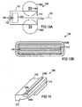
- Fig. 13A and 13B show a linear electron source 100 and a coil 1360 provided around the housing 112 of the linear electron source.
- the coil 1360 provides a magnetic field as indicated by arrows 1362.
- a focusing of the linear electron beam towards a horizontal centre axis or an optical axis 102 can be provided.
- the magnetic field from the coil 1360 may, according to some embodiments, additionally be guided by pole pieces.
- the magnetic field 1362 results in a trajectory of the electron beam, which is rotating around an optical axis 102.
- This rotating trajectory is focused towards the optical axis 102, similarly as a magnetic tens in an electron microscope. Even though, as shown in Fig. 13B , the coil 1360 is not rotational symmetric, a focusing property can be obtained at each position along the length of the linear electron source.
- a similar magnetic field 1462 can be provided by a pair of permanent magnets 1460, which are illustrated in Fig. 14 .
- the magnets 1460 extends along the length of the linear electron source.
- the dash line 1464 is provided for illustrating purposes and separates the north pole from the south pole of the permanent magnet
- electrostatic upper and lower electrodes might be provided in the housing wall or inside the housing for providing a cylindrical length.
- the linear electron source 100 has a cathode 110, and an anode provided by the housing 112 having a slit opening 114 provided in the front face of the linear electron source 100.
- a high voltage can be provided to the cathode by the electrical connection 120.
- the housing is grounded to provide the anode on a ground potential.
- a gas like noble gases e.g., argon, N 2 , O 2 , mixtures thereof or the like is provided from the gas tank 70 through valves 72, 73, gas conduits 130, and gas distribution spaces 631 into the housing 112 for generating a plasma.
- one or more of the elements of a gas conduit, a valve, a gas tank, a gas distribution space , and the like can be used in a gas supply for supplying a gas like noble gases, e.g., argon, N 2 , O 2 , mixtures thereof or the like into the housing of the source.
- a gas like noble gases e.g., argon, N 2 , O 2 , mixtures thereof or the like
- at least two gas supplies or even at least 7 gas supplies can be provided.
- the two or more gas supplies may typically share components like the gas tank, gas conduits from the tank to a gas distributor, and/ or valves.
- the gas conduit 130 providing the gas to the upper gas distribution space 631 has a similar length as the gas conduit 130 providing a gas to the lower gas distribution area 631. Thereby a uniform gas pressure in the housing can be generated. The same applies for different gas inlets provided at the upper, and/or lower portion of the housing along the length of the linear electron source 100.
- valves 72 and 73 are provided for controlling the gas flow in the plasma region.
- the valves are controlled by controller 90 as indicated by arrows 74 and 75, respectively.
- the valves 72 and 73 respectively can be controlled with a reaction time in a range of 1 to 10 msec. Thereby, for example in the case of arcing occurring between the cathode and the anode a fast reaction can be realized.
- the current and thereby the electron beam intensity can be controlled by the amount of gas provided in the plasma region.
- the current provided to the linear electron source is proportional to the current provided by the emission of electrons. For example, if the current should be reduced the valves 72 and 73 are controlled such that the amount of gas in the plasma region is increased.
- the high voltage for a cathode 110 is provided by the power supply 80.
- the controller 90 measures the current provided from the constant voltage source 80 to the cathode. This is indicated by arrow 95 in Fig. 15 .
- the voltage supply 80 can include an arcing rejection control. If arcing occurs between the cathode and the anode the current might show a rapid increase which can be detected by the arcing rejection means of the power supply 80.
- the voltage supply is adapted for switching off and on in a millisecond range, for example 1 msec to 10 msec. Generally, the reaction time might dependent on the velocity a substrate being moved along the electron source.
- the reaction time might even be faster or can be lower if the substrate is not moved or only slowly moved.
- the power supply 80 can be immediately switched of and further switched on again immediately after the arcing disappears.
- this allows for stable operation of the linear electron source.
- the operation can be quasi-continuous. This is in particular relevant if the linear electron source is used for applications for which a target is a fast moving web, foil and the like.
- a main control unit 92 which may have a display means 91 and an input means 93 like a keyboard, a mouse, a touch screen, or the like provides desired values for the current and the voltage.
- the desired current i.e. the electron beam intensity is provided to the controller as indicated by arrow 94.
- the controller measures the present current and adjusts the gas flow in the event the present current is not equal to the desired current.
- the main control unit 92 further gives a desired value for a voltage to the power supply 80 as indicated by arrow 84 in Fig. 15 .
- the voltage provided between the cathode and the anode can be used to influence the energy of the emitted electrons.
- the power supply 80 sets the cathode 110 on a constant potential in a range of -3 to -30, typically -5 to -10 kV, for example -10 kV. Since the anode is grounded, a constant voltage between the cathode and the anode is applied.
- linear electron sources as described above can be used.
- linear electron sources with a length of for example 20 to 60 cm can be used.
- the linear electron sources have a cathode to which a high voltage is provided by an electrical connection and an anode, which is provided by the housing of the linear electron source.
- the emitted electron beam has a uniformity along the length of the linear electron source with a deviation of ⁇ 10% or lower or ⁇ 5% or lower.
- the energy of the electrons in the linear electron beam can be adapted for different applications and the intensity of the linear electron beam can be adapted for different applications.
- a linear electron source and, in particular, a linear electron source according to embodiments described above can be used for charging a foil or a web.
- thick foils or web with a thickness of typically 10 ⁇ m or 25 ⁇ m can be charged with a linear electron source.
- a foil 1622 is guided over a roller 1620.
- Such guiding or transport of a foil 1622 over a roller 1620 can be used in a plurality of apparatuses for manufacturing webs or foils, for deposition material on webs or foils, for patterning thin-film layers on webs or foils, or the like. Thereby, a charge should be provided to the foil for a plurality of reasons.
- the roller 1620 can be charged to a positive potential and a foil or the like can be negatively charged to improve the adhesion of the foil to the roller.
- the foil may be charged by different processes and the charge on the foil should be removed.
- a surface charge on the foil may often not lead to the desirable result.
- a linear electron source 100 is be used for implantation of electrons into the foil.
- an implantation depth of several ⁇ m, for example 2 ⁇ m to 10 ⁇ m can be realized depending on the energy of the electrons 1612 emitted by the linear electron source 100.
- the implantation depth can be adjusted to be at least 20 % of the foil thickness and/or between 50 % and 80 % of the foil thickness. Thereby the charge can be located close to the counter electrode without having significant portions of the charged passing through the foil and impinging on the counter electrode.
- a voltage in a range of -5 to -10 kV or even up to -20 kV, e.g., -15 kV can be applied to the cathode of the linear electron source 100.
- electrons 1612 and ions 1614 are generated.
- the electrons are accelerated towards the front surface of the linear electron source and can exit the linear electron source through the opening 114 for impingement on the foil 1622.
- a slit width of the opening 114 can be provided in a range from 1 mm to 10 mm.
- the emitted current can be limited to be in a range from 10% to 30% of the current provided by the power supply.
- the implantation depth is chosen depending on the thickness of the foil i.e. the implantation depth should be smaller than the thickness of the foil.
- the reaction time of the control of the valves for gas insertion and the reaction time for arc reaction of the power supply can be in the range of a few milliseconds, typically 1 msec to 20 msec.
- methods of electron implantation, methods of heating, or methods of cleaning can provide a distance from the opening 114 or 1714 (see Fig. 17 ) to the target for electron bombardment of 50 mm or below, or of 10 mm or below.
- the scattering rate can be adapted to have at least 80 % or 90 % of the electrons emitted from the opening impinging on the target.
- methods of electron implantation, methods of heating, or methods of cleaning can provide an opening 1714 having a height, which corresponds to at least 50 %, at least 80 %, at least 90 % or even substantially 100 % of the height of the housing.
- the height is defined in a plane perpendicular to the length of the electron source.
- the length of the electron source can be defined as extending in the direction of the slit opening 114 or 1714. Accordingly, for example, in Figs. 16 and 17 the height of the opening is the vertical dimension of the opening.
- the distance between the opening 114 or 1714 and the target for electron bombardment is below 5 mm. Thereby, essentially all electrons, which do not hit the anode, will be guided on the target.
- a further method according to an example usefull for understanding the invention using a linear electron source in general or linear electron sources as described herein can be the heating and/or cleaning of metal foils.
- Metal foils are, for example used for the manufacturing of photovoltaic thin films. During manufacturing of thin-film solar cells or other films for which metal foils are used, the metal foil needs to be preheated for various processing steps.
- Fig. 17 shows a linear electron source 1700, which is positioned in front of a metal foil 1722 guided over a roller 1720.
- the cathode 1710 of the linear electron source 1700 can be increased in size.
- the surface of the cathode can have an area in a range of 50 to 6000 cm 2 .
- the height of the cathode i.e. the vertical direction in Fig. 17 , can be in a range of 1 cm to 30 cm.
- the height can, in particular, be in a range of 15 cm to 30 cm, for example, 15 cm or 20 cm.
- the intensity of the emitted linear electron beam should be increased.
- the enlarged cathode surface results in increased electron beam intensity, that is, in an increased electron beam current.
- the opening 1714 of the linear electron source 1700 is provided to be at least 80 or 90% of the height of the housing.
- a front surface for providing a slit opening can be omitted. Thereby, the electron beam current can be further increased.
- the distance from the linear electron source 1700 to the foil 1722 can be reduced to be below 50 mm. Thereby all electrons being emitted from the wide opening can impinge on the foil.
- the efficiency of providing power into intensity on a metal foil can be improved by increasing the front surface of the cathode 1710, by providing a wide opening 1714, which may substantially correspond to the dimensions of the housing of the linear electron source and/or by reducing the distance of the linear electron source 1700 to the target.
- the wide electron beam opening can provide an efficiency of up to 80%.
- Typical voltages between the cathode and the anode can be in a range of 5 to 10 kV. Further it is also possible to provide higher voltages in a range of 12 to 15 kV, for example 13 kV.
- the methods of heating a metal foil can also be used for cleaning of a metal foil. Thereby, disposals of oil or other materials which adhere to the metal foil can be evaporated by heating the metal foil. Further, complex chemical components, for example, oils can be cracked by the energy provided with the electron beam. The crack remainders of the oil and the like can then be removed by evaporation.
- Linear electron sources as described herein can be used for removal of oil from a web foil.
- Capacitors for example can be produced on a web foil by providing a pattern of oil on the foil and depositing metal films in the region which is not covered by oil. Thereby, after the metal deposition process, the oil needs to be removed and even small remainders of oil on the web may deteriorate the operation of the capacitors to be manufactured. Thus, it is desirable, to have a fast process to remove oil from a web even if the web velocity is high during the manufacturing process. According to embodiments described herein, the oil from a web can be removed by a method described with regard to Fig. 17 .
- Fig. 17 shows a linear electron source 1700, which is positioned in front of a metal foil 1722 guided over a roller 1720.
- the cathode 1710 of the linear electron source 1700 can be increased in size.
- the surface of the cathode can have an area in a range of 50 to 6000 cm 2 .
- the height of the cathode i.e. the vertical direction in Fig. 17 , can be in a range of 1 cm to 30 cm.
- the height can, in particular, be in a range of 15 cm to 30 cm, for example, 15 cm or 20 cm.
- the intensity of the emitted linear electron beam should be increased.
- the enlarged cathode surface results in increased electron beam intensity, that is the electron beam current.
- the opening 1714 of the linear electron source 1700 is provided to be at least 80 or 90% of the height of the housing.
- a front surface for providing a slit opening can be omitted. Thereby, the electron beam current can be further increased.
- the distance from the linear electron source 1700 to the foil 1722 can be reduced to be below 50 mm. Thereby all electrons being emitted from the wide opening can impinge on the foil.
- the efficiency of providing power into intensity on a metal foil can be improved by increasing the front surface of the cathode 1710, by providing a wide opening 1714, which may substantially correspond to the dimensions of the housing of the linear electron source and/or by reducing the distance of the linear electron source 1700 to the target.
- the wide electron beam opening can provide an efficiency of up to 80%.
- Typical voltages between the cathode and the anode can be in a range of 5 to 10 kV. Further it is also possible to provide higher voltages in a range of 12 to 15 kV, for example 13 kV.
- a linear electron source in general and, in particular, linear electron sources as described herein can be used for an evaporation apparatus.
- an appropriator For thin-film coating of a material on a substrate, an appropriator can be used.
- coatings with metal films which provide a capacitor of a large panel display or a protective layer on a flexible structure or web can be applied with evaporators.
- evaporators there is a tendency, in particular for large panel displays that the substrate size increases and the coating processes need to be improved.
- Fig. 18 shows an evaporator having a linear electron source 100 arranged below an evaporation crucible 180.
- the linear electron source 100 has a housing 112 with a side wall 312 and a slit opening 114.
- a slit opening 114 faces the lower portion of the evaporation crucible 180.
- the electron beam impinges on the lower side of the evaporation crucible 180 and thereby heats the evaporation crucible.
- the aluminium may be fed in a melting area of the evaporation crucible in a recess portion 182. Further, the aluminium is heated such that it is evaporated and can be deposited on a substrate or the like.
- FIG. 19 A further example of an evaporator is shown in Fig. 19 .
- a plurality of evaporation crucibles 980 is positioned above the slit opening 114 of the linear electron source 100.
- the evaporation crucibles 980 can be arranged with respect to each other such that there is no gap between the evaporation crucibles.
- a material to be evaporated can be fed into each of the evaporation crucibles having a recess portion and the crucibles are heated to evaporate the material like aluminium, or the like.
- Fig. 20 shows a linear electron source 100 having a cathode 110 and a housing 112 acting as the anode.
- the cathode 110 is connected to a high voltage source by an electrical connector 120 which is provided through a cathode support member 122.
- a gas like noble gases e.g., argon, N 2 , O 2 , mixtures thereof or the like can be inserted via a gas conduit 130.
- electrons are accelerated toward the target in the form of an evaporation crucible 2080. Thereby, the evaporation crucible is heated such that material to be deposited on a substrate is melted and evaporated.
- the temperature of the crucible can be in a range of 1000 °C to 1600 °C, depending on the material to be evaporated.
- the evaporation crucible 2080 can have a recess portion 2084 for receiving the melted material.
- the material can, for example, be continuously fed to the evaporation crucible by a wire.
- the material for manufacturing the evaporation crucible 2080 can typically be selected from the group consisting of a metallic boride, a metallic nitride, a metallic carbide, a non-metallic boride, a non-metallic nitride, a non-metallic carbide, nitrides, borides, graphite, TiB 2 , BN, B 4 C, SiC and combinations thereof. Further, in particular materials like Al 2 O 3 or ceramic materials can be used. According to further embodiments, the compositions described above can be chosen such that the evaporation crucible 2080 has an electrical conductivity corresponding to a resistance of 2000 ⁇ cm and above or of 300 ⁇ cm or below.
- the resistances for crucibles provided herein refer to the resistance in a cold state. Since the evaporation crucible is not heated by a current fed there through, the choice of material for the evaporation crucible is significantly increased and the materials can be chosen independent of the electric properties of the crucible.
- the evaporation crucible 2080 is located on thermal isolating members 2086. These support members do not need to be of an electrical conductor. Thus, the choice of material can be adapted for thermal isolation. According to different embodiments, materials like high-temperature metals, high temperature ceramics, or the like can be used. Further, the cross-section area at which the crucible is in contact with the support member can be reduced to 2 mm 2 to 10 mm 2 according to some further embodiments. Thereby, the support member for the evaporation crucible 2080 results in a reduced heat capacitance of the combination of the crucible and the support thereof. The reduced heat capacitance results in the necessity for reduced energy transfer to the crucible in order to provide the desired temperatures. For example, the crucible support can have a thermal conductivity of 100 (W/m ⁇ K) or lower, or even 10 (W/m ⁇ K) or lower.
- a plasma electron source in general and, in particular, the linear electron source according to embodiments described herein can be used for heating of a silicon wafer.
- processes during semiconductor manufacturing for which silicon wafers need to be heated can be deposition processes, annealing processes or other processes for which an elevated wafer temperature should be used.
- Many semiconductor processing apparatuses use electromagnetic radiation, for example in the form of infrared radiation for heating of a silicon wafer.
- these heating processes suffer from the absorption of infrared radiation in the silicon material.
- many radiation sources have a relatively wide emission angle. Thus, a lot of energy does riot reach the area of the silicon wafer to be heated.
- a plasma electron source 100 can be arranged such that a surface of a silicon wafer 2102 is eradiated by an electron beam.
- the plasma electron source includes a cathode 110 to which a high voltage is applied through an electrical conduit 120.
- the housing 112 acts as an anode and, for example, can be grounded. Gases like noble gases, e.g., argon, N 2 , O 2 , mixtures thereof or the like are inserted through gas conduit 130 to provide a uniform gas pressure in the area of the cathode 110. Due to the voltage between the cathode 110 and the anode provided by the housing 112 a plasma is generated. Thereby, electrons are generated.
- the silicon wafer 2102 is located on a support 2186 such that one surface of the wafer can be provided with electron bombardment. Typically the electron impinges on the backside of the silicon wafer, that is, the side of the silicon wafer, on which the wafer is not processed.
- the opening for the exit of the electron beam is at least of a size corresponding to the cathode 110, at least of a size corresponding to 80 or 90% of the respective dimension of the housing 112, or of a size corresponding to the size of the housing 112, whereby a front surface (see, e.g., 113 in Fig. 1 ) can be omitted.
- the plasma electron source can be a linear plasma electron source, preferably of a length above 60 cm.
- a linear plasma electron source can be a source according to embodiments described herein.
- the current reaching the target that is, a silicon wafer
- cathode voltages in a range of -5 to -8 kV.
- the electron beam from the plasma electron source and, in particular a linear plasma electron source can provide an efficient energy transfer or charge transfer since the electron beam can be well directed towards the desired target. According to embodiments described herein it is possible that at least 60%, for example, 70 or 80% of the energy provided to the source is transferred to the target.
- the electrons provide the energy directly to the silicon wafer.
- the absorption of the energy in the silicon wafer is improved as compared to the absorption of electromagnetic radiation. Accordingly, the energy, which is provided at the wafer surface, can be reduced for generating the desired temperature
- a linear plasma electron source can be provided.
- the source includes a housing acting as a first electrode, the housing having side walls, a slit opening in the housing for trespassing of an electron beam, the slit opening defining a length direction of the source, a second electrode being arranged within the housing and having a first side facing the slit opening, the first side being spaced from the slit opening by a first distance, wherein the length of the electron source in the length direction is at least 5 times the first distance, and at least one gas supply for providing a gas into the housing, wherein the first electrode is the anode and the second electrode is the cathode.
- the linear plasma electron source may have the length of the electron source in the length direction being at least 20 times the first distance.
- the second electrode can have second further sides facing the side walls, and third further sides, wherein the side of the second electrode is spaced from the slit opening by a first distance (D), wherein the second further side of the second electrode and the third further sides being spaced from the housing by separation spaces being smaller than the first distance, and wherein the separation space between the second further side and the side wall is adapted for increasing from a non-operational state to an operational state by at least 1 mm.
- the length of the housing in the length directions can be at least 1.5 m.
- the second electrode can include at least a material selected from the group consisting of: stainless steel, graphite, and CFC.
- the source can further include a first support member for supporting the second electrode at a fixed position with respect to the housing; and at least one second support member for supporting the second electrode at a floating position with respect to the housing.
- the second support member can be floating in an opening in the housing.
- the second electrode can include at least a material selected from the group consisting of: stainless steel and copper, and wherein the opening has a floating length extending in the length direction of at least 3 mm or the second electrode can include at least a material selected from the group consisting of: graphite and CFC, and wherein the opening has a floating length extending in the length direction of at least 1 mm.
- the opening in the housing can be a slit opening for floating movement of the at least one second support member with a floating length of at least 1 mm.
- the source includes at least one seal for reducing the gas flow in the opening for floating movement of the at least one second support member.
- the at least one second support member can be at least two second support members.
- the second electrode can be connected to a power supply for providing a high voltage to the second electrode.
- the second electrode and a power supply can be connected with an electrical connections being arranged through the fixed support member.
- the second electrode can be a rectangular cross-section.
- the at least one gas supply can be a plurality of gas supplies with a distance along the length direction of at least 200 mm.
- the at least one gas supply may include a gas conduit for the at least one gas supply; and a gas distribution area or space in communication with the gas conduit and adjacent to the housing for improving the uniformity of the gas pressure along the length direction.
- a wall separating the gas distribution space and the housing can have a plurality of openings for insertion of the gas in the housing.
- the linear plasma electron source may further include further support members supporting the second electrode at the third further sides.
- the further support members can be adapted for floating movement with respect to the housing.
- the second electrode can have a main body and an outer layer.
- the main body can include at least a material selected from the group consisting of: stainless steel, aluminum, copper, and mixtures thereof; and the outer layer includes at least a material selected from the group consisting of: graphite, CFC, and mixtures thereof.
- the outer layer can encircle the main body or the outer layer can be provided at the first side of the second electrode.
- the source may further include a charged particle emission grid being recessed from the slit opening towards the inside of the housing.
- the slit opening can have a height, that is, a direction perpendicular to the length direction, being at least 50 % of the height of the housing.
- the height of the slit opening can correspond essentially to the height of the housing.
- the source may include at least one slit height adjusting plate and/or a movable shutter for selectively blocking the charged particle beam.
- the first side of the second electrode can have a height, that is a dimension perpendicular to the length direction, being at least 1 to 30 cm or even 15 to 30 cm.
- the focusing lens can include a coil wound around the housing, a permanent magnet extending along the length direction, and/or at least two electrodes.
- At least one gas supply can include a plurality gas conduits, and at least one valve, and wherein the plurality of gas conduits are similar to provide a cascade of gas supplies.
- each of the gas supplies can provide a valve.
- the at least one gas supply can be controlled by a controller being adapted for sensing the current supplied to the cathode and having a reaction time of 100 ms or faster, the controller can be connected to a main control unit for receiving a desired current value, the power supply can include an arc rejection with a reaction time of 10 ms or faster, and/or the power supply can be connected to a main control unit for receiving a desired voltage value.
- a method of manufacturing a linear plasma electron source includes manufacturing a housing acting as a first electrode and having a slit opening defining a length direction; providing a second electrode in the housing with a first side adapted for facing the slit opening and being spaced from the slit opening by a first distance, wherein the second electrode has second further sides adapted for facing side walls, and third further sides adapted for facing the housing; defining predetermined separation spaces between the second further side of the second electrode and the housing side alls and the third further sides and the housing; mounting the second electrode in the housing with a length of the second electrode in the length direction being at least 1 mm smaller than the predetermined separation space between the second further side and the housing side wall; and connecting at least one gas supply to the housing.
- the second electrode can be fixedly mounted to the housing at a first position and mounted to the housing with a floating bearing at further positions.
- the first position can be located substantially at the center of the second electrode and/or the housing.
- the method may include sealing the floating bearing and/or providing a sealed electrical connection for the second electrode.
- an evaporation apparatus for evaporating a material to be deposited.
- the evaporation apparatus includes at least one evaporation crucible having a body with an area for receiving the material to be deposited at one side; a linear electron source being positioned adjacent to the evaporation crucible for impingement of an electron beam on another side.
- the linear electron source includes a housing acting as a first electrode, the housing having side walls; a slit opening in the housing for trespassing of a electron beam, the slit opening defining a length direction of the source; a second electrode being arranged within the housing and having a first side facing the slit opening; and at least one gas supply for providing a gas into the housing.
- the material for manufacturing the evaporation crucible body can be selected from the group consisting of: a metallic boride, a metallic nitride, a metallic carbide, a non-metallic boride, a non-metallic nitride, a non-metallic carbide, nitrides, borides, a ceramic material, graphite, TiB2, BN, B4C, SiC, A1203 and combinations thereof.
- the material for manufacturing the evaporation crucible body can have A resistance of 2000 ⁇ cm and above or of 300 ⁇ cm or below.
- the evaporation apparatus can include a crucible support.
- the crucible support can have , a contact area to the crucible of .2 mm 2 to 10 mm 2 , and/or a thermal conductivity of 200 (W/m ⁇ K) or lower.
- a linear electron source according to any of the embodiments described herein can be used for the evaporation apparatus.
- a method of charging a web or foil includes guiding a web or foil having a thickness of 10 ⁇ m or larger with at least one roller; providing a linear electron source having a housing acting as an anode, the housing having side walls; a slit opening in the housing for trespassing of a linear electron beam, the slit opening defining a length direction of the source; a cathode being arranged within the housing and having a first side facing the slit opening; at least one gas supply for providing a gas into the housing; and a power supply for providing a high voltage between the anode and the cathode; and emitting the linear electron beam, wherein the high voltage is adjusted for providing an electron energy to implant electrons of the electron beam within the web or foil.
- the foil or web that may typically have thickness of at least 25 ⁇ m is guided.
- the electrons can be implanted to an implantation depth of at least 20% of the thickness of the foil and/or to an implantation depth is adjusted to be between 40% and 80% of the thickness of the foil.
- the high voltage can be adjusted between -4 kV and -15 kV, the providing of gas can be controlled with a controller having a reaction time of 100 ms or faster, and/or arcing can be detected and the detection of arcing switches the high voltage with a reaction time of 10 ms.
- the height of the slit opening in a direction perpendicular to the length direction can be at least 50 % of the corresponding height of the housing.
- the linear electron source is provided such that the distance between the slit opening and the web or foil can be 20 mm or below.
- the linear electron source in particular for large heights of the slit opening of 50 %, 80 % or even 90 % the height of the housing, it can be possible to position the linear electron source substantially directly at the target to be bombarded with electrons.
- a linear electron source according to any of the embodiments described herein can be used for implanting charge.
- a method of heating or cleaning a web or foil includes providing a linear plasma electron source having a housing acting as an anode, the housing having side walls; a slit opening in the housing for trespassing of an electron beam, the slit opening defining a length direction of the source, a cathode being arranged within the housing and having a first side facing the slit opening; at least one gas supply for providing a gas into the housing; and a power supply for providing a high voltage between the anode and the cathode; guiding the web or foil movably in front of the slit opening; and emitting a linear electron beam from the linear plasma electron source.
- a width of the opening can be at least 50 % or even at least 80 % of corresponding width of the housing.
- at least 20% of the power provided by the power supply can be provided to the web or foil or at least 60% of the power provided by the power supply is provided to the web or foil.
- the web or foil can be a metal foil. Thereby, for example, it is typically possible to move the metal foil being guided by at least one roller along the linear plasma electron source with a velocity of at least 1 cm/min. Further, additionally or alternatively, the power absorption of the electron beam can be used for preheating of the metal foil or the power absorption of the electron beam can be used for cleaning the metal foil. For example, the power absorption may crack molecule remainders on the metal foil.
- the web or foil can be a web foil. Thereby, for example, it is typically possible to move the web foil being guided by at least one roller along the plasma electron source with a velocity of at least 1 cm/min. Further, additionally or alternatively, the power absorption of the electron beam is used for cleaning of the web foil. As a typical option, the power absorption of the electron beam can be used for oil removal from the web foil. For example, the power absorption may cracks molecule remainders on the web foil.
- a method of heating a silicon substrate includes providing a plasma electron source having a housing acting as an anode, the housing having side walls; an opening in the housing for trespassing of an electron beam, a cathode being arranged within the housing and having a first side facing the opening; at least one gas supply for providing a gas into the housing; and a power supply for providing a high voltage between the anode and the cathode; providing the silicon substrate in front of the opening; and emitting the electron beam to directly impinge on the silicon wafer.
Landscapes
- Chemical & Material Sciences (AREA)
- Engineering & Computer Science (AREA)
- Organic Chemistry (AREA)
- Materials Engineering (AREA)
- Mechanical Engineering (AREA)
- Metallurgy (AREA)
- Chemical Kinetics & Catalysis (AREA)
- Analytical Chemistry (AREA)
- Health & Medical Sciences (AREA)
- Toxicology (AREA)
- Physics & Mathematics (AREA)
- Plasma & Fusion (AREA)
- Electron Sources, Ion Sources (AREA)
- Physical Or Chemical Processes And Apparatus (AREA)
- Plasma Technology (AREA)
Claims (24)
- Verfahren zum Laden eines Gewebes oder einer Folie, umfassend Führen eines Gewebes oder einer Folie, das bzw. die eine Dicke von 10 µm oder mehr aufweist, mit mindestens einer Rolle;
bereitstellen einer linearen Elektronenquelle (100; 1700), die ein Gehäuse (112; 212; 1012) aufweist, das als Anode dient, wobei das Gehäuse Seitenwände(312) aufweist; eine Schlitzöffnung (114; 1214; 1714; 2114) in dem Gehäuse zum Eindringen des linearen Elektronenstrahls dient, wobei die Schlitzöffnung eine Längsrichtung der Quelle definiert; eine Kathode, die in dem Gehäuse angeordnet ist und eine erste Seite (413) aufweist, die der Schlitzöffnung zugewandt ist; mindestens eine Gaszufuhr (130; 630; 72, 73, 70) zum Bereitstelen von Gas in dem Gehäuse; und eine Energieversorgung (80) zum Bereitstellen einer Hochspannung zwischen der Anode und der Kathode;
Emittieren des linearen Elektronenstrahls, wobei die Hochspannung eingestellt ist, um eine Elektronenenergie bereitzustellen, um Elektronen des Elektronenstrahls in dem Gewebe oder in der Folie zu implantieren. - Verfahren nach Anspruch 1, wobei eine Folie oder Gewebe, die bzw. das eine Dicke von mindestens 25 µm aufweist, geführt wird.
- Verfahren nach einem der Ansprüche 1 bis 2, wobei die Elektronen in einer Implantationstiefe von mindestens 20% der Dicke der Folie implantiert werden.
- Verfahren nach einem der Ansprüche 1 bis 3, wobei die Elektronen in einer Implantationstiefe, die zwischen 40% und 80% der Dicke der Folie eingestellt wird, implantiert werden.
- Verfahren nach einem der Ansprüche 1 bis 4, wobei die Hochspannung zwischen -4 kV und -15 kV eingestellt wird.
- Verfahren nach einem der Ansprüche 1 bis 5, wobei das Bereitstellen von Gas mit einer Steuerung, die eine Reaktionszeit von 100ms oder schneller aufweist, gesteuert wird.
- Verfahren nach einem der Ansprüche 1 bis 6, wobei ein Lichtbogen detektiert wird und das Detektieren von einem Lichtbogen die Hochspannung mit einer Reaktionszeit von 10 ms oder weniger schaltet.
- Verfahren nach einem der Ansprüche 1 bis 7, wobei die Höhe der Schlitzöffnung (114; 1214; 1714; 2114) in einer Richtung orthogonal zu der Längsrichtung mindestens 50% der entsprechenden Höhe des Gehäuses (112; 212; 1012) ist.
- Verfahren nach einem der Ansprüche 1 bis 8, wobei die lineare Elektronenquelle (100; 1700) derart bereitgestellt wird, dass die Entfernung zwischen der Schlitzöffnung (114; 1214; 1714; 2114) und dem Gewebe oder Folie 20 mm oder weniger beträgt.
- Verfahren nach einem der Ansprüche 1 bis 9, wobei die erste Seite (413) von der Schlitzöffnung (114; 1214; 1712; 2114) durch eine erste Entfernung beabstandet ist, wobei die Länge der Elektronenquelle (100; 1700) in die Längsrichtung mindestens 5 Mal der ersten Entfernung oder mindestens 20 Mal der ersten Entfernung beträgt, und wobei die Anode eine erste Elektrode und die Kathode eine zweite Elektrode (110; 210; 810; 910) ist.
- Verfahren nach Anspruch 10, wobei die zweite Elektrode (110; 210; 810; 910) mit zweiten weiteren Seiten (412), die der Seitenwand (312) zugewandt sind , und dritte weitere Seiten (414) bereitgestellt wird, wobei die Seite (413) von der zweiten Elektrode (110; 210; 810; 910) mit einer ersten Entfernung (D) von der Schlitzöffnung (114; 1214; 1714; 2114) beabstandet ist, wobei die zweite weitere Seite der zweiten Elektrode und die dritten weiteren Seiten von dem Gehäuse (112; 212; 1012) durch Trennabstände beabstandet sind, die kleiner als die erste Entfernung sind, und wobei der Trennabstand zwischen der zweiten weiteren Seite und der Seitenwand eingerichtet sind, um sich von einem Nichtbetriebszustand zu einem Betriebszustand um mindestens 1mm zu vergrößern.
- Verfahren nach einem der Ansprüche 10 oder 11, wobei die Länge (L) des Gehäuses (112; 212; 1012) in die Längsrichtungen bereitgestellt wird, um mindestens 1.5 m zu betragen.
- Verfahren nach einem der Ansprüche 10 bis 12, wobei die zweite Elektrode (110; 210; 810; 910) bereitgestellt wird, um mindestens ein Material zu umfassen, das aus der Gruppe ausgewählt wird, bestehend aus: Edelstahl, Graphit, und CFC.
- Verfahren nach einem der Ansprüche 10 bis 13, ferner umfassend Bereitstellen: einer ersten Stützvorrichtung (122; 622), um die zweite Elektrode (110; 210; 810; 910) an einer festen Position in Bezug auf das Gehäuse (112; 212; 1012) zu stützen; und
mindestens einer zweiten Stützvorrichtung (522), um die zweite Elektrode bei einer schwimmende Position in Bezug auf das Gehäuse (112; 212; 1012) zu stützen. - Verfahren nach Anspruch 14, wobei die zweite Stützvorrichtung (522) in einer Öffnung (524) in dem Gehäuse (112; 212; 1012) schwimmt.
- Verfahren nach Anspruch 15, wobei die Öffnung in dem Gehäuse (112; 212; 1012) eine Schlitzöffnung (524; 724) zur schwimmenden Bewegung der mindestens einen zweiten Stützvorrichtung (522) mit einer Schwimmlänge von mindestens 1 mm ist.
- Verfahren nach einem der Ansprüche 15 bis 16, ferner umfassend Bereitstellen:mindestens einer Dichtung (526) zum Vermindern des Gasflusses in die Öffnung zur schwimmenden Bewegung der mindestens einen zweiten Stützvorrichtung (522).
- Verfahren nach einem der Ansprüche 10 bis 17, wobei die zweite Elektrode (110; 810; 910) einen rechteckigen Querschnitt aufweist.
- Verfahren nach einem der Ansprüche 10 bis 18, wobei die mindestens eine Gaszufuhr (70) ferner umfasst:eine Vielzahl von Gasleitungen (130; 630) mit einem Abstand entlang der Längsrichtung von mindestens 200 mm;mindestens einen Gasverteilraum (631) in Verbindung mit der Vielzahl von Gasleitungen und angrenzend an das Gehäuse (112; 212; 1012) zum Verbessern der Gleichmäßigkeit des Gasdrucks entlang der Längsrichtung;mindestens ein Ventil, wobei die Vielzahl von Gasleitungen ähnlich sind, um eine Kaskade von Gaszufuhren bereitzustellen, und wobei eine Wand, die den Gasverteilraum (631) und das Gehäuse (112; 212; 1012) trennt, eine Vielzahl von Öffnungen zum Einführen des Gas in das Gehäuse aufweist.
- Verfahren nach einem der Ansprüche 10 bis 19, wobei die zweite Elektrode (110; 210; 810; 910) mit einem Hauptkörper (814; 914) und einer Außenschicht (812; 912) bereitgestellt wird.
- Verfahren nach Anspruch 20, wobei der Hauptkörper mindestens ein Material umfasst, das aus der Gruppe ausgewählt ist, bestehend aus: Edelstahl, Aluminium, Kupfer, und Mischungen davon; und die Außenschicht (812; 912) umfasst mindestens ein Material ausgewählt von der Gruppe bestehend aus: Graphit, CFC, und Mischungen davon.
- Verfahren nach einem der Ansprüche 10 bis 21, wobei die Breite von der Schlitzöffnung (114; 1214; 1714; 2114) im Wesentlichen der Höhe des Gehäuses (112; 212; 1012) entspricht.
- Verfahren nach einem der Ansprüche 10 bis 22, wobei die erste Seite (413) der zweiten Elektrode (110; 210; 810; 910) mit einer Höhe, das heißt in einer Dimension orthogonal zu der Längsrichtung, bereitgestellt wird, die mindestens 1 bis 30 cm, typischerweise 15 bis 30 cm beträgt.
- Verfahren nach einem der Ansprüche 10 bis 23, ferner bereitstellend:eine Fokussierlinse (1360; 1460) zum Fokussieren des linearen Strahls geladener Teilchen in Richtung der optischen Ebene, die sich durch die Schlitzöffnung (114; 1214; 1714; 2114) erstreckt.
Priority Applications (5)
| Application Number | Priority Date | Filing Date | Title |
|---|---|---|---|
| EP07024960A EP2073249B1 (de) | 2007-12-21 | 2007-12-21 | Lineare Elektronenquelle und deren Anwendung für die Aufladung von Folien |
| CN200880121937.7A CN101903969B (zh) | 2007-12-21 | 2008-11-24 | 线性电子源和使用线性电子源的蒸发器以及电子源的应用 |
| US12/276,872 US7928411B2 (en) | 2007-12-21 | 2008-11-24 | Linear electron source, evaporator using linear electron source, and applications of electron sources |
| TW097145385A TWI405235B (zh) | 2007-12-21 | 2008-11-24 | 充電腹鈑或箔之方法 |
| PCT/EP2008/066096 WO2009080430A1 (en) | 2007-12-21 | 2008-11-24 | Linear electron source, evaporator using linear electron source, and appliccations of electron sources |
Applications Claiming Priority (1)
| Application Number | Priority Date | Filing Date | Title |
|---|---|---|---|
| EP07024960A EP2073249B1 (de) | 2007-12-21 | 2007-12-21 | Lineare Elektronenquelle und deren Anwendung für die Aufladung von Folien |
Publications (2)
| Publication Number | Publication Date |
|---|---|
| EP2073249A1 EP2073249A1 (de) | 2009-06-24 |
| EP2073249B1 true EP2073249B1 (de) | 2012-06-13 |
Family
ID=39709283
Family Applications (1)
| Application Number | Title | Priority Date | Filing Date |
|---|---|---|---|
| EP07024960A Active EP2073249B1 (de) | 2007-12-21 | 2007-12-21 | Lineare Elektronenquelle und deren Anwendung für die Aufladung von Folien |
Country Status (5)
| Country | Link |
|---|---|
| US (1) | US7928411B2 (de) |
| EP (1) | EP2073249B1 (de) |
| CN (1) | CN101903969B (de) |
| TW (1) | TWI405235B (de) |
| WO (1) | WO2009080430A1 (de) |
Families Citing this family (8)
| Publication number | Priority date | Publication date | Assignee | Title |
|---|---|---|---|---|
| US8748773B2 (en) * | 2007-03-30 | 2014-06-10 | Ati Properties, Inc. | Ion plasma electron emitters for a melting furnace |
| EP2073243B1 (de) * | 2007-12-21 | 2018-10-03 | Applied Materials, Inc. | Lineare Elektronenquelle sowie Elektronenstrahlverdampfer mit linearer Elektronenquelle und deren Anwendungen |
| EP2435537A4 (de) | 2009-05-26 | 2013-09-04 | Inentec Llc | Hochdruck-gasifiziersystem unter verwendung elektrisch unterstützter heizung |
| CN107078004B (zh) * | 2014-11-07 | 2019-10-15 | 应用材料公司 | 用于利用电子束处理具有大宽度柔性基板的设备和方法 |
| US9508976B2 (en) | 2015-01-09 | 2016-11-29 | Applied Materials, Inc. | Battery separator with dielectric coating |
| KR102419382B1 (ko) | 2017-08-17 | 2022-07-12 | 어플라이드 머티어리얼스, 인코포레이티드 | 올레핀 분리기가 없는 Li-이온 배터리 |
| WO2020037494A1 (en) | 2018-08-21 | 2020-02-27 | Applied Materials, Inc. | Ultra-thin ceramic coating on separator for batteries |
| DE102019102008A1 (de) | 2019-01-28 | 2020-07-30 | Fraunhofer-Gesellschaft zur Förderung der angewandten Forschung e.V. | Vorrichtung zum Beschichten eines bandförmigen Substrates |
Family Cites Families (15)
| Publication number | Priority date | Publication date | Assignee | Title |
|---|---|---|---|---|
| US5170032A (en) * | 1957-06-27 | 1992-12-08 | Lemelson Jerome H | Radiation manufacturing apparatus and amendment |
| US5039836A (en) * | 1957-06-27 | 1991-08-13 | Lemelson Jerome H | Radiation manufacturing apparatus and method |
| US4842893A (en) * | 1983-12-19 | 1989-06-27 | Spectrum Control, Inc. | High speed process for coating substrates |
| US4647818A (en) * | 1984-04-16 | 1987-03-03 | Sfe Technologies | Nonthermionic hollow anode gas discharge electron beam source |
| US6083628A (en) * | 1994-11-04 | 2000-07-04 | Sigma Laboratories Of Arizona, Inc. | Hybrid polymer film |
| US5909032A (en) * | 1995-01-05 | 1999-06-01 | American International Technologies, Inc. | Apparatus and method for a modular electron beam system for the treatment of surfaces |
| DE19613713C1 (de) * | 1996-03-29 | 1997-08-21 | Fraunhofer Ges Forschung | Verfahren zur Herstellung von Feldemissionselektronenquellen, so hergestellte Feldemissionselektronenquelle und ihre Verwendung |
| JP4052731B2 (ja) * | 1998-06-18 | 2008-02-27 | 株式会社アドバンテスト | 電子銃 |
| RU2200058C1 (ru) * | 2002-02-12 | 2003-03-10 | Открытое акционерное общество "ТВЭЛ" | Способ проведения гомогенных и гетерогенных химических реакций с использованием плазмы |
| TW586133B (en) * | 2002-05-06 | 2004-05-01 | Chunghwa Picture Tubes Ltd | Multi-electron beam mark type cathode ray tube having horizontal fluorescent band |
| JP4216567B2 (ja) * | 2002-11-01 | 2009-01-28 | パナソニック株式会社 | 真空蒸着方法および蒸着装置 |
| US20050208229A1 (en) * | 2003-12-11 | 2005-09-22 | Sumitomo Chemical Company, Limited | Process for producing adhesive film |
| JP2007100162A (ja) * | 2005-10-04 | 2007-04-19 | Tdk Corp | 薄膜形成方法、磁気記録媒体製造方法および薄膜形成装置 |
| EP2073243B1 (de) * | 2007-12-21 | 2018-10-03 | Applied Materials, Inc. | Lineare Elektronenquelle sowie Elektronenstrahlverdampfer mit linearer Elektronenquelle und deren Anwendungen |
| EP2088612A1 (de) * | 2007-12-21 | 2009-08-12 | Applied Materials, Inc. | Verfahren zur Erhitzung oder Reinigung einer Materialbahn oder einer Folie |
-
2007
- 2007-12-21 EP EP07024960A patent/EP2073249B1/de active Active
-
2008
- 2008-11-24 TW TW097145385A patent/TWI405235B/zh active
- 2008-11-24 US US12/276,872 patent/US7928411B2/en active Active
- 2008-11-24 WO PCT/EP2008/066096 patent/WO2009080430A1/en active Application Filing
- 2008-11-24 CN CN200880121937.7A patent/CN101903969B/zh active Active
Also Published As
| Publication number | Publication date |
|---|---|
| US7928411B2 (en) | 2011-04-19 |
| TW200939277A (en) | 2009-09-16 |
| CN101903969A (zh) | 2010-12-01 |
| EP2073249A1 (de) | 2009-06-24 |
| CN101903969B (zh) | 2013-01-16 |
| WO2009080430A1 (en) | 2009-07-02 |
| TWI405235B (zh) | 2013-08-11 |
| WO2009080430A9 (en) | 2010-08-19 |
| US20090159818A1 (en) | 2009-06-25 |
Similar Documents
| Publication | Publication Date | Title |
|---|---|---|
| US8294115B2 (en) | Linear electron source, evaporator using linear electron source, and applications of electron sources | |
| EP2073249B1 (de) | Lineare Elektronenquelle und deren Anwendung für die Aufladung von Folien | |
| US20090161719A1 (en) | Linear electron source, evaporator using linear electron source, and applications of electron sources | |
| US7405415B2 (en) | Ion source with particular grid assembly | |
| JP6801851B2 (ja) | 基板処理システム、イオン注入システム、およびビームラインイオン注入システム | |
| CA1321772C (en) | Apparatus for the application of thin layers to a substrate by means of cathode sputtering | |
| KR0158235B1 (ko) | 이온 주입 시스템 | |
| WO2015134108A1 (en) | Ion beam sputter deposition assembly, sputtering system, and sputter method of physical vapor deposition | |
| US6239440B1 (en) | Arc chamber for an ion implantation system | |
| JPH08505434A (ja) | プラズマ補助高速電子ビーム蒸発用の装置 | |
| Amano et al. | Thin film deposition using low‐energy ion beams. I. System specification and design | |
| US5857889A (en) | Arc Chamber for an ion implantation system | |
| WO2014189895A1 (en) | Small feature size fabrication using a shadow mask deposition process | |
| JPH0456761A (ja) | 薄膜形成装置 | |
| Bugaev et al. | Generation of boron ions for beam and plasma technologies | |
| JPS63472A (ja) | 真空成膜装置 | |
| EP4084040A1 (de) | Verfahren und vorrichtungen zur plasmabehandlung | |
| US11603589B2 (en) | Systems and methods for additive manufacturing for the deposition of metal and ceramic materials | |
| KR20200007313A (ko) | 나노 코팅 효율 향상을 위한 아크 이온 발생장치 | |
| Ikehata | Recent Topics in R&D of the Plasma-Based Ion Process |
Legal Events
| Date | Code | Title | Description |
|---|---|---|---|
| PUAI | Public reference made under article 153(3) epc to a published international application that has entered the european phase |
Free format text: ORIGINAL CODE: 0009012 |
|
| AK | Designated contracting states |
Kind code of ref document: A1 Designated state(s): AT BE BG CH CY CZ DE DK EE ES FI FR GB GR HU IE IS IT LI LT LU LV MC MT NL PL PT RO SE SI SK TR |
|
| AX | Request for extension of the european patent |
Extension state: AL BA HR MK RS |
|
| 17P | Request for examination filed |
Effective date: 20091008 |
|
| 17Q | First examination report despatched |
Effective date: 20091112 |
|
| AKX | Designation fees paid |
Designated state(s): AT BE BG CH CY CZ DE DK EE ES FI FR GB GR HU IE IS IT LI LT LU LV MC MT NL PL PT RO SE SI SK TR |
|
| GRAP | Despatch of communication of intention to grant a patent |
Free format text: ORIGINAL CODE: EPIDOSNIGR1 |
|
| RTI1 | Title (correction) |
Free format text: LINEAR ELECTRON SOURCE AND APPLICATION OF THE ELECTRON SOURCE FOR CHARGING FOILS |
|
| RIN1 | Information on inventor provided before grant (corrected) |
Inventor name: LOTZ, HANS-GEORG Inventor name: HACKER, VOLKER Inventor name: KLEMM, GUENTER |
|
| GRAS | Grant fee paid |
Free format text: ORIGINAL CODE: EPIDOSNIGR3 |
|
| GRAA | (expected) grant |
Free format text: ORIGINAL CODE: 0009210 |
|
| AK | Designated contracting states |
Kind code of ref document: B1 Designated state(s): AT BE BG CH CY CZ DE DK EE ES FI FR GB GR HU IE IS IT LI LT LU LV MC MT NL PL PT RO SE SI SK TR |
|
| REG | Reference to a national code |
Ref country code: GB Ref legal event code: FG4D |
|
| REG | Reference to a national code |
Ref country code: AT Ref legal event code: REF Ref document number: 562321 Country of ref document: AT Kind code of ref document: T Effective date: 20120615 Ref country code: CH Ref legal event code: EP |
|
| REG | Reference to a national code |
Ref country code: IE Ref legal event code: FG4D |
|
| REG | Reference to a national code |
Ref country code: DE Ref legal event code: R082 Ref document number: 602007023278 Country of ref document: DE Representative=s name: ZIMMERMANN & PARTNER, DE Ref country code: DE Ref legal event code: R082 Ref document number: 602007023278 Country of ref document: DE Representative=s name: ZIMMERMANN & PARTNER PATENTANWAELTE MBB, DE |
|
| REG | Reference to a national code |
Ref country code: DE Ref legal event code: R096 Ref document number: 602007023278 Country of ref document: DE Effective date: 20120809 |
|
| REG | Reference to a national code |
Ref country code: NL Ref legal event code: VDEP Effective date: 20120613 |
|
| PG25 | Lapsed in a contracting state [announced via postgrant information from national office to epo] |
Ref country code: FI Free format text: LAPSE BECAUSE OF FAILURE TO SUBMIT A TRANSLATION OF THE DESCRIPTION OR TO PAY THE FEE WITHIN THE PRESCRIBED TIME-LIMIT Effective date: 20120613 Ref country code: LT Free format text: LAPSE BECAUSE OF FAILURE TO SUBMIT A TRANSLATION OF THE DESCRIPTION OR TO PAY THE FEE WITHIN THE PRESCRIBED TIME-LIMIT Effective date: 20120613 Ref country code: SE Free format text: LAPSE BECAUSE OF FAILURE TO SUBMIT A TRANSLATION OF THE DESCRIPTION OR TO PAY THE FEE WITHIN THE PRESCRIBED TIME-LIMIT Effective date: 20120613 Ref country code: CY Free format text: LAPSE BECAUSE OF FAILURE TO SUBMIT A TRANSLATION OF THE DESCRIPTION OR TO PAY THE FEE WITHIN THE PRESCRIBED TIME-LIMIT Effective date: 20120613 |
|
| REG | Reference to a national code |
Ref country code: AT Ref legal event code: MK05 Ref document number: 562321 Country of ref document: AT Kind code of ref document: T Effective date: 20120613 |
|
| REG | Reference to a national code |
Ref country code: LT Ref legal event code: MG4D Effective date: 20120613 |
|
| PG25 | Lapsed in a contracting state [announced via postgrant information from national office to epo] |
Ref country code: SI Free format text: LAPSE BECAUSE OF FAILURE TO SUBMIT A TRANSLATION OF THE DESCRIPTION OR TO PAY THE FEE WITHIN THE PRESCRIBED TIME-LIMIT Effective date: 20120613 Ref country code: GR Free format text: LAPSE BECAUSE OF FAILURE TO SUBMIT A TRANSLATION OF THE DESCRIPTION OR TO PAY THE FEE WITHIN THE PRESCRIBED TIME-LIMIT Effective date: 20120914 Ref country code: LV Free format text: LAPSE BECAUSE OF FAILURE TO SUBMIT A TRANSLATION OF THE DESCRIPTION OR TO PAY THE FEE WITHIN THE PRESCRIBED TIME-LIMIT Effective date: 20120613 |
|
| PG25 | Lapsed in a contracting state [announced via postgrant information from national office to epo] |
Ref country code: AT Free format text: LAPSE BECAUSE OF FAILURE TO SUBMIT A TRANSLATION OF THE DESCRIPTION OR TO PAY THE FEE WITHIN THE PRESCRIBED TIME-LIMIT Effective date: 20120613 Ref country code: SK Free format text: LAPSE BECAUSE OF FAILURE TO SUBMIT A TRANSLATION OF THE DESCRIPTION OR TO PAY THE FEE WITHIN THE PRESCRIBED TIME-LIMIT Effective date: 20120613 Ref country code: BE Free format text: LAPSE BECAUSE OF FAILURE TO SUBMIT A TRANSLATION OF THE DESCRIPTION OR TO PAY THE FEE WITHIN THE PRESCRIBED TIME-LIMIT Effective date: 20120613 Ref country code: IS Free format text: LAPSE BECAUSE OF FAILURE TO SUBMIT A TRANSLATION OF THE DESCRIPTION OR TO PAY THE FEE WITHIN THE PRESCRIBED TIME-LIMIT Effective date: 20121013 Ref country code: RO Free format text: LAPSE BECAUSE OF FAILURE TO SUBMIT A TRANSLATION OF THE DESCRIPTION OR TO PAY THE FEE WITHIN THE PRESCRIBED TIME-LIMIT Effective date: 20120613 Ref country code: CZ Free format text: LAPSE BECAUSE OF FAILURE TO SUBMIT A TRANSLATION OF THE DESCRIPTION OR TO PAY THE FEE WITHIN THE PRESCRIBED TIME-LIMIT Effective date: 20120613 Ref country code: EE Free format text: LAPSE BECAUSE OF FAILURE TO SUBMIT A TRANSLATION OF THE DESCRIPTION OR TO PAY THE FEE WITHIN THE PRESCRIBED TIME-LIMIT Effective date: 20120613 |
|
| PG25 | Lapsed in a contracting state [announced via postgrant information from national office to epo] |
Ref country code: PL Free format text: LAPSE BECAUSE OF FAILURE TO SUBMIT A TRANSLATION OF THE DESCRIPTION OR TO PAY THE FEE WITHIN THE PRESCRIBED TIME-LIMIT Effective date: 20120613 Ref country code: PT Free format text: LAPSE BECAUSE OF FAILURE TO SUBMIT A TRANSLATION OF THE DESCRIPTION OR TO PAY THE FEE WITHIN THE PRESCRIBED TIME-LIMIT Effective date: 20121015 |
|
| PG25 | Lapsed in a contracting state [announced via postgrant information from national office to epo] |
Ref country code: NL Free format text: LAPSE BECAUSE OF FAILURE TO SUBMIT A TRANSLATION OF THE DESCRIPTION OR TO PAY THE FEE WITHIN THE PRESCRIBED TIME-LIMIT Effective date: 20120613 |
|
| PLBE | No opposition filed within time limit |
Free format text: ORIGINAL CODE: 0009261 |
|
| STAA | Information on the status of an ep patent application or granted ep patent |
Free format text: STATUS: NO OPPOSITION FILED WITHIN TIME LIMIT |
|
| PG25 | Lapsed in a contracting state [announced via postgrant information from national office to epo] |
Ref country code: DK Free format text: LAPSE BECAUSE OF FAILURE TO SUBMIT A TRANSLATION OF THE DESCRIPTION OR TO PAY THE FEE WITHIN THE PRESCRIBED TIME-LIMIT Effective date: 20120613 Ref country code: ES Free format text: LAPSE BECAUSE OF FAILURE TO SUBMIT A TRANSLATION OF THE DESCRIPTION OR TO PAY THE FEE WITHIN THE PRESCRIBED TIME-LIMIT Effective date: 20120924 |
|
| 26N | No opposition filed |
Effective date: 20130314 |
|
| REG | Reference to a national code |
Ref country code: DE Ref legal event code: R097 Ref document number: 602007023278 Country of ref document: DE Effective date: 20130314 |
|
| PG25 | Lapsed in a contracting state [announced via postgrant information from national office to epo] |
Ref country code: MC Free format text: LAPSE BECAUSE OF NON-PAYMENT OF DUE FEES Effective date: 20121231 Ref country code: BG Free format text: LAPSE BECAUSE OF FAILURE TO SUBMIT A TRANSLATION OF THE DESCRIPTION OR TO PAY THE FEE WITHIN THE PRESCRIBED TIME-LIMIT Effective date: 20120913 |
|
| REG | Reference to a national code |
Ref country code: CH Ref legal event code: PL |
|
| REG | Reference to a national code |
Ref country code: IE Ref legal event code: MM4A |
|
| REG | Reference to a national code |
Ref country code: FR Ref legal event code: ST Effective date: 20130830 |
|
| PG25 | Lapsed in a contracting state [announced via postgrant information from national office to epo] |
Ref country code: CH Free format text: LAPSE BECAUSE OF NON-PAYMENT OF DUE FEES Effective date: 20121231 Ref country code: LI Free format text: LAPSE BECAUSE OF NON-PAYMENT OF DUE FEES Effective date: 20121231 Ref country code: IE Free format text: LAPSE BECAUSE OF NON-PAYMENT OF DUE FEES Effective date: 20121221 |
|
| PG25 | Lapsed in a contracting state [announced via postgrant information from national office to epo] |
Ref country code: FR Free format text: LAPSE BECAUSE OF NON-PAYMENT OF DUE FEES Effective date: 20130102 Ref country code: MT Free format text: LAPSE BECAUSE OF FAILURE TO SUBMIT A TRANSLATION OF THE DESCRIPTION OR TO PAY THE FEE WITHIN THE PRESCRIBED TIME-LIMIT Effective date: 20120613 |
|
| PG25 | Lapsed in a contracting state [announced via postgrant information from national office to epo] |
Ref country code: TR Free format text: LAPSE BECAUSE OF FAILURE TO SUBMIT A TRANSLATION OF THE DESCRIPTION OR TO PAY THE FEE WITHIN THE PRESCRIBED TIME-LIMIT Effective date: 20120613 |
|
| PG25 | Lapsed in a contracting state [announced via postgrant information from national office to epo] |
Ref country code: LU Free format text: LAPSE BECAUSE OF NON-PAYMENT OF DUE FEES Effective date: 20121221 |
|
| PG25 | Lapsed in a contracting state [announced via postgrant information from national office to epo] |
Ref country code: HU Free format text: LAPSE BECAUSE OF FAILURE TO SUBMIT A TRANSLATION OF THE DESCRIPTION OR TO PAY THE FEE WITHIN THE PRESCRIBED TIME-LIMIT Effective date: 20071221 |
|
| PGFP | Annual fee paid to national office [announced via postgrant information from national office to epo] |
Ref country code: GB Payment date: 20231220 Year of fee payment: 17 |
|
| PGFP | Annual fee paid to national office [announced via postgrant information from national office to epo] |
Ref country code: IT Payment date: 20231222 Year of fee payment: 17 Ref country code: DE Payment date: 20231214 Year of fee payment: 17 |