EP2071428A2 - Method and arrangement for controlling an electrical device - Google Patents
Method and arrangement for controlling an electrical device Download PDFInfo
- Publication number
- EP2071428A2 EP2071428A2 EP08169995A EP08169995A EP2071428A2 EP 2071428 A2 EP2071428 A2 EP 2071428A2 EP 08169995 A EP08169995 A EP 08169995A EP 08169995 A EP08169995 A EP 08169995A EP 2071428 A2 EP2071428 A2 EP 2071428A2
- Authority
- EP
- European Patent Office
- Prior art keywords
- electrical
- contact terminal
- electrical device
- electrical contact
- situation
- Prior art date
- Legal status (The legal status is an assumption and is not a legal conclusion. Google has not performed a legal analysis and makes no representation as to the accuracy of the status listed.)
- Granted
Links
Images

Classifications
-
- G—PHYSICS
- G01—MEASURING; TESTING
- G01R—MEASURING ELECTRIC VARIABLES; MEASURING MAGNETIC VARIABLES
- G01R31/00—Arrangements for testing electric properties; Arrangements for locating electric faults; Arrangements for electrical testing characterised by what is being tested not provided for elsewhere
- G01R31/50—Testing of electric apparatus, lines, cables or components for short-circuits, continuity, leakage current or incorrect line connections
- G01R31/66—Testing of connections, e.g. of plugs or non-disconnectable joints
-
- G—PHYSICS
- G06—COMPUTING OR CALCULATING; COUNTING
- G06F—ELECTRIC DIGITAL DATA PROCESSING
- G06F1/00—Details not covered by groups G06F3/00 - G06F13/00 and G06F21/00
- G06F1/26—Power supply means, e.g. regulation thereof
- G06F1/266—Arrangements to supply power to external peripherals either directly from the computer or under computer control, e.g. supply of power through the communication port, computer controlled power-strips
-
- H—ELECTRICITY
- H02—GENERATION; CONVERSION OR DISTRIBUTION OF ELECTRIC POWER
- H02J—ELECTRIC POWER NETWORKS; CIRCUIT ARRANGEMENTS OR SYSTEMS FOR SUPPLYING OR DISTRIBUTING ELECTRIC POWER; SYSTEMS FOR STORING ELECTRIC ENERGY
- H02J9/00—Circuit arrangements for emergency or stand-by power supply, e.g. for emergency lighting
- H02J9/005—Circuit arrangements for emergency or stand-by power supply, e.g. for emergency lighting using a power saving mode
-
- H—ELECTRICITY
- H02—GENERATION; CONVERSION OR DISTRIBUTION OF ELECTRIC POWER
- H02J—ELECTRIC POWER NETWORKS; CIRCUIT ARRANGEMENTS OR SYSTEMS FOR SUPPLYING OR DISTRIBUTING ELECTRIC POWER; SYSTEMS FOR STORING ELECTRIC ENERGY
- H02J7/00—Circuit arrangements for charging or discharging batteries or for supplying loads from batteries
- H02J7/02—Circuit arrangements for charging or discharging batteries or for supplying loads from batteries for charging batteries from AC mains by converters
-
- H—ELECTRICITY
- H02—GENERATION; CONVERSION OR DISTRIBUTION OF ELECTRIC POWER
- H02J—ELECTRIC POWER NETWORKS; CIRCUIT ARRANGEMENTS OR SYSTEMS FOR SUPPLYING OR DISTRIBUTING ELECTRIC POWER; SYSTEMS FOR STORING ELECTRIC ENERGY
- H02J9/00—Circuit arrangements for emergency or stand-by power supply, e.g. for emergency lighting
- H02J9/005—Circuit arrangements for emergency or stand-by power supply, e.g. for emergency lighting using a power saving mode
- H02J9/007—Detection of the absence of a load
Definitions
- an electrical device is kept in a full state of readiness when the electrical device is energized but the electrical device is not connected to another electrical device.
- an output voltage of a charger device is kept in its specified value also when no other electrical device is connected to the charger device.
- charger devices for mobile phones there is typically a 100 - 300 mW power loss in a situation in which a charger device is connected to a power grid but it is not connected to a mobile phone. Therefore, keeping an electrical device in a full state of readiness may cause undesirable waste of energy.
- charger devices comprising a switched mode power supply the above-mentioned power loss can be decreased in some extent by reducing a switching frequency of the switched mode power supply when the charger device is not loaded.
- an electrical device is equipped with a switch or with some other control means with the aid of which a user of the electrical device can switch the electrical device into an active operating mode e.g. after connecting the electrical device to another electrical device.
- the need to operate a switch or other control means makes, however, the usage of the electrical device more cumbersome and inconvenient. Furthermore, a risk for erroneous use is increased.
- the first electrical device comprises:
- a novel method for detecting a situation in which a first electrical device is connected to a second electrical device comprises detecting the situation in which the first electrical device is connected to the second electrical device on the basis of a change of an electrical quantity associated with the resistor connected between the first electrical contact terminal and the second electrical contact terminal, and the method further comprises reducing the power consumption of the first electrical device as a response to a situation in which the change of the electrical quantity associated with the resistor is indicative of a decrease of power dissipated in the resistor.
- the voltage between the second electrical contact terminal and the third electrical contact terminal generates electrical current via the above-mentioned path. Therefore, a situation in which the first electrical device is connected to the second electrical device, as well as a situation in which the first electrical device is disconnected from the second electrical device, can be detected on the basis of a change of an electrical quantity, e.g. electrical current, voltage, and/or electrical power, associated with the above-mentioned resistor.
- the electrical potential of the electrical contact terminal 101 is substantially the same as the electrical potential of the electrical contact terminal 103, i.e. the current path 140 is formed. Therefore, an output terminal 109 of the comparator 112 is at a high voltage. Thus, the comparator 112 is arranged to detect whether or not the electrical device 110 is connected to the electrical device 111.
- the arrangement for detecting a situation in which the electrical device 210 is connected to the electrical device 211 comprises a resistor 208 that is connected between the metal shield 201 and the contact strip 202.
- the arrangement comprises a detector 212 that is arranged to detect the situation in which the electrical device 210 is connected to the electrical device 211 on the basis of a change of electrical power P supplied by circuitry 220 to the contact strips 202 and 203.
- Figure 3 shows an electrical device 310 according to an embodiment of the invention.
- the electrical device comprises a first electrical contact terminal 301, a second electrical contact terminal 302, and a third electrical contact terminal 303.
- Non-zero voltage V1 is arranged to prevail between the electrical contact terminal 302 and the electrical contact terminal 303.
- the electrical device comprises a resistor 308 that is connected between the electrical contact terminal 301 and the electrical contact terminal 302.
- the electrical device comprises a detector 312 that is arranged to detect a situation in which the electrical device 310 is connected to another electrical device 311 on the basis of a change of an electrical quantity associated with the resistor 108.
- the detector 312 is arranged to detect the situation in which the electrical device 310 is connected to the other electrical device 311 on the basis of a change of electrical power supplied by the electrical device to the electrical contact terminals 302 and 303.
- control circuitry 322 is arranged to activate a pre-determined operation of the electrical device 310 as a response to a situation in which the change of the electrical quantity associated with the resistor is indicative of an increase of power dissipated in the resistor 308, i.e. the change of the electrical quantity indicates a situation in which the electrical device is connected to the other electrical device.
- the situation in which the first electrical device is connected to the second electrical device is detected on the basis of a change of an electrical quantity associated with a resistor 108 connected between the first electrical contact terminal and the second electrical contact terminal.
- the first electrical device is connected to the second electrical device, i.e. a transition from a state 401 to a state 402 takes place, the following path for electrical current is formed: the second electrical contact terminal 102 - the resistor 108 - the first electrical contact terminal 101 - the first counterpart 104 - the galvanic contact 107 between the first and third counterpart - the third counterpart 106 - the third electrical contact terminal 103.
- a change in an electrical quantity associated with the resistor 108 can be detected 403.
Landscapes
- Engineering & Computer Science (AREA)
- General Engineering & Computer Science (AREA)
- Theoretical Computer Science (AREA)
- Physics & Mathematics (AREA)
- General Physics & Mathematics (AREA)
- Business, Economics & Management (AREA)
- Emergency Management (AREA)
- Power Engineering (AREA)
- Computer Hardware Design (AREA)
- Details Of Connecting Devices For Male And Female Coupling (AREA)
- Charge And Discharge Circuits For Batteries Or The Like (AREA)
- Testing Of Short-Circuits, Discontinuities, Leakage, Or Incorrect Line Connections (AREA)
Abstract
Description
- The invention relates to a method and arrangement for detecting a situation in which an electrical device is connected to another electrical device. The invention relates also to an electrical device capable of detecting a situation in which the electrical device is connected to another electrical device.
- Many electrical devices are designed to operate in conjunction with other electrical devices. For example, a charger device is designed to supply a specified voltage and/or electrical current to a battery operated electrical device in order to charge batteries of the battery operated electrical device. The battery operated electrical device can be, for example, a mobile phone or a palmtop computer. As another example, a data collecting and analysing device is designed to collect data from another electrical device when the data collecting and analysing device is connected to the other electrical device. The other electrical device can be, for example, an electronic control system of an engine of a car. An electrical device of the kind described above shall start to operate in a desired way as a response to a situation in which the electrical device is connected to another electrical device.
- In a solution according to the prior art, an electrical device is kept in a full state of readiness when the electrical device is energized but the electrical device is not connected to another electrical device. For example, an output voltage of a charger device is kept in its specified value also when no other electrical device is connected to the charger device. For example, in charger devices for mobile phones there is typically a 100 - 300 mW power loss in a situation in which a charger device is connected to a power grid but it is not connected to a mobile phone. Therefore, keeping an electrical device in a full state of readiness may cause undesirable waste of energy. In charger devices comprising a switched mode power supply the above-mentioned power loss can be decreased in some extent by reducing a switching frequency of the switched mode power supply when the charger device is not loaded.
- In another solution according to the prior art, an electrical device is equipped with a switch or with some other control means with the aid of which a user of the electrical device can switch the electrical device into an active operating mode e.g. after connecting the electrical device to another electrical device. The need to operate a switch or other control means makes, however, the usage of the electrical device more cumbersome and inconvenient. Furthermore, a risk for erroneous use is increased.
- In light of the above-presented, there is a need for technical solutions that can be used for detecting a situation in which an electrical device that may be set in a low power state is connected to another electrical device.
- In accordance with a first aspect of the invention a novel arrangement for detecting a situation in which a first electrical device is connected to a second electrical device is provided. The first electrical device comprises:
- a first electrical contact terminal,
- a second electrical contact terminal, and
- a third electrical contact terminal, non-zero voltage being arranged to prevail between the second electrical contact terminal and the third electrical contact terminal, and
- a first counterpart for the first electrical contact terminal,
- a second counterpart for the second electrical contact terminal, and
- a third counterpart for the third electrical contact terminal, the first counterpart having a galvanic contact with the third counterpart.
- The arrangement for detecting a situation in which the first electrical device is connected to the second electrical device comprises:
- a resistor that is connected between the first electrical contact terminal and the second electrical contact terminal,
- a detector that is arranged to detect the situation in which the first electrical device is connected to the second electrical device on the basis of a change of an electrical quantity associated with the resistor, and
- a control circuitry arranged to reduce power consumption of the first electrical device as a response to a situation in which the change of the electrical quantity associated with the resistor is indicative of a decrease of power dissipated in the resistor.
- In accordance with a second aspect of the invention a novel method for detecting a situation in which a first electrical device is connected to a second electrical device is provided. The method comprises detecting the situation in which the first electrical device is connected to the second electrical device on the basis of a change of an electrical quantity associated with the resistor connected between the first electrical contact terminal and the second electrical contact terminal, and the method further comprises reducing the power consumption of the first electrical device as a response to a situation in which the change of the electrical quantity associated with the resistor is indicative of a decrease of power dissipated in the resistor.
- When the first electronic device is connected to the second electronic device the following path for electrical current is formed: the second electrical contact terminal - the resistor - the first electrical contact terminal - the first counterpart - the galvanic contact between the first and third counterpart - the third counterpart - the third electrical contact terminal. The voltage between the second electrical contact terminal and the third electrical contact terminal generates electrical current via the above-mentioned path. Therefore, a situation in which the first electrical device is connected to the second electrical device, as well as a situation in which the first electrical device is disconnected from the second electrical device, can be detected on the basis of a change of an electrical quantity, e.g. electrical current, voltage, and/or electrical power, associated with the above-mentioned resistor.
- The voltage between the second electrical contact terminal and the third electrical contact terminal can be selected to be so low that power losses in the first electrical device can be low in a state in which the first electrical device is not connected to the second electrical device. Therefore, undesirable waste of energy can be reduced compared with the prior art solution described earlier in this document.
- The first electrical contact terminal can be, for example, a metal shield of an USB-connector (Universal Serial Bus), the second electrical contact terminal can be, for example, a contact strip of the USB-connector, and the third electrical contact terminal can be, for example, another contact strip of the USB-connector.
- In accordance with a third aspect of the invention a novel electrical device capable of detecting a situation in which the electronic device is connected to another electronic device is provided. The electronic device comprises:
- a first electrical contact terminal,
- a second electrical contact terminal,
- a third electrical contact terminal, non-zero voltage being arranged to prevail between the second electrical contact terminal and the third electrical contact terminal,
- a resistor connected between the first electrical contact terminal and the second electrical contact terminal,
- a detector arranged to detect a situation in which the electrical device is connected to another electrical device on the basis of a change of an electrical quantity associated with the resistor, and
- a control circuitry arranged to reduce power consumption of the electronic device as a response to a situation in which the change of the electrical quantity associated with the resistor is indicative of a decrease of power dissipated in the resistor.
- A number of embodiments of the invention are described in accompanied dependent claims.
- Various embodiments of the invention both as to constructions and to methods of operation, together with additional objects and advantages thereof, will be best understood from the following description of specific embodiments when read in connection with the accompanying drawings.
- The embodiments of the invention presented in this document are not to be interpreted to pose limitations to the applicability of the appended claims. The verb "to comprise" is used in this document as an open limitation that does not exclude the existence of also unrecited features. The features recited in depending claims are mutually freely combinable unless otherwise explicitly stated.
- The embodiments of the invention that are presented in the sense of examples and their advantages are explained in greater detail below with reference to the accompanying drawings, in which:
-
figures 1a and 1b show arrangements according to embodiments of the invention for detecting a situation in which an electrical device is connected to another electrical device, -
figure 2 shows an arrangement according to an embodiment of the invention for detecting a situation in which an electrical device is connected to another electrical device, -
figure 3 shows an electrical device according to an embodiment of the invention, and -
figure 4 shows a state diagram of a method according to an embodiment of the invention for detecting a situation in which an electrical device is connected to another electrical device. -
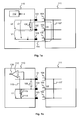
Figure 1 a shows an arrangement according to an embodiment of the invention for detecting a situation in which a firstelectrical device 110 is connected to a secondelectrical device 111. Theelectrical device 110 comprises a firstelectrical contact terminal 101, a secondelectrical contact terminal 102, and a thirdelectrical contact terminal 103. The said electrical contact terminals can be, for example, electrical contact terminals, e.g. pins or contact strips, of an electrical connector. Non-zero voltage V1 is arranged to prevail between theelectrical contact terminals electrical device 111 comprises afirst counterpart 104 that is arranged to fit with theelectrical contact terminal 101, asecond counterpart 105 that is arranged to fit with theelectrical contact terminal 102, and athird counterpart 106 that is arranged to fit with theelectrical contact terminal 103. Theelectrical device 111 comprises agalvanic contact 107 between thecounterpart 104 and thecounterpart 106. The arrangement for detecting a situation in which theelectrical device 110 is connected to theelectrical device 111 comprises aresistor 108 that is connected between theelectrical contact terminal 101 and theelectrical contact terminal 102. The arrangement comprises adetector 112 that is arranged to detect the situation in which theelectrical device 110 is connected to theelectrical device 111 on the basis of a change of an electrical quantity e associated with theresistor 108. When theelectrical device 110 is connected to theelectrical device 111, i.e. theelectrical contact terminals counterparts path 140 for electrical current is formed and a change in an electrical quantity associated with theresistor 108 takes place. - In an arrangement according to an embodiment of the invention the
detector 112 is arranged to detect the situation in which theelectrical device 110 is connected to theelectrical device 111 on the basis of a change of electrical current i flowing via theelectrical contact terminal 103. In this embodiment, the electrical current i represents the electrical quantity e associated with theresistor 108. - In an arrangement according to an embodiment of the invention the
detector 112 is arranged to detect the situation in which theelectrical device 110 is connected to theelectrical device 111 on the basis of a change of voltage v2 between theelectrical contact terminals resistor 108. - In an arrangement according to an embodiment of the invention the
detector 112 is arranged to detect the situation in which theelectrical device 110 is connected to theelectrical device 111 on the basis of a change of voltage v3 between theelectrical contact terminals resistor 108. - In an arrangement according to an embodiment of the invention the
detector 112 is arranged to detect the situation in which theelectrical device 110 is connected to theelectrical device 111 on the basis of a change of electrical power P = V1 × i supplied by theelectrical device 110 to theelectrical contact terminals resistor 108. -
Figure 1 a shows an arrangement according to an embodiment of the invention in which acomparator 112 constitutes the detector that is arranged to detect the situation in which theelectrical device 110 is connected to theelectrical device 111. When theelectrical device 110 is not connected to theelectrical device 111, electrical potential of theelectrical contact terminal 101 is the same as electrical potential of theelectrical contact terminal 102, i.e. there is no electrical current, and thus no voltage loss, in theresistor 108. Electrical potential of anode 115 is lower than the electrical potential of theelectrical contact terminal 102 but higher than electrical potential of theelectrical contact terminal 103. Therefore, anoutput terminal 109 of thecomparator 112 is at a low voltage. The electrical potential of thenode 115 depends on values ofvoltage division resistors electrical device 110 is connected to theelectrical device 111, the electrical potential of theelectrical contact terminal 101 is substantially the same as the electrical potential of theelectrical contact terminal 103, i.e. thecurrent path 140 is formed. Therefore, anoutput terminal 109 of thecomparator 112 is at a high voltage. Thus, thecomparator 112 is arranged to detect whether or not theelectrical device 110 is connected to theelectrical device 111. -
Figure 2 shows an arrangement according to an embodiment of the invention for detecting a situation in which a firstelectrical device 210 is connected to a secondelectrical device 211. Theelectrical device 210 comprises a firstelectrical contact terminal 201, a secondelectrical contact terminal 202, and a thirdelectrical contact terminal 203. Theelectrical contact terminal 201 is a metal shield of an USB-connector 250 (Universal Serial Bus), theelectrical contact terminal 202 is a contact strip of the USB-connector, and theelectrical contact terminal 203 is another contact strip of the USB-connector. Non-zero voltage V1 is arranged to prevail between the contact strips 202 and 203. Theelectrical device 211 comprises acounterpart 251 for the USB-connector. Thecounterpart 251 for the USB-connector comprises ametal shield 204 that is arranged to fit with themetal shield 201, acontact strip 205 that is arranged to fit with thecontact strip 202, and acontact strip 206 that is arranged to fit with thecontact strip 203. There is agalvanic contact 207 between themetal shield 204 and thecontact strip 206. - The arrangement for detecting a situation in which the
electrical device 210 is connected to theelectrical device 211 comprises aresistor 208 that is connected between themetal shield 201 and thecontact strip 202. The arrangement comprises adetector 212 that is arranged to detect the situation in which theelectrical device 210 is connected to theelectrical device 211 on the basis of a change of electrical power P supplied bycircuitry 220 to the contact strips 202 and 203. -
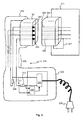
Figure 3 shows anelectrical device 310 according to an embodiment of the invention. The electrical device comprises a firstelectrical contact terminal 301, a secondelectrical contact terminal 302, and a thirdelectrical contact terminal 303. Non-zero voltage V1 is arranged to prevail between theelectrical contact terminal 302 and theelectrical contact terminal 303. The electrical device comprises aresistor 308 that is connected between theelectrical contact terminal 301 and theelectrical contact terminal 302. The electrical device comprises adetector 312 that is arranged to detect a situation in which theelectrical device 310 is connected to anotherelectrical device 311 on the basis of a change of an electrical quantity associated with theresistor 108. Thedetector 312 is arranged to detect the situation in which the electrical device is connected to the other electrical device on the basis of a change of electrical current flowing via theelectrical contact terminal 303. The electrical current is indicated with the aid of ashunt resistor 313 and voltage across the shunt resistor is given as an input quantity to thedetector 312. Theelectrical device 310 comprises aconnector 324 that is coupled with acable 323 toother parts 325 of the electrical device. - In an electrical device according to a first alternative embodiment of the invention the
detector 312 is arranged to detect the situation in which theelectrical device 310 is connected to the otherelectrical device 311 on the basis of a change of voltage between theelectrical contact terminal 301 and theelectrical contact terminal 303. - In an electrical device according to a second alternative embodiment of the invention the
detector 312 is arranged to detect the situation in which theelectrical device 310 is connected to the otherelectrical device 311 on the basis of a change of electrical power supplied by the electrical device to theelectrical contact terminals - An electrical device according to an embodiment of the invention comprises a
control circuitry 322 that is arranged to perform a pre-determined control action as a response to a situation in which the change of the electrical quantity associated with the resistor is detected. Thecontrol circuitry 322 can be, for example, a programmable processor or a dedicated integrated circuit. It is also possible that thedetector 312 is a part of thecontrol circuitry 322. - In an electrical device according to an embodiment of the invention the
control circuitry 322 is arranged to reduce power consumption of theelectrical device 310 as a response to a situation in which the change of the electrical quantity associated with the resistor is indicative of a decrease of power dissipated in theresistor 308, i.e. the change of the electrical quantity indicates a situation in which the electrical device is disconnected from the other electrical device. - In an electrical device according to an embodiment of the invention the
control circuitry 322 is arranged to activate a pre-determined operation of theelectrical device 310 as a response to a situation in which the change of the electrical quantity associated with the resistor is indicative of an increase of power dissipated in theresistor 308, i.e. the change of the electrical quantity indicates a situation in which the electrical device is connected to the other electrical device. - An electrical device according to an embodiment of the invention is a charger device capable of supplying electrical power to the other
electrical device 311. The otherelectrical device 311 can be, for example, a mobile phone or a palmtop computer. - In an electrical device according to an embodiment of the invention the
electrical contact terminal 301 is a metal shield of an USB-connector (Universal Serial Bus), theelectrical contact terminal 302 is a contact strip of the USB-connector, and theelectrical contact terminal 303 is another contact strip of the USB-connector. - In an electrical device according to an embodiment of the invention the
control circuitry 322 is arranged to reduce the voltage between theelectrical contact terminal 302 and theelectrical contact terminal 303 to a first pre-determined non-zero value as response to a situation in which the change of the electrical quantity associated with theresistor 308 is indicative of a decrease of a power dissipated in the resistor, i.e. the change of the electrical quantity indicates a situation in which the electrical device is disconnected from the otherelectrical device 311. The above-described functionality is advantageous, for example, in a charger device because undesirable energy loss can be reduced in a situation in which the charger device is energized but not connected to the otherelectrical device 311. - In an electrical device according to an embodiment of the invention the
control circuitry 322 is arranged to increase the voltage between theelectrical contact terminal 302 and theelectrical contact terminal 302 to a second pre-determined non-zero value as response to a situation in which the change of the electrical quantity associated with theresistor 308 is indicative of an increase of a power dissipated in the resistor, i.e. the change of the electrical quantity indicates a situation in which the electrical device is connected to the otherelectrical device 311. -
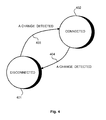
Figure 4 shows a state diagram of a method according to an embodiment of the invention for detecting a situation in which a first electrical device is connected to a second electrical device. The first electrical device 110 (numbers greater than 100 and less than 200 refer tofigure 1 a) comprises: - a first
electrical contact terminal 101, - a second
electrical contact terminal 102, and - a third
electrical contact terminal 103, non-zero voltage V1 being arranged to prevail between the second electrical contact terminal and the third electrical contact terminal. - The second
electrical device 111 comprises: - a
first counterpart 104 for the first electrical contact terminal, - a
second counterpart 105 for the second electrical contact terminal, and - a
third counterpart 106 for the third electrical contact terminal, the first counterpart having agalvanic contact 107 with the third counterpart, - The situation in which the first electrical device is connected to the second electrical device is detected on the basis of a change of an electrical quantity associated with a
resistor 108 connected between the first electrical contact terminal and the second electrical contact terminal. When the first electrical device is connected to the second electrical device, i.e. a transition from astate 401 to astate 402 takes place, the following path for electrical current is formed: the second electrical contact terminal 102 - the resistor 108 - the first electrical contact terminal 101 - the first counterpart 104 - thegalvanic contact 107 between the first and third counterpart - the third counterpart 106 - the thirdelectrical contact terminal 103. As a consequence, a change in an electrical quantity associated with theresistor 108 can be detected 403. When the first electrical device is disconnected from the second electrical device, i.e. a transition from thestate 402 to thestate 401 takes place, the above-described path for the electrical current is broken. As a consequence, a change in an electrical quantity associated with theresistor 108 can be detected 404. - In a method according to an embodiment of the invention the first electrical contact terminal is a metal shield of an USB-connector (Universal Serial Bus), the second electrical contact terminal is a contact strip of the USB-connector, and the third electrical contact terminal is another contact strip of the USB-connector.
- In a method according to an embodiment of the invention the situation in which the first electrical device is connected to the second electrical device is detected on the basis of a change of electrical current flowing via the third electrical contact terminal.
- In a method according to an embodiment of the invention the situation in which the first electrical device is connected to the second electrical device is detected on the basis of a change of voltage between the first electrical contact terminal and the third electrical contact terminal.
- In a method according to an embodiment of the invention the situation in which the first electrical device is connected to the second electrical device is detected on the basis of a change of electrical power supplied by the first electrical device to the first electrical contact terminal and the second electrical contact terminal
- While there have been shown and described and pointed out fundamental novel features of the invention as applied to embodiments thereof, it will be understood that various omissions and substitutions and changes in the form and details of the devices and methods described may be made by those skilled in the art without departing from the spirit of the invention. For example, it is expressly intended that all combinations of those elements and/or method steps which perform substantially the same function in substantially the same way to achieve the same results are within the scope of the invention. Moreover, it should be recognized that structures and/or elements and/or method steps shown and/or described in connection with any disclosed form or embodiment of the invention may be incorporated in any other disclosed or described or suggested form or embodiment as a general matter of design choice. The specific examples provided in the description given above should not be construed as limiting. Therefore, the invention is not limited merely to the embodiments described above, many variants being possible without departing from the scope of the inventive idea.
Claims (15)
- An electrical device, comprising:- a first electrical contact terminal (101, 201, 301),- a second electrical contact terminal (102, 202, 302),- a third electrical contact terminal (103, 203, 303), non-zero voltage being arranged to prevail between the second electrical contact terminal and the third electrical contact terminal,- a resistor (108, 208, 308) connected between the first electrical contact terminal and the second electrical contact terminal, and- a detector (112, 212, 312) arranged to detect a situation in which the electrical device is connected to another electrical device on the basis of a change of an electrical quantity associated with the resistor,characterised in that the electrical device comprises a control circuitry (322) arranged to reduce power consumption of the electrical device as a response to a situation in which the change of the electrical quantity associated with the resistor is indicative of a decrease of power dissipated in the resistor.
- An electrical device according to claim 1, characterised in that the detector (312) is arranged to detect the situation in which the electrical device is connected to the other electrical device on the basis of a change of electrical current flowing via the third electrical contact terminal.
- An electrical device according to claim 1, characterised in that the detector (112) is arranged to detect the situation in which the electrical device is connected to the other electrical device on the basis of a change of voltage between the first electrical contact terminal and the third electrical contact terminal.
- An electrical device according to claim 1, characterised in that the detector (212) is arranged to detect the situation in which the electrical device is connected to the other electrical device on the basis of a change of electrical power supplied by the electrical device to the first electrical contact terminal and the second electrical contact terminal.
- An electrical device according to claim 1, characterised in that the control circuitry is arranged to activate a pre-determined operation of the electrical device as a response to a situation in which the change of the electrical quantity associated with the resistor is indicative of an increase of power dissipated in the resistor.
- An electrical device according to claim 1, characterised in that the electrical device is a charger device capable of supplying electrical power to the other electrical device (311).
- An electrical device according to claim 1 or 6, characterised in that the first electrical contact terminal is a metal shield (201, 301) of an USB-connector (Universal Serial Bus), the second electrical contact terminal is a contact strip (202, 302) of the USB-connector, and the third electrical contact terminal is another contact strip (203, 303) of the USB-connector.
- An electrical device according to claim 6, characterised in that the control circuitry (322) is arranged to reduce the voltage between the second electrical contact terminal and the third electrical contact terminal to a first pre-determined non-zero value as response to a situation in which the change of the electrical quantity associated with the resistor is indicative of a decrease of a power dissipated in the resistor.
- An electrical device according to claim 6 or 8, characterised in that the control circuitry (322) arranged to increase the voltage between the second electrical contact terminal and the third electrical contact terminal to a second pre-determined non-zero value as response to a situation in which the change of the electrical quantity associated with the resistor is indicative of an increase of a power dissipated in the resistor.
- An arrangement for detecting a situation in which a first electrical device (110, 210, 310) is connected to a second electrical device (111, 211, 311), the first electrical device comprising:- a first electrical contact terminal (101, 201, 301),- a second electrical contact terminal (102, 202, 302), and- a third electrical contact terminal (103, 203, 303), non-zero voltage being arranged to prevail between the second electrical contact terminal and the third electrical contact terminal, andthe second electrical device comprising:- a first counterpart (104, 204, 304) for the first electrical contact terminal,- a second counterpart (105, 205, 305) for the second electrical contact terminal, and- a third counterpart (106, 206, 306) for the third electrical contact terminal, the first counterpart having a galvanic contact with the third counterpart, andwherein the arrangement comprises:- a resistor (108, 208, 308) connected between the first electrical contact terminal and the second electrical contact terminal, and- a detector (112, 212, 312) arranged to detect the situation in which the first electrical device is connected to the second electrical device on the basis of a change of an electrical quantity associated with the resistor,characterised in that the arrangement comprises a control circuitry (322) arranged to reduce power consumption of the first electrical device as a response to a situation in which the change of the electrical quantity associated with the resistor is indicative of a decrease of power dissipated in the resistor.
- An arrangement according to claim 10, characterised in that the first electrical contact terminal is a metal shield (201, 301) of an USB-connector (Universal Serial Bus), the second electrical contact terminal is a contact strip (202, 302) of the USB-connector, and the third electrical contact terminal is another contact strip (203, 303) of the USB-connector.
- An arrangement according to claim 10, characterised in that the detector (312) is arranged to detect the situation in which the first electrical device is connected to the second electrical device on the basis of a change of electrical current flowing via the third electrical contact terminal.
- An arrangement according to claim 10, characterised in that the detector (112) is arranged to detect the situation in which the first electrical device is connected to the second electrical device on the basis of a change of voltage between the first electrical contact terminal and the third electrical contact terminal.
- An arrangement according to claim 10, characterised in that the detector (212) is arranged to detect the situation in which the first electrical device is connected to the second electrical device on the basis of a change of electrical power supplied by the first electrical device to the first electrical contact terminal and the second electrical contact terminal.
- A method for detecting a situation in which a first electrical device is connected to a second electrical device, the first electrical device comprising:- a first electrical contact terminal,- a second electrical contact terminal, and- a third electrical contact terminal, non-zero voltage being arranged to prevail between the second electrical contact terminal and the third electrical contact terminal, andthe second electrical device comprising:- a first counterpart for the first electrical contact terminal,- a second counterpart for the second electrical contact terminal, and- a third counterpart for the third electrical contact terminal, the first counterpart having a galvanic contact with the third counterpart,wherein the method comprises detecting (430) the situation in which the first electrical device is connected to the second electrical device on the basis of a change of an electrical quantity associated with a resistor connected between the first electrical contact terminal and the second electrical contact terminal, characterised in that the method further comprises reducing power consumption of the first electrical device as a response to a situation in which the change of the electrical quantity associated with the resistor is indicative of a decrease of power dissipated in the resistor.
Applications Claiming Priority (1)
| Application Number | Priority Date | Filing Date | Title |
|---|---|---|---|
| FI20070909A FI121401B (en) | 2007-11-27 | 2007-11-27 | Method and arrangement for checking an electrical device |
Publications (3)
| Publication Number | Publication Date |
|---|---|
| EP2071428A2 true EP2071428A2 (en) | 2009-06-17 |
| EP2071428A3 EP2071428A3 (en) | 2017-04-12 |
| EP2071428B1 EP2071428B1 (en) | 2018-06-13 |
Family
ID=38786687
Family Applications (1)
| Application Number | Title | Priority Date | Filing Date |
|---|---|---|---|
| EP08169995.1A Not-in-force EP2071428B1 (en) | 2007-11-27 | 2008-11-26 | Method and arrangement for controlling an electrical device |
Country Status (3)
| Country | Link |
|---|---|
| US (1) | US8242752B2 (en) |
| EP (1) | EP2071428B1 (en) |
| FI (1) | FI121401B (en) |
Cited By (3)
| Publication number | Priority date | Publication date | Assignee | Title |
|---|---|---|---|---|
| FR2995100A1 (en) * | 2012-09-05 | 2014-03-07 | Peugeot Citroen Automobiles Sa | ELECTRONIC EQUIPMENT CAPABLE OF GENERATING A POWER SUPPLY VOLTAGE TO FEED A NOMADIC APPARATUS |
| EP2383861A3 (en) * | 2010-04-06 | 2014-10-08 | Semiconductor Components Industries, LLC | Battery charger for portable electronic equipment |
| CN107706977A (en) * | 2017-10-16 | 2018-02-16 | 广东欧珀移动通信有限公司 | Method for detecting charging current and charging device |
Families Citing this family (11)
| Publication number | Priority date | Publication date | Assignee | Title |
|---|---|---|---|---|
| US8717044B2 (en) * | 2010-04-23 | 2014-05-06 | Apple Inc. | Charging systems with direct charging port support and extended capabilities |
| US8386108B2 (en) * | 2011-03-02 | 2013-02-26 | Bombardier Transportation Gmbh | System and method of controlling supply voltage polarity on a vehicle |
| JP2012191744A (en) * | 2011-03-10 | 2012-10-04 | Semiconductor Components Industries Llc | Battery charger for portable electronic apparatus |
| US9020648B2 (en) | 2011-04-19 | 2015-04-28 | Cooper Technologies Company | Zero power appliance control, systems and methods |
| US9805890B2 (en) | 2011-11-07 | 2017-10-31 | Cooper Technologies Company | Electronic device state detection for zero power charger control, systems and methods |
| US9563244B2 (en) | 2013-01-08 | 2017-02-07 | Hzo, Inc. | Apparatuses, systems, and methods for reducing power to ports of electronic devices |
| CN103138354A (en) * | 2013-03-26 | 2013-06-05 | 无锡市崇安区科技创业服务中心 | Charger |
| GB201413032D0 (en) | 2014-02-28 | 2014-09-03 | Beyond Twenty Ltd | Beyond 7 |
| FR3090888B1 (en) * | 2018-12-19 | 2020-11-27 | Continental Automotive France | Device for automatic detection of coupling between electronic devices |
| FR3112869B1 (en) * | 2020-07-21 | 2022-06-24 | Vitesco Technologies | Device for automatic detection of coupling between electronic devices |
| FR3112871B1 (en) * | 2020-07-21 | 2022-08-26 | Vitesco Technologies | Device for automatic detection of coupling between electronic devices |
Family Cites Families (9)
| Publication number | Priority date | Publication date | Assignee | Title |
|---|---|---|---|---|
| JPH06309071A (en) | 1993-04-19 | 1994-11-04 | Matsushita Electric Ind Co Ltd | Power saving circuit |
| US6339314B1 (en) * | 2000-12-27 | 2002-01-15 | Philips Electronics North America Corporation | Battery charger circuit with low standby power dissipation |
| JP2002318647A (en) * | 2001-04-19 | 2002-10-31 | Mitsubishi Electric Corp | Detecting device and detecting method thereof |
| DE10202603B4 (en) * | 2002-01-24 | 2012-08-30 | Robert Bosch Gmbh | Method and device for slowing down the discharge process of a battery |
| US7268561B2 (en) * | 2004-09-20 | 2007-09-11 | Texas Instruments Incorporated | USB attach detection for USB 1.1 and USB OTG devices |
| US20070018611A1 (en) * | 2005-07-11 | 2007-01-25 | Nokia Corporation | Battery detection interface |
| TWI296370B (en) * | 2005-10-18 | 2008-05-01 | Rdc Semiconductor Co Ltd | Peripheral device connection current compensation circuit |
| CN1976163A (en) * | 2006-12-06 | 2007-06-06 | 华为技术有限公司 | Charger type distinguishing system, terminal charging method, terminal and charger |
| US7644217B2 (en) * | 2007-03-02 | 2010-01-05 | Microchip Technology Incorporated | Detecting connection to a USB host or hub without using an extra status input |
-
2007
- 2007-11-27 FI FI20070909A patent/FI121401B/en active IP Right Grant
-
2008
- 2008-11-20 US US12/313,666 patent/US8242752B2/en not_active Expired - Fee Related
- 2008-11-26 EP EP08169995.1A patent/EP2071428B1/en not_active Not-in-force
Cited By (4)
| Publication number | Priority date | Publication date | Assignee | Title |
|---|---|---|---|---|
| EP2383861A3 (en) * | 2010-04-06 | 2014-10-08 | Semiconductor Components Industries, LLC | Battery charger for portable electronic equipment |
| FR2995100A1 (en) * | 2012-09-05 | 2014-03-07 | Peugeot Citroen Automobiles Sa | ELECTRONIC EQUIPMENT CAPABLE OF GENERATING A POWER SUPPLY VOLTAGE TO FEED A NOMADIC APPARATUS |
| WO2014037642A1 (en) * | 2012-09-05 | 2014-03-13 | Peugeot Citroen Automobiles Sa | Electronic device suitable for generating power supply voltage intended for supplying power to a mobile apparatus |
| CN107706977A (en) * | 2017-10-16 | 2018-02-16 | 广东欧珀移动通信有限公司 | Method for detecting charging current and charging device |
Also Published As
| Publication number | Publication date |
|---|---|
| US8242752B2 (en) | 2012-08-14 |
| FI20070909L (en) | 2009-05-28 |
| FI20070909A0 (en) | 2007-11-27 |
| FI121401B (en) | 2010-10-29 |
| EP2071428B1 (en) | 2018-06-13 |
| US20090128099A1 (en) | 2009-05-21 |
| EP2071428A3 (en) | 2017-04-12 |
Similar Documents
| Publication | Publication Date | Title |
|---|---|---|
| EP2071428A2 (en) | Method and arrangement for controlling an electrical device | |
| CN101651359B (en) | Power supply unit and power supply switching method of mobile terminal | |
| US7932636B2 (en) | Automatic start-up circuit and uninterruptible power supply apparatus having such automatic start-up circuit | |
| DK3101756T3 (en) | CHARGING SYSTEM | |
| EP2550718B1 (en) | A system and method for providing a high efficiency bypass circuit for multi-stage dc-dc converters used in battery powered systems | |
| EP2383861A2 (en) | Battery charger for portable electronic equipment | |
| US20080247203A1 (en) | Energy Efficient Power Converter | |
| US20140354047A1 (en) | Battery Assisted Power | |
| JP2013110823A (en) | Electronic apparatus, charge control method, charging system, and data transfer system | |
| CN101546918A (en) | Device and method for charging USB | |
| CN108628431A (en) | Electronic equipment and its certainly energy consumption control circuit | |
| EP2760106A1 (en) | Rechargeable electrical device | |
| JP2018121516A (en) | Controlling power delivery to battery | |
| KR100584324B1 (en) | Power control device of composite terminal | |
| EP4265468A1 (en) | Method and equipment for charging an electric vehicle | |
| JP2018063558A (en) | Power supply control circuit, electronic device, and power supply control method | |
| CN101893925B (en) | Start circuit | |
| CN115237235B (en) | USB equipment shift-out identification circuit and method and power supply system | |
| CN208421767U (en) | Electronic equipment and its self-consumption control circuit | |
| CN112636418A (en) | Charging system, charging method, mobile terminal and charger | |
| WO2017134346A1 (en) | Method for maintaining a battery | |
| CN112858894A (en) | Detection method and detection device for working state of contactor, storage medium and vehicle | |
| CN104638898A (en) | Soft start control device system | |
| CN115549258A (en) | Charging circuit, charging method and electronic device | |
| JP2005261142A (en) | Charging circuit |
Legal Events
| Date | Code | Title | Description |
|---|---|---|---|
| PUAI | Public reference made under article 153(3) epc to a published international application that has entered the european phase |
Free format text: ORIGINAL CODE: 0009012 |
|
| AK | Designated contracting states |
Kind code of ref document: A2 Designated state(s): AT BE BG CH CY CZ DE DK EE ES FI FR GB GR HR HU IE IS IT LI LT LU LV MC MT NL NO PL PT RO SE SI SK TR |
|
| AX | Request for extension of the european patent |
Extension state: AL BA MK RS |
|
| PUAL | Search report despatched |
Free format text: ORIGINAL CODE: 0009013 |
|
| AK | Designated contracting states |
Kind code of ref document: A3 Designated state(s): AT BE BG CH CY CZ DE DK EE ES FI FR GB GR HR HU IE IS IT LI LT LU LV MC MT NL NO PL PT RO SE SI SK TR |
|
| AX | Request for extension of the european patent |
Extension state: AL BA MK RS |
|
| RIC1 | Information provided on ipc code assigned before grant |
Ipc: H02J 7/00 20060101ALI20170308BHEP Ipc: H02J 9/00 20060101ALI20170308BHEP Ipc: H02J 7/02 20160101ALN20170308BHEP Ipc: G06F 1/26 20060101AFI20170308BHEP |
|
| 17P | Request for examination filed |
Effective date: 20170912 |
|
| RBV | Designated contracting states (corrected) |
Designated state(s): AT BE BG CH CY CZ DE DK EE ES FI FR GB GR HR HU IE IS IT LI LT LU LV MC MT NL NO PL PT RO SE SI SK TR |
|
| AKX | Designation fees paid |
Designated state(s): AT BE BG CH CY CZ DE DK EE ES FI FR GB GR HR HU IE IS IT LI LT LU LV MC MT NL NO PL PT RO SE SI SK TR |
|
| AXX | Extension fees paid |
Extension state: AL Extension state: MK Extension state: BA Extension state: RS |
|
| GRAP | Despatch of communication of intention to grant a patent |
Free format text: ORIGINAL CODE: EPIDOSNIGR1 |
|
| RIC1 | Information provided on ipc code assigned before grant |
Ipc: H02J 9/00 20060101ALI20171221BHEP Ipc: H02J 7/00 20060101ALI20171221BHEP Ipc: G06F 1/26 20060101AFI20171221BHEP Ipc: H02J 7/02 20160101ALN20171221BHEP |
|
| INTG | Intention to grant announced |
Effective date: 20180109 |
|
| GRAS | Grant fee paid |
Free format text: ORIGINAL CODE: EPIDOSNIGR3 |
|
| GRAA | (expected) grant |
Free format text: ORIGINAL CODE: 0009210 |
|
| AK | Designated contracting states |
Kind code of ref document: B1 Designated state(s): AT BE BG CH CY CZ DE DK EE ES FI FR GB GR HR HU IE IS IT LI LT LU LV MC MT NL NO PL PT RO SE SI SK TR |
|
| REG | Reference to a national code |
Ref country code: GB Ref legal event code: FG4D |
|
| REG | Reference to a national code |
Ref country code: CH Ref legal event code: EP Ref country code: AT Ref legal event code: REF Ref document number: 1009119 Country of ref document: AT Kind code of ref document: T Effective date: 20180615 |
|
| REG | Reference to a national code |
Ref country code: IE Ref legal event code: FG4D |
|
| REG | Reference to a national code |
Ref country code: DE Ref legal event code: R096 Ref document number: 602008055587 Country of ref document: DE |
|
| REG | Reference to a national code |
Ref country code: NL Ref legal event code: MP Effective date: 20180613 |
|
| REG | Reference to a national code |
Ref country code: LT Ref legal event code: MG4D |
|
| PG25 | Lapsed in a contracting state [announced via postgrant information from national office to epo] |
Ref country code: NO Free format text: LAPSE BECAUSE OF FAILURE TO SUBMIT A TRANSLATION OF THE DESCRIPTION OR TO PAY THE FEE WITHIN THE PRESCRIBED TIME-LIMIT Effective date: 20180913 Ref country code: FI Free format text: LAPSE BECAUSE OF FAILURE TO SUBMIT A TRANSLATION OF THE DESCRIPTION OR TO PAY THE FEE WITHIN THE PRESCRIBED TIME-LIMIT Effective date: 20180613 Ref country code: LT Free format text: LAPSE BECAUSE OF FAILURE TO SUBMIT A TRANSLATION OF THE DESCRIPTION OR TO PAY THE FEE WITHIN THE PRESCRIBED TIME-LIMIT Effective date: 20180613 Ref country code: BG Free format text: LAPSE BECAUSE OF FAILURE TO SUBMIT A TRANSLATION OF THE DESCRIPTION OR TO PAY THE FEE WITHIN THE PRESCRIBED TIME-LIMIT Effective date: 20180913 Ref country code: CY Free format text: LAPSE BECAUSE OF FAILURE TO SUBMIT A TRANSLATION OF THE DESCRIPTION OR TO PAY THE FEE WITHIN THE PRESCRIBED TIME-LIMIT Effective date: 20180613 Ref country code: ES Free format text: LAPSE BECAUSE OF FAILURE TO SUBMIT A TRANSLATION OF THE DESCRIPTION OR TO PAY THE FEE WITHIN THE PRESCRIBED TIME-LIMIT Effective date: 20180613 Ref country code: SE Free format text: LAPSE BECAUSE OF FAILURE TO SUBMIT A TRANSLATION OF THE DESCRIPTION OR TO PAY THE FEE WITHIN THE PRESCRIBED TIME-LIMIT Effective date: 20180613 |
|
| PG25 | Lapsed in a contracting state [announced via postgrant information from national office to epo] |
Ref country code: HR Free format text: LAPSE BECAUSE OF FAILURE TO SUBMIT A TRANSLATION OF THE DESCRIPTION OR TO PAY THE FEE WITHIN THE PRESCRIBED TIME-LIMIT Effective date: 20180613 Ref country code: LV Free format text: LAPSE BECAUSE OF FAILURE TO SUBMIT A TRANSLATION OF THE DESCRIPTION OR TO PAY THE FEE WITHIN THE PRESCRIBED TIME-LIMIT Effective date: 20180613 Ref country code: GR Free format text: LAPSE BECAUSE OF FAILURE TO SUBMIT A TRANSLATION OF THE DESCRIPTION OR TO PAY THE FEE WITHIN THE PRESCRIBED TIME-LIMIT Effective date: 20180914 |
|
| REG | Reference to a national code |
Ref country code: AT Ref legal event code: MK05 Ref document number: 1009119 Country of ref document: AT Kind code of ref document: T Effective date: 20180613 |
|
| PG25 | Lapsed in a contracting state [announced via postgrant information from national office to epo] |
Ref country code: NL Free format text: LAPSE BECAUSE OF FAILURE TO SUBMIT A TRANSLATION OF THE DESCRIPTION OR TO PAY THE FEE WITHIN THE PRESCRIBED TIME-LIMIT Effective date: 20180613 |
|
| PG25 | Lapsed in a contracting state [announced via postgrant information from national office to epo] |
Ref country code: SK Free format text: LAPSE BECAUSE OF FAILURE TO SUBMIT A TRANSLATION OF THE DESCRIPTION OR TO PAY THE FEE WITHIN THE PRESCRIBED TIME-LIMIT Effective date: 20180613 Ref country code: PL Free format text: LAPSE BECAUSE OF FAILURE TO SUBMIT A TRANSLATION OF THE DESCRIPTION OR TO PAY THE FEE WITHIN THE PRESCRIBED TIME-LIMIT Effective date: 20180613 Ref country code: RO Free format text: LAPSE BECAUSE OF FAILURE TO SUBMIT A TRANSLATION OF THE DESCRIPTION OR TO PAY THE FEE WITHIN THE PRESCRIBED TIME-LIMIT Effective date: 20180613 Ref country code: CZ Free format text: LAPSE BECAUSE OF FAILURE TO SUBMIT A TRANSLATION OF THE DESCRIPTION OR TO PAY THE FEE WITHIN THE PRESCRIBED TIME-LIMIT Effective date: 20180613 Ref country code: AT Free format text: LAPSE BECAUSE OF FAILURE TO SUBMIT A TRANSLATION OF THE DESCRIPTION OR TO PAY THE FEE WITHIN THE PRESCRIBED TIME-LIMIT Effective date: 20180613 Ref country code: EE Free format text: LAPSE BECAUSE OF FAILURE TO SUBMIT A TRANSLATION OF THE DESCRIPTION OR TO PAY THE FEE WITHIN THE PRESCRIBED TIME-LIMIT Effective date: 20180613 Ref country code: IS Free format text: LAPSE BECAUSE OF FAILURE TO SUBMIT A TRANSLATION OF THE DESCRIPTION OR TO PAY THE FEE WITHIN THE PRESCRIBED TIME-LIMIT Effective date: 20181013 |
|
| PG25 | Lapsed in a contracting state [announced via postgrant information from national office to epo] |
Ref country code: IT Free format text: LAPSE BECAUSE OF FAILURE TO SUBMIT A TRANSLATION OF THE DESCRIPTION OR TO PAY THE FEE WITHIN THE PRESCRIBED TIME-LIMIT Effective date: 20180613 |
|
| REG | Reference to a national code |
Ref country code: DE Ref legal event code: R097 Ref document number: 602008055587 Country of ref document: DE |
|
| PLBE | No opposition filed within time limit |
Free format text: ORIGINAL CODE: 0009261 |
|
| STAA | Information on the status of an ep patent application or granted ep patent |
Free format text: STATUS: NO OPPOSITION FILED WITHIN TIME LIMIT |
|
| 26N | No opposition filed |
Effective date: 20190314 |
|
| PG25 | Lapsed in a contracting state [announced via postgrant information from national office to epo] |
Ref country code: SI Free format text: LAPSE BECAUSE OF FAILURE TO SUBMIT A TRANSLATION OF THE DESCRIPTION OR TO PAY THE FEE WITHIN THE PRESCRIBED TIME-LIMIT Effective date: 20180613 Ref country code: DK Free format text: LAPSE BECAUSE OF FAILURE TO SUBMIT A TRANSLATION OF THE DESCRIPTION OR TO PAY THE FEE WITHIN THE PRESCRIBED TIME-LIMIT Effective date: 20180613 |
|
| REG | Reference to a national code |
Ref country code: CH Ref legal event code: PL |
|
| PG25 | Lapsed in a contracting state [announced via postgrant information from national office to epo] |
Ref country code: MC Free format text: LAPSE BECAUSE OF FAILURE TO SUBMIT A TRANSLATION OF THE DESCRIPTION OR TO PAY THE FEE WITHIN THE PRESCRIBED TIME-LIMIT Effective date: 20180613 Ref country code: LU Free format text: LAPSE BECAUSE OF NON-PAYMENT OF DUE FEES Effective date: 20181126 |
|
| REG | Reference to a national code |
Ref country code: BE Ref legal event code: MM Effective date: 20181130 |
|
| REG | Reference to a national code |
Ref country code: IE Ref legal event code: MM4A |
|
| PG25 | Lapsed in a contracting state [announced via postgrant information from national office to epo] |
Ref country code: CH Free format text: LAPSE BECAUSE OF NON-PAYMENT OF DUE FEES Effective date: 20181130 Ref country code: LI Free format text: LAPSE BECAUSE OF NON-PAYMENT OF DUE FEES Effective date: 20181130 |
|
| PG25 | Lapsed in a contracting state [announced via postgrant information from national office to epo] |
Ref country code: IE Free format text: LAPSE BECAUSE OF NON-PAYMENT OF DUE FEES Effective date: 20181126 |
|
| PG25 | Lapsed in a contracting state [announced via postgrant information from national office to epo] |
Ref country code: BE Free format text: LAPSE BECAUSE OF NON-PAYMENT OF DUE FEES Effective date: 20181130 |
|
| PG25 | Lapsed in a contracting state [announced via postgrant information from national office to epo] |
Ref country code: MT Free format text: LAPSE BECAUSE OF NON-PAYMENT OF DUE FEES Effective date: 20181126 |
|
| PG25 | Lapsed in a contracting state [announced via postgrant information from national office to epo] |
Ref country code: TR Free format text: LAPSE BECAUSE OF FAILURE TO SUBMIT A TRANSLATION OF THE DESCRIPTION OR TO PAY THE FEE WITHIN THE PRESCRIBED TIME-LIMIT Effective date: 20180613 |
|
| PG25 | Lapsed in a contracting state [announced via postgrant information from national office to epo] |
Ref country code: PT Free format text: LAPSE BECAUSE OF FAILURE TO SUBMIT A TRANSLATION OF THE DESCRIPTION OR TO PAY THE FEE WITHIN THE PRESCRIBED TIME-LIMIT Effective date: 20180613 |
|
| PG25 | Lapsed in a contracting state [announced via postgrant information from national office to epo] |
Ref country code: HU Free format text: LAPSE BECAUSE OF FAILURE TO SUBMIT A TRANSLATION OF THE DESCRIPTION OR TO PAY THE FEE WITHIN THE PRESCRIBED TIME-LIMIT; INVALID AB INITIO Effective date: 20081126 |
|
| PGFP | Annual fee paid to national office [announced via postgrant information from national office to epo] |
Ref country code: GB Payment date: 20211118 Year of fee payment: 14 Ref country code: FR Payment date: 20211115 Year of fee payment: 14 Ref country code: DE Payment date: 20211119 Year of fee payment: 14 |
|
| REG | Reference to a national code |
Ref country code: DE Ref legal event code: R119 Ref document number: 602008055587 Country of ref document: DE |
|
| GBPC | Gb: european patent ceased through non-payment of renewal fee |
Effective date: 20221126 |
|
| PG25 | Lapsed in a contracting state [announced via postgrant information from national office to epo] |
Ref country code: GB Free format text: LAPSE BECAUSE OF NON-PAYMENT OF DUE FEES Effective date: 20221126 Ref country code: DE Free format text: LAPSE BECAUSE OF NON-PAYMENT OF DUE FEES Effective date: 20230601 |
|
| PG25 | Lapsed in a contracting state [announced via postgrant information from national office to epo] |
Ref country code: FR Free format text: LAPSE BECAUSE OF NON-PAYMENT OF DUE FEES Effective date: 20221130 |