EP2067875A1 - Method of forming film and film forming apparatus - Google Patents
Method of forming film and film forming apparatus Download PDFInfo
- Publication number
- EP2067875A1 EP2067875A1 EP08711581A EP08711581A EP2067875A1 EP 2067875 A1 EP2067875 A1 EP 2067875A1 EP 08711581 A EP08711581 A EP 08711581A EP 08711581 A EP08711581 A EP 08711581A EP 2067875 A1 EP2067875 A1 EP 2067875A1
- Authority
- EP
- European Patent Office
- Prior art keywords
- target substrate
- outer peripheral
- film
- film formation
- peripheral portion
- Prior art date
- Legal status (The legal status is an assumption and is not a legal conclusion. Google has not performed a legal analysis and makes no representation as to the accuracy of the status listed.)
- Withdrawn
Links
Images




Classifications
-
- C—CHEMISTRY; METALLURGY
- C23—COATING METALLIC MATERIAL; COATING MATERIAL WITH METALLIC MATERIAL; CHEMICAL SURFACE TREATMENT; DIFFUSION TREATMENT OF METALLIC MATERIAL; COATING BY VACUUM EVAPORATION, BY SPUTTERING, BY ION IMPLANTATION OR BY CHEMICAL VAPOUR DEPOSITION, IN GENERAL; INHIBITING CORROSION OF METALLIC MATERIAL OR INCRUSTATION IN GENERAL
- C23C—COATING METALLIC MATERIAL; COATING MATERIAL WITH METALLIC MATERIAL; SURFACE TREATMENT OF METALLIC MATERIAL BY DIFFUSION INTO THE SURFACE, BY CHEMICAL CONVERSION OR SUBSTITUTION; COATING BY VACUUM EVAPORATION, BY SPUTTERING, BY ION IMPLANTATION OR BY CHEMICAL VAPOUR DEPOSITION, IN GENERAL
- C23C16/00—Chemical coating by decomposition of gaseous compounds, without leaving reaction products of surface material in the coating, i.e. chemical vapour deposition [CVD] processes
- C23C16/06—Chemical coating by decomposition of gaseous compounds, without leaving reaction products of surface material in the coating, i.e. chemical vapour deposition [CVD] processes characterised by the deposition of metallic material
- C23C16/16—Chemical coating by decomposition of gaseous compounds, without leaving reaction products of surface material in the coating, i.e. chemical vapour deposition [CVD] processes characterised by the deposition of metallic material from metal carbonyl compounds
-
- C—CHEMISTRY; METALLURGY
- C23—COATING METALLIC MATERIAL; COATING MATERIAL WITH METALLIC MATERIAL; CHEMICAL SURFACE TREATMENT; DIFFUSION TREATMENT OF METALLIC MATERIAL; COATING BY VACUUM EVAPORATION, BY SPUTTERING, BY ION IMPLANTATION OR BY CHEMICAL VAPOUR DEPOSITION, IN GENERAL; INHIBITING CORROSION OF METALLIC MATERIAL OR INCRUSTATION IN GENERAL
- C23C—COATING METALLIC MATERIAL; COATING MATERIAL WITH METALLIC MATERIAL; SURFACE TREATMENT OF METALLIC MATERIAL BY DIFFUSION INTO THE SURFACE, BY CHEMICAL CONVERSION OR SUBSTITUTION; COATING BY VACUUM EVAPORATION, BY SPUTTERING, BY ION IMPLANTATION OR BY CHEMICAL VAPOUR DEPOSITION, IN GENERAL
- C23C16/00—Chemical coating by decomposition of gaseous compounds, without leaving reaction products of surface material in the coating, i.e. chemical vapour deposition [CVD] processes
-
- C—CHEMISTRY; METALLURGY
- C23—COATING METALLIC MATERIAL; COATING MATERIAL WITH METALLIC MATERIAL; CHEMICAL SURFACE TREATMENT; DIFFUSION TREATMENT OF METALLIC MATERIAL; COATING BY VACUUM EVAPORATION, BY SPUTTERING, BY ION IMPLANTATION OR BY CHEMICAL VAPOUR DEPOSITION, IN GENERAL; INHIBITING CORROSION OF METALLIC MATERIAL OR INCRUSTATION IN GENERAL
- C23C—COATING METALLIC MATERIAL; COATING MATERIAL WITH METALLIC MATERIAL; SURFACE TREATMENT OF METALLIC MATERIAL BY DIFFUSION INTO THE SURFACE, BY CHEMICAL CONVERSION OR SUBSTITUTION; COATING BY VACUUM EVAPORATION, BY SPUTTERING, BY ION IMPLANTATION OR BY CHEMICAL VAPOUR DEPOSITION, IN GENERAL
- C23C16/00—Chemical coating by decomposition of gaseous compounds, without leaving reaction products of surface material in the coating, i.e. chemical vapour deposition [CVD] processes
- C23C16/44—Chemical coating by decomposition of gaseous compounds, without leaving reaction products of surface material in the coating, i.e. chemical vapour deposition [CVD] processes characterised by the method of coating
- C23C16/458—Chemical coating by decomposition of gaseous compounds, without leaving reaction products of surface material in the coating, i.e. chemical vapour deposition [CVD] processes characterised by the method of coating characterised by the method used for supporting substrates in the reaction chamber
- C23C16/4582—Rigid and flat substrates, e.g. plates or discs
- C23C16/4583—Rigid and flat substrates, e.g. plates or discs the substrate being supported substantially horizontally
- C23C16/4585—Devices at or outside the perimeter of the substrate support, e.g. clamping rings, shrouds
-
- C—CHEMISTRY; METALLURGY
- C23—COATING METALLIC MATERIAL; COATING MATERIAL WITH METALLIC MATERIAL; CHEMICAL SURFACE TREATMENT; DIFFUSION TREATMENT OF METALLIC MATERIAL; COATING BY VACUUM EVAPORATION, BY SPUTTERING, BY ION IMPLANTATION OR BY CHEMICAL VAPOUR DEPOSITION, IN GENERAL; INHIBITING CORROSION OF METALLIC MATERIAL OR INCRUSTATION IN GENERAL
- C23C—COATING METALLIC MATERIAL; COATING MATERIAL WITH METALLIC MATERIAL; SURFACE TREATMENT OF METALLIC MATERIAL BY DIFFUSION INTO THE SURFACE, BY CHEMICAL CONVERSION OR SUBSTITUTION; COATING BY VACUUM EVAPORATION, BY SPUTTERING, BY ION IMPLANTATION OR BY CHEMICAL VAPOUR DEPOSITION, IN GENERAL
- C23C16/00—Chemical coating by decomposition of gaseous compounds, without leaving reaction products of surface material in the coating, i.e. chemical vapour deposition [CVD] processes
- C23C16/44—Chemical coating by decomposition of gaseous compounds, without leaving reaction products of surface material in the coating, i.e. chemical vapour deposition [CVD] processes characterised by the method of coating
- C23C16/458—Chemical coating by decomposition of gaseous compounds, without leaving reaction products of surface material in the coating, i.e. chemical vapour deposition [CVD] processes characterised by the method of coating characterised by the method used for supporting substrates in the reaction chamber
- C23C16/4582—Rigid and flat substrates, e.g. plates or discs
- C23C16/4583—Rigid and flat substrates, e.g. plates or discs the substrate being supported substantially horizontally
- C23C16/4586—Elements in the interior of the support, e.g. electrodes, heating or cooling devices
-
- C—CHEMISTRY; METALLURGY
- C23—COATING METALLIC MATERIAL; COATING MATERIAL WITH METALLIC MATERIAL; CHEMICAL SURFACE TREATMENT; DIFFUSION TREATMENT OF METALLIC MATERIAL; COATING BY VACUUM EVAPORATION, BY SPUTTERING, BY ION IMPLANTATION OR BY CHEMICAL VAPOUR DEPOSITION, IN GENERAL; INHIBITING CORROSION OF METALLIC MATERIAL OR INCRUSTATION IN GENERAL
- C23C—COATING METALLIC MATERIAL; COATING MATERIAL WITH METALLIC MATERIAL; SURFACE TREATMENT OF METALLIC MATERIAL BY DIFFUSION INTO THE SURFACE, BY CHEMICAL CONVERSION OR SUBSTITUTION; COATING BY VACUUM EVAPORATION, BY SPUTTERING, BY ION IMPLANTATION OR BY CHEMICAL VAPOUR DEPOSITION, IN GENERAL
- C23C16/00—Chemical coating by decomposition of gaseous compounds, without leaving reaction products of surface material in the coating, i.e. chemical vapour deposition [CVD] processes
- C23C16/44—Chemical coating by decomposition of gaseous compounds, without leaving reaction products of surface material in the coating, i.e. chemical vapour deposition [CVD] processes characterised by the method of coating
- C23C16/52—Controlling or regulating the coating process
-
- H—ELECTRICITY
- H01—ELECTRIC ELEMENTS
- H01J—ELECTRIC DISCHARGE TUBES OR DISCHARGE LAMPS
- H01J37/00—Discharge tubes with provision for introducing objects or material to be exposed to the discharge, e.g. for the purpose of examination or processing thereof
- H01J37/32—Gas-filled discharge tubes
- H01J37/32431—Constructional details of the reactor
- H01J37/3244—Gas supply means
- H01J37/32449—Gas control, e.g. control of the gas flow
-
- H—ELECTRICITY
- H01—ELECTRIC ELEMENTS
- H01J—ELECTRIC DISCHARGE TUBES OR DISCHARGE LAMPS
- H01J37/00—Discharge tubes with provision for introducing objects or material to be exposed to the discharge, e.g. for the purpose of examination or processing thereof
- H01J37/32—Gas-filled discharge tubes
- H01J37/32431—Constructional details of the reactor
- H01J37/32623—Mechanical discharge control means
-
- H—ELECTRICITY
- H01—ELECTRIC ELEMENTS
- H01J—ELECTRIC DISCHARGE TUBES OR DISCHARGE LAMPS
- H01J37/00—Discharge tubes with provision for introducing objects or material to be exposed to the discharge, e.g. for the purpose of examination or processing thereof
- H01J37/32—Gas-filled discharge tubes
- H01J37/32431—Constructional details of the reactor
- H01J37/32623—Mechanical discharge control means
- H01J37/32642—Focus rings
-
- H—ELECTRICITY
- H10—SEMICONDUCTOR DEVICES; ELECTRIC SOLID-STATE DEVICES NOT OTHERWISE PROVIDED FOR
- H10P—GENERIC PROCESSES OR APPARATUS FOR THE MANUFACTURE OR TREATMENT OF DEVICES COVERED BY CLASS H10
- H10P14/00—Formation of materials, e.g. in the shape of layers or pillars
- H10P14/40—Formation of materials, e.g. in the shape of layers or pillars of conductive or resistive materials
- H10P14/42—Formation of materials, e.g. in the shape of layers or pillars of conductive or resistive materials using a gas or vapour
- H10P14/43—Chemical deposition, e.g. chemical vapour deposition [CVD]
- H10P14/432—Chemical deposition, e.g. chemical vapour deposition [CVD] using selective deposition
-
- H—ELECTRICITY
- H10—SEMICONDUCTOR DEVICES; ELECTRIC SOLID-STATE DEVICES NOT OTHERWISE PROVIDED FOR
- H10W—GENERIC PACKAGES, INTERCONNECTIONS, CONNECTORS OR OTHER CONSTRUCTIONAL DETAILS OF DEVICES COVERED BY CLASS H10
- H10W20/00—Interconnections in chips, wafers or substrates
- H10W20/01—Manufacture or treatment
- H10W20/031—Manufacture or treatment of conductive parts of the interconnections
- H10W20/032—Manufacture or treatment of conductive parts of the interconnections of conductive barrier, adhesion or liner layers
- H10W20/042—Manufacture or treatment of conductive parts of the interconnections of conductive barrier, adhesion or liner layers the barrier, adhesion or liner layers being seed or nucleation layers
- H10W20/043—Manufacture or treatment of conductive parts of the interconnections of conductive barrier, adhesion or liner layers the barrier, adhesion or liner layers being seed or nucleation layers for electroplating
Definitions
- the present invention generally relates to a film forming technique, and more specifically to a film formation method of forming a conductive film by CVD (Chemical Vapor Deposition) method and a film formation apparatus of the same.
- CVD Chemical Vapor Deposition
- a technique of forming a film is basic and important in manufacturing a semiconductor device.
- a semiconductor film and an insulation film have been formed usually by the CVD (Chemical Vapor Deposition) method.
- CVD Chemical Vapor Deposition
- a wiring layer is formed on a semiconductor layer, a process such as sputtering is widely used.
- a multi-layered wiring structure having wiring patterns made of low-resistance metal is being employed to mutually electronically connect a large number of semiconductor devices formed on the substrate.
- the damascene method or the dual damascene method is widely used especially in a multi-layered wiring having a wiring layer made of Cu.
- the wiring grooves and via holes are previously formed in a silicon dioxide film or an interlayer insulating layer made of low relative permittivity so-called low-dielectric constant (low-K) source and are filled with a Cu layer. Then, the extra part of the Cu film is removed by Chemical Mechanical Polishing (CMP).
- CMP Chemical Mechanical Polishing
- the surfaces of the wiring grooves and the via holes formed in the interlayer insulating film are typically coated with a barrier metal film made of high-melting-point metal such as Ta, and a thin Cu seed layer is further formed on the barrier metal film by the PVD method or the CVD method. Then, electrolytic plating is performed by using the Cu seed layer as an electrode so that the wiring grooves and via holes are filled with the Cu layer.
- the diameter of the via plug has been reduced to a range from 65 nm to 45 nm. In the near future, it is expected that the diameter of the via plug will be further reduced to a range from 32 nm to 22 nm.
- the Cu film is deposited on the entire surface of the substrate by electrolytic plating. Then, in the CMP step, the deposited Cu film and the Cu seed film are removed except the Cu layer placed in the wiring grooves and via holes by electrolytic plating.
- the CMP method it is not possible to remove the Cu film and the Cu seed film deposited on a side edge of the substrate (bevel portion). The metal film remaining in the substrate bevel portion as described above may be easily peeled off due to contact or an impact when the substrate is handled, so that the peeled-off part of the metal film becomes a main particle source.
- a clamp mechanism has been conventionally used which clam mechanism covers the edge portion of the substrate to control the deposit of the Cu film on the edge portion and the rear surface of the substrate.
- the step coverage is remarkably improved compared with that in the PVD method. Because of this feature, it becomes difficult to control the deposit of the Cu seed film on the side edge of the substrate when the MOCVD method or the ALD method is used.
- the present invention is made in light of the above problems and may provide a film forming technique for forming a metal film using a vapor-phase source and capable of controlling the deposit of the metal film on the outer peripheral portion of the semiconductor substrate.
- a film formation method for depositing a metal film on a target substrate by supplying a metal carbonyl source in gas phase to a surface of the target substrate and decomposing the source near the surface of the target substrate.
- the method includes a step of preferentially decomposing the metal carbonyl source in an area near the outer peripheral portion of the target substrate when the metal film is being deposited on the surface of the target substrate.
- a film formation apparatus including a processing container having a substrate holder for supporting a target substrate; an evacuation system for evacuating the processing container; a first gas supply system for supplying a gas of metal carbonyl source to the processing container; and a second gas supply system for supplying a gas for controlling the decomposition of the metal carbonyl source in the processing container.
- the substrate holder has sizes corresponding to an outer diameter of the target substrate and includes a supporting section for sustaining the target substrate and a temperature control section contiguously surrounding the supporting section, and the temperature control section is maintained at a temperature higher than that of the supporting section when the metal film is being formed on the target substrate by the decomposition of the metal carbonyl source.
- the CO concentration in the atmosphere in an outer peripheral portion nearby area of the target substrate is locally increased by accelerating the separation of the metal carbonyl source in the outer peripheral portion nearby area, thereby reliably and efficiently controlling the deposit of the metal film on the outer peripheral portion of the target substrate.
- FIG. 1 shows a configuration of a film formation apparatus 10 according to an embodiment of the present invention.
- the film formation apparatus 10 includes a processing container 12 and an evacuation system 11 for evacuating the processing container 12.
- the processing container 12 includes a substrate holder 13 for holding a target substrate "W” and a gate bulb 12G formed on the processing container 12 for putting in and taking out the target substrate "W”.
- the substrate holder 13 includes a built-in heater to maintain the target substrate "W" at a desired temperature by driving the heater through a drive line 13A.
- the evacuation system 11 includes a turbo molecular pump 11A and a dry pump 11B in series. Nitrogen gas is supplied to the turbo molecular pump 11A through a bulb 11b.
- a variable conductance valve 11a is between the processing container 12 and the turbo molecular pump 11A to maintain the entire pressure in the processing container 12 at a constant pressure. Further, in the film formation apparatus 1, an evacuation route 11C as a bypass of the turbo molecular pump 11A is provided so that the processing container 12 is roughly pumped by the dry pump 11B. A valve 11c is for the evacuation route 11C, and another valve 11d is on the downstream side of the turbo molecular pump 11A.
- a source in a gas phase for forming a film is supplied from a source supply system 14 including a bubbler 14A to the processing container 12 through a gas introduction line 14B.
- Ru 3 (CO) 12 which is a Ru-carbonyl compound, is stored in the bubbler 14A.
- CO gas is supplied as bubbling gas to the bubbler 14A through a bubbling gas line 14a on which an MFC (Mass Flow Controller) 14b is provided.
- MFC Mass Flow Controller
- the source supply system 14 of the configuration in FIG. 1 includes a line 14f on which valves 14g and 14h and an MFC 14e are provided and that supplies inert gas, such as Ar, to be added to the Ru 3 (CO) 12 source gas to be supplied to the processing container 12 through the line 14B.
- inert gas such as Ar
- the film formation apparatus 10 includes a control device 10A for controlling the processing container 12, the evacuation system 11, and the source supply system 14.
- FIG. 2 is a drawing showing where a Ru film is deposited on a wafer "W" supported on the substrate holder 13. More specifically, FIG. 2 shows an edge portion of the wafer "W” in detail.
- the wafer "W” is positioned in a concave portion formed on a surface of the substrate holder 13 shown in FIG. 1 in a manner so that a rounded edge portion of the wafer "W” faces and is separated from a side wall surface of the concave portion by a slight distance of, for example, 0.5 mm to 1 mm.
- the gas-phase source of Ru 3 (CO) 12 bubbled in the bubbler 14A by the CO gas through the line 14a are combined with high-concentration CO carrier gas through the line 14d, and the combined gas is supplied to the processing container 12.
- the source of Ru 3 (CO) 12 is decomposed by releasing CO and a metal Ru film 21 is deposited on the wafer "W” in accordance with the following reaction formula: Ru 3 (CO) 12 ⁇ 3Ru + 12CO (1)
- This reaction formula shows that the metal Ru film 21 is deposited on a surface of the substrate holder 13.
- This characteristic shows that the reaction resulting in a deposit of the metal film using such a metal carbonyl source can be adjusted when the CO partial pressure in the atmosphere can be adjusted.
- CO gas is used as the carrier gas to increase the CO partial pressure while the metal carbonyl source is being transferred, thereby better controlling the separation of the metal carbonyl source and the deposit of the metal film in its flow path.
- the deposit and separation from the Ru 3 (CO) 12 source as shown in the above Formula (1) may also occur in the processing container 12 including a peripheral portion of the wafer "W" on the substrate holder 13.
- the inventors of the present invention have discovered in fundamental research of the present invention that, in an area along the peripheral portion of the wafer in the concave portion formed on the surface of the substrate holder 13 as shown in FIG. 2 , when the distance between the peripheral portion of the wafer and an inner wall of the concave portion is adequate, the released CO gas from the decomposition of Ru 3 (CO) 12 accumulates, and the CO concentration is locally increased; accordingly, the formation of the Ru film is controlled especially on the inclined slope on the lower side of the peripheral portion of the target substrate as pointed to by an arrow "A".
- the present invention is made based on the discovered fact and may provide a film formation apparatus and a film formation method capable of reliably controlling the depositing of the metal film on the peripheral portion of the wafer when a metal film is being formed on the wafer by the decomposition of the metal carbonyl source.
- FIG. 3 shows the relationships between the deposition rate of the Ru film formed by the decomposition of such a Ru 3 (CO) 12 source and the CO partial pressure in atmosphere when the substrate temperatures are 160 °C, 180 °C, 200 °C, and 250 °C as a result of the fundamental research of the present invention.
- the Ru deposit starts when the CO partial pressure is low, and the lower the CO partial pressure becomes, the more the deposition rate of the Ru film increases.
- the Ru film is not formed (value of the deposition rate is zero); and, on the other hand, when the CO partial pressure in atmosphere is less than 130 Pa, the film forming process starts to deposit the Ru film at a finite deposition rate.
- the Ru film is deposited at a first deposition rate "DR1" which is approximately 3.9 nm/minute.
- DR1 first deposition rate
- the CO partial pressure increases locally near the portion where the Ru film is formed.
- the deposition rate of the metal Ru film according to Formula (1) decreases to a second deposition rate "DR2" which is approximately 2.4 nm/minute at the same temperature of 200 °C.
- the deposition rate "R3" of the metal Ru film according to Formula (1) becomes zero, thereby controlling the depositing of the metal Ru film on the wafer.
- a structure capable of controlling the free diffusion of the CO gas released as a reaction product when the metal Ru film is bing deposited according to Formula (1) along the peripheral portion of the target substrate that is the wafer. Further, the temperature of the structure is set higher than that of the wafer, thereby controlling the depositing of the metal film on the peripheral portion of the wafer.
- FIG. 4 schematically shows a configuration of a substrate holder 23 according to a first embodiment of the present invention used in the film formation apparatus 10 in FIG. 1 .
- the substrate holder 23 includes a supporting section 23A having substantially the same diameter of the wafer "W” to sustain the wafer "W” and a ring-shaped temperature control section 23B outside and in contact with the supporting section 23A.
- the supporting section 23A is heated to the temperature of "T1” by a first heater (not shown) buried in the supporting section 23A.
- the temperature control section 23B is heated to the temperature of "T3" which is higher than that of "T1" (T1 ⁇ T3) by a second heater (not shown).
- an outer peripheral member 23C is formed so as to constitute an outer peripheral portion of the substrate holder 23. Still further, outside of the outer peripheral member 23C, a cover ring 23D is provided in a manner so that the cover ring covers the side wall surface and the upper surface of the outer peripheral member 23C and the most of the upper surface of the temperature control section 23B.
- an inner wall surface 23d is formed at the inner side end portion of the cover ring 23D.
- the inner wall surface 23d faces the side wall surface of the wafer “W” and is separated from the outer peripheral surface of the wafer “W” by a distance "D" of 0.5 mm, and has a height of, for example, 1 mm.
- a small space 23S having a ratio of height to width (aspect ratio) of approximately 2 and in communication with a process space above the wafer "W” is formed between the outer peripheral surface of the wafer "W” and the cover ring 23D.
- the cover ring 23D includes a member 23e engaged with the upper surface of the outer peripheral member 23C, so that a gap "d" having a size from 0.05 mm to 0.5 mm is formed between the upper surface of the outer peripheral member 23C and the bottom surface of the cover ring 23D.
- outer peripheral member 23C is at the temperature of "T4" (T4 ⁇ T2) which is lower that that of "T1" heated by a third heater (not shown) buried in outer peripheral member 23C, which assists in ensuring that the temperature control section 23B is maintained at the desired high temperature "T3" by the second heater.
- the temperature "T1" of the supporting section 23A is 225 °C
- the temperature "T2" of the wafer "W” is maintained at 198 °C.
- FIG. 5 schematically shows a configuration of a substrate holder 33 according to a second embodiment of the present invention.
- the same reference numerals are used for the corresponding elements described above and the description of the elements is herein omitted.
- the temperature control section 23B is not included between the supporting section 23A and the outer peripheral member 23C, and the outer peripheral member 23C contiguously covers the outer side of the supporting section 23A.
- the cover ring 23D is heated to a temperature "T3" which is higher than the temperature "T1" of the supporting section 23A by a heater (not shown) buried in the cover ring 23D.
- the cover ring 23D includes its end portion which covers the peripheral portion of the upper surface of the wafer "W” in a ring shape. As a result, a space is formed having a width of "d" between the end portion and the upper surface of the wafer “W” and in communication with the process space where the wafer "W” is exposed.
- FIG. 7 schematically shows a configuration of a substrate holder 43 according to a third embodiment of the present invention.
- the same reference numerals are used for the corresponding elements described above and the description of the elements is herein omitted.
- the upper surface of the wafer "W” is held by a clamp ring 23 that is movably provided in up and down directions.
- the clamp ring 23E is in engaged with the wafer in its lowered position as shown in FIG. 7 .
- the clamp ring 23E is lifted up to its higher position, the wafer "W" is released.
- the clamp ring 23E When the clamp ring 23E is positioned at its lowered position, the clamp ring 23E is in contact with a heat source 23F that is formed in a ring shape outside the supporting section 23A and that is maintained at the temperature "T5" by a heater RA. As a result, the clamp ring 23E is heated to the temperature "T3" (T3 ⁇ T5).
- the supporting section 23A is heated to the temperature "T1" (T2 ⁇ T1 ⁇ T3) by a heater RA.
- the heat source 23F may be fixed and the configuration of the clamp ring 23E may be simplified.
- the clamp ring 23E may be separated from the surface of the wafer "W" when the clamp ring 23E is positioned at its lowered position. By doing this, the configuration may become substantially equal to that of FIG. 5 .
- FIG. 8 schematically shows a configuration of a substrate holder 53 according to a fourth embodiment of the present invention.
- the configuration of the substrate holder 53 is substantially equal to that shown in FIG. 2 .
- the wafer "W” is positioned in the concave portion formed on the substrate holder 53 in a manner so that the wafer “W” is separated from the inner wall surface of the concave portion by a distance "D" of 0.5 mm.
- a ring-shaped space 13D having a ratio of width to depth of approximately 2 and in communication with the process space above the wafer "W" is formed outside the peripheral portion of the wafer "W".
- W film, Ni film, Mo film, Co film, Rh film, Re film, and Cr film may be formed from W(CO) 6 , Ni(CO) 4 , Mo(CO) 6 , Co 2 (CO) 6 , Rh 4 (CO) 12 , Re 2 (CO) 10 , and Cr(CO) 6 , respectively, as other metal carbonyl sources within a scope of the present invention.
Landscapes
- Chemical & Material Sciences (AREA)
- Engineering & Computer Science (AREA)
- Metallurgy (AREA)
- Chemical Kinetics & Catalysis (AREA)
- Materials Engineering (AREA)
- Mechanical Engineering (AREA)
- General Chemical & Material Sciences (AREA)
- Organic Chemistry (AREA)
- Physics & Mathematics (AREA)
- Plasma & Fusion (AREA)
- Analytical Chemistry (AREA)
- Chemical Vapour Deposition (AREA)
- Electrodes Of Semiconductors (AREA)
Abstract
Description
- The present invention generally relates to a film forming technique, and more specifically to a film formation method of forming a conductive film by CVD (Chemical Vapor Deposition) method and a film formation apparatus of the same.
- A technique of forming a film is basic and important in manufacturing a semiconductor device.
- When a semiconductor device is manufactured, a semiconductor film and an insulation film have been formed usually by the CVD (Chemical Vapor Deposition) method. On the other hand, when a wiring layer is formed on a semiconductor layer, a process such as sputtering is widely used.
- However, in recent hyperfine semiconductor integrated circuits, a multi-layered wiring structure having wiring patterns made of low-resistance metal is being employed to mutually electronically connect a large number of semiconductor devices formed on the substrate. The damascene method or the dual damascene method is widely used especially in a multi-layered wiring having a wiring layer made of Cu. In the methods, the wiring grooves and via holes are previously formed in a silicon dioxide film or an interlayer insulating layer made of low relative permittivity so-called low-dielectric constant (low-K) source and are filled with a Cu layer. Then, the extra part of the Cu film is removed by Chemical Mechanical Polishing (CMP).
- In the damascene method and the dual damascene method, the surfaces of the wiring grooves and the via holes formed in the interlayer insulating film are typically coated with a barrier metal film made of high-melting-point metal such as Ta, and a thin Cu seed layer is further formed on the barrier metal film by the PVD method or the CVD method. Then, electrolytic plating is performed by using the Cu seed layer as an electrode so that the wiring grooves and via holes are filled with the Cu layer.
- With recent miniaturization of semiconductor integrated circuits, the diameter of the via plug has been reduced to a range from 65 nm to 45 nm. In the near future, it is expected that the diameter of the via plug will be further reduced to a range from 32 nm to 22 nm.
- Due to the fine shape of the via holes and wiring grooves resulting from the miniaturization of semiconductor integrated circuits, it becomes difficult, from the step-coverage point of view, to form the barrier metal layer and the Cu seed layer based on the conventional PVD method. To solve the problem, techniques are being researched based on an MOCVD method or an ALD method capable of realizing an excellent step coverage at a lower temperature so that the interlayer insulating layer made of a low-K source is not damaged.
- On the other hand, in the damascene method and the dual damascene method, after the barrier metal film and the Cu seed film are deposited, the Cu film is deposited on the entire surface of the substrate by electrolytic plating. Then, in the CMP step, the deposited Cu film and the Cu seed film are removed except the Cu layer placed in the wiring grooves and via holes by electrolytic plating. However, unfortunately, in the CMP method, it is not possible to remove the Cu film and the Cu seed film deposited on a side edge of the substrate (bevel portion). The metal film remaining in the substrate bevel portion as described above may be easily peeled off due to contact or an impact when the substrate is handled, so that the peeled-off part of the metal film becomes a main particle source.
- To avoid the problem, when the Cu seed layer and the Cu film are formed by the PVD method or the electrolytic plating method, a clamp mechanism has been conventionally used which clam mechanism covers the edge portion of the substrate to control the deposit of the Cu film on the edge portion and the rear surface of the substrate.
- However, as described above, when the Cu seed film is formed by the MOCVD method or the ALD method, the step coverage is remarkably improved compared with that in the PVD method. Because of this feature, it becomes difficult to control the deposit of the Cu seed film on the side edge of the substrate when the MOCVD method or the ALD method is used.
- The present invention is made in light of the above problems and may provide a film forming technique for forming a metal film using a vapor-phase source and capable of controlling the deposit of the metal film on the outer peripheral portion of the semiconductor substrate.
- According to an aspect of the present invention, there is provided a film formation method for depositing a metal film on a target substrate by supplying a metal carbonyl source in gas phase to a surface of the target substrate and decomposing the source near the surface of the target substrate. The method includes a step of preferentially decomposing the metal carbonyl source in an area near the outer peripheral portion of the target substrate when the metal film is being deposited on the surface of the target substrate. As a result, a CO concentration in atmosphere is increased locally near the outer peripheral portion of the target substrate, and the deposit of the metal film on the outer peripheral portion is better controlled.
- According to another aspect of the present invention, there is provided a film formation apparatus including a processing container having a substrate holder for supporting a target substrate; an evacuation system for evacuating the processing container; a first gas supply system for supplying a gas of metal carbonyl source to the processing container; and a second gas supply system for supplying a gas for controlling the decomposition of the metal carbonyl source in the processing container. Further, the substrate holder has sizes corresponding to an outer diameter of the target substrate and includes a supporting section for sustaining the target substrate and a temperature control section contiguously surrounding the supporting section, and the temperature control section is maintained at a temperature higher than that of the supporting section when the metal film is being formed on the target substrate by the decomposition of the metal carbonyl source.
- According to an embodiment of the present invention, when a metal film is being deposited on a surface of a target substrate using a metal carbonyl source, the CO concentration in the atmosphere in an outer peripheral portion nearby area of the target substrate is locally increased by accelerating the separation of the metal carbonyl source in the outer peripheral portion nearby area, thereby reliably and efficiently controlling the deposit of the metal film on the outer peripheral portion of the target substrate.
-
-
FIG. 1 is a drawing showing a general outline of a film formation apparatus according to an embodiment of the present invention; -
FIG. 2 is a drawing illustrating a principle of the present invention; -
FIG. 3 is another drawing illustrating a principle of the present invention; -
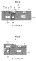
FIG. 4 is a drawing showing a general outline of a substrate holder used in a film formation apparatus according to a first embodiment of the present invention; -
FIG. 5 is a drawing showing a general outline of a substrate holder used in a film formation apparatus according to a second embodiment of the present invention; -
FIG. 6 is a drawing showing a wafer on which a metal film is formed in the film formation apparatus inFIG. 6 ; -
FIG. 7 is a drawing showing a general outline of a substrate holder used in a film formation apparatus according to a third embodiment of the present invention; and -
FIG. 8 is a drawing showing a general outline of a substrate holder used in a film formation apparatus according to a fourth embodiment of the present invention. -
FIG. 1 shows a configuration of afilm formation apparatus 10 according to an embodiment of the present invention. - As shown in
FIG. 1 , thefilm formation apparatus 10 includes aprocessing container 12 and anevacuation system 11 for evacuating theprocessing container 12. Theprocessing container 12 includes asubstrate holder 13 for holding a target substrate "W" and agate bulb 12G formed on theprocessing container 12 for putting in and taking out the target substrate "W". - The
substrate holder 13 includes a built-in heater to maintain the target substrate "W" at a desired temperature by driving the heater through adrive line 13A. - The
evacuation system 11 includes a turbomolecular pump 11A and adry pump 11B in series. Nitrogen gas is supplied to the turbomolecular pump 11A through abulb 11b. - A
variable conductance valve 11a is between theprocessing container 12 and the turbomolecular pump 11A to maintain the entire pressure in theprocessing container 12 at a constant pressure. Further, in the film formation apparatus 1, an evacuation route 11C as a bypass of the turbomolecular pump 11A is provided so that theprocessing container 12 is roughly pumped by thedry pump 11B. Avalve 11c is for the evacuation route 11C, and another valve 11d is on the downstream side of the turbomolecular pump 11A. - A source in a gas phase for forming a film is supplied from a
source supply system 14 including abubbler 14A to theprocessing container 12 through agas introduction line 14B. - In the example of the figure, Ru3(CO)12, which is a Ru-carbonyl compound, is stored in the
bubbler 14A. CO gas is supplied as bubbling gas to thebubbler 14A through abubbling gas line 14a on which an MFC (Mass Flow Controller) 14b is provided. As a result, evaporated Ru3(CO)12 along with CO carrier gas through aline 14d on which aline MFC 14c is provided are supplied to theprocessing container 12 through thegas introduction line 14B. - Further, the
source supply system 14 of the configuration inFIG. 1 includes aline 14f on whichvalves MFC 14e are provided and that supplies inert gas, such as Ar, to be added to the Ru3(CO)12 source gas to be supplied to theprocessing container 12 through theline 14B. - Further, the
film formation apparatus 10 includes acontrol device 10A for controlling theprocessing container 12, theevacuation system 11, and thesource supply system 14. -
FIG. 2 is a drawing showing where a Ru film is deposited on a wafer "W" supported on thesubstrate holder 13. More specifically,FIG. 2 shows an edge portion of the wafer "W" in detail. - As shown in
FIG. 2 , the wafer "W" is positioned in a concave portion formed on a surface of thesubstrate holder 13 shown inFIG. 1 in a manner so that a rounded edge portion of the wafer "W" faces and is separated from a side wall surface of the concave portion by a slight distance of, for example, 0.5 mm to 1 mm. - In the
film formation apparatus 10 ofFIG. 1 , the gas-phase source of Ru3(CO)12 bubbled in thebubbler 14A by the CO gas through theline 14a are combined with high-concentration CO carrier gas through theline 14d, and the combined gas is supplied to theprocessing container 12. On the surface of the target substrate "W", the source of Ru3(CO)12 is decomposed by releasing CO and ametal Ru film 21 is deposited on the wafer "W" in accordance with the following reaction formula:
Ru3(CO)12 → 3Ru + 12CO (1)
- This reaction formula shows that the
metal Ru film 21 is deposited on a surface of thesubstrate holder 13. - When the CO partial pressure in the atmosphere is low, the reaction in Formula (1) proceeds in the right (arrow) direction so that the separation of Ru is accelerated. On the other hand, when the CO partial pressure in the atmosphere is high, the reaction proceeding to the right is impeded. This characteristic is also applied to a case where a metal film using a metal carbonyl source such as W, Ni, Co, Rh, Re, and Cr is formed.
- This characteristic shows that the reaction resulting in a deposit of the metal film using such a metal carbonyl source can be adjusted when the CO partial pressure in the atmosphere can be adjusted. To make use of this characteristic, in the
film formation apparatus 10 inFIG. 1 , CO gas is used as the carrier gas to increase the CO partial pressure while the metal carbonyl source is being transferred, thereby better controlling the separation of the metal carbonyl source and the deposit of the metal film in its flow path. - The deposit and separation from the Ru3(CO)12 source as shown in the above Formula (1) may also occur in the
processing container 12 including a peripheral portion of the wafer "W" on thesubstrate holder 13. The inventors of the present invention have discovered in fundamental research of the present invention that, in an area along the peripheral portion of the wafer in the concave portion formed on the surface of thesubstrate holder 13 as shown inFIG. 2 , when the distance between the peripheral portion of the wafer and an inner wall of the concave portion is adequate, the released CO gas from the decomposition of Ru3(CO)12 accumulates, and the CO concentration is locally increased; accordingly, the formation of the Ru film is controlled especially on the inclined slope on the lower side of the peripheral portion of the target substrate as pointed to by an arrow "A". - The present invention is made based on the discovered fact and may provide a film formation apparatus and a film formation method capable of reliably controlling the depositing of the metal film on the peripheral portion of the wafer when a metal film is being formed on the wafer by the decomposition of the metal carbonyl source.
-
FIG. 3 shows the relationships between the deposition rate of the Ru film formed by the decomposition of such a Ru3(CO)12 source and the CO partial pressure in atmosphere when the substrate temperatures are 160 °C, 180 °C, 200 °C, and 250 °C as a result of the fundamental research of the present invention. - As shown in
FIG. 3 , at each substrate temperature, the Ru deposit starts when the CO partial pressure is low, and the lower the CO partial pressure becomes, the more the deposition rate of the Ru film increases. - For example, at 180 °C of the substrate temperature, when the CO partial pressure in the atmosphere is equal to or greater than 130 Pa, the Ru film is not formed (value of the deposition rate is zero); and, on the other hand, when the CO partial pressure in atmosphere is less than 130 Pa, the film forming process starts to deposit the Ru film at a finite deposition rate.
- Further, as the relationships in
FIG. 3 show, at 50 mTorr of the CO partial pressure, when the temperature is 200 °C, the Ru film is deposited at a first deposition rate "DR1" which is approximately 3.9 nm/minute. In this case, when the free diffusion of the CO gas released by the above reaction is impeded, as shown by the bold arrow, the CO partial pressure increases locally near the portion where the Ru film is formed. For example, the CO partial pressure is locally increased to approximately 130 mTorr, the deposition rate of the metal Ru film according to Formula (1) decreases to a second deposition rate "DR2" which is approximately 2.4 nm/minute at the same temperature of 200 °C. - Further, in the atmosphere where the CO partial pressure is locally increased to approximately 130 mTorr, when the temperature of the wafer is maintained at a lower temperature, for example 180 °C, as shown in
FIG. 3 , the deposition rate "R3" of the metal Ru film according to Formula (1) becomes zero, thereby controlling the depositing of the metal Ru film on the wafer. - Therefore, according to an embodiment of the present invention, there is provided a structure capable of controlling the free diffusion of the CO gas released as a reaction product when the metal Ru film is bing deposited according to Formula (1) along the peripheral portion of the target substrate that is the wafer. Further, the temperature of the structure is set higher than that of the wafer, thereby controlling the depositing of the metal film on the peripheral portion of the wafer.
-
FIG. 4 schematically shows a configuration of asubstrate holder 23 according to a first embodiment of the present invention used in thefilm formation apparatus 10 inFIG. 1 . - As shown in
FIG. 4 , thesubstrate holder 23 includes a supportingsection 23A having substantially the same diameter of the wafer "W" to sustain the wafer "W" and a ring-shapedtemperature control section 23B outside and in contact with the supportingsection 23A. The supportingsection 23A is heated to the temperature of "T1" by a first heater (not shown) buried in the supportingsection 23A. Thetemperature control section 23B is heated to the temperature of "T3" which is higher than that of "T1" (T1<T3) by a second heater (not shown). - Further, outside of the
temperature control section 23B, an outerperipheral member 23C is formed so as to constitute an outer peripheral portion of thesubstrate holder 23. Still further, outside of the outerperipheral member 23C, acover ring 23D is provided in a manner so that the cover ring covers the side wall surface and the upper surface of the outerperipheral member 23C and the most of the upper surface of thetemperature control section 23B. - At the inner side end portion of the
cover ring 23D, aninner wall surface 23d is formed. Theinner wall surface 23d faces the side wall surface of the wafer "W" and is separated from the outer peripheral surface of the wafer "W" by a distance "D" of 0.5 mm, and has a height of, for example, 1 mm. As a result, asmall space 23S having a ratio of height to width (aspect ratio) of approximately 2 and in communication with a process space above the wafer "W" is formed between the outer peripheral surface of the wafer "W" and thecover ring 23D. - Further, the
cover ring 23D includes amember 23e engaged with the upper surface of the outerperipheral member 23C, so that a gap "d" having a size from 0.05 mm to 0.5 mm is formed between the upper surface of the outerperipheral member 23C and the bottom surface of thecover ring 23D. - In this configuration, the wafer "W" supported on the supporting
section 23A having a temperature of "T1" is maintained at the temperature of "T2" which is lower than that of "T1" because heat of the wafer "W" is transferred to the process space. On the other hand, as described above, thetemperature control section 23B is maintained at the temperature of "T3" which is higher than that of "T1". As a result, the relationships among the temperatures "T1", "T2", and "T3" are expressed by the inequality T3>T1>T2. - It should be noted that the outer
peripheral member 23C is at the temperature of "T4" (T4≦T2) which is lower that that of "T1" heated by a third heater (not shown) buried in outerperipheral member 23C, which assists in ensuring that thetemperature control section 23B is maintained at the desired high temperature "T3" by the second heater. - For example, when the temperature "T1" of the supporting
section 23A is 225 °C, the temperature "T2" of the wafer "W" is maintained at 198 °C. - Now, referring to the relationships in
FIG. 3 , when the temperature of thetemperature control section 23B is, for example, 250 °C which is higher than the temperature "T1", the decomposition of the Ru3(CO)12 source is accelerated in thespace 23S along the peripheral portion of the wafer "W", and the diffusion of the CO released as the reaction product of the decomposition is impeded. As a result, the CO partial pressure in thespace 23S is locally increased, and accordingly, the deposit of the metal Ru film is controlled on the side wall surface of the wafer "W" maintained at the low temperature "T1". -
FIG. 5 schematically shows a configuration of asubstrate holder 33 according to a second embodiment of the present invention. In the figure, the same reference numerals are used for the corresponding elements described above and the description of the elements is herein omitted. - As shown in
FIG. 5 , in thesubstrate holder 33, thetemperature control section 23B is not included between the supportingsection 23A and the outerperipheral member 23C, and the outerperipheral member 23C contiguously covers the outer side of the supportingsection 23A. - Further, in the configuration in
FIG. 5 , thecover ring 23D is heated to a temperature "T3" which is higher than the temperature "T1" of the supportingsection 23A by a heater (not shown) buried in thecover ring 23D. - The
cover ring 23D includes its end portion which covers the peripheral portion of the upper surface of the wafer "W" in a ring shape. As a result, a space is formed having a width of "d" between the end portion and the upper surface of the wafer "W" and in communication with the process space where the wafer "W" is exposed. - In this configuration as well, in the wafer peripheral portion "Wa" covered by the
cover ring 23D, by increasing the temperature of the surface of thecover ring 23D facing the surface of the wafer up to a temperature higher than temperature "T1" of the wafer main portion, the decomposition of the Ru3(CO)12 source is accelerated on the surface of thecover ring 23D, thereby locally increasing the CO concentration in the space. As a result, it becomes possible to control the depositing of the Ru film on the wafer peripheral potion "Wa" of the target wafer "W" as shown inFIG. 6 . -
FIG. 7 schematically shows a configuration of asubstrate holder 43 according to a third embodiment of the present invention. In the figure, the same reference numerals are used for the corresponding elements described above and the description of the elements is herein omitted. - As shown in
FIG. 7 , the upper surface of the wafer "W" is held by aclamp ring 23 that is movably provided in up and down directions. Theclamp ring 23E is in engaged with the wafer in its lowered position as shown inFIG. 7 . When theclamp ring 23E is lifted up to its higher position, the wafer "W" is released. - When the
clamp ring 23E is positioned at its lowered position, theclamp ring 23E is in contact with aheat source 23F that is formed in a ring shape outside the supportingsection 23A and that is maintained at the temperature "T5" by a heater RA. As a result, theclamp ring 23E is heated to the temperature "T3" (T3<T5). - Further, in the configuration in
FIG. 7 , the supportingsection 23A is heated to the temperature "T1" (T2<T1<T3) by a heater RA. - According to the configuration, the
heat source 23F may be fixed and the configuration of theclamp ring 23E may be simplified. - It should be noted that, in the configuration of
FIG. 7 , theclamp ring 23E may be separated from the surface of the wafer "W" when theclamp ring 23E is positioned at its lowered position. By doing this, the configuration may become substantially equal to that ofFIG. 5 . -
FIG. 8 schematically shows a configuration of asubstrate holder 53 according to a fourth embodiment of the present invention. - As shown in
FIG. 8 , the configuration of thesubstrate holder 53 is substantially equal to that shown inFIG. 2 . The wafer "W" is positioned in the concave portion formed on thesubstrate holder 53 in a manner so that the wafer "W" is separated from the inner wall surface of the concave portion by a distance "D" of 0.5 mm. As a result, a ring-shapedspace 13D having a ratio of width to depth of approximately 2 and in communication with the process space above the wafer "W" is formed outside the peripheral portion of the wafer "W". - In the configuration of
FIG. 8 , there is no high temperature section in thesubstrate holder 53. However, by forming the ring shaped space as shown inFIG. 8 , it becomes possible to control the diffusion of the CO gas released by the composition of the metal carbonyl source in this space, thereby controlling the depositing of the metal Ru film on the outer peripheral area of the wafer "W". - In each of the embodiments, an example of forming the metal Ru film from the Ru3(CO)12 source is described. However, the embodiments of the present invention are not limited to the specific examples described above. For example, W film, Ni film, Mo film, Co film, Rh film, Re film, and Cr film may be formed from W(CO)6, Ni(CO)4, Mo(CO)6, Co2(CO)6, Rh4(CO)12, Re2(CO)10, and Cr(CO)6, respectively, as other metal carbonyl sources within a scope of the present invention.
- Although the invention has been described with respect to a specific embodiment for a complete and clear disclosure, the appended claims are not to be thus limited but are to be construed as embodying all modifications and alternative constructions that may occur to one skilled in the art that fairly fall within the basic teachings herein set forth.
- The present application is based on and claims the benefit of priority of Japanese Patent Application No.
2007-085022, filed on March 28, 2007
Claims (14)
- A film formation method for depositing a metal film on a target substrate by supplying a metal carbonyl source in a gas phase to a surface of the target substrate and decomposing the source near the surface of the target substrate, the method comprising:a step of preferentially decomposing the metal carbonyl source in an area near the outer peripheral portion of the target substrate when the metal film is being deposited on the surface of the target substrate; whereina CO concentration in atmosphere is increased locally near the outer peripheral portion of the target substrate, and the depositing of the metal film on the outer peripheral portion is better controlled.
- The film formation method according to claim 1, wherein
the step of preferentially decomposing the metal carbonyl source deposited in an area near the outer peripheral portion of the target substrate includes
a step of increasing the temperature of the area near the outer peripheral portion of the target substrate up to a temperature higher than that of the surface of the target substrate. - The film formation method according to claim 1, wherein
the step of preferentially decomposing the metal carbonyl source deposited in an area near the outer peripheral portion of the target substrate includes
a step of forming a second atmospheric space near the outer peripheral portion, the second atmospheric space being in communication with a first atmospheric space facing a main portion of the target substrate and having a volume smaller than that of the first atmospheric space. - The film formation method according to claim 3, wherein
the step of forming the second atmospheric space includes
a step of placing the target substrate on a substrate holder on which a concave portion is formed, so that an outer peripheral surface of the target substrate faces an inner peripheral surface of the concave portion. - The film formation method according to claim 3, wherein
the step of forming the second atmospheric space includes
a step of placing a cover member to cover the outer peripheral portion of the target substrate. - The film formation method according to claim 2, wherein
the step of increasing the temperature of the area near the outer peripheral portion of the target substrate up to a temperature higher than that of the surface of the target substrate includes
a step of placing a cover member to cover the outer peripheral portion of the target substrate, and increasing the temperature of the cover member up to a temperature higher than that of the surface of the target substrate. - A film formation apparatus comprising
a processing container including:a substrate holder for supporting a target substrate;an evacuation system for evacuating the processing container;a first gas supply system for supplying a gas of metal carbonyl source to the processing container; anda second gas supply system for supplying a gas for controlling the decomposition of the metal carbonyl source in the processing container, whereinthe substrate holder has sizes corresponding to an outer diameter of the target substrate and includes a supporting section for sustaining the target substrate and a temperature control section contiguously surrounding the supporting section, andthe temperature control section is maintained at a temperature higher than that of the supporting section when the metal film is being formed on the target substrate by the decomposition of the metal carbonyl source. - The film formation apparatus according to claim 7, wherein
the temperature control section has a heating zone different from that of the supporting section and a surface in substantially the same plane as a surface of the supporting section. - The film formation apparatus according to claim 7, wherein
the temperature control section includes a facing surface facing the outer peripheral surface of the target substrate on the supporting section, and
a small space is formed between the facing surface and the outer peripheral surface, the small space being in communication with a process space in the processing container and having a volume smaller than that of the process space. - The film formation apparatus according to claim 9, wherein
the facing surface is formed in a manner so that the facing surface is separated from the outer peripheral surface by a distance from 0.5 mm to 1 mm. - The film formation apparatus according to claim 7, wherein
the temperature control section includes a cover member covering and separated from the outer peripheral surface of the target substrate, and
the cover member is maintained at a temperature higher than that of the supporting section when the metal film is being formed. - The film formation apparatus according to claim 11, wherein
the cover member is placed in a manner so that the cover member is separated from the outer peripheral surface by a distance of 0.5 mm to 1 mm when the metal film is being formed. - The film formation apparatus according to claim 7, wherein
the temperature control section includes a clamp ring covering and in contact with the outer peripheral surface of the target substrate, and
the clamp ring is maintained at a temperature higher than that of the supporting section when the metal film is being formed. - The film formation apparatus according to claim 13, wherein
the clamp ring is movably provided between a first position to be in contact with the outer peripheral surface of the target substrate and a second position to be separated from the outer peripheral surface, and in contact with a heat source at the first position to be heated to a temperature higher than that of the supporting section.
Applications Claiming Priority (2)
| Application Number | Priority Date | Filing Date | Title |
|---|---|---|---|
| JP2007085022A JP5236197B2 (en) | 2007-03-28 | 2007-03-28 | Film forming method and film forming apparatus |
| PCT/JP2008/052757 WO2008117590A1 (en) | 2007-03-28 | 2008-02-19 | Method of forming film and film forming apparatus |
Publications (2)
| Publication Number | Publication Date |
|---|---|
| EP2067875A1 true EP2067875A1 (en) | 2009-06-10 |
| EP2067875A4 EP2067875A4 (en) | 2011-09-07 |
Family
ID=39788329
Family Applications (1)
| Application Number | Title | Priority Date | Filing Date |
|---|---|---|---|
| EP08711581A Withdrawn EP2067875A4 (en) | 2007-03-28 | 2008-02-19 | METHOD AND APPARATUS FOR FILM FORMATION |
Country Status (7)
| Country | Link |
|---|---|
| US (1) | US8277889B2 (en) |
| EP (1) | EP2067875A4 (en) |
| JP (1) | JP5236197B2 (en) |
| KR (1) | KR101062586B1 (en) |
| CN (1) | CN101542016B (en) |
| TW (1) | TWI440092B (en) |
| WO (1) | WO2008117590A1 (en) |
Families Citing this family (6)
| Publication number | Priority date | Publication date | Assignee | Title |
|---|---|---|---|---|
| JP2014055342A (en) * | 2012-09-14 | 2014-03-27 | Hitachi High-Technologies Corp | Film deposition apparatus |
| CN105164307B (en) * | 2013-04-30 | 2017-06-27 | 东京毅力科创株式会社 | Film formation device |
| TWI491758B (en) * | 2013-05-14 | 2015-07-11 | 世界中心科技股份有限公司 | Deposition apparatus for optoelectronic semiconductor processes and its cover |
| KR102181233B1 (en) * | 2013-07-19 | 2020-11-23 | 삼성디스플레이 주식회사 | Plasma enhanced chemical vapor deposition device and display appratus using the same |
| JP2015160963A (en) * | 2014-02-26 | 2015-09-07 | 東京エレクトロン株式会社 | Ruthenium film forming method, film forming apparatus, and semiconductor device manufacturing method |
| JP7767691B2 (en) * | 2022-07-13 | 2025-11-12 | 株式会社デンソー | Semiconductor wafer manufacturing equipment |
Family Cites Families (40)
| Publication number | Priority date | Publication date | Assignee | Title |
|---|---|---|---|---|
| US2375944A (en) * | 1939-01-24 | 1945-05-15 | Quentin Alberto | Method of tempering glass articles |
| US2309290A (en) * | 1939-11-25 | 1943-01-26 | Hartford Empire Co | Cooling nozzle for tempering hollow glassware |
| US2338071A (en) * | 1941-05-22 | 1943-12-28 | Hartford Empire Co | Apparatus for tempering glass bottles and like articles |
| US2561529A (en) * | 1942-08-10 | 1951-07-24 | Emhart Mfg Co | Apparatus for handling and tempering glassware |
| US2539159A (en) * | 1944-02-26 | 1951-01-23 | Hartford Empire Co | Method of treating annealed glassware before complete colling thereof |
| US2484925A (en) * | 1947-06-04 | 1949-10-18 | Corning Glass Works | Tempering apparatus |
| US2982052A (en) * | 1955-07-28 | 1961-05-02 | British Hartford Fairmont Ltd | Lehrs for glassware |
| US3150949A (en) * | 1958-05-20 | 1964-09-29 | Owens Illinois Glass Co | Method and apparatus for direct loading of machine-made articles into a lehr |
| US3107086A (en) * | 1958-05-20 | 1963-10-15 | Owens Illinois Glass Co | Direct loading lehr for machine-made glass articles |
| US3259481A (en) * | 1963-02-28 | 1966-07-05 | Emhart Corp | Glassware annealing lehr |
| US3378243A (en) * | 1965-10-24 | 1968-04-16 | Sunbeam Corp | Lehr with transverse temperature control |
| BE788045A (en) * | 1971-11-10 | 1973-02-26 | Bowman E W | METHOD AND APPARATUS FOR RECEIVING GLASSWARE OR ANALOGUE ARTICLES |
| US3855966A (en) * | 1973-11-30 | 1974-12-24 | Wheaton Industries | Universal chucking mechanism |
| US3994711A (en) * | 1975-09-15 | 1976-11-30 | Mcmaster Harold | Glass tempering system including oscillating roller furnace |
| US4162907A (en) * | 1978-04-07 | 1979-07-31 | Frank Anderson | Glass sheet manufacturing method and apparatus |
| US4481025A (en) * | 1981-12-15 | 1984-11-06 | Vitro Tec Fideicomiso | Glass annealing lehr |
| FR2634274B1 (en) * | 1988-07-13 | 1990-10-19 | Sleever Int | PROCESS FOR CONTROLLING THE TEMPERATURE IN AN OVEN-TUNNEL OPEN AT ITS TWO ENDS, AND DEVICE FOR IMPLEMENTING THE PROCESS |
| DE3913571C1 (en) * | 1989-04-25 | 1990-07-26 | Vegla Vereinigte Glaswerke Gmbh, 5100 Aachen, De | |
| JPH043926A (en) * | 1990-04-20 | 1992-01-08 | Sony Corp | Manufacture of semiconductor device |
| US5855687A (en) * | 1990-12-05 | 1999-01-05 | Applied Materials, Inc. | Substrate support shield in wafer processing reactors |
| US5337537A (en) * | 1992-12-28 | 1994-08-16 | Soughan John J | Granulable container means and method |
| JPH0885875A (en) * | 1994-09-19 | 1996-04-02 | Hitachi Ltd | Plasma processing device |
| JPH08302474A (en) * | 1995-04-28 | 1996-11-19 | Anelva Corp | Heating equipment for CVD equipment |
| US6221166B1 (en) * | 2000-06-07 | 2001-04-24 | Simplus Systems Corporation | Multi-thermal zone shielding apparatus |
| US7694532B1 (en) * | 2002-09-19 | 2010-04-13 | Boaz Premakaran T | System and method for tempering glass containers |
| US7427426B2 (en) | 2002-11-06 | 2008-09-23 | Tokyo Electron Limited | CVD method for forming metal film by using metal carbonyl gas |
| JP4126219B2 (en) * | 2002-11-06 | 2008-07-30 | 東京エレクトロン株式会社 | Deposition method |
| US7270848B2 (en) * | 2004-11-23 | 2007-09-18 | Tokyo Electron Limited | Method for increasing deposition rates of metal layers from metal-carbonyl precursors |
| US8435351B2 (en) * | 2004-11-29 | 2013-05-07 | Tokyo Electron Limited | Method and system for measuring a flow rate in a solid precursor delivery system |
| JP2006274316A (en) * | 2005-03-28 | 2006-10-12 | Hitachi Kokusai Electric Inc | Substrate processing equipment |
| JP2007085022A (en) | 2005-09-20 | 2007-04-05 | Ebata Kk | Invert member and manhole |
| US20070234955A1 (en) * | 2006-03-29 | 2007-10-11 | Tokyo Electron Limited | Method and apparatus for reducing carbon monoxide poisoning at the peripheral edge of a substrate in a thin film deposition system |
| US7892358B2 (en) * | 2006-03-29 | 2011-02-22 | Tokyo Electron Limited | System for introducing a precursor gas to a vapor deposition system |
| US7858522B2 (en) * | 2006-03-29 | 2010-12-28 | Tokyo Electron Limited | Method for reducing carbon monoxide poisoning in a thin film deposition system |
| US20070231489A1 (en) * | 2006-03-29 | 2007-10-04 | Tokyo Electron Limited | Method for introducing a precursor gas to a vapor deposition system |
| US7867560B2 (en) * | 2007-03-28 | 2011-01-11 | Tokyo Electron Limited | Method for performing a vapor deposition process |
| US7794788B2 (en) * | 2007-03-28 | 2010-09-14 | Tokyo Electron Limited | Method for pre-conditioning a precursor vaporization system for a vapor deposition process |
| US7763311B2 (en) * | 2007-03-28 | 2010-07-27 | Tokyo Electron Limited | Method for heating a substrate prior to a vapor deposition process |
| US8650908B2 (en) * | 2010-05-25 | 2014-02-18 | Emhart Glass S.A. | Post-manufacture glass container thermal strengthening on a conveyor |
| US8839644B2 (en) * | 2010-05-25 | 2014-09-23 | Emhart Glass S.A. | Post-manufacture glass container thermal strengthening method |
-
2007
- 2007-03-28 JP JP2007085022A patent/JP5236197B2/en active Active
-
2008
- 2008-02-19 CN CN2008800001488A patent/CN101542016B/en active Active
- 2008-02-19 WO PCT/JP2008/052757 patent/WO2008117590A1/en not_active Ceased
- 2008-02-19 KR KR1020087024696A patent/KR101062586B1/en active Active
- 2008-02-19 US US12/443,487 patent/US8277889B2/en active Active
- 2008-02-19 EP EP08711581A patent/EP2067875A4/en not_active Withdrawn
- 2008-03-27 TW TW097111065A patent/TWI440092B/en active
Also Published As
| Publication number | Publication date |
|---|---|
| US20100075035A1 (en) | 2010-03-25 |
| EP2067875A4 (en) | 2011-09-07 |
| TW200849398A (en) | 2008-12-16 |
| WO2008117590A1 (en) | 2008-10-02 |
| CN101542016B (en) | 2011-08-24 |
| JP5236197B2 (en) | 2013-07-17 |
| JP2008240108A (en) | 2008-10-09 |
| KR101062586B1 (en) | 2011-09-06 |
| CN101542016A (en) | 2009-09-23 |
| US8277889B2 (en) | 2012-10-02 |
| KR20080106572A (en) | 2008-12-08 |
| TWI440092B (en) | 2014-06-01 |
Similar Documents
| Publication | Publication Date | Title |
|---|---|---|
| US9048294B2 (en) | Methods for depositing manganese and manganese nitrides | |
| US9076661B2 (en) | Methods for manganese nitride integration | |
| TWI394858B (en) | Method for depositing a tungsten film having reduced resistivity and improved surface morphology | |
| US10879081B2 (en) | Methods of reducing or eliminating defects in tungsten film | |
| TWI687994B (en) | Methods for etching via atomic layer deposition (ald) cycles | |
| US20080241575A1 (en) | Selective aluminum doping of copper interconnects and structures formed thereby | |
| US20200083098A1 (en) | Embedding Method and Processing System | |
| US20130140698A1 (en) | Doped Tantalum Nitride for Copper Barrier Applications | |
| KR20170017963A (en) | Tungsten film forming method | |
| US8277889B2 (en) | Film formation method and film formation apparatus | |
| US20200098627A1 (en) | Embedding method and processing system | |
| KR101217393B1 (en) | Film forming method, plasma processing apparatus and storage medium | |
| KR101923807B1 (en) | Cu WIRING MANUFACTURING METHOD AND Cu WIRING MANUFACTURING SYSTEM | |
| US20170025308A1 (en) | Method of cleaning bottom of via hole and method of manufacturing semiconductor device | |
| TWI609095B (en) | Method for manganese nitride integration | |
| US20120040085A1 (en) | METHOD FOR FORMING Cu FILM AND STORAGE MEDIUM | |
| US20250285918A1 (en) | Methods of depositing iridium-containing films for semiconductor devices | |
| US20060068588A1 (en) | Low-pressure deposition of ruthenium and rhenium metal layers from metal carbonyl precursors | |
| JP2001345379A (en) | Semiconductor device and method of manufacturing the same | |
| CN118786517A (en) | Low resistance Mo deposition for logic source/drain contacts | |
| JP2002110783A (en) | Semiconductor substrate, method of manufacturing semiconductor device, and semiconductor device |
Legal Events
| Date | Code | Title | Description |
|---|---|---|---|
| PUAI | Public reference made under article 153(3) epc to a published international application that has entered the european phase |
Free format text: ORIGINAL CODE: 0009012 |
|
| 17P | Request for examination filed |
Effective date: 20090323 |
|
| AK | Designated contracting states |
Kind code of ref document: A1 Designated state(s): AT BE BG CH CY CZ DE DK EE ES FI FR GB GR HR HU IE IS IT LI LT LU LV MC MT NL NO PL PT RO SE SI SK TR |
|
| AX | Request for extension of the european patent |
Extension state: AL BA MK RS |
|
| DAX | Request for extension of the european patent (deleted) | ||
| RBV | Designated contracting states (corrected) |
Designated state(s): BE DE IT NL |
|
| A4 | Supplementary search report drawn up and despatched |
Effective date: 20110805 |
|
| RIC1 | Information provided on ipc code assigned before grant |
Ipc: C23C 16/458 20060101ALI20110801BHEP Ipc: H01L 21/285 20060101ALI20110801BHEP Ipc: C23C 16/16 20060101AFI20110801BHEP |
|
| STAA | Information on the status of an ep patent application or granted ep patent |
Free format text: STATUS: THE APPLICATION HAS BEEN WITHDRAWN |
|
| 18W | Application withdrawn |
Effective date: 20140306 |