EP2065950A2 - Organic electroluminescent device - Google Patents
Organic electroluminescent device Download PDFInfo
- Publication number
- EP2065950A2 EP2065950A2 EP09003786A EP09003786A EP2065950A2 EP 2065950 A2 EP2065950 A2 EP 2065950A2 EP 09003786 A EP09003786 A EP 09003786A EP 09003786 A EP09003786 A EP 09003786A EP 2065950 A2 EP2065950 A2 EP 2065950A2
- Authority
- EP
- European Patent Office
- Prior art keywords
- electrode
- electroluminescent
- film
- organic
- generation layer
- Prior art date
- Legal status (The legal status is an assumption and is not a legal conclusion. Google has not performed a legal analysis and makes no representation as to the accuracy of the status listed.)
- Granted
Links
Images



Classifications
-
- H—ELECTRICITY
- H10—SEMICONDUCTOR DEVICES; ELECTRIC SOLID-STATE DEVICES NOT OTHERWISE PROVIDED FOR
- H10K—ORGANIC ELECTRIC SOLID-STATE DEVICES
- H10K50/00—Organic light-emitting devices
- H10K50/80—Constructional details
- H10K50/805—Electrodes
-
- H—ELECTRICITY
- H10—SEMICONDUCTOR DEVICES; ELECTRIC SOLID-STATE DEVICES NOT OTHERWISE PROVIDED FOR
- H10K—ORGANIC ELECTRIC SOLID-STATE DEVICES
- H10K50/00—Organic light-emitting devices
- H10K50/10—OLEDs or polymer light-emitting diodes [PLED]
- H10K50/11—OLEDs or polymer light-emitting diodes [PLED] characterised by the electroluminescent [EL] layers
-
- H—ELECTRICITY
- H10—SEMICONDUCTOR DEVICES; ELECTRIC SOLID-STATE DEVICES NOT OTHERWISE PROVIDED FOR
- H10K—ORGANIC ELECTRIC SOLID-STATE DEVICES
- H10K50/00—Organic light-emitting devices
- H10K50/10—OLEDs or polymer light-emitting diodes [PLED]
- H10K50/11—OLEDs or polymer light-emitting diodes [PLED] characterised by the electroluminescent [EL] layers
- H10K50/125—OLEDs or polymer light-emitting diodes [PLED] characterised by the electroluminescent [EL] layers specially adapted for multicolour light emission, e.g. for emitting white light
- H10K50/13—OLEDs or polymer light-emitting diodes [PLED] characterised by the electroluminescent [EL] layers specially adapted for multicolour light emission, e.g. for emitting white light comprising stacked EL layers within one EL unit
-
- H—ELECTRICITY
- H10—SEMICONDUCTOR DEVICES; ELECTRIC SOLID-STATE DEVICES NOT OTHERWISE PROVIDED FOR
- H10K—ORGANIC ELECTRIC SOLID-STATE DEVICES
- H10K50/00—Organic light-emitting devices
- H10K50/10—OLEDs or polymer light-emitting diodes [PLED]
- H10K50/17—Carrier injection layers
-
- H—ELECTRICITY
- H10—SEMICONDUCTOR DEVICES; ELECTRIC SOLID-STATE DEVICES NOT OTHERWISE PROVIDED FOR
- H10K—ORGANIC ELECTRIC SOLID-STATE DEVICES
- H10K50/00—Organic light-emitting devices
- H10K50/10—OLEDs or polymer light-emitting diodes [PLED]
- H10K50/19—Tandem OLEDs
-
- H—ELECTRICITY
- H10—SEMICONDUCTOR DEVICES; ELECTRIC SOLID-STATE DEVICES NOT OTHERWISE PROVIDED FOR
- H10K—ORGANIC ELECTRIC SOLID-STATE DEVICES
- H10K50/00—Organic light-emitting devices
- H10K50/80—Constructional details
- H10K50/805—Electrodes
- H10K50/81—Anodes
-
- H—ELECTRICITY
- H10—SEMICONDUCTOR DEVICES; ELECTRIC SOLID-STATE DEVICES NOT OTHERWISE PROVIDED FOR
- H10K—ORGANIC ELECTRIC SOLID-STATE DEVICES
- H10K50/00—Organic light-emitting devices
- H10K50/80—Constructional details
- H10K50/805—Electrodes
- H10K50/82—Cathodes
-
- H—ELECTRICITY
- H10—SEMICONDUCTOR DEVICES; ELECTRIC SOLID-STATE DEVICES NOT OTHERWISE PROVIDED FOR
- H10K—ORGANIC ELECTRIC SOLID-STATE DEVICES
- H10K50/00—Organic light-emitting devices
- H10K50/80—Constructional details
- H10K50/84—Passivation; Containers; Encapsulations
-
- H—ELECTRICITY
- H10—SEMICONDUCTOR DEVICES; ELECTRIC SOLID-STATE DEVICES NOT OTHERWISE PROVIDED FOR
- H10K—ORGANIC ELECTRIC SOLID-STATE DEVICES
- H10K71/00—Manufacture or treatment specially adapted for the organic devices covered by this subclass
- H10K71/841—Applying alternating current [AC] during manufacturing or treatment
-
- F—MECHANICAL ENGINEERING; LIGHTING; HEATING; WEAPONS; BLASTING
- F21—LIGHTING
- F21Y—INDEXING SCHEME ASSOCIATED WITH SUBCLASSES F21K, F21L, F21S and F21V, RELATING TO THE FORM OR THE KIND OF THE LIGHT SOURCES OR OF THE COLOUR OF THE LIGHT EMITTED
- F21Y2115/00—Light-generating elements of semiconductor light sources
- F21Y2115/10—Light-emitting diodes [LED]
- F21Y2115/15—Organic light-emitting diodes [OLED]
-
- H—ELECTRICITY
- H10—SEMICONDUCTOR DEVICES; ELECTRIC SOLID-STATE DEVICES NOT OTHERWISE PROVIDED FOR
- H10K—ORGANIC ELECTRIC SOLID-STATE DEVICES
- H10K50/00—Organic light-emitting devices
- H10K50/10—OLEDs or polymer light-emitting diodes [PLED]
- H10K50/18—Carrier blocking layers
-
- Y—GENERAL TAGGING OF NEW TECHNOLOGICAL DEVELOPMENTS; GENERAL TAGGING OF CROSS-SECTIONAL TECHNOLOGIES SPANNING OVER SEVERAL SECTIONS OF THE IPC; TECHNICAL SUBJECTS COVERED BY FORMER USPC CROSS-REFERENCE ART COLLECTIONS [XRACs] AND DIGESTS
- Y10—TECHNICAL SUBJECTS COVERED BY FORMER USPC
- Y10S—TECHNICAL SUBJECTS COVERED BY FORMER USPC CROSS-REFERENCE ART COLLECTIONS [XRACs] AND DIGESTS
- Y10S428/00—Stock material or miscellaneous articles
- Y10S428/917—Electroluminescent
Definitions
- the present invention relates to an organic electroluminescent device having an organic compound layer that generates light upon application of an electric field. More particularly, the present invention relates to an organic electroluminescent device that emits light using alternating current bias.
- organic compounds Compared to inorganic compounds, organic compounds have more various material systems and possibilities for synthesizing organic materials to have advanced various functions through appropriate molecular design. Further, things made from the organic compound have characteristics of being flexible, and moreover, having workability by polymerization. In light of these advantages, in recent years, the technique of photonics and electronics employing functional organic materials have been attracted attention.
- photonics utilizing optical properties of organic materials has already played an important role in contemporary industrial technology.
- photosensitive materials such as a photoresist have become indispensable for a photolithography technique that is used for the micro machining of semiconductors.
- organic compounds themselves have properties of light absorption and light emission caused by the light absorption (fluorescence or phosphorescence), they are also well suited to light emitting materials for laser pigments or the like.
- organic compounds do not have carriers themselves, they have essentially superior insulation properties. Therefore, with respect to the technique of electronics using electrical properties of organic materials, the almost organic compounds have been conventionally used as insulators such as insulating materials, protective materials, or covering materials.
- One of the means, as represented by conductive polymers, is that an acceptor (electron acceptor) or a donor (electron donor) is doped to give carriers to the ⁇ -conjugate system organic compound (Reference 1: Hideki Shirakawa, Edwin J. Louis, Alan G. MacDiarmid, Chwan K. Chiang, and Alan J. Heeger, "Synthesis of Electrically Conducting Organic Polymers: Halogen Derivatives of Polyacetyrene, (CH)x", Chem. Comm., 1977, 16, 578-580 ). Since the carriers expand to a certain area with increased the amount of doping, the dark conductivity will also rise along with this, so that large amounts of current will become flow in the organic material.
- a part of the means for applying current to the organic material by doping an acceptor or a donor to improve the dark conductivity has already been applied in the electronics field, for example, a rechargeable secondary battery using polyaniline or polyacene, or an electric field condenser using polypyrrole.
- the other means for applying large amounts of current to the organic material is utilization of an SCLC (Space Charge Limited Current).
- SCLC Space Charge Limited Current
- the SCLC is the current that starts to flow by injecting and transferring a space charge from the outside.
- the current density of the SCLC is expressed by Child's Law, i.e., Formula 1 in the following.
- J denotes current density
- ⁇ denotes relative permittivity
- ⁇ 0 denotes permittivity of vacuum
- ⁇ denotes carrier mobility
- V denotes a voltage
- d denotes a distance to which the voltage V is applied:
- J 9 / 8 ⁇ ⁇ 0 ⁇ ⁇ ⁇ V 2 / d 3
- Formula 1 that expresses the SCLC does not assume at all carrier-trap generated when the SCLC flows.
- the electric current limited by carrier-trap is referred to as TCLC (Trap Charge Limited Current) and in proportion to power of the voltage.
- TCLC Trap Charge Limited Current
- the rate of both SCLC and TCLC are determined by bulk. Therefore the SCLC is regarded the same as TCLC hereinafter.
- the determination factors of SCLC are the permittivity, the carrier mobility, the voltage, and the distance to which the voltage is applied.
- the carrier density is irrelevant. In other words, it is possible to inject a carrier from the outside and to apply the current to the organic material even an organic material is an insulator having no carriers by making the distance d sufficiently small and by using a material having significant carrier mobility ⁇ .
- an organic material with high carrier mobility ⁇ in other words, an organic material capable of transporting potentially a carrier, can be referred to as an "organic semiconductor".
- organic electroluminescent devices achieve a striking prosperity in recent years as photoelectronic devices which utilize both photonics and electrical qualities of functional organic materials among organic semiconductor devices which use the SCLC.
- the device reported in Reference 2 is a type of diode element in which electrodes sandwich an organic thin film to have a total thickness of approximately 100nm that is formed by laminating a hole-transporting organic compound and an electron-transporting organic compound.
- a light emitting material fluorescent material
- the light-emission mechanism is considered as follows.
- the hole and the electron injected from the electrodes are recombined inside the organic thin film, and formed to be an excited molecule (hereinafter, referred to as a "molecular exciton"), and then, light is emitted when this molecular exciton returns to its base state.
- a molecular exciton an excited molecule
- singlet and triplet excitons formed by the organic compound can be utilized. Since the base state is normally the singlet state, the light emission from the singlet excited state is referred to as fluorescent light, and the light emission from the triplet excited state is referred to as phosphorescent light. In this specification, the light emission from either excited states will be described.
- the organic thin film is normally formed into a thin film to have a thickness of about 100 to 200nm. Further, since the organic EL device is a self-luminous device in which light is generated in the organic thin film itself, a backlight that is used in a conventional liquid crystal display is not necessary. Therefore, the organic EL device has a great advantage of being able to be manufactured to be ultrathin and lightweight.
- the amount of time for injecting and recombining of carriers is approximately several tens of nanoseconds taking into consideration of the carrier mobility of the organic thin film. Even if the process of carrier's recombination and light emission, light emission can be achieved within on the order of microseconds. Therefore, extremely quick response time can be included in advantages of the organic thin film.
- the organic EL device Because of the above-mentioned properties of thin and lightweight, the quick response time, and the like, the organic EL device is attracted an attention as a next generation flat panel display device. Further, since the organic EL display has a high level of visibility from its property of self-luminous and a broad visible range, the organic EL device is expected to be used for display screens of portable devices.
- An organic EL device is the device that utilizes means of applying SCLC to an organic semiconductor, but the SCLC intensifies the deterioration of the organic semiconductor function.
- the organic EL device it is known that the device lifetime (half-life of the luminance) is reduced inversely proportional to the initial luminance, in other words, the amount of current flowing. (Reference 3: Yoshiharu SATO, "The Japan Society of Applied Physics/Organic Molecular Electronics and Bioelectronics", vol. 11, No. 1 (2000), 86-99 ).
- an organic EL device has a problem with respect to the current efficiency.
- the light emission mechanism of the organic EL device is that light is converted by recombination of the injected hole and electron with each other. Therefore, in theory, it is possible to extract at most one photon from the recombination of one hole and one electron, and it is impossible to extract a plurality of photons therefrom. That is, the internal quantum efficiency (the number of emitted photons depending on injected carriers) should be at most 1.
- Figs.7A-B are frame formats of the organic EL device disclosed in Reference 5 that is formed by laminating an anode, an first electroluminescent layer, a charge generation layer, a second electroluminescent layer, and a cathode.
- the electroluminescent layer (hereinafter, an EL layer) is a layer including an organic compound that can emit light by injecting carriers.
- the charge generation layer does not connect to an external circuit and serves as a floating electrode.
- both of the first EL layer and the second EL layer can release photons depending on the amount of current I, respectively. Therefore, such organic EL device have the advantage of releasing two times amount of light by the same amount of current compared to an organic EL device having only one layer. (However, two times or more amount of voltage is needed compared to the organic EL device having only one layer).
- the current efficiency can be improved significantly by laminating a number of EL layers. (However, the structure requires several times or more amount of voltage). Thus, in theory, the device lifetime can be expected to be improved along with the improvement of the current efficiency.
- the inventor of the present invention considered in his dedicated study the means that can solve above-mentioned problems by improving the organic EL device including a charge generation layer (the inventor of the present invention refers to the charge generation layer as a bipolar carrier generation layer).
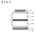
- the basic structure thereof is illustrated in Fig. 1 .
- Fig. 1 is an organic EL device comprises an electroluminescent film 103 between a first electrode 101 and a second electrode 102.
- the electroluminescent film 103 contains an organic compound capable of causing an electroluminescence.
- a bipolar carrier generation layer 104 provided as a floating electrode is embodied in the electroluminescent film 103, an insulating layer 105a(a first insulating layer) is formed between the first electrode 101 and the electroluminescent film 103.
- another insulating layer 105b(a second insulating layer) is formed between the second electrode 102 and the electroluminescent film 103.
- the bipolar carrier generation layer 104 is only provided as a single layer.
- the electroluminescent film 103 is divided into a first electroluminescent layer 103-1 and a second electroluminescent layer 103-2 through the bipolar carrier generation layer 104.
- the whole structure of the electroluminescent film 103 is sandwiched between the insulating layer 105a and the insulating layer 105b.
- the organic EL device shown in Fig. 1 has only one bipolar carrier generation layer 104. Alternatively, it may have two or more bipolar carrier generation layers.
- the organic EL device shown in Figs. 1 and 2 can be designed such that the insulating layers are thickened sufficiently to prevent carrier injections respectively from the first and second electrodes.
- the organic EL device is activated by an AC drive as the carriers are injected only from the bipolar carrier generation layer. In this case, therefore, a short circuit of the device can be prevented very effectively and the device excellent in a yield or drive stability can be offered.
- an organic electroluminescent device having a first electrode, a second electrode, and an electroluminescent film containing an organic compound capable of causing an electroluminescence and being arranged between the first electrode and the second electrode, comprises: a bipolar carrier generation layer, which is a floating electrode, is embedded in a the electroluminescent film; an insulting film between the first electrode and the electroluminescent film, which prevents a carrier injection from the first electrode to the electroluminescent film; and an insulating film between the second electrode and the electroluminescent film, which prevents a carrier injection from the second electrode to the electroluminescent film.
- an organic electroluminescent device having an electroluminescent film containing an organic compound capable of causing an electroluminescence and being arranged between a first electrode and a second electrode, comprises: a bipolar carrier generation layer, which is a floating electrode, is embodied in the electroluminescent film; an insulting film between the first electrode and the electroluminescent film; and an insulating film between the second electrode and the electroluminescent film, wherein the organic electroluminescent device is driven by an alternating current bias.
- the electroluminescent film may preferably contain a layer having bipolar property.
- the electroluminescent film includes an organic compound having electron-transporting property and an organic compound having hole-transporting property in combination with each other to form a bipolar mixed layer.
- the organic compound having bipolar property may be preferably a high molecular compound having a ⁇ -conjugated system or a ⁇ -conjugated system on the ground of simply forming a film.
- bipolar carrier generation layer from the point of transparency, it is preferable to contain an organic compound.
- organic compound for expressing a high function as a bipolar carrier generation layer, it is preferable to contain at least one of an acceptor or a donor. More preferably, both the acceptor and donor for the organic compound may be contained in the bipolar carrier generation layer.
- the bipolar carrier generation layer should have sufficient carrier. Therefore, in another aspect of the present invention, the organic electroluminescent device may comprise the bipolar carrier generation layer having an electric conductivity of 10 -10 S/m or more.
- an organic electroluminescent device (hereinafter, simply referred to as an organic EL device) one of two electrodes may be transparent so as to extract a luminescent outside from the organic EL device. Therefore, the present invention is not only limited to the configuration of the conventional device in which a transparent electrode is formed on a substrate to extract the emission of light from the substrate side through the transparent electrode, actually, but also another configuration of the device in which the emission of light is extracted from the side opposite to the substrate, or the configuration of the device in which the emission of light is extracted from the both sides of the electrode.
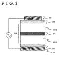
- Fig. 3 is an organic EL device of the present invention in which an AC power supply is connected to the first electrode 101 and the second electrode 102 shown in Fig. 1 .
- the same structural components as those of Fig. 1 are denoted by the same reference numerals as those of Fig. 1 .
- a luminous body having bipolar property is used as each of the first electroluminescent layer 103-1 and the second electrode electroluminescent layer 103-2.
- the potential of the first electrode is defined as V 1 and the potential of the second electrode is defined as V 2 .
- the carriers injected from the bipolar carrier generation layer are not recombined, so that they will accumulate in the boundary between the insulating layer 105a and the electroluminescent film 103 and in the boundary between the insulating layer 105b and the electroluminescent film 103 ( Fig. 4B ), respectively.
- the voltage being applied is an alternating current bias
- the voltage (V 1 ⁇ V 2 ) is applied on the device.
- the carriers are injected in the direction opposite to the case in Fig. 4A , while the carriers accumulated in Fig. 4B flow to the bipolar carrier generation layer 104 ( Fig. 4C ).
- the carriers are recombined in the first electroluminescent layer 103-1 and the second electroluminescent layer 103-2, resulting in light emission from there.
- the present organic EL device is different from the device disclosed in the above non-patent reference 5 is that the injection of carriers is only performed from the bipolar carrier generation layer being embedded in the inside but not from the outside electrode as an insulating layer 105a and an insulating layer 105b, are arranged in the device. That is, only the apparent AC flows (behavior seemingly just like intrinsic EL is shown). This can protect the short circuit of the device or the like easily and it is very useful.
- the device of the present invention does not generate leak current because of the presence of the insulating layers 105a and 105b. Therefore, it is also one of the features that improvement in efficiency is expected more.
- this invention can also be considered as a multilayer as shown in Fig. 2 .
- Fig. 5 the same reference numerals as those of Fig. 2 are used.
- the working mechanism of this example was substantially the same one as that of Fig. 3 or 4A-C , except of the follows. That is, firstly (the moment that bias was impressed at the unbias condition), carriers were already recombined to cause illumination in the second electroluminescent film 203-2 (on the other hand, in the device of Fig. 3 mentioned previously, carriers are only accumulated at the bias was firstly impressed).
- the waveform of the above described alternating current bias may be preferably sine wave, square wave, and triangle wave.
- the maximum voltage may be preferably 300 Volts or less.
- the bipolar carrier generation layer may be, for example, a metal thin film, a metal-oxide thin film, an organic conductive thin film, or a combination thereof.
- an inorganic dielectric thin film such as LiF, a metal oxide such as Li oxide, an alkali metal or an organic thin film layer including alkaline earth metal ion, or the like is provided as a cathode-side buffer layer.
- an anode-side buffer layer copper phthalocyanine may be used as an anode-side buffer layer.
- the bipolar carrier generation layer should be designed such that both carriers of holes and electrons can be injected.
- Figs. 6A-C One of examples of such a configuration is shown in Figs. 6A-C .
- a semiconductor e.g., an intrinsic semiconductor
- a redox polymer which can perform both oxidation and reduction can be considered.
- the reference numerals 601 and 611 in Figs. 6A-C denote electroluminescent layers.
- the concrete examples of the semiconductors having wide band gaps include III-group-N compounds such as GaN, AlN, BN, AlGaN, InGaN, and InAlGaN, II-VI group compounds ZnS, MgS, ZnSe, MgSe, ZnMgSSe, CdS, ZnO, and BeO, diamond, SiC, ZnGaSSe, CaF 2 , AlP, and so on.
- redox polymers include emeraldine base polyaniline (EB-PAni), and so on.
- a bipolar carrier generation layer 601 it is effective to use an organic conductive body.
- an organic conductive body there is a means for mixing a p-type organic semiconductor and an n-type organic semiconductor.
- the representative examples of the p-type organic semiconductor may include, for example, copper phthalocyanine (abbrev., CuPc) having the following structural formula (1), and other metal phthalocyanine, non-metal phthalocyanine, or the like may be applied.
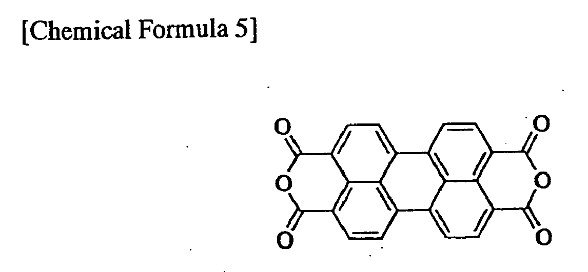
- the representative examples of the n-type organic semiconductor may include, for example, F 16 -CuPC or the like represented by the following structural formulas (2), or 3,4,9,10-perylene tetra-carboxylic acid derivatives or the like represented by the general formulas (3) (abbrev., PV), (4) (abbrev., Me-PTC), and (5) (abbrev., PTCAD).
- F 16 -CuPC or the like represented by the following structural formulas (2), or 3,4,9,10-perylene tetra-carboxylic acid derivatives or the like represented by the general formulas (3) (abbrev., PV), (4) (abbrev., Me-PTC), and (5) (abbrev., PTCAD).
- the bipolar carrier generation layer of the present invention may be formed in the shape of a thin layer or a cluster (so that carriers can be injected), there is no substantial problem.
- a representative example of the acceptor is TCNQ or a derivative thereof represented by the structural formula (6) below or a nickel complex represented by the structural formula (7) below.
- a typical example of the donor is a TTF or a derivative thereof represented by the structural formula (8).
- the organic conductor there is a technique of imparting a dark conductivity to an organic semiconductor by doping with an acceptor or a donor.
- an organic semiconductor an organic compound having a ⁇ -conjugated system, as exemplified by a conductive high polymer, may be used.
- the acceptor may be a Lewis acid such as iron(III) chloride or a halogen compound (the Lewis acid can serve as an acceptor).
- a Lewis base such as an alkali metal or an alkaline earth metal may be used (a Lewis base can serve as a donor).
- bipolar carrier generation layer from a single layer was described above. More preferably, there is another technique of constituting a bipolar carrier generation layer from two or more materials, for example, as shown in Fig. 6B and Fig. 6C .
- Fig. 6B illustrates the configuration in which a bipolar carrier generation layer 601 is constructed such that a conductive film 602 is sandwiched between electroluminescent layers 610 and 611 through an intrinsic semiconductor 603.
- the intrinsic semiconductor 603 may preferably be brought into ohmic contact with the conductive film 602.
- the conductive film 602 may be a metal, or may be various kinds of inorganic compound conductors or organic conductors described above.
- the intrinsic semiconductor 603 it may be a redox polymer or an organic conductor.
- Fig. 6C is the configuration of the bipolar carrier generation layer 601 in which the cluster-like electron injection region 605 is provided in the upper and lower sides of the conductive film 604 having a large work function.
- a carrier can be injected whichever bias.
- the conduction film 604 having a large work function ITO, Au, or the like can be considered.
- the organic conductors described above may be used.
- the clustered electron injecting region 605 may be formed by making the conventional electron injecting material into a cluster shape.
- the conventional electron injecting material may be AL:Li alloy, a metal such as Ca, an inorganic electron injecting material such as LiF, an LiF, an organic compound having a large electron affinity.
- cluster-like hole-injecting regions 605 are formed on the upper and lower sides of the conductive film 604 having a small work function.
- the conductive film 604 having a small work function may be an Al:Li alloy, Ca, or one of other organic conductors as described above.
- the cluster-like hole-injecting region 605 may be formed by making the conventional hole-injecting material into a cluster shape.
- the conventional hole-injecting material may be a metal such as Au or ITO, or an inorganic compound conductor, or an organic compound having a comparatively small ionization potential.
- the electroluminescent layer may be constructed of any structural component generally used in the organic EL device structure. However, considering the activation of the device with alternating current bias, it is preferable to form electroluminescent layer having bipolar properties.
- one comprises the steps of mixing a hole-transporting material and an electron-transporting material to form a layer having bipolar properties.
- Available hole-transporting materials include aromatic-amine compounds (i.e., having benzene-ring to nitrogen bonds) which have been widely used in the art, such as 4,4'-bis (diphenyl amino)-biphenyl (abbreviated name: TAD) and derivatives thereof, 4,4'-bis [N-(3-methylphenyl)-N-phenyl-amino]-biphenyl (abbreviated name: TPD) and 4,4'-bis [N-(1-naphthyl)-N-phenyl-amino]-biphenyl (abbreviated name: á-NPD).
- aromatic-amine compounds i.e., having benzene-ring to nitrogen bonds
- TAD 4,4'-bis [diphenyl amino)-biphenyl
- TPD 4,4'-bis [N-(
- starburst-type aromatic amine compounds such as 4,4',4"-tris (N,N-diphenyl-amino)-triphenylaminine (abbreviated name: TDATA), 4,4',4"-tris[N-(3-methylphenl)-N-phenyl-amino]-triphenylamine (abbrev., MTDATA) may be used.
- any of metal complexes have been generally used, such as metal complexes having quinoline skeletons or benzoquinoline skeletons including tris (8-quinolinolato) aluminum (abbrev., Alq), tris (4-methyl-8-quinolinolato) aluminum (abbrev., Almq), and bis (10-hydroxybenzo [h]-quinolinato) beryllium (abbrev., Bebq), and a mixed ligand complex such as bis (2-methyl-8-quinolinolato)-(4-hydroxy-biphenyl)-aluminum (abbrev., BAlq).
- metal complexes having oxazole or thiazole ligands such as zinc bis[2-(2-hydroxyphenyl)-benzoxazorato] (abbrev., Zn(BOX) 2 ), and zinc bis[2-(2-hydroxyphenyl)-benzothiazorato] (abbrev., Zn(BTZ) 2 )
- materials having electron-transporting properties include oxadiazol derivatives such as 2-(4-biphenyl)-5-(4-tert-buthylphenyl)-1,3,4-oxadiazole (abbrev., PBD) and 1,3-bis [5-(p-tert-butylphenyl)-1,3,4-oxadiazole-2-il] benzene (abbrev., OXD-7), triazole derivatives such as 3-(4-tert-butylphenyl)-4-phenyl-5-(4-biphenyl)-1,2,
- EL device materials using high molecular compounds show bipolar properties, so that they can be preferably used, specifically including polyparaphenylene polymers such as poly (2,5-dialkoxy-1,3-phenylene) (abbrev., RO-PPP), polyparaphenylene vinylene polymer such as poly (2,5-dialkoxy-1,4-phenylene vinylene) (abbrev., RO-PPV), and polyfluorene polymer such as poly(9,9-dialkylfluorene) (abbrev., PDAF).
- polyparaphenylene polymers such as poly (2,5-dialkoxy-1,3-phenylene) (abbrev., RO-PPP)
- polyparaphenylene vinylene polymer such as poly (2,5-dialkoxy-1,4-phenylene vinylene) (abbrev., RO-PPV)
- polyfluorene polymer such as poly(9,9-dialkylfluorene) (abbrev., PDAF
- any conductive material may be used.
- Aluminum, chromium, titanium, or the like may be used.
- a transparent conductive film such as ITO may be used for at least one of these electrodes for the need of transparency.
- an inorganic insulator such as aluminum oxide or calcium fluoride or an insulating organic material such as polyparaxylylene may be used. In this case, it is noted that at least the insulating layer on the light-emitting side should have transparency.
- the organic EL device of the present invention will be also applicable to white luminescence with high efficiency and long device life.
- the application not only to display but also to lighting or the like will be also considerable.
- ITO is deposited to have a thickness of 100nm as a first electrode on a glass substrate by vapor deposition, and oxide aluminum is deposited thereon to have a thickness of 300nm as an insulating layer by EB vapor deposition.
- N,N'-bis(3-methylphenyl)-N,N'-diphenyl-benzidine (abbrev., TPD) as a hole transporting material and tris (8-quinolinolato) aluminum (abbrev., Alq) as an electron transporting material are co-deposited at 1: 4 weight ratio to form a bipolar first electroluminescent layer to have a thickness of 100nm.
- DCM 4-dicyanomethylene-2-methyl-6-(p-dimethylaminostyryl)-4H-pyran
- metallic aluminum is formed to have a thickness of 30nm as a bipolar carrier generation layer.
- a second electroluminescent layer is continuously formed in exactly the same way as the first electroluminescent layer without breaking a vacuum.
- oxide aluminum is deposited to have a thickness of 300nm as an insulating layer by EB vapor deposition.
- aluminum is deposited to have a thickness of 100nm as a second electrode. Then, an organic EL device of the present invention can be formed.
- poly(vinyl phenol) is coated by spin coating to have a thickness of 200nm as an insulating layer on the glass substrate on which ITO is formed to have approximately 100nm in thick as a first electrode.
- a material for solvent is isopropanol.
- poly(2-methoxy-5-(2-ethyl-hexoxy)-1,4-phenylenevinylene) (abbrev., MEH-PPV) is dissolved in dichloroethane, and coated 80nm in thick by spin coating to form a first electroluminescent layer.
- aqueous solution of poly(ethylene dioxythiophene) doped with polystyrene sulfonic acid (abbrev., PEDOT/PSS) is spin coated to form a bipolar carrier generation layer to have a thickness of 100nm.
- a second electroluminescent layer is continuously formed in exactly the same way as the first electroluminescent layer. Further, poly(vinyl phenol) is coated by spin coating to have a thickness of 200nm as an insulating layer. Lastly, aluminum is formed to have a thickness of 100nm as a second electrode. Then, an organic EL device of the present invention can be formed.
- An organic EL device of the present invention fabricated by coating with polymer composite films containing luminous pigments and bonding without using vapor deposition will be specifically described in this embodiment.
- poly(vinyl phenol) is coated by spin coating to have a thickness of 200nm as an insulating layer on the plastic substrate (polyester substrate or polyimide substrate) on which ITO is formed 100nm in thick as a first electrode.
- a material for solvent is isopropanol.
- BND 2,5-bis(1-naphthyl)-1,3,4-oxadiazole
- PAni(CSA) 0.5 polyaniline doped with camphor-10-sulfonic acid
- PAni(CSA) 0.5 polyaniline doped with camphor-10-sulfonic acid
- HFIP 1,1,1,3,3,3-hexafluoro-2-propanol
- first electrode side substrate the substrate that is executed the deposition so far is referred to as a "first electrode side substrate".
- poly(vinyl phenol) is coated as an insulating layer to have a thickness of 200nm on a plastic substrate on which ITO having same size is formed.
- the substrate is referred to as a "second electrode side substrate".
- isopropanol solution may be spin coated as same as the previous way.
- spacer film having 650nm in thick is positioned on the periphery portion of the first electrode side substrate prepared in advance, and the second electrode side substrate is bonded to let the second electrode is inside of the substrate.
- the bonded film substrate is putted on a stainless plate of a hot plate, and weighted by superimposing another stainless plate thereon, then, heated up to 80 °C as it is.
- the film substrate is cooled with weighting, and got it out of the stainless plate, then, fitted with a lead wiring, and then, an organic EL device of the present invention is completed.
- Iso-propanol solution of poly(4-vinyl phenol) is spin coated onto an ITO glass substrate to have a thickness of 200nm.
- the film is dried at 60°C in vacuum for 30 minutes. Then, an insulating film comprising poly(4-vinyl phenol) is formed.
- dichloromethane solution in which polyvinylcarbazole (64.3mol.%) as a hole transporting material, 2.5-bis(1-naphthyl)-1,3,4-oxadiazole (BND) (35.lmol.%) as an electron transporting material, and a coumarine-6dye (0.6mol.%) as a light emission dye are dissolved is spin coated on the insulating film to have a thickness of 200nm, and dried at 60°C in vacuum for 30 minutes, then, a polymer layer is formed.
- iso-propanol suspension of ITO particles (average grain diameter 50nm) is uniformly spread by spin coating.
- dichloromethane solution in which polyvinylcarbazole (64.3mol.%) as a hole transporting material, 2.5-bis(1-naphthyl)-1,3,4-oxadiazole (BND) (35.1mol.%) as an electron transporting material, and a coumarine-6dye (0.6mol.%) as a light emission dye are dissolved is spin coated to have a thickness of 200nm, and dried at 60°C in vacuum for 1 hour, then, a polymer layer is formed.
- Iso-propanol solution of poly(4-vinyl phenol) is spin coated thereon to have a thickness of 200nm.
- the film is dried at 60°C in vacuum for 30 minutes.
- an insulating film comprising poly(4-vinyl phenol) is formed.
- an aluminium electrode is formed thereon to have a thickness of 60nm by vapor deposition.
- AC power generating sine wave is connected between the electrodes.
- AC voltage is applied to the electrode (the drive frequency range is 1kHz to 100kHz).
- the drive frequency range is 1kHz to 100kHz.
- homogeneous green luminescence of coumarin pigments exactly with the rectangular electrode shape can be observed at voltage 60V (peak voltage) viewing from the ITO electrode side.
- a measurement of luminance with a luminance meter (Topcon BM-5A) shows 30cd/m 2 at applied voltage 180V.
- the device is continuously applied 180V, since more voltage than 180V cannot applied for limitation of AC power, the device can continuously emit light with little luminance attenuation for 1 hour. Even when the drive frequency is lowered to 1kHz, luminance can be observed.
- Fig. 8 shows a relationship between voltage (illustrated with peak voltage) at drive frequency 100kHz and luminance.
- Fig. 9 shows the result of time profile of luminance strength detected using a photomultimeter measured simultaneously with applying voltage using oscilloscope. The measurement result shows that luminance is generated in synchronization with plus and minus peak voltages.
- Iso-propanol solution of poly(4-vinyl phenol) is spin coated onto an ITO glass substrate to have a thickness of 200nm.
- the film is dried at 60°C in vacuum for 30 minutes. Then, an insulating film comprising poly(4-vinyl phenol) is formed.
- dichloromethane solution in which polyvinylcarbazole (64.3mol.%) as a hole transporting material, 2.5-bis(1-naphthyl)-1,3,4-oxadiazole (BND) (35.1mol.%) as an electron transporting material, and a coumarine-6dye (0.6mol.%) as a light emission dye are dissolved is spin coated onto the insulating film to have a thickness of 200nm, and dried at 60°C in vacuum for 1 hour, then, a polymer composite film layer is formed.
- iso-propanol suspension of ITO particles (average grain diameter 50nm) is uniformly spread by spin coating.
- dichloromethane solution in which polyvinylcarbazole (64.3mol.%) as a hole transporting material, 2.5-bis(1-naphthyl)-1,3,4-oxadiazole (BND) (35.1mol.%) as an electron transporting material, and a coumarine-6dye (0.6mol.%) as a light emission dye are dissolved is spin coated thereon to have a thickness of 200nm, and dried at 60°C in vacuum for 1 hour, then, a polymer composite film layer is formed.
- BND 2.5-bis(1-naphthyl)-1,3,4-oxadiazole
- Iso-propanol solution of poly(4-vinyl phenol) is spin coated thereon to have a thickness of 200nm.
- the film is dried at 60°C in vacuum for 30 minutes.
- an insulating film comprising poly(4-vinyl phenol) is formed.
- an aluminium electrode is formed thereon to have a thickness of 60nm by vapor deposition.
- AC power generating sine wave is connected between electrodes.
- AC voltage is applied to the electrode (the drive frequency range is 1kHz to 100kHz).
- the drive frequency range is 1kHz to 100kHz.
- homogeneous green luminescence of coumarin pigments exactly with the rectangular electrode shape can be observed at voltage 70V (peak voltage) viewing from the ITO electrode side.
- a measurement of luminance with a luminance meter (Topcon BM-5A) shows 25cd/m 2 at applied voltage 180V.
- All of the elements of an organic EL device according to the present invention are fabricated by wet processing using polymer composite films containing light emitting dye and bonding without using vapor deposition.
- Iso-propanol solution of poly(4-vinyl phenol) is spin coated on a polyester substrate on which ITO is formed to have a thickness of 100nm as a bottom electrode to have a thickness of 200nm. Then, an insulating film comprising poly(4-vinyl phenol) is formed.
- dichloromethane solution in which polyvinylcarbazole (64.3mol.%) as a hole transporting material, 2.5-bis(1-naphthyl)-1,3,4-oxadiazole (BND) (35.1mol.%) as an electron transporting material, and a coumarine-6dye (0.6mol.%) as a light emission dye are dissolved is spin coated to have a thickness of 200nm, and dried at 60° in vacuum for 1 hour, then, a polymer composite film layer is formed.
- BND 2.5-bis(1-naphthyl)-1,3,4-oxadiazole
- iso-propanol suspension of ITO particles (average grain diameter 50nm) is uniformly spread by spin coating.
- a polyester substrate on which ITO is formed to have a thickness of 100nm as a bottom electrode is prepared, and iso-propanol solution of poly(4-vinyl phenol) is spin coated thereon to have a thickness of 200nm as an insulating film comprising poly(4-vinyl phenol).
- dichloromethane solution in which polyvinylcarbazole (64.3mol.%) as a hole transporting material, 2.5-bis(1-naphthyl)-1,3,4-oxadiazole (BND) (35.1mol.%) as an electron transporting material, and a coumarine-6dye (0.6mol.%) as a light emission dye are dissolved is spin coated thereon to have a thickness of 200nm, and dried at 60°C in vacuum for 1 hour, then, a polymer composite film layer is formed.
- BND 2.5-bis(1-naphthyl)-1,3,4-oxadiazole
- Two fabricated polyester substrates are bonded together to let the spin-coated materials on the substrates face each other. Then, the bonded substrate is sandwiched by two glass plates, and weighted, then, heated as it is in an oven up to 80 °C for 30 minutes.
- AC power generating sine wave is connected between two electrodes.
- AC voltage is applied to the electrode (the drive frequency range is 1kHz to 100kHz).
- the drive frequency range is 1kHz to 100kHz.
- homogeneous green luminescence of coumarin pigments exactly with the rectangular electrode shape can be observed at voltage 60V (peak voltage) viewing from the ITO electrode side.
- luminescence of same luminance can be observed from both top and bottom surfaces. Even if the substrate is bended, there is no luminance transition.
- the current efficiency can be improved and an organic EL device having good yields, high reliability, and high can be provided.
Landscapes
- Physics & Mathematics (AREA)
- Optics & Photonics (AREA)
- Engineering & Computer Science (AREA)
- Manufacturing & Machinery (AREA)
- Electroluminescent Light Sources (AREA)
Abstract
Description
- The present invention relates to an organic electroluminescent device having an organic compound layer that generates light upon application of an electric field. More particularly, the present invention relates to an organic electroluminescent device that emits light using alternating current bias.
- Compared to inorganic compounds, organic compounds have more various material systems and possibilities for synthesizing organic materials to have advanced various functions through appropriate molecular design. Further, things made from the organic compound have characteristics of being flexible, and moreover, having workability by polymerization. In light of these advantages, in recent years, the technique of photonics and electronics employing functional organic materials have been attracted attention.
- The technique of photonics utilizing optical properties of organic materials has already played an important role in contemporary industrial technology. For example, photosensitive materials such as a photoresist have become indispensable for a photolithography technique that is used for the micro machining of semiconductors. In addition, since the organic compounds themselves have properties of light absorption and light emission caused by the light absorption (fluorescence or phosphorescence), they are also well suited to light emitting materials for laser pigments or the like.
- On the other hand, since organic compounds do not have carriers themselves, they have essentially superior insulation properties. Therefore, with respect to the technique of electronics using electrical properties of organic materials, the almost organic compounds have been conventionally used as insulators such as insulating materials, protective materials, or covering materials.
- However, there is means for applying large amounts of current to the organic material that is essentially insulators. The means is increasingly coming into practical use in the electronics field. It can be broadly divided into two categories.
- One of the means, as represented by conductive polymers, is that an acceptor (electron acceptor) or a donor (electron donor) is doped to give carriers to the π-conjugate system organic compound (Reference 1: Hideki Shirakawa, Edwin J. Louis, Alan G. MacDiarmid, Chwan K. Chiang, and Alan J. Heeger, "Synthesis of Electrically Conducting Organic Polymers: Halogen Derivatives of Polyacetyrene, (CH)x", Chem. Comm., 1977, 16, 578-580). Since the carriers expand to a certain area with increased the amount of doping, the dark conductivity will also rise along with this, so that large amounts of current will become flow in the organic material.
- A part of the means for applying current to the organic material by doping an acceptor or a donor to improve the dark conductivity has already been applied in the electronics field, for example, a rechargeable secondary battery using polyaniline or polyacene, or an electric field condenser using polypyrrole.
- The other means for applying large amounts of current to the organic material is utilization of an SCLC (Space Charge Limited Current). The SCLC is the current that starts to flow by injecting and transferring a space charge from the outside. The current density of the SCLC is expressed by Child's Law, i.e.,
Formula 1 in the following. In the formula, J denotes current density, ε denotes relative permittivity, ε0 denotes permittivity of vacuum, µ denotes carrier mobility, V denotes a voltage, and d denotes a distance to which the voltage V is applied:
- Note that
Formula 1 that expresses the SCLC does not assume at all carrier-trap generated when the SCLC flows. The electric current limited by carrier-trap is referred to as TCLC (Trap Charge Limited Current) and in proportion to power of the voltage. The rate of both SCLC and TCLC are determined by bulk. Therefore the SCLC is regarded the same as TCLC hereinafter. - Here, for comparison, the current density when Ohm current flows according to Ohm's Law is shown in Formula 2. σ denotes a conductivity, and E denotes an electric field strength:

- In
Formula 2, since the conductivity σ is expressed as σ = neµ (where n denotes a carrier density, and e denotes an electric charge), the carrier density is included in the factors controlling the amount of current. Therefore, unless increase of the carrier density by doping as described above is attempted to an organic material having a certain degree of carrier mobility, the Ohm current will not flow in the organic material in which carriers hardly exist usually. - However, as shown in Formula 1, the determination factors of SCLC are the permittivity, the carrier mobility, the voltage, and the distance to which the voltage is applied. The carrier density is irrelevant. In other words, it is possible to inject a carrier from the outside and to apply the current to the organic material even an organic material is an insulator having no carriers by making the distance d sufficiently small and by using a material having significant carrier mobility µ.
- When this means is used, the amount of current in the organic material is as much as or more than that of a common semiconductor. Thus, an organic material with high carrier mobility µ, in other words, an organic material capable of transporting potentially a carrier, can be referred to as an "organic semiconductor".
- Incidentally, organic electroluminescent devices (hereinafter, organic EL devices) achieve a striking prosperity in recent years as photoelectronic devices which utilize both photonics and electrical qualities of functional organic materials among organic semiconductor devices which use the SCLC.
- The most basic structure of the organic EL device was reported by W. Tang, et al. in 1987 (Reference 2: C. W. Tang and S. A. Vanslyke, "Organic electroluminescent diodes", Applied Physics Letters, Vol. 51, No. 12, 913-915 (1987)).
- The device reported in
Reference 2 is a type of diode element in which electrodes sandwich an organic thin film to have a total thickness of approximately 100nm that is formed by laminating a hole-transporting organic compound and an electron-transporting organic compound. For the electron-transporting compound, a light emitting material (fluorescent material) is used. By applying voltage to the device, light-emission can be extracted to outside as a light emitting diode. - The light-emission mechanism is considered as follows. By applying the voltage to the organic thin film sandwiched by the electrodes, the hole and the electron injected from the electrodes are recombined inside the organic thin film, and formed to be an excited molecule (hereinafter, referred to as a "molecular exciton"), and then, light is emitted when this molecular exciton returns to its base state.
- Note that, singlet and triplet excitons formed by the organic compound can be utilized. Since the base state is normally the singlet state, the light emission from the singlet excited state is referred to as fluorescent light, and the light emission from the triplet excited state is referred to as phosphorescent light. In this specification, the light emission from either excited states will be described.
- In the above-described organic EL device, the organic thin film is normally formed into a thin film to have a thickness of about 100 to 200nm. Further, since the organic EL device is a self-luminous device in which light is generated in the organic thin film itself, a backlight that is used in a conventional liquid crystal display is not necessary. Therefore, the organic EL device has a great advantage of being able to be manufactured to be ultrathin and lightweight.
- Further, in the thin film having a thickness of about 100 to 200nm, for example, the amount of time for injecting and recombining of carriers is approximately several tens of nanoseconds taking into consideration of the carrier mobility of the organic thin film. Even if the process of carrier's recombination and light emission, light emission can be achieved within on the order of microseconds. Therefore, extremely quick response time can be included in advantages of the organic thin film.
- Because of the above-mentioned properties of thin and lightweight, the quick response time, and the like, the organic EL device is attracted an attention as a next generation flat panel display device. Further, since the organic EL display has a high level of visibility from its property of self-luminous and a broad visible range, the organic EL device is expected to be used for display screens of portable devices.
- An organic EL device is the device that utilizes means of applying SCLC to an organic semiconductor, but the SCLC intensifies the deterioration of the organic semiconductor function. As to the organic EL device, it is known that the device lifetime (half-life of the luminance) is reduced inversely proportional to the initial luminance, in other words, the amount of current flowing. (Reference 3: Yoshiharu SATO, "The Japan Society of Applied Physics/Organic Molecular Electronics and Bioelectronics", vol. 11, No. 1 (2000), 86-99).
- In view of the foregoing, above-mentioned deterioration can be reduced by improving the current efficiency (luminance generating depending on the electric current), since the necessary amount of electric current to achieve a certain luminance can be reduced. Thus, the current efficiency is an important factor for an organic device in view of the device lifetime, not to mention the power consumption.
- However, an organic EL device has a problem with respect to the current efficiency. As mentioned above, the light emission mechanism of the organic EL device is that light is converted by recombination of the injected hole and electron with each other. Therefore, in theory, it is possible to extract at most one photon from the recombination of one hole and one electron, and it is impossible to extract a plurality of photons therefrom. That is, the internal quantum efficiency (the number of emitted photons depending on injected carriers) should be at most 1.
- However, in reality, it is difficult even to bring the internal quantum efficiency close to 1. For example, in the case of the organic EL device using the fluorescent material as the luminant, the statistical generation ratio of the singlet excited state (S*) and the triplet excited state (T*) is considered to be S* : T* = 1 : 3. Therefore, the theoretical limit of the internal quantum efficiency is 0.25. (Reference 4: Tetsuo TSUTSUI, "Textbook of the 3rd seminar at Division of Organic Molecular Electronics and Bioelectronics, The Japan Society of Applied Physics" (1993), 31-37). Furthermore, as long as the fluorescent quantum yield from the fluorescent material is not φf, the internal quantum efficiency will be decreased even lower than 0.25.
- In recent years, there has been an attempt to bring the theoretical limit of the internal quantum efficiency close to 0.75 to 1 by using phosphorescent materials obtained from the light emission of the triplet excited state. The internal quantum efficiency has been actually achieved exceeding that of the fluorescent material. However, the range of material choice is unavoidably restricted since a phosphorescent material having high phosphorescent quantum efficiency φp should be used. That is caused by that the organic compounds that can release phosphorescent light at room temperature are extremely scarce.
- For this reason, as a means for improving the inferiority of the current efficiency of a device, the concept of a charge generation layer was reported in recent years (Reference 5: M. Herrmann, Junji KIDO, "49th Japan Society of Applied Physics and Related Societies" p. 1308, 27p-YL-3 (March 2002)).
- The concept of a charge generation layer is described as illustrated in
Figs.7A-B. Figs. 7A-B are frame formats of the organic EL device disclosed inReference 5 that is formed by laminating an anode, an first electroluminescent layer, a charge generation layer, a second electroluminescent layer, and a cathode. Note that the electroluminescent layer (hereinafter, an EL layer) is a layer including an organic compound that can emit light by injecting carriers. In addition, the charge generation layer does not connect to an external circuit and serves as a floating electrode. - In such an organic EL device, when voltage V is applied to the region between the anode and the cathode, electrons are injected to the first EL layer from the charge generation layer and holes are injected to the second EL layer from the charge generation layer, respectively. When seen from the external circuit, holes are moving from the anode to the cathode and electrons are moving from the cathode to the anode (
Fig. 6A ). However, it can be also seen that both holes and electrons from the charge generation layer are moving in the reverse direction (Fig. 6B ), so that carriers are recombined in both of the first EL layer and the second EL layer, and light is generated. In that case, if the current I is flowing, both of the first EL layer and the second EL layer can release photons depending on the amount of current I, respectively. Therefore, such organic EL device have the advantage of releasing two times amount of light by the same amount of current compared to an organic EL device having only one layer. (However, two times or more amount of voltage is needed compared to the organic EL device having only one layer). - In the organic EL device employing such a charge generation layer, the current efficiency can be improved significantly by laminating a number of EL layers. (However, the structure requires several times or more amount of voltage). Thus, in theory, the device lifetime can be expected to be improved along with the improvement of the current efficiency.
- However, when the current efficiency is tried to be improved using a charge generation layer, it is required that a number of EL layers should be laminated and the fabricating process become complicated. Accordingly, the partial defect possibility such as a pinhole is increased. Therefore another defects such as the dispersion of each element, the short-circuit of elements, and the like are apt to be caused. That is, the problem may be occurred with the yield of devices though the essential reliability of the device is improved according to improving the current efficiency.
- The inventor of the present invention considered in his dedicated study the means that can solve above-mentioned problems by improving the organic EL device including a charge generation layer (the inventor of the present invention refers to the charge generation layer as a bipolar carrier generation layer). The basic structure thereof is illustrated in
Fig. 1 . -
Fig. 1 is an organic EL device comprises anelectroluminescent film 103 between afirst electrode 101 and asecond electrode 102. Theelectroluminescent film 103 contains an organic compound capable of causing an electroluminescence. In the organic EL device, a bipolarcarrier generation layer 104 provided as a floating electrode is embodied in theelectroluminescent film 103, an insulatinglayer 105a(a first insulating layer) is formed between thefirst electrode 101 and theelectroluminescent film 103. In addition, another insulatinglayer 105b(a second insulating layer) is formed between thesecond electrode 102 and theelectroluminescent film 103. In the case shown inFig. 1 , the bipolarcarrier generation layer 104 is only provided as a single layer. Thus, theelectroluminescent film 103 is divided into a first electroluminescent layer 103-1 and a second electroluminescent layer 103-2 through the bipolarcarrier generation layer 104. The whole structure of theelectroluminescent film 103 is sandwiched between the insulatinglayer 105a and the insulatinglayer 105b. - By the way, the organic EL device shown in
Fig. 1 has only one bipolarcarrier generation layer 104. Alternatively, it may have two or more bipolar carrier generation layers. For instance, as shown inFig. 2 , the organic EL device may be constructed of electroluminescent layers 103-1 to 103-n and bipolar carrier generation layer 104-1 to 104-m (wherein m denotes an integer number of 1 or more, and n = m + 1), which are arranged in an alternate manner. - At this time, in the organic EL device shown in
Figs. 1 and2 can be designed such that the insulating layers are thickened sufficiently to prevent carrier injections respectively from the first and second electrodes. In this case, the organic EL device is activated by an AC drive as the carriers are injected only from the bipolar carrier generation layer. In this case, therefore, a short circuit of the device can be prevented very effectively and the device excellent in a yield or drive stability can be offered. - In a first aspect of the present invention, therefore, an organic electroluminescent device having a first electrode, a second electrode, and an electroluminescent film containing an organic compound capable of causing an electroluminescence and being arranged between the first electrode and the second electrode, comprises: a bipolar carrier generation layer, which is a floating electrode, is embedded in a the electroluminescent film; an insulting film between the first electrode and the electroluminescent film, which prevents a carrier injection from the first electrode to the electroluminescent film; and an insulating film between the second electrode and the electroluminescent film, which prevents a carrier injection from the second electrode to the electroluminescent film.
- In a second aspect of the present invention, an organic electroluminescent device having an electroluminescent film containing an organic compound capable of causing an electroluminescence and being arranged between a first electrode and a second electrode, comprises: a bipolar carrier generation layer, which is a floating electrode, is embodied in the electroluminescent film; an insulting film between the first electrode and the electroluminescent film; and an insulating film between the second electrode and the electroluminescent film, wherein the organic electroluminescent device is driven by an alternating current bias.
- Furthermore, considering that the organic electroluminescent device is driven by an alternating current bias, the electroluminescent film may preferably contain a layer having bipolar property. Alternatively, the electroluminescent film includes an organic compound having electron-transporting property and an organic compound having hole-transporting property in combination with each other to form a bipolar mixed layer. By the way, the organic compound having bipolar property may be preferably a high molecular compound having a π-conjugated system or a σ-conjugated system on the ground of simply forming a film.
- Furthermore, as a bipolar carrier generation layer, from the point of transparency, it is preferable to contain an organic compound. In this case, for expressing a high function as a bipolar carrier generation layer, it is preferable to contain at least one of an acceptor or a donor. More preferably, both the acceptor and donor for the organic compound may be contained in the bipolar carrier generation layer.
- In the organic EL device of the present invention, the bipolar carrier generation layer should have sufficient carrier. Therefore, in another aspect of the present invention, the organic electroluminescent device may comprise the bipolar carrier generation layer having an electric conductivity of 10-10 S/m or more.
-
-
Fig. 1 is a view showing a basic structure according to the present invention; -
Fig. 2 is a view showing a basic structure according to the present invention; -
Fig. 3 is a view showing an organic EL device according to the present invention; -
Figs. 4A-C are views showing working mechanismss; -
Fig. 5 is a view showing an organic EL device according to the present invention; -
Figs. 6A-C are views showing examples of structures of bipolar carrier generation layers; -
Fig. 7A and Fig. 7B are views showing organic EL device including conventional charge generation layers; -
Fig. 8 is a view showing a relationship between voltage and luminance inEmbodiment 4; and -
Fig. 9 is a view showing AC drive characteristics inEmbodiment 4. - The present invention provides in embodiments:
- (1) An organic electroluminescent device comprising:
- a first electrode;
- a second electrode; and
- an electroluminescent film containing an organic compound capable of causing an electroluminescence and being provided between the first electrode and the second electrode,
wherein a first insulating film is provided between the first electrode and the electroluminescent film, said first insulating film preventing a carrier injection from the first electrode to the electroluminescent film; and
wherein a second insulating film is provided between the second electrode and the electroluminescent film, said second insulating film preventing a carrier injection from the second electrode to the electroluminescent film. - (2) The organic electroluminescent device of (1), wherein the organic electroluminescent device is driven by an alternating current bias.
- (3) The organic electroluminescent device of (1), wherein the electroluminescent film includes a layer having bipolar property.
- (4) The organic electroluminescent device of (1), wherein the electroluminescent film includes an organic compound having electron-transporting property and an organic compound having hole-transporting property in combination with each other to form a bipolar mixed layer.
- (5) The organic electroluminescent device of (1), wherein the electroluminescent film comprises a polymer having bipolar property including a π-conjugated system or a σ-conjugated system.
- (6) The organic electroluminescent device of (1), wherein the carrier generation layer contains an organic compound.
- (7) The organic electroluminescent device of (6), wherein the carrier generation layer contains at least one of an acceptor and a donor for the organic compound.
- (8) The organic electroluminescent device of (6), wherein the carrier generation layer contains both an acceptor and a donor for the organic compound.
- (9) The organic electroluminescent device of (1), wherein the carrier generation layer has an electric conductivity of 10-10 S/m or more.
- Hereinafter, embodiments of the present invention will be described in detail while giving the working mechanism of and concrete configuration. Here, in an organic electroluminescent device (hereinafter, simply referred to as an organic EL device), one of two electrodes may be transparent so as to extract a luminescent outside from the organic EL device. Therefore, the present invention is not only limited to the configuration of the conventional device in which a transparent electrode is formed on a substrate to extract the emission of light from the substrate side through the transparent electrode, actually, but also another configuration of the device in which the emission of light is extracted from the side opposite to the substrate, or the configuration of the device in which the emission of light is extracted from the both sides of the electrode.
- At first, the working mechanism of the organic EL device of the present invention will be described with reference to
Figs. 3 and 4A-C .Fig. 3 is an organic EL device of the present invention in which an AC power supply is connected to thefirst electrode 101 and thesecond electrode 102 shown inFig. 1 . In this figure, the same structural components as those ofFig. 1 are denoted by the same reference numerals as those ofFig. 1 . In addition, a luminous body having bipolar property is used as each of the first electroluminescent layer 103-1 and the second electrode electroluminescent layer 103-2. Furthermore, the potential of the first electrode is defined as V1 and the potential of the second electrode is defined as V2. - When the device is applied with an AC voltage, at first, at the time of immediately after the application of the bias of V1 > V2, electrons move from the bipolar
carrier generation layer 104 to thefirst electrode 101, while holes move toward thesecond electrode 102. In each case, they are finally injected into the electroluminescent film 103 (Fig. 4A ). - On the other hand, as the insulating
layers electroluminescent film 103 from thefirst electrode 101 and thesecond electrode 102. Therefore, the carriers injected from the bipolar carrier generation layer are not recombined, so that they will accumulate in the boundary between the insulatinglayer 105a and theelectroluminescent film 103 and in the boundary between the insulatinglayer 105b and the electroluminescent film 103 (Fig. 4B ), respectively. - As the voltage being applied is an alternating current bias, immediately after that, the voltage (V1 < V2) is applied on the device. At this time, from the bipolar
carrier generation layer 104, the carriers are injected in the direction opposite to the case inFig. 4A , while the carriers accumulated inFig. 4B flow to the bipolar carrier generation layer 104 (Fig. 4C ). As a result, just as in the case of the organic EL device in which the conventional bipolar carrier generation layer is used (the preliminary report for the 49th Spring Meeting of the Japan Society (March, 2002), p.1308, 27p-YL-3), the carriers are recombined in the first electroluminescent layer 103-1 and the second electroluminescent layer 103-2, resulting in light emission from there. - The present organic EL device is different from the device disclosed in the above
non-patent reference 5 is that the injection of carriers is only performed from the bipolar carrier generation layer being embedded in the inside but not from the outside electrode as an insulatinglayer 105a and an insulatinglayer 105b, are arranged in the device. That is, only the apparent AC flows (behavior seemingly just like intrinsic EL is shown). This can protect the short circuit of the device or the like easily and it is very useful. - Furthermore, the device of the present invention does not generate leak current because of the presence of the insulating
layers - Furthermore, this invention can also be considered as a multilayer as shown in
Fig. 2 . The example (namely, the example in the case of m= 2 and n= 3) in which two bipolar carrier generation layers are inserted is shown inFig. 5 . InFig. 5 , the same reference numerals as those ofFig. 2 are used. In addition, the working mechanism of this example was substantially the same one as that ofFig. 3 or 4A-C , except of the follows. That is, firstly (the moment that bias was impressed at the unbias condition), carriers were already recombined to cause illumination in the second electroluminescent film 203-2 (on the other hand, in the device ofFig. 3 mentioned previously, carriers are only accumulated at the bias was firstly impressed). - Furthermore, the waveform of the above described alternating current bias may be preferably sine wave, square wave, and triangle wave. However, the present invention is not limited to these waveforms. The maximum voltage may be preferably 300 Volts or less.
- In the above description, the principle of operation of this invention was described. In the following description, we will describe the preferable configurations of the bipolar carrier generation layer to be used in the present invention and the preferable configuration of the electroluminescent film. However, the present invention is not limited to such a configuration.
- The bipolar carrier generation layer may be, for example, a metal thin film, a metal-oxide thin film, an organic conductive thin film, or a combination thereof. For instance, in the
non-patent reference 5, there is disclosed a laminate prepared by laminating a metal oxide (ITO) on an organic conductive thin film (Cs-doped BCP). In addition, on the both sides of the bipolar carrier generation layer, an inorganic dielectric thin film such as LiF, a metal oxide such as Li oxide, an alkali metal or an organic thin film layer including alkaline earth metal ion, or the like is provided as a cathode-side buffer layer. On the other hand, as an anode-side buffer layer, copper phthalocyanine may be used. - Furthermore, if it takes into consideration that the element of the present invention is driven by an alternating current bias, the bipolar carrier generation layer should be designed such that both carriers of holes and electrons can be injected. One of examples of such a configuration is shown in
Figs. 6A-C . - As shown in
Fig. 6A , when the bipolarcarrier generation layer 601 is formed from a single material, a semiconductor (e.g., an intrinsic semiconductor) having a wide band gap in which electrons are located in a conductor and holes are located in a valence band, a redox polymer which can perform both oxidation and reduction can be considered. In addition, thereference numerals Figs. 6A-C denote electroluminescent layers. - The concrete examples of the semiconductors having wide band gaps include III-group-N compounds such as GaN, AlN, BN, AlGaN, InGaN, and InAlGaN, II-VI group compounds ZnS, MgS, ZnSe, MgSe, ZnMgSSe, CdS, ZnO, and BeO, diamond, SiC, ZnGaSSe, CaF2, AlP, and so on. Furthermore, redox polymers include emeraldine base polyaniline (EB-PAni), and so on.
- Here, as a bipolar
carrier generation layer 601, it is effective to use an organic conductive body. For instance, there is a means for mixing a p-type organic semiconductor and an n-type organic semiconductor. The representative examples of the p-type organic semiconductor may include, for example, copper phthalocyanine (abbrev., CuPc) having the following structural formula (1), and other metal phthalocyanine, non-metal phthalocyanine, or the like may be applied. The representative examples of the n-type organic semiconductor may include, for example, F16-CuPC or the like represented by the following structural formulas (2), or 3,4,9,10-perylene tetra-carboxylic acid derivatives or the like represented by the general formulas (3) (abbrev., PV), (4) (abbrev., Me-PTC), and (5) (abbrev., PTCAD).


- Furthermore, there is another method using an organic conductor having conductivity by preparing a charge-transfer complex as a mixture of the acceptor (electron acceptor) of the organic compound and the donor (electron donor) of the organic compound. The charge transfer complexes tend to be crystallized and some of them show poor film formability. However, since the bipolar carrier generation layer of the present invention may be formed in the shape of a thin layer or a cluster (so that carriers can be injected), there is no substantial problem.
- A representative example of the acceptor is TCNQ or a derivative thereof represented by the structural formula (6) below or a nickel complex represented by the structural formula (7) below. In addition, a typical example of the donor is a TTF or a derivative thereof represented by the structural formula (8).


- As another example of the organic conductor, there is a technique of imparting a dark conductivity to an organic semiconductor by doping with an acceptor or a donor. As an organic semiconductor, an organic compound having a δ-conjugated system, as exemplified by a conductive high polymer, may be used. Furthermore, in addition to the examples described above, the acceptor may be a Lewis acid such as iron(III) chloride or a halogen compound (the Lewis acid can serve as an acceptor). As the donor, in addition to the examples described above, a Lewis base such as an alkali metal or an alkaline earth metal may be used (a Lewis base can serve as a donor).
- Although the example that constitutes a bipolar carrier generation layer from a single layer was described above. More preferably, there is another technique of constituting a bipolar carrier generation layer from two or more materials, for example, as shown in
Fig. 6B and Fig. 6C . -
Fig. 6B illustrates the configuration in which a bipolarcarrier generation layer 601 is constructed such that aconductive film 602 is sandwiched betweenelectroluminescent layers intrinsic semiconductor 603. In such device structure, carriers can be injected by applying either plus or minus bias thereto. Here, theintrinsic semiconductor 603 may preferably be brought into ohmic contact with theconductive film 602. Furthermore, theconductive film 602 may be a metal, or may be various kinds of inorganic compound conductors or organic conductors described above. Furthermore, instead of theintrinsic semiconductor 603, it may be a redox polymer or an organic conductor. -
Fig. 6C is the configuration of the bipolarcarrier generation layer 601 in which the cluster-likeelectron injection region 605 is provided in the upper and lower sides of theconductive film 604 having a large work function. Such a construction allows the injection of holes from theconductive film 604 and electrons from the electron-injection region, a carrier can be injected whichever bias. As theconduction film 604 having a large work function, ITO, Au, or the like can be considered. Alternatively, the organic conductors described above may be used. The clusteredelectron injecting region 605 may be formed by making the conventional electron injecting material into a cluster shape. In this case, the conventional electron injecting material may be AL:Li alloy, a metal such as Ca, an inorganic electron injecting material such as LiF, an LiF, an organic compound having a large electron affinity. - It is also possible to make the configuration of
Fig. 6C reversely from one described above. That is, cluster-like hole-injectingregions 605 are formed on the upper and lower sides of theconductive film 604 having a small work function. In this case, theconductive film 604 having a small work function may be an Al:Li alloy, Ca, or one of other organic conductors as described above. The cluster-like hole-injectingregion 605 may be formed by making the conventional hole-injecting material into a cluster shape. In this case, the conventional hole-injecting material may be a metal such as Au or ITO, or an inorganic compound conductor, or an organic compound having a comparatively small ionization potential. - Next, hereinafter, the configuration of the electroluminescent layer will be exemplified. Typically, the electroluminescent layer may be constructed of any structural component generally used in the organic EL device structure. However, considering the activation of the device with alternating current bias, it is preferable to form electroluminescent layer having bipolar properties.
- As a method for obtaining a bipolar electroluminescent layer, one comprises the steps of mixing a hole-transporting material and an electron-transporting material to form a layer having bipolar properties. Available hole-transporting materials include aromatic-amine compounds (i.e., having benzene-ring to nitrogen bonds) which have been widely used in the art, such as 4,4'-bis (diphenyl amino)-biphenyl (abbreviated name: TAD) and derivatives thereof, 4,4'-bis [N-(3-methylphenyl)-N-phenyl-amino]-biphenyl (abbreviated name: TPD) and 4,4'-bis [N-(1-naphthyl)-N-phenyl-amino]-biphenyl (abbreviated name: á-NPD). In addition, starburst-type aromatic amine compounds such as 4,4',4"-tris (N,N-diphenyl-amino)-triphenylaminine (abbreviated name: TDATA), 4,4',4"-tris[N-(3-methylphenl)-N-phenyl-amino]-triphenylamine (abbrev., MTDATA) may be used. Furthermore, as an electron-transporting material, any of metal complexes have been generally used, such as metal complexes having quinoline skeletons or benzoquinoline skeletons including tris (8-quinolinolato) aluminum (abbrev., Alq), tris (4-methyl-8-quinolinolato) aluminum (abbrev., Almq), and bis (10-hydroxybenzo [h]-quinolinato) beryllium (abbrev., Bebq), and a mixed ligand complex such as bis (2-methyl-8-quinolinolato)-(4-hydroxy-biphenyl)-aluminum (abbrev., BAlq). Furthermore, metal complexes having oxazole or thiazole ligands such as zinc bis[2-(2-hydroxyphenyl)-benzoxazorato] (abbrev., Zn(BOX)2), and zinc bis[2-(2-hydroxyphenyl)-benzothiazorato] (abbrev., Zn(BTZ)2) Furthermore, in addition to the metal complexes, materials having electron-transporting properties include oxadiazol derivatives such as 2-(4-biphenyl)-5-(4-tert-buthylphenyl)-1,3,4-oxadiazole (abbrev., PBD) and 1,3-bis [5-(p-tert-butylphenyl)-1,3,4-oxadiazole-2-il] benzene (abbrev., OXD-7), triazole derivatives such as 3-(4-tert-butylphenyl)-4-phenyl-5-(4-biphenyl)-1,2,4-triazole (abbrev., TAZ), 3-(4-tert-butylphenyl)-4-(4-ethylpheny)-5-(4-biphenylyl)-1,2,4-triazole (abbrev., p-EtTAZ), and phenanthroline derivatives such as bathophenanthroline (abbrev., BPhen) and batho-cuproine (abbrev., BCP) have an electron-transporting property.
- Furthermore, many of the EL device materials using high molecular compounds show bipolar properties, so that they can be preferably used, specifically including polyparaphenylene polymers such as poly (2,5-dialkoxy-1,3-phenylene) (abbrev., RO-PPP), polyparaphenylene vinylene polymer such as poly (2,5-dialkoxy-1,4-phenylene vinylene) (abbrev., RO-PPV), and polyfluorene polymer such as poly(9,9-dialkylfluorene) (abbrev., PDAF).
- As the first electrode and second electrode, any conductive material may be used. Aluminum, chromium, titanium, or the like may be used. Among them, preferably, a transparent conductive film such as ITO may be used for at least one of these electrodes for the need of transparency. In addition, as the insulating layer, an inorganic insulator such as aluminum oxide or calcium fluoride or an insulating organic material such as polyparaxylylene may be used. In this case, it is noted that at least the insulating layer on the light-emitting side should have transparency.
- Color mixture of each electroluminescent layer is carried out as a different luminescent color to allow white luminescence. Furthermore, therefore, the organic EL device of the present invention will be also applicable to white luminescence with high efficiency and long device life. In addition, the application not only to display but also to lighting or the like will be also considerable.
- An organic EL device of the present invention that is fabricated by the vapor deposition will be specifically described in this embodiment. First, ITO is deposited to have a thickness of 100nm as a first electrode on a glass substrate by vapor deposition, and oxide aluminum is deposited thereon to have a thickness of 300nm as an insulating layer by EB vapor deposition.
- Next, N,N'-bis(3-methylphenyl)-N,N'-diphenyl-benzidine (abbrev., TPD) as a hole transporting material and tris (8-quinolinolato) aluminum (abbrev., Alq) as an electron transporting material are co-deposited at 1: 4 weight ratio to form a bipolar first electroluminescent layer to have a thickness of 100nm. Here, 4-dicyanomethylene-2-methyl-6-(p-dimethylaminostyryl)-4H-pyran (abbrev., DCM) as a fluorescent pigment is doped to the center portion as much as 60nm (between 20 to 80nm from bottom of the thickness) to have weight ratio that TPD: Alq: DCM = 1: 4: 0.05.
- After the first electroluminescent layer is formed in such a way, metallic aluminum is formed to have a thickness of 30nm as a bipolar carrier generation layer.
- Thereafter, a second electroluminescent layer is continuously formed in exactly the same way as the first electroluminescent layer without breaking a vacuum. Moreover, oxide aluminum is deposited to have a thickness of 300nm as an insulating layer by EB vapor deposition. Lastly, aluminum is deposited to have a thickness of 100nm as a second electrode. Then, an organic EL device of the present invention can be formed.
- An organic EL device of the present invention fabricated by wet coating will be specifically described in this embodiment. First, poly(vinyl phenol) is coated by spin coating to have a thickness of 200nm as an insulating layer on the glass substrate on which ITO is formed to have approximately 100nm in thick as a first electrode. In addition, a material for solvent is isopropanol.
- Second, poly(2-methoxy-5-(2-ethyl-hexoxy)-1,4-phenylenevinylene) (abbrev., MEH-PPV) is dissolved in dichloroethane, and coated 80nm in thick by spin coating to form a first electroluminescent layer.
- After the first electroluminescent layer is formed in such a way, aqueous solution of poly(ethylene dioxythiophene) doped with polystyrene sulfonic acid (abbrev., PEDOT/PSS) is spin coated to form a bipolar carrier generation layer to have a thickness of 100nm.
- Thereafter, a second electroluminescent layer is continuously formed in exactly the same way as the first electroluminescent layer. Further, poly(vinyl phenol) is coated by spin coating to have a thickness of 200nm as an insulating layer. Lastly, aluminum is formed to have a thickness of 100nm as a second electrode. Then, an organic EL device of the present invention can be formed.
- An organic EL device of the present invention fabricated by coating with polymer composite films containing luminous pigments and bonding without using vapor deposition will be specifically described in this embodiment.
- First, poly(vinyl phenol) is coated by spin coating to have a thickness of 200nm as an insulating layer on the plastic substrate (polyester substrate or polyimide substrate) on which ITO is formed 100nm in thick as a first electrode. In addition, a material for solvent is isopropanol.
- Next, dichloromethane solution prepared from 50wt% polycarbonate as binder, 29wt% TPD as a hole transporting material,
20wt% 2,5-bis(1-naphthyl)-1,3,4-oxadiazole (abbrev., BND) as an electron transporting material, 1.0wt% coumarin 6 as a luminous pigment is spin coated on the insulating layer to form a first electroluminescent layer to have 100nm in thick. - After the first electroluminescent layer is formed in such a way, polyaniline doped with camphor-10-sulfonic acid (abbrev., PAni(CSA)0.5) is formed as a bipolar carrier generation layer to have a thickness of 50nm by spin-
coating - Then, dichloromethane solution prepared from 50wt% polycarbonate as binder, 29wt% TPD as a hole transporting material,
20wt% 2,5-bis(1-naphthyl)-1,3,4-oxadiazole (abbrev., BND) as an electron transporting material, 1.0wt% coumarin 6 as a luminous pigment is spin coated on the insulating layer to form a second electroluminescent layer to have 100nm in thick. Hereinafter, the substrate that is executed the deposition so far is referred to as a "first electrode side substrate". - In addition to above-mentioned substrate, poly(vinyl phenol) is coated as an insulating layer to have a thickness of 200nm on a plastic substrate on which ITO having same size is formed. Hereinafter, the substrate is referred to as a "second electrode side substrate". For the deposition of poly(vinyl phenol), isopropanol solution may be spin coated as same as the previous way.
- Here, spacer film having 650nm in thick is positioned on the periphery portion of the first electrode side substrate prepared in advance, and the second electrode side substrate is bonded to let the second electrode is inside of the substrate.
- The bonded film substrate is putted on a stainless plate of a hot plate, and weighted by superimposing another stainless plate thereon, then, heated up to 80 °C as it is. The film substrate is cooled with weighting, and got it out of the stainless plate, then, fitted with a lead wiring, and then, an organic EL device of the present invention is completed.
- Iso-propanol solution of poly(4-vinyl phenol) is spin coated onto an ITO glass substrate to have a thickness of 200nm. The film is dried at 60°C in vacuum for 30 minutes. Then, an insulating film comprising poly(4-vinyl phenol) is formed.
- Next, dichloromethane solution in which polyvinylcarbazole (64.3mol.%) as a hole transporting material, 2.5-bis(1-naphthyl)-1,3,4-oxadiazole (BND) (35.lmol.%) as an electron transporting material, and a coumarine-6dye (0.6mol.%) as a light emission dye are dissolved is spin coated on the insulating film to have a thickness of 200nm, and dried at 60°C in vacuum for 30 minutes, then, a polymer layer is formed.
- On top of that, iso-propanol suspension of ITO particles (average grain diameter 50nm) is uniformly spread by spin coating. Further, dichloromethane solution in which polyvinylcarbazole (64.3mol.%) as a hole transporting material, 2.5-bis(1-naphthyl)-1,3,4-oxadiazole (BND) (35.1mol.%) as an electron transporting material, and a coumarine-6dye (0.6mol.%) as a light emission dye are dissolved is spin coated to have a thickness of 200nm, and dried at 60°C in vacuum for 1 hour, then, a polymer layer is formed. Iso-propanol solution of poly(4-vinyl phenol) is spin coated thereon to have a thickness of 200nm. The film is dried at 60°C in vacuum for 30 minutes. Then, an insulating film comprising poly(4-vinyl phenol) is formed. Lastly, an aluminium electrode is formed thereon to have a thickness of 60nm by vapor deposition.
- AC power generating sine wave is connected between the electrodes. AC voltage is applied to the electrode (the drive frequency range is 1kHz to 100kHz). In the case that AC voltage is applied at drive frequency 100kHz, homogeneous green luminescence of coumarin pigments exactly with the rectangular electrode shape can be observed at voltage 60V (peak voltage) viewing from the ITO electrode side. A measurement of luminance with a luminance meter (Topcon BM-5A) shows 30cd/m2 at applied voltage 180V. When the device is continuously applied 180V, since more voltage than 180V cannot applied for limitation of AC power, the device can continuously emit light with little luminance attenuation for 1 hour. Even when the drive frequency is lowered to 1kHz, luminance can be observed.
-
Fig. 8 shows a relationship between voltage (illustrated with peak voltage) at drive frequency 100kHz and luminance.Fig. 9 shows the result of time profile of luminance strength detected using a photomultimeter measured simultaneously with applying voltage using oscilloscope. The measurement result shows that luminance is generated in synchronization with plus and minus peak voltages. - Iso-propanol solution of poly(4-vinyl phenol) is spin coated onto an ITO glass substrate to have a thickness of 200nm. The film is dried at 60°C in vacuum for 30 minutes. Then, an insulating film comprising poly(4-vinyl phenol) is formed.
- Next, dichloromethane solution in which polyvinylcarbazole (64.3mol.%) as a hole transporting material, 2.5-bis(1-naphthyl)-1,3,4-oxadiazole (BND) (35.1mol.%) as an electron transporting material, and a coumarine-6dye (0.6mol.%) as a light emission dye are dissolved is spin coated onto the insulating film to have a thickness of 200nm, and dried at 60°C in vacuum for 1 hour, then, a polymer composite film layer is formed.
- On top of that, iso-propanol suspension of ITO particles (average grain diameter 50nm) is uniformly spread by spin coating.
- Further, dichloromethane solution in which polyvinylcarbazole (64.3mol.%) as a hole transporting material, 2.5-bis(1-naphthyl)-1,3,4-oxadiazole (BND) (35.1mol.%) as an electron transporting material, and a coumarine-6dye (0.6mol.%) as a light emission dye are dissolved is spin coated thereon to have a thickness of 200nm, and dried at 60°C in vacuum for 1 hour, then, a polymer composite film layer is formed.
- Then, the steps of spin coating iso-propanol suspension of ITO particle and spin coating dichloromethane solution for forming a polymer composite film layer are respectively repeated twice.
- Iso-propanol solution of poly(4-vinyl phenol) is spin coated thereon to have a thickness of 200nm. The film is dried at 60°C in vacuum for 30 minutes. Then, an insulating film comprising poly(4-vinyl phenol) is formed. Lastly, an aluminium electrode is formed thereon to have a thickness of 60nm by vapor deposition.
- AC power generating sine wave is connected between electrodes. AC voltage is applied to the electrode (the drive frequency range is 1kHz to 100kHz). In the case that AC voltage is applied at drive frequency 100kHz, homogeneous green luminescence of coumarin pigments exactly with the rectangular electrode shape can be observed at voltage 70V (peak voltage) viewing from the ITO electrode side. A measurement of luminance with a luminance meter (Topcon BM-5A) shows 25cd/m2 at applied voltage 180V.
- All of the elements of an organic EL device according to the present invention are fabricated by wet processing using polymer composite films containing light emitting dye and bonding without using vapor deposition.
- Iso-propanol solution of poly(4-vinyl phenol) is spin coated on a polyester substrate on which ITO is formed to have a thickness of 100nm as a bottom electrode to have a thickness of 200nm. Then, an insulating film comprising poly(4-vinyl phenol) is formed.
- Next, dichloromethane solution in which polyvinylcarbazole (64.3mol.%) as a hole transporting material, 2.5-bis(1-naphthyl)-1,3,4-oxadiazole (BND) (35.1mol.%) as an electron transporting material, and a coumarine-6dye (0.6mol.%) as a light emission dye are dissolved is spin coated to have a thickness of 200nm, and dried at 60° in vacuum for 1 hour, then, a polymer composite film layer is formed.
- On top of that, iso-propanol suspension of ITO particles (average grain diameter 50nm) is uniformly spread by spin coating.
- In addition to the substrate, a polyester substrate on which ITO is formed to have a thickness of 100nm as a bottom electrode is prepared, and iso-propanol solution of poly(4-vinyl phenol) is spin coated thereon to have a thickness of 200nm as an insulating film comprising poly(4-vinyl phenol). Further, dichloromethane solution in which polyvinylcarbazole (64.3mol.%) as a hole transporting material, 2.5-bis(1-naphthyl)-1,3,4-oxadiazole (BND) (35.1mol.%) as an electron transporting material, and a coumarine-6dye (0.6mol.%) as a light emission dye are dissolved is spin coated thereon to have a thickness of 200nm, and dried at 60°C in vacuum for 1 hour, then, a polymer composite film layer is formed.
- Two fabricated polyester substrates are bonded together to let the spin-coated materials on the substrates face each other. Then, the bonded substrate is sandwiched by two glass plates, and weighted, then, heated as it is in an oven up to 80 °C for 30 minutes.
- AC power generating sine wave is connected between two electrodes. AC voltage is applied to the electrode (the drive frequency range is 1kHz to 100kHz). In the case that AC voltage is applied at drive frequency 100kHz, homogeneous green luminescence of coumarin pigments exactly with the rectangular electrode shape can be observed at voltage 60V (peak voltage) viewing from the ITO electrode side. In this case, luminescence of same luminance can be observed from both top and bottom surfaces. Even if the substrate is bended, there is no luminance transition.
- According to the present invention, the current efficiency can be improved and an organic EL device having good yields, high reliability, and high can be provided.
Claims (10)
- An organic electroluminescent device comprising:a first electrode;a second electrode; andan electroluminescent film containing an organic compound capable of causing an electroluminescence and being provided between the first electrode and the second electrode,wherein a carrier generation layer is embodied in the electroluminescent film, the carrier generation layer being a floating electrode,
wherein a first insulating film is provided between the first electrode and the electroluminescent film, the first insulating film preventing a carrier injection from the first electrode to the electroluminescent film,
wherein a second insulating film is provided between the second electrode and the electroluminescent film, the second insulating film preventing a carrier injection from the second electrode to the electroluminescent film, and
wherein the carrier generation layer is formed from a single material. - An organic electroluminescent device comprising:a first electrode;a second electrode; andan electroluminescent film containing an organic compound capable of causing an electroluminescence and being provided between the first electrode and the second electrode,wherein a carrier generation layer is embodied in the electroluminescent film, the carrier generation layer being a floating electrode,
wherein a first insulating film is provided between the first electrode and the electroluminescent film, the first insulating film preventing a carrier injection from the first electrode to the electroluminescent film,
wherein a second insulating film is provided between the second electrode and the electroluminescent film, the second insulating film preventing a carrier injection from the second electrode to the electroluminescent film, and
wherein the carrier generation layer comprises a first electroluminescent layer, a second electroluminescent layer, and an intrinsic semiconductor, and the intrinsic semiconductor is interposed between the first and second electroluminescent layers. - An organic electroluminescent device comprising:a first electrode;a second electrode; andan electroluminescent film containing an organic compound capable of causing an electroluminescence and being provided between the first electrode and the second electrode,wherein a carrier generation layer is embodied in the electroluminescent film, the carrier generation layer being a floating electrode,
wherein a first insulating film is provided between the first electrode and the electroluminescent film, the first insulating film preventing a carrier injection from the first electrode to the electroluminescent film,
wherein a second insulating film is provided between the second electrode and the electroluminescent film, the second insulating film preventing a carrier injection from the second electrode to the electroluminescent film, and
wherein the carrier generation layer comprises a conductive film, a first electron injection region on the conductive film, a second electron injection region under the conductive film,
wherein the conductive film is in contact with the first and second electron injection regions. - An organic electroluminescent device according to any one of claims 1 to 3,
wherein the electroluminescent film comprises a layer having bipolar property. - An organic electroluminescent device according to any one of claims 1 to 3,
wherein the organic electroluminescent device is configured to be driven by an alternating current bias. - An organic electroluminescent device according to any one of claims 1 to 3,
wherein the carrier generation layer has an electric conductivity of 10-10 S/m or more. - An organic electroluminescent device according to any one of claims 1 to 3,
wherein a drive frequency of the organic electroluminescent device is in a range of 1 to 100 KHz. - An organic electroluminescent device according to any one of claims 1 to 3,
wherein a waveform of the alternating current bias is selected from a sine wave, a square wave, and a triangle wave. - An organic electroluminescent device according to any one of claims 1 to 3,
wherein the first and second electroluminescent layers are cluster-like. - An organic electroluminescent device according to claim 3,
wherein parts of top and upper surfaces of the conductive film are in contact with the electroluminescent film.
Applications Claiming Priority (2)
| Application Number | Priority Date | Filing Date | Title |
|---|---|---|---|
| JP2002233526 | 2002-08-09 | ||
| EP03016830A EP1388904B1 (en) | 2002-08-09 | 2003-07-23 | Organic electroluminescent device |
Related Parent Applications (2)
| Application Number | Title | Priority Date | Filing Date |
|---|---|---|---|
| EP03016830A Division EP1388904B1 (en) | 2002-08-09 | 2003-07-23 | Organic electroluminescent device |
| EP03016830.6 Division | 2003-07-23 |
Publications (3)
| Publication Number | Publication Date |
|---|---|
| EP2065950A2 true EP2065950A2 (en) | 2009-06-03 |
| EP2065950A3 EP2065950A3 (en) | 2009-06-24 |
| EP2065950B1 EP2065950B1 (en) | 2012-06-27 |
Family
ID=30437801
Family Applications (2)
| Application Number | Title | Priority Date | Filing Date |
|---|---|---|---|
| EP03016830A Expired - Lifetime EP1388904B1 (en) | 2002-08-09 | 2003-07-23 | Organic electroluminescent device |
| EP09003786A Expired - Lifetime EP2065950B1 (en) | 2002-08-09 | 2003-07-23 | Organic electroluminescent device |
Family Applications Before (1)
| Application Number | Title | Priority Date | Filing Date |
|---|---|---|---|
| EP03016830A Expired - Lifetime EP1388904B1 (en) | 2002-08-09 | 2003-07-23 | Organic electroluminescent device |
Country Status (6)
| Country | Link |
|---|---|
| US (5) | US7291969B2 (en) |
| EP (2) | EP1388904B1 (en) |
| KR (2) | KR101065597B1 (en) |
| CN (2) | CN100459207C (en) |
| DE (1) | DE60327024D1 (en) |
| TW (1) | TWI272874B (en) |
Cited By (8)
| Publication number | Priority date | Publication date | Assignee | Title |
|---|---|---|---|---|
| US7964891B2 (en) | 2004-08-04 | 2011-06-21 | Semiconductor Energy Laboratory Co., Ltd. | Light-emitting element, display device, and electronic appliance |
| US8018152B2 (en) | 2004-05-20 | 2011-09-13 | Semiconductor Energy Laboratory Co., Ltd. | Light-emitting element including intermediate conductive layer having a hole-injection layer with an island-like structure |
| US8076676B2 (en) | 2006-06-01 | 2011-12-13 | Semiconductor Energy Laboratory Co., Ltd. | Light-emitting element, light-emitting device and an electronic device which include two layers including the same light-emitting organic compound |
| CN104600095A (en) * | 2014-12-31 | 2015-05-06 | 北京维信诺科技有限公司 | Display device |
| US9368744B2 (en) | 2010-04-01 | 2016-06-14 | Samsung Display Co., Ltd. | Organic light emitting diode device including multiple hole injection layers |
| US9397308B2 (en) | 2006-12-04 | 2016-07-19 | Semiconductor Energy Laboratory Co., Ltd. | Light emitting element, light emitting device, and electronic device |
| US9876151B2 (en) | 2010-09-14 | 2018-01-23 | Semiconductor Energy Laboratory Co., Ltd. | Solid-state light-emitting element, light-emitting device, and lighting device |
| US10573829B2 (en) | 2011-02-16 | 2020-02-25 | Semiconductor Energy Laboratory Co., Ltd. | Light-emitting element |
Families Citing this family (111)
| Publication number | Priority date | Publication date | Assignee | Title |
|---|---|---|---|---|
| US7956349B2 (en) | 2001-12-05 | 2011-06-07 | Semiconductor Energy Laboratory Co., Ltd. | Organic semiconductor element |
| US6815723B2 (en) * | 2001-12-28 | 2004-11-09 | Semiconductor Energy Laboratory Co., Ltd. | Light emitting device, method of manufacturing the same, and manufacturing apparatus therefor |
| US7098069B2 (en) * | 2002-01-24 | 2006-08-29 | Semiconductor Energy Laboratory Co., Ltd. | Light emitting device, method of preparing the same and device for fabricating the same |
| JP2003303683A (en) * | 2002-04-09 | 2003-10-24 | Semiconductor Energy Lab Co Ltd | Luminous device |
| EP1367659B1 (en) | 2002-05-21 | 2012-09-05 | Semiconductor Energy Laboratory Co., Ltd. | Organic field effect transistor |
| US7045955B2 (en) * | 2002-08-09 | 2006-05-16 | Semiconductor Energy Laboratory Co., Ltd. | Electroluminescence element and a light emitting device using the same |
| EP1388903B1 (en) * | 2002-08-09 | 2016-03-16 | Semiconductor Energy Laboratory Co., Ltd. | Organic electroluminescent device |
| TWI272874B (en) | 2002-08-09 | 2007-02-01 | Semiconductor Energy Lab | Organic electroluminescent device |
| US7158161B2 (en) * | 2002-09-20 | 2007-01-02 | Matsushita Electric Industrial Co., Ltd. | Organic electroluminescence element and an exposure unit and image-forming apparatus both using the element |
| WO2004060026A1 (en) | 2002-12-26 | 2004-07-15 | Semiconductor Energy Laboratory Co., Ltd. | Organic light emitting element |
| CN1742518B (en) * | 2003-01-29 | 2010-09-29 | 株式会社半导体能源研究所 | light emitting device |
| US7333072B2 (en) * | 2003-03-24 | 2008-02-19 | Semiconductor Energy Laboratory Co., Ltd. | Thin film integrated circuit device |
| JP2006526274A (en) * | 2003-04-23 | 2006-11-16 | ツェン−ホン ルー | Light emitting device with embedded charge injection electrode |
| ATE532386T1 (en) * | 2003-07-02 | 2011-11-15 | Idemitsu Kosan Co | ORGANIC ELECTROLUMINENCE COMPONENT AND DISPLAY THEREOF |
| US7504049B2 (en) * | 2003-08-25 | 2009-03-17 | Semiconductor Energy Laboratory Co., Ltd. | Electrode device for organic device, electronic device having electrode device for organic device, and method of forming electrode device for organic device |
| US7511421B2 (en) | 2003-08-25 | 2009-03-31 | Semiconductor Energy Laboratory Co., Ltd. | Mixed metal and organic electrode for organic device |
| KR101246247B1 (en) * | 2003-08-29 | 2013-03-21 | 가부시키가이샤 한도오따이 에네루기 켄큐쇼 | Electroluminescent device and light-emitting device including the same |
| JP5167571B2 (en) | 2004-02-18 | 2013-03-21 | ソニー株式会社 | Display element |
| JP4175273B2 (en) | 2004-03-03 | 2008-11-05 | セイコーエプソン株式会社 | Method for manufacturing stacked organic electroluminescence element and display device |
| KR100853991B1 (en) * | 2004-03-26 | 2008-08-25 | 간사이 덴료쿠 가부시키가이샤 | Bipolar semiconductor device and manufacturing method thereof |
| CN101673807B (en) * | 2004-04-28 | 2012-07-18 | 株式会社半导体能源研究所 | Light-emitting element and method of manufacturing the same, and light-emitting device using the light-emitting element |
| CN1965613B (en) | 2004-05-21 | 2010-06-16 | 株式会社半导体能源研究所 | Light-emitting element and light-emitting device using the same |
| KR101152935B1 (en) * | 2004-05-21 | 2012-06-08 | 가부시키가이샤 한도오따이 에네루기 켄큐쇼 | Light emitting element and light emitting device |
| JP4461367B2 (en) * | 2004-05-24 | 2010-05-12 | ソニー株式会社 | Display element |
| US7733441B2 (en) * | 2004-06-03 | 2010-06-08 | Semiconductor Energy Labortory Co., Ltd. | Organic electroluminescent lighting system provided with an insulating layer containing fluorescent material |
| US20060181197A1 (en) * | 2004-07-01 | 2006-08-17 | Kumio Nago | Electroluminescent device and display |
| CN1738069A (en) * | 2004-08-17 | 2006-02-22 | 国际商业机器公司 | Electronic device manufacturing method and electronic device whose electrodes have enhanced injection characteristics |
| CN101032040B (en) * | 2004-09-30 | 2012-05-30 | 株式会社半导体能源研究所 | Light emitting element and light emitting device |
| US7719496B2 (en) * | 2004-11-23 | 2010-05-18 | Samsung Mobile Display Co., Ltd. | Organic thin film transistor, method of manufacturing the same, and flat panel display device with the organic thin film transistor |
| JP2006164708A (en) | 2004-12-06 | 2006-06-22 | Semiconductor Energy Lab Co Ltd | Electronic equipment and light emitting device |
| JP4496948B2 (en) * | 2004-12-13 | 2010-07-07 | 株式会社豊田自動織機 | Organic EL device |
| JP4496949B2 (en) | 2004-12-13 | 2010-07-07 | 株式会社豊田自動織機 | Organic EL device |
| US7307278B2 (en) * | 2004-12-22 | 2007-12-11 | General Electric Company | Organic electronic devices having two dimensional series interconnections |
| US8026531B2 (en) | 2005-03-22 | 2011-09-27 | Semiconductor Energy Laboratory Co., Ltd. | Light emitting device |
| US20060244373A1 (en) * | 2005-04-28 | 2006-11-02 | Semiconductor Energy Laboratory Co., Ltd. | Light emitting device and method for manufacturing thereof |
| US8487527B2 (en) * | 2005-05-04 | 2013-07-16 | Lg Display Co., Ltd. | Organic light emitting devices |
| US7777407B2 (en) * | 2005-05-04 | 2010-08-17 | Lg Display Co., Ltd. | Organic light emitting devices comprising a doped triazine electron transport layer |
| US7795806B2 (en) * | 2005-05-20 | 2010-09-14 | Lg Display Co., Ltd. | Reduced reflectance display devices containing a thin-layer metal-organic mixed layer (MOML) |
| US7728517B2 (en) * | 2005-05-20 | 2010-06-01 | Lg Display Co., Ltd. | Intermediate electrodes for stacked OLEDs |
| US7811679B2 (en) * | 2005-05-20 | 2010-10-12 | Lg Display Co., Ltd. | Display devices with light absorbing metal nanoparticle layers |
| US7750561B2 (en) * | 2005-05-20 | 2010-07-06 | Lg Display Co., Ltd. | Stacked OLED structure |
| US7943244B2 (en) * | 2005-05-20 | 2011-05-17 | Lg Display Co., Ltd. | Display device with metal-organic mixed layer anodes |
| JP4435033B2 (en) * | 2005-06-16 | 2010-03-17 | 株式会社東芝 | Fluorescent pattern formed article, recording medium, security medium, and recording method |
| WO2007004729A1 (en) | 2005-07-06 | 2007-01-11 | Semiconductor Energy Laboratory Co., Ltd. | Light-emitting element, light-emitting device, and electronic device |
| US7327081B2 (en) * | 2005-08-31 | 2008-02-05 | Chunghwa Picture Tubes, Ltd. | Stacked organic electroluminescent device and method for manufacturing thereof |
| EP1784055A3 (en) * | 2005-10-17 | 2009-08-05 | Semiconductor Energy Laboratory Co., Ltd. | Lighting system |
| JP2007194194A (en) * | 2005-12-22 | 2007-08-02 | Matsushita Electric Ind Co Ltd | ELECTROLUMINESCENCE ELEMENT AND DISPLAY DEVICE, EXPOSURE DEVICE, AND ILLUMINATION DEVICE USING THE SAME |
| US8698392B2 (en) * | 2006-02-07 | 2014-04-15 | Sumitomo Chemical Company, Limited | Organic electroluminescent element |
| US7528418B2 (en) * | 2006-02-24 | 2009-05-05 | Semiconductor Energy Laboratory Co., Ltd. | Light-emitting device |
| WO2007132965A1 (en) * | 2006-05-12 | 2007-11-22 | Cheong-A Baek | High brightness electro luminescence device and method for manufacturing thereof |
| JPWO2007139033A1 (en) * | 2006-05-26 | 2009-10-08 | 富士フイルム株式会社 | Surface-emitting electroluminescent device |
| EP2064746A2 (en) | 2006-09-29 | 2009-06-03 | University of Florida Research Foundation, Incorporated | Method and apparatus for infrared detection and display |
| KR100873535B1 (en) * | 2006-12-20 | 2008-12-11 | 삼성에스디아이 주식회사 | Backlight unit using electron-emitting device and liquid crystal display device using same |
| CN101636856A (en) * | 2007-03-22 | 2010-01-27 | 日本先锋公司 | Organic electroluminescent device, display device including the same, and power generation device |
| JP4939284B2 (en) * | 2007-04-05 | 2012-05-23 | 財団法人山形県産業技術振興機構 | Organic electroluminescent device |
| KR100882911B1 (en) * | 2007-08-16 | 2009-02-10 | 삼성모바일디스플레이주식회사 | Organic electroluminescent device and manufacturing method thereof |
| DE102007058005B4 (en) * | 2007-09-25 | 2018-05-17 | Osram Oled Gmbh | Radiation-emitting device and method for its production |
| DE102008045029B4 (en) * | 2007-09-28 | 2016-12-22 | Osram Oled Gmbh | Radiation-emitting component and operating method and operating arrangement |
| EP2068380B1 (en) * | 2007-10-15 | 2011-08-17 | Novaled AG | Organic electroluminescent component |
| DE102008046857B4 (en) | 2007-12-17 | 2025-03-27 | Pictiva Displays International Limited | OLED for AC operation and manufacturing processes |
| US7755156B2 (en) * | 2007-12-18 | 2010-07-13 | Palo Alto Research Center Incorporated | Producing layered structures with lamination |
| US7586080B2 (en) * | 2007-12-19 | 2009-09-08 | Palo Alto Research Center Incorporated | Producing layered structures with layers that transport charge carriers in which each of a set of channel regions or portions operates as an acceptable switch |
| US8283655B2 (en) | 2007-12-20 | 2012-10-09 | Palo Alto Research Center Incorporated | Producing layered structures with semiconductive regions or subregions |
| WO2009142030A1 (en) * | 2008-05-19 | 2009-11-26 | シャープ株式会社 | Organic electroluminescent device, display device and illuminating device |
| DE102008025755A1 (en) * | 2008-05-29 | 2009-12-03 | Osram Opto Semiconductors Gmbh | Organic light-emitting component and light-emitting means with such a component |
| DE102009016957A1 (en) | 2009-04-14 | 2010-12-16 | Technische Universität Dresden | Organic electroluminescent device |
| JP5624140B2 (en) * | 2009-09-01 | 2014-11-12 | コーニンクレッカ フィリップス エヌ ヴェ | Lighting device including power supply |
| KR101351410B1 (en) * | 2009-09-29 | 2014-01-14 | 엘지디스플레이 주식회사 | White Organic Light Emitting Device |
| JPWO2011046166A1 (en) * | 2009-10-14 | 2013-03-07 | コニカミノルタホールディングス株式会社 | ORGANIC ELECTROLUMINESCENCE ELEMENT AND LIGHTING DEVICE USING THE SAME |
| CA2781432A1 (en) * | 2009-11-24 | 2011-06-03 | University Of Florida Research Foundation, Inc. | Method and apparatus for sensing infrared radiation |
| KR20120100709A (en) * | 2010-01-15 | 2012-09-12 | 이데미쓰 고산 가부시키가이샤 | Organic electroluminescent element |
| JP2012009420A (en) | 2010-05-21 | 2012-01-12 | Semiconductor Energy Lab Co Ltd | Light emitting device and illumination device |
| JP5778261B2 (en) | 2010-05-24 | 2015-09-16 | ユニバーシティ オブ フロリダ リサーチ ファウンデーション,インク.University Of Florida Reseatch Foundation,Inc. | Method and apparatus for providing a charge blocking layer on an infrared upconversion device |
| WO2012014759A1 (en) | 2010-07-26 | 2012-02-02 | Semiconductor Energy Laboratory Co., Ltd. | Light-emitting device, lighting device, and manufacturing method of light-emitting device |
| US8994011B2 (en) * | 2010-08-17 | 2015-03-31 | Lg Chem, Ltd. | Organic light-emitting device |
| CN102074658B (en) * | 2010-11-01 | 2014-08-27 | 中国科学院长春应用化学研究所 | Electric charge production layer, lamination layer organic light-emitting diode and preparation method thereof |
| JP5707107B2 (en) * | 2010-11-22 | 2015-04-22 | 浜松ホトニクス株式会社 | Spectroscopic sensor |
| JP5970198B2 (en) | 2011-02-14 | 2016-08-17 | 株式会社半導体エネルギー研究所 | Lighting device |
| US8764504B2 (en) | 2011-02-25 | 2014-07-01 | Semiconductor Energy Laboratory Co., Ltd. | Lighting device and method for manufacturing the same |
| KR101917752B1 (en) | 2011-05-11 | 2018-11-13 | 가부시키가이샤 한도오따이 에네루기 켄큐쇼 | Light-emitting element, light-emitting module, light-emmiting panel, and light-emitting device |
| CN102842680A (en) * | 2011-06-21 | 2012-12-26 | 海洋王照明科技股份有限公司 | Organic electroluminescent device and preparation method thereof |
| RU2014102650A (en) | 2011-06-30 | 2015-08-10 | Юниверсити Оф Флорида Рисеч Фаундэйшн, Инк. | REINFORCING INFRARED PHOTODETECTOR AND ITS APPLICATION FOR DETECTING IR RADIATION |
| WO2013008765A1 (en) | 2011-07-08 | 2013-01-17 | Semiconductor Energy Laboratory Co., Ltd. | Light-emitting module, light-emitting device, and method for manufacturing the light-emitting module |
| TW201338232A (en) * | 2012-03-02 | 2013-09-16 | Innocom Tech Shenzhen Co Ltd | Series organic electroluminescent module |
| KR101512218B1 (en) * | 2012-05-25 | 2015-04-14 | 주식회사 엘지화학 | Organic light emitting device |
| KR101657057B1 (en) * | 2012-05-31 | 2016-09-13 | 엘지디스플레이 주식회사 | Organoluminescent device |
| CN102841281B (en) * | 2012-09-18 | 2015-07-22 | 苏州纳方科技发展有限公司 | Detection method and device for LED epitaxial wafer |
| CN103972419A (en) * | 2013-01-31 | 2014-08-06 | 海洋王照明科技股份有限公司 | Organic light-emitting device and production method thereof |
| CN104037327A (en) * | 2013-03-06 | 2014-09-10 | 海洋王照明科技股份有限公司 | Stacked organic light emitting device and preparation method |
| CN104183745A (en) * | 2013-05-21 | 2014-12-03 | 海洋王照明科技股份有限公司 | Organic light emission device and manufacturing method thereof |
| US9433040B2 (en) | 2013-06-14 | 2016-08-30 | Micron Technology, Inc. | Light-emitting metal-oxide-semiconductor devices and associated systems, devices, and methods |
| KR102126533B1 (en) * | 2013-10-04 | 2020-06-24 | 엘지디스플레이 주식회사 | Organic emitting device and organic emitting display device comprising the same |
| GB2533112B (en) * | 2014-12-09 | 2017-04-05 | Dst Innovations Ltd | Electroluminescent elements and methods of construction |
| US9991471B2 (en) | 2014-12-26 | 2018-06-05 | Semiconductor Energy Laboratory Co., Ltd. | Light-emitting element, light-emitting device, display device, and electronic device |
| CN104617232B (en) * | 2015-01-05 | 2017-04-19 | 信利(惠州)智能显示有限公司 | Organic Light-Emitting Diodes (OLED) manufacturing method and OLED |
| JP6548725B2 (en) * | 2015-05-11 | 2019-07-24 | 日本放送協会 | ORGANIC THIN FILM AND METHOD FOR MANUFACTURING ORGANIC THIN FILM, ORGANIC ELECTROLUMINESCENT DEVICE, DISPLAY DEVICE, LIGHTING DEVICE, ORGANIC THIN FILM SOLAR CELL, THIN FILM TRANSISTOR, AND COATING COMPOSITION |
| EP3299942A4 (en) * | 2015-05-20 | 2018-05-23 | Konica Minolta, Inc. | Organic electroluminescent module, smart device, and illumination apparatus |
| CA2988784A1 (en) | 2015-06-11 | 2017-03-09 | University Of Florida Research Foundation, Incorporated | Monodisperse, ir-absorbing nanoparticles and related methods and devices |
| CN105163412B (en) * | 2015-06-19 | 2018-06-15 | 北京大学深圳研究生院 | Planar electroluminescent device and application thereof |
| CN104966789A (en) * | 2015-06-30 | 2015-10-07 | 深圳市华星光电技术有限公司 | Charge coupling layer, manufacturing method thereof and stacked OLED device |
| JP6549434B2 (en) * | 2015-07-15 | 2019-07-24 | コニカミノルタ株式会社 | Method of manufacturing organic electroluminescent device |
| CN105161629B (en) * | 2015-08-18 | 2018-07-03 | Tcl集团股份有限公司 | Exchange driving QLED and preparation method thereof |
| CN105609650A (en) * | 2015-12-27 | 2016-05-25 | 复旦大学 | Charge generation layer based organic light-emitting device driven by alternating current voltage |
| KR101858414B1 (en) * | 2017-11-30 | 2018-05-16 | 씨큐브 주식회사 | Pearlescent pigment containing organic or inorganic fluorescent substance for security applications |
| CN109065746B (en) * | 2018-07-17 | 2020-01-14 | 华南理工大学 | Organic light emitting diode capable of emitting light in forward and reverse directions |
| KR102177586B1 (en) * | 2018-11-26 | 2020-11-11 | 엘티소재주식회사 | Heterocyclic compound and organic light emitting device comprising the same |
| CN109686851A (en) * | 2018-12-26 | 2019-04-26 | 上海晶合光电科技有限公司 | A kind of Organic Light Emitting Diode and preparation method thereof |
| CN110148593B (en) * | 2019-05-08 | 2020-09-08 | 深圳市华星光电半导体显示技术有限公司 | Organic electroluminescent device |
| CN111106263A (en) * | 2019-12-06 | 2020-05-05 | 北京大学深圳研究生院 | Planar organic electroluminescent device with color regulated by full-period light-emitting alternating current |
| CN112151690B (en) * | 2020-09-28 | 2024-04-09 | 京东方科技集团股份有限公司 | Organic light emitting diode and manufacturing method thereof, display panel and display device |
| WO2025199753A1 (en) * | 2024-03-26 | 2025-10-02 | 京东方科技集团股份有限公司 | Light-emitting device and display panel |
Family Cites Families (88)
| Publication number | Priority date | Publication date | Assignee | Title |
|---|---|---|---|---|
| JPS55140277A (en) | 1979-04-19 | 1980-11-01 | Ricoh Co Ltd | Organic phtotovoltaic element |
| JPS6028278A (en) | 1983-07-26 | 1985-02-13 | Mitsubishi Electric Corp | Photoelectric conversion element |
| US4878097A (en) * | 1984-05-15 | 1989-10-31 | Eastman Kodak Company | Semiconductor photoelectric conversion device and method for making same |
| US4950614A (en) * | 1984-05-15 | 1990-08-21 | Semiconductor Energy Laboratory Co., Ltd. | Method of making a tandem type semiconductor photoelectric conversion device |
| US4741976A (en) * | 1984-07-31 | 1988-05-03 | Canon Kabushiki Kaisha | Electroluminescent device |
| US4871236A (en) * | 1985-09-18 | 1989-10-03 | Kabushiki Kaisha Toshiba | Organic thin film display element |
| JP2813428B2 (en) | 1989-08-17 | 1998-10-22 | 三菱電機株式会社 | Field effect transistor and liquid crystal display device using the field effect transistor |
| JPH04192376A (en) | 1990-11-22 | 1992-07-10 | Sekisui Chem Co Ltd | Tandem organic solar battery |
| US5093698A (en) | 1991-02-12 | 1992-03-03 | Kabushiki Kaisha Toshiba | Organic electroluminescent device |
| US5229310A (en) | 1991-05-03 | 1993-07-20 | Motorola, Inc. | Method for making a self-aligned vertical thin-film transistor in a semiconductor device |
| US5294870A (en) | 1991-12-30 | 1994-03-15 | Eastman Kodak Company | Organic electroluminescent multicolor image display device |
| JP2605555B2 (en) * | 1992-09-14 | 1997-04-30 | 富士ゼロックス株式会社 | Inorganic thin film EL device |
| JP3300065B2 (en) | 1992-11-13 | 2002-07-08 | パイオニア株式会社 | Organic electroluminescence device |
| JPH06260286A (en) | 1993-03-08 | 1994-09-16 | Olympus Optical Co Ltd | Thin film electroluminescence element |
| JPH06318725A (en) | 1993-05-10 | 1994-11-15 | Ricoh Co Ltd | Photovoltaic element and its manufacture |
| GB9317932D0 (en) | 1993-08-26 | 1993-10-13 | Cambridge Display Tech Ltd | Electroluminescent devices |
| US5682043A (en) * | 1994-06-28 | 1997-10-28 | Uniax Corporation | Electrochemical light-emitting devices |
| US5552678A (en) * | 1994-09-23 | 1996-09-03 | Eastman Kodak Company | AC drive scheme for organic led |
| KR0164457B1 (en) * | 1995-01-20 | 1999-04-15 | 김은영 | Manufacturing method and white lighting el element |
| US5858561A (en) * | 1995-03-02 | 1999-01-12 | The Ohio State University | Bipolar electroluminescent device |
| JP3561549B2 (en) | 1995-04-07 | 2004-09-02 | 三洋電機株式会社 | Organic electroluminescence device |
| US5677546A (en) * | 1995-05-19 | 1997-10-14 | Uniax Corporation | Polymer light-emitting electrochemical cells in surface cell configuration |
| JP4477150B2 (en) | 1996-01-17 | 2010-06-09 | 三星モバイルディスプレイ株式會社 | Organic thin film EL device |
| JP3808534B2 (en) * | 1996-02-09 | 2006-08-16 | Tdk株式会社 | Image display device |
| US6255774B1 (en) | 1996-09-04 | 2001-07-03 | Cambridge Display Technology, Ltd. | Multilayer cathode for organic light-emitting device |
| JP3173395B2 (en) | 1996-11-26 | 2001-06-04 | 富士ゼロックス株式会社 | Charge transporting material and method for producing charge transporting fine particles used therefor |
| EP0880305A4 (en) | 1996-11-27 | 2000-07-05 | Tdk Corp | Organic el element |
| JPH10270171A (en) | 1997-01-27 | 1998-10-09 | Junji Kido | Organic electroluminescent device |
| US5917280A (en) * | 1997-02-03 | 1999-06-29 | The Trustees Of Princeton University | Stacked organic light emitting devices |
| TW418590B (en) * | 1997-04-25 | 2001-01-11 | Tdk Corp | Organic electroluminescent device |
| KR100248392B1 (en) * | 1997-05-15 | 2000-09-01 | 정선종 | Organic Active Driving Electroluminescent Device Combined with Organic Field Effect Transistor and Fabrication Method |
| US6337492B1 (en) | 1997-07-11 | 2002-01-08 | Emagin Corporation | Serially-connected organic light emitting diode stack having conductors sandwiching each light emitting layer |
| AU8991598A (en) * | 1997-09-05 | 1999-03-29 | Cambridge Display Technology Limited | Self-assembled transport layers for oleds |
| JPH11162646A (en) | 1997-11-26 | 1999-06-18 | Chisso Corp | Organic electroluminescent element |
| US6300612B1 (en) * | 1998-02-02 | 2001-10-09 | Uniax Corporation | Image sensors made from organic semiconductors |
| JPH11251067A (en) | 1998-03-02 | 1999-09-17 | Junji Kido | Organic electroluminescent device |
| GB9806066D0 (en) | 1998-03-20 | 1998-05-20 | Cambridge Display Tech Ltd | Multilayer photovoltaic or photoconductive devices |
| JP3875401B2 (en) * | 1998-05-12 | 2007-01-31 | Tdk株式会社 | Organic EL display device and organic EL element |
| JP3884564B2 (en) | 1998-05-20 | 2007-02-21 | 出光興産株式会社 | Organic EL light emitting device and light emitting device using the same |
| US6198092B1 (en) * | 1998-08-19 | 2001-03-06 | The Trustees Of Princeton University | Stacked organic photosensitive optoelectronic devices with an electrically parallel configuration |
| US6297495B1 (en) * | 1998-08-19 | 2001-10-02 | The Trustees Of Princeton University | Organic photosensitive optoelectronic devices with a top transparent electrode |
| US6451415B1 (en) * | 1998-08-19 | 2002-09-17 | The Trustees Of Princeton University | Organic photosensitive optoelectronic device with an exciton blocking layer |
| US6352777B1 (en) * | 1998-08-19 | 2002-03-05 | The Trustees Of Princeton University | Organic photosensitive optoelectronic devices with transparent electrodes |
| US6198091B1 (en) * | 1998-08-19 | 2001-03-06 | The Trustees Of Princeton University | Stacked organic photosensitive optoelectronic devices with a mixed electrical configuration |
| US6278055B1 (en) * | 1998-08-19 | 2001-08-21 | The Trustees Of Princeton University | Stacked organic photosensitive optoelectronic devices with an electrically series configuration |
| US6214631B1 (en) * | 1998-10-30 | 2001-04-10 | The Trustees Of Princeton University | Method for patterning light emitting devices incorporating a movable mask |
| DE19905694A1 (en) | 1998-11-27 | 2000-08-17 | Forschungszentrum Juelich Gmbh | Component |
| DE19854938A1 (en) | 1998-11-27 | 2000-06-08 | Forschungszentrum Juelich Gmbh | Component used as a solar cell or LED, has layers separated by an interlayer containing one or both layer materials and a different conductivity material colloid |
| JP3641963B2 (en) | 1999-02-15 | 2005-04-27 | 双葉電子工業株式会社 | Organic EL device and manufacturing method thereof |
| JP4192376B2 (en) | 1999-12-24 | 2008-12-10 | 株式会社デンソー | Cockpit module assembly for vehicle |
| JP4477729B2 (en) * | 2000-01-19 | 2010-06-09 | シャープ株式会社 | Photoelectric conversion element and solar cell using the same |
| US6580213B2 (en) * | 2000-01-31 | 2003-06-17 | Semiconductor Energy Laboratory Co., Ltd. | Light-emitting device and method of manufacturing the same |
| JP4592967B2 (en) | 2000-01-31 | 2010-12-08 | 株式会社半導体エネルギー研究所 | Light emitting device and electric appliance |
| JP2001244074A (en) | 2000-02-28 | 2001-09-07 | Technology Licensing Organization Inc | Light emitting device and manufacturing method thereof |
| KR100329571B1 (en) | 2000-03-27 | 2002-03-23 | 김순택 | Organic electroluminescent device |
| AT410729B (en) | 2000-04-27 | 2003-07-25 | Qsel Quantum Solar Energy Linz | PHOTOVOLTAIC CELL WITH A PHOTOACTIVE LAYER OF TWO MOLECULAR ORGANIC COMPONENTS |
| JP5268216B2 (en) * | 2000-06-12 | 2013-08-21 | 住友化学株式会社 | Polymer matrix electroluminescent materials and equipment |
| JP2001357975A (en) | 2000-06-16 | 2001-12-26 | Rohm Co Ltd | Organic el element |
| JP2002033193A (en) | 2000-07-13 | 2002-01-31 | Hitachi Ltd | Organic light emitting device |
| JP2002111085A (en) | 2000-10-03 | 2002-04-12 | Komatsu Ltd | Manufacturing method of thermoelectric material and manufacturing apparatus used therefor |
| JP2002164170A (en) | 2000-11-27 | 2002-06-07 | Matsushita Electric Works Ltd | White organic electroluminescence panel |
| US6803720B2 (en) | 2000-12-15 | 2004-10-12 | Universal Display Corporation | Highly stable and efficient OLEDs with a phosphorescent-doped mixed layer architecture |
| US6841932B2 (en) | 2001-03-08 | 2005-01-11 | Xerox Corporation | Display devices with organic-metal mixed layer |
| US6740938B2 (en) | 2001-04-16 | 2004-05-25 | Semiconductor Energy Laboratory Co., Ltd. | Transistor provided with first and second gate electrodes with channel region therebetween |
| JP3955744B2 (en) * | 2001-05-14 | 2007-08-08 | 淳二 城戸 | Manufacturing method of organic thin film element |
| US6657378B2 (en) * | 2001-09-06 | 2003-12-02 | The Trustees Of Princeton University | Organic photovoltaic devices |
| EP1396033A4 (en) | 2001-06-11 | 2011-05-18 | Univ Princeton | ORGANIC PHOTOVOLTAIC DEVICES |
| US6580027B2 (en) * | 2001-06-11 | 2003-06-17 | Trustees Of Princeton University | Solar cells using fullerenes |
| US6952023B2 (en) * | 2001-07-17 | 2005-10-04 | Semiconductor Energy Laboratory Co., Ltd. | Light emitting device |
| JP4611578B2 (en) | 2001-07-26 | 2011-01-12 | 淳二 城戸 | Organic electroluminescent device |
| FR2827991A1 (en) * | 2001-07-27 | 2003-01-31 | Thomson Licensing Sa | Image display panel formed from a matrix of memory effect electro-luminescent cells, in which photo-conducting layer has optical coupling opening passing through it |
| KR20030017748A (en) * | 2001-08-22 | 2003-03-04 | 한국전자통신연구원 | Organic electroluminescene having organic field effect transistor and organic light-emitting diode and method for fabricating the same |
| US6524884B1 (en) * | 2001-08-22 | 2003-02-25 | Korea Electronics And Telecommunications Research Institute | Method for fabricating an organic electroluminescene device having organic field effect transistor and organic eloectroluminescence diode |
| TW519852B (en) * | 2001-10-18 | 2003-02-01 | Opto Tech Corp | Organic light emitting device capable of projecting white light source and its manufacturing method |
| GB0126757D0 (en) * | 2001-11-07 | 2002-01-02 | Univ Cambridge Tech | Organic field effect transistors |
| US7956349B2 (en) * | 2001-12-05 | 2011-06-07 | Semiconductor Energy Laboratory Co., Ltd. | Organic semiconductor element |
| US6872472B2 (en) | 2002-02-15 | 2005-03-29 | Eastman Kodak Company | Providing an organic electroluminescent device having stacked electroluminescent units |
| US6809481B2 (en) * | 2002-02-28 | 2004-10-26 | Semiconductor Energy Laboratory Co., Ltd. | Light emitting device and electric device using the same |
| JP3933591B2 (en) | 2002-03-26 | 2007-06-20 | 淳二 城戸 | Organic electroluminescent device |
| JP4060113B2 (en) | 2002-04-05 | 2008-03-12 | 株式会社半導体エネルギー研究所 | Light emitting device |
| EP1367659B1 (en) * | 2002-05-21 | 2012-09-05 | Semiconductor Energy Laboratory Co., Ltd. | Organic field effect transistor |
| TWI272874B (en) * | 2002-08-09 | 2007-02-01 | Semiconductor Energy Lab | Organic electroluminescent device |
| EP1388903B1 (en) * | 2002-08-09 | 2016-03-16 | Semiconductor Energy Laboratory Co., Ltd. | Organic electroluminescent device |
| US7045955B2 (en) | 2002-08-09 | 2006-05-16 | Semiconductor Energy Laboratory Co., Ltd. | Electroluminescence element and a light emitting device using the same |
| JP2004111085A (en) | 2002-09-13 | 2004-04-08 | Matsushita Electric Ind Co Ltd | Organic electroluminescent device |
| CN1742518B (en) * | 2003-01-29 | 2010-09-29 | 株式会社半导体能源研究所 | light emitting device |
| WO2004112440A1 (en) | 2003-06-13 | 2004-12-23 | Matsushita Electric Industrial Co., Ltd. | Light-emitting device, method for producing same, and display |
| US7224118B2 (en) * | 2003-06-17 | 2007-05-29 | Semiconductor Energy Laboratory Co., Ltd. | Display device and electronic apparatus having a wiring connected to a counter electrode via an opening portion in an insulating layer that surrounds a pixel electrode |
-
2003
- 2003-07-21 TW TW092119846A patent/TWI272874B/en not_active IP Right Cessation
- 2003-07-23 EP EP03016830A patent/EP1388904B1/en not_active Expired - Lifetime
- 2003-07-23 EP EP09003786A patent/EP2065950B1/en not_active Expired - Lifetime
- 2003-07-23 DE DE60327024T patent/DE60327024D1/en not_active Expired - Lifetime
- 2003-07-28 US US10/628,701 patent/US7291969B2/en not_active Expired - Fee Related
- 2003-08-08 KR KR1020030054925A patent/KR101065597B1/en not_active Expired - Fee Related
- 2003-08-11 CN CNB031278353A patent/CN100459207C/en not_active Expired - Fee Related
- 2003-08-11 CN CN2008101843413A patent/CN101442108B/en not_active Expired - Fee Related
-
2007
- 2007-10-30 US US11/928,036 patent/US8154193B2/en not_active Expired - Lifetime
-
2011
- 2011-01-18 KR KR1020110004810A patent/KR101215280B1/en not_active Expired - Fee Related
-
2012
- 2012-04-06 US US13/441,210 patent/US8339036B2/en not_active Expired - Fee Related
- 2012-12-22 US US13/726,020 patent/US8890404B2/en not_active Expired - Lifetime
-
2014
- 2014-11-17 US US14/543,025 patent/US9209419B2/en not_active Expired - Fee Related
Non-Patent Citations (5)
| Title |
|---|
| 49TH SPRING MEETING OF THE JAPAN SOCIETY, March 2002 (2002-03-01), pages 1308 |
| C. W. TANG; S. A. VANSLYKE: "Organic electroluminescent diodes", APPLIED PHYSICS LETTERS, vol. 51, no. 12, 1987, pages 913 - 915 |
| HIDEKI SHIRAKAWA ET AL.: "Synthesis of Electrically Conducting Organic Polymers: Halogen Derivatives of Polyacetyrene, (CH)x", CHEM. COMM., vol. 16, 1977, pages 578 - 580 |
| M. HERRMANN; JUNJI KIDO, 49TH JAPAN SOCIETY OF APPLIED PHYSICS AND RELATED SOCIETIES, March 2002 (2002-03-01), pages 1308 |
| YOSHIHARU SATO, THE JAPAN SOCIETY OF APPLIED PHYSICS/ORGANIC MOLECULAR ELECTRONICS AND BIOELECTRONICS, vol. 11, no. 1, 2000, pages 86 - 99 |
Cited By (17)
| Publication number | Priority date | Publication date | Assignee | Title |
|---|---|---|---|---|
| US8643270B2 (en) | 2004-05-20 | 2014-02-04 | Semiconductor Energy Laboratory Co., Inc. | Light-emitting element and display device |
| US8339039B2 (en) | 2004-05-20 | 2012-12-25 | Semiconductor Energy Laboratory Co., Ltd. | Light-emitting element including intermediate conductive layer having an electron-injection layer with an island-like structure |
| US8018152B2 (en) | 2004-05-20 | 2011-09-13 | Semiconductor Energy Laboratory Co., Ltd. | Light-emitting element including intermediate conductive layer having a hole-injection layer with an island-like structure |
| US8618574B2 (en) | 2004-08-04 | 2013-12-31 | Semiconductor Energy Laboratory Co., Ltd. | Light-emitting element, display device, and electronic appliance |
| US7964891B2 (en) | 2004-08-04 | 2011-06-21 | Semiconductor Energy Laboratory Co., Ltd. | Light-emitting element, display device, and electronic appliance |
| US8860019B2 (en) | 2006-06-01 | 2014-10-14 | Semiconductor Energy Laboratory Co., Ltd. | Light-emitting device comprising light-emitting layer including two layers |
| US8410492B2 (en) | 2006-06-01 | 2013-04-02 | Semiconductor Energy Laboratory Co., Ltd. | Light-emitting element, light-emitting device and an electronic device, which include two layers including same light-emitting organic compound |
| US8076676B2 (en) | 2006-06-01 | 2011-12-13 | Semiconductor Energy Laboratory Co., Ltd. | Light-emitting element, light-emitting device and an electronic device which include two layers including the same light-emitting organic compound |
| US9397308B2 (en) | 2006-12-04 | 2016-07-19 | Semiconductor Energy Laboratory Co., Ltd. | Light emitting element, light emitting device, and electronic device |
| US9368744B2 (en) | 2010-04-01 | 2016-06-14 | Samsung Display Co., Ltd. | Organic light emitting diode device including multiple hole injection layers |
| US9876151B2 (en) | 2010-09-14 | 2018-01-23 | Semiconductor Energy Laboratory Co., Ltd. | Solid-state light-emitting element, light-emitting device, and lighting device |
| US10593895B2 (en) | 2011-02-16 | 2020-03-17 | Semiconductor Energy Laboratory Co., Ltd. | Light-emitting element |
| US12100795B2 (en) | 2011-02-16 | 2024-09-24 | Semiconductor Energy Laboratory Co., Ltd. | Light-emitting element |
| US10573829B2 (en) | 2011-02-16 | 2020-02-25 | Semiconductor Energy Laboratory Co., Ltd. | Light-emitting element |
| US10586934B2 (en) | 2011-02-16 | 2020-03-10 | Semiconductor Energy Laboratory Co., Ltd. | Light-emitting element |
| CN104600095A (en) * | 2014-12-31 | 2015-05-06 | 北京维信诺科技有限公司 | Display device |
| CN104600095B (en) * | 2014-12-31 | 2019-01-08 | 北京维信诺科技有限公司 | A kind of display device |
Also Published As
| Publication number | Publication date |
|---|---|
| US20080150420A1 (en) | 2008-06-26 |
| US20040027059A1 (en) | 2004-02-12 |
| US8890404B2 (en) | 2014-11-18 |
| EP1388904A3 (en) | 2007-05-16 |
| US20120193616A1 (en) | 2012-08-02 |
| KR101215280B1 (en) | 2012-12-26 |
| CN1474633A (en) | 2004-02-11 |
| KR101065597B1 (en) | 2011-09-20 |
| CN100459207C (en) | 2009-02-04 |
| US8154193B2 (en) | 2012-04-10 |
| DE60327024D1 (en) | 2009-05-20 |
| TWI272874B (en) | 2007-02-01 |
| US20130134400A1 (en) | 2013-05-30 |
| KR20110022003A (en) | 2011-03-04 |
| EP1388904B1 (en) | 2009-04-08 |
| TW200409563A (en) | 2004-06-01 |
| KR20040014353A (en) | 2004-02-14 |
| CN101442108B (en) | 2013-03-13 |
| EP1388904A2 (en) | 2004-02-11 |
| EP2065950A3 (en) | 2009-06-24 |
| US8339036B2 (en) | 2012-12-25 |
| EP2065950B1 (en) | 2012-06-27 |
| US20150137100A1 (en) | 2015-05-21 |
| US9209419B2 (en) | 2015-12-08 |
| CN101442108A (en) | 2009-05-27 |
| US7291969B2 (en) | 2007-11-06 |
Similar Documents
| Publication | Publication Date | Title |
|---|---|---|
| EP2065950B1 (en) | Organic electroluminescent device | |
| US9650245B2 (en) | Organic electroluminescent device | |
| JP4368638B2 (en) | Organic electroluminescent device | |
| EP1010359B1 (en) | Color variable bipolar/ac light-emitting devices | |
| TWI300627B (en) | Organic semiconductor element | |
| JP4493951B2 (en) | Organic electroluminescent device | |
| JPH0665569A (en) | Electroluminescent device | |
| KR100826441B1 (en) | Organic light emitting device |
Legal Events
| Date | Code | Title | Description |
|---|---|---|---|
| PUAI | Public reference made under article 153(3) epc to a published international application that has entered the european phase |
Free format text: ORIGINAL CODE: 0009012 |
|
| PUAL | Search report despatched |
Free format text: ORIGINAL CODE: 0009013 |
|
| AC | Divisional application: reference to earlier application |
Ref document number: 1388904 Country of ref document: EP Kind code of ref document: P |
|
| AK | Designated contracting states |
Kind code of ref document: A2 Designated state(s): DE FI FR GB NL |
|
| AK | Designated contracting states |
Kind code of ref document: A3 Designated state(s): DE FI FR GB NL |
|
| 17P | Request for examination filed |
Effective date: 20091201 |
|
| AKX | Designation fees paid |
Designated state(s): DE FI FR GB NL |
|
| GRAP | Despatch of communication of intention to grant a patent |
Free format text: ORIGINAL CODE: EPIDOSNIGR1 |
|
| GRAS | Grant fee paid |
Free format text: ORIGINAL CODE: EPIDOSNIGR3 |
|
| GRAA | (expected) grant |
Free format text: ORIGINAL CODE: 0009210 |
|
| AC | Divisional application: reference to earlier application |
Ref document number: 1388904 Country of ref document: EP Kind code of ref document: P |
|
| AK | Designated contracting states |
Kind code of ref document: B1 Designated state(s): DE FI FR GB NL |
|
| REG | Reference to a national code |
Ref country code: GB Ref legal event code: FG4D |
|
| REG | Reference to a national code |
Ref country code: DE Ref legal event code: R096 Ref document number: 60341425 Country of ref document: DE Effective date: 20120823 |
|
| PG25 | Lapsed in a contracting state [announced via postgrant information from national office to epo] |
Ref country code: FI Free format text: LAPSE BECAUSE OF FAILURE TO SUBMIT A TRANSLATION OF THE DESCRIPTION OR TO PAY THE FEE WITHIN THE PRESCRIBED TIME-LIMIT Effective date: 20120627 |
|
| PGFP | Annual fee paid to national office [announced via postgrant information from national office to epo] |
Ref country code: GB Payment date: 20120718 Year of fee payment: 10 |
|
| REG | Reference to a national code |
Ref country code: NL Ref legal event code: VDEP Effective date: 20120627 |
|
| PGFP | Annual fee paid to national office [announced via postgrant information from national office to epo] |
Ref country code: FR Payment date: 20120719 Year of fee payment: 10 |
|
| PG25 | Lapsed in a contracting state [announced via postgrant information from national office to epo] |
Ref country code: NL Free format text: LAPSE BECAUSE OF FAILURE TO SUBMIT A TRANSLATION OF THE DESCRIPTION OR TO PAY THE FEE WITHIN THE PRESCRIBED TIME-LIMIT Effective date: 20120627 |
|
| PLBE | No opposition filed within time limit |
Free format text: ORIGINAL CODE: 0009261 |
|
| STAA | Information on the status of an ep patent application or granted ep patent |
Free format text: STATUS: NO OPPOSITION FILED WITHIN TIME LIMIT |
|
| 26N | No opposition filed |
Effective date: 20130328 |
|
| REG | Reference to a national code |
Ref country code: DE Ref legal event code: R097 Ref document number: 60341425 Country of ref document: DE Effective date: 20130328 |
|
| GBPC | Gb: european patent ceased through non-payment of renewal fee |
Effective date: 20130723 |
|
| REG | Reference to a national code |
Ref country code: FR Ref legal event code: ST Effective date: 20140331 |
|
| PG25 | Lapsed in a contracting state [announced via postgrant information from national office to epo] |
Ref country code: GB Free format text: LAPSE BECAUSE OF NON-PAYMENT OF DUE FEES Effective date: 20130723 |
|
| PG25 | Lapsed in a contracting state [announced via postgrant information from national office to epo] |
Ref country code: FR Free format text: LAPSE BECAUSE OF NON-PAYMENT OF DUE FEES Effective date: 20130731 |
|
| PGFP | Annual fee paid to national office [announced via postgrant information from national office to epo] |
Ref country code: DE Payment date: 20190710 Year of fee payment: 17 |
|
| REG | Reference to a national code |
Ref country code: DE Ref legal event code: R119 Ref document number: 60341425 Country of ref document: DE |
|
| PG25 | Lapsed in a contracting state [announced via postgrant information from national office to epo] |
Ref country code: DE Free format text: LAPSE BECAUSE OF NON-PAYMENT OF DUE FEES Effective date: 20210202 |