EP2063505A2 - VCSEL array device and method for manufacturing the VCSEL array device - Google Patents
VCSEL array device and method for manufacturing the VCSEL array device Download PDFInfo
- Publication number
- EP2063505A2 EP2063505A2 EP08163605A EP08163605A EP2063505A2 EP 2063505 A2 EP2063505 A2 EP 2063505A2 EP 08163605 A EP08163605 A EP 08163605A EP 08163605 A EP08163605 A EP 08163605A EP 2063505 A2 EP2063505 A2 EP 2063505A2
- Authority
- EP
- European Patent Office
- Prior art keywords
- film
- insulating film
- array device
- interlayer insulating
- substrate
- Prior art date
- Legal status (The legal status is an assumption and is not a legal conclusion. Google has not performed a legal analysis and makes no representation as to the accuracy of the status listed.)
- Withdrawn
Links
- 238000000034 method Methods 0.000 title claims description 17
- 238000004519 manufacturing process Methods 0.000 title claims description 11
- 239000010410 layer Substances 0.000 claims abstract description 82
- 239000011229 interlayer Substances 0.000 claims abstract description 73
- 239000000758 substrate Substances 0.000 claims abstract description 56
- 239000004065 semiconductor Substances 0.000 claims description 16
- 239000000463 material Substances 0.000 claims description 12
- 239000011347 resin Substances 0.000 claims description 11
- 229920005989 resin Polymers 0.000 claims description 11
- 238000005530 etching Methods 0.000 claims description 8
- XAGFODPZIPBFFR-UHFFFAOYSA-N aluminium Chemical compound [Al] XAGFODPZIPBFFR-UHFFFAOYSA-N 0.000 claims description 6
- 229910052782 aluminium Inorganic materials 0.000 claims description 6
- 239000011810 insulating material Substances 0.000 claims description 5
- 229910052710 silicon Inorganic materials 0.000 claims description 5
- 239000010703 silicon Substances 0.000 claims description 5
- 239000010408 film Substances 0.000 description 160
- 230000035882 stress Effects 0.000 description 48
- 238000000926 separation method Methods 0.000 description 27
- 230000003647 oxidation Effects 0.000 description 21
- 238000007254 oxidation reaction Methods 0.000 description 21
- VYPSYNLAJGMNEJ-UHFFFAOYSA-N Silicium dioxide Chemical compound O=[Si]=O VYPSYNLAJGMNEJ-UHFFFAOYSA-N 0.000 description 8
- XLYOFNOQVPJJNP-UHFFFAOYSA-N water Substances O XLYOFNOQVPJJNP-UHFFFAOYSA-N 0.000 description 8
- 229910052581 Si3N4 Inorganic materials 0.000 description 6
- 238000002161 passivation Methods 0.000 description 6
- 230000008569 process Effects 0.000 description 6
- HQVNEWCFYHHQES-UHFFFAOYSA-N silicon nitride Chemical compound N12[Si]34N5[Si]62N3[Si]51N64 HQVNEWCFYHHQES-UHFFFAOYSA-N 0.000 description 6
- 125000006850 spacer group Chemical group 0.000 description 6
- 239000004642 Polyimide Substances 0.000 description 5
- 229910004205 SiNX Inorganic materials 0.000 description 5
- PNEYBMLMFCGWSK-UHFFFAOYSA-N aluminium oxide Inorganic materials [O-2].[O-2].[O-2].[Al+3].[Al+3] PNEYBMLMFCGWSK-UHFFFAOYSA-N 0.000 description 5
- 230000003287 optical effect Effects 0.000 description 5
- 229920001721 polyimide Polymers 0.000 description 5
- XUIMIQQOPSSXEZ-UHFFFAOYSA-N Silicon Chemical compound [Si] XUIMIQQOPSSXEZ-UHFFFAOYSA-N 0.000 description 4
- 229910052593 corundum Inorganic materials 0.000 description 4
- 239000000377 silicon dioxide Substances 0.000 description 4
- 238000012360 testing method Methods 0.000 description 4
- 229910001845 yogo sapphire Inorganic materials 0.000 description 4
- 229910001218 Gallium arsenide Inorganic materials 0.000 description 3
- 230000015572 biosynthetic process Effects 0.000 description 3
- 230000015556 catabolic process Effects 0.000 description 3
- PMHQVHHXPFUNSP-UHFFFAOYSA-M copper(1+);methylsulfanylmethane;bromide Chemical compound Br[Cu].CSC PMHQVHHXPFUNSP-UHFFFAOYSA-M 0.000 description 3
- 238000006731 degradation reaction Methods 0.000 description 3
- 230000007774 longterm Effects 0.000 description 3
- 238000000206 photolithography Methods 0.000 description 3
- 239000010409 thin film Substances 0.000 description 3
- 230000004075 alteration Effects 0.000 description 2
- 238000003491 array Methods 0.000 description 2
- 230000000694 effects Effects 0.000 description 2
- 230000017525 heat dissipation Effects 0.000 description 2
- 229910010272 inorganic material Inorganic materials 0.000 description 2
- 239000011147 inorganic material Substances 0.000 description 2
- 238000012986 modification Methods 0.000 description 2
- 230000004048 modification Effects 0.000 description 2
- 230000010355 oscillation Effects 0.000 description 2
- 235000012239 silicon dioxide Nutrition 0.000 description 2
- 239000002356 single layer Substances 0.000 description 2
- 230000001154 acute effect Effects 0.000 description 1
- 230000002411 adverse Effects 0.000 description 1
- 230000004888 barrier function Effects 0.000 description 1
- 230000008901 benefit Effects 0.000 description 1
- 230000005540 biological transmission Effects 0.000 description 1
- 238000004891 communication Methods 0.000 description 1
- 230000007797 corrosion Effects 0.000 description 1
- 238000005260 corrosion Methods 0.000 description 1
- 238000005520 cutting process Methods 0.000 description 1
- 238000013500 data storage Methods 0.000 description 1
- 230000007423 decrease Effects 0.000 description 1
- 230000007547 defect Effects 0.000 description 1
- 238000011156 evaluation Methods 0.000 description 1
- 230000020169 heat generation Effects 0.000 description 1
- 229920000620 organic polymer Polymers 0.000 description 1
- 230000000149 penetrating effect Effects 0.000 description 1
- 230000035515 penetration Effects 0.000 description 1
- 238000001020 plasma etching Methods 0.000 description 1
- 238000012545 processing Methods 0.000 description 1
- 230000000717 retained effect Effects 0.000 description 1
- 238000000638 solvent extraction Methods 0.000 description 1
- 238000003860 storage Methods 0.000 description 1
- 230000008646 thermal stress Effects 0.000 description 1
- 239000011800 void material Substances 0.000 description 1
- 238000001039 wet etching Methods 0.000 description 1
Images






Classifications
-
- H—ELECTRICITY
- H01—ELECTRIC ELEMENTS
- H01S—DEVICES USING THE PROCESS OF LIGHT AMPLIFICATION BY STIMULATED EMISSION OF RADIATION [LASER] TO AMPLIFY OR GENERATE LIGHT; DEVICES USING STIMULATED EMISSION OF ELECTROMAGNETIC RADIATION IN WAVE RANGES OTHER THAN OPTICAL
- H01S5/00—Semiconductor lasers
- H01S5/10—Construction or shape of the optical resonator, e.g. extended or external cavity, coupled cavities, bent-guide, varying width, thickness or composition of the active region
- H01S5/18—Surface-emitting [SE] lasers, e.g. having both horizontal and vertical cavities
- H01S5/183—Surface-emitting [SE] lasers, e.g. having both horizontal and vertical cavities having only vertical cavities, e.g. vertical cavity surface-emitting lasers [VCSEL]
-
- H—ELECTRICITY
- H01—ELECTRIC ELEMENTS
- H01S—DEVICES USING THE PROCESS OF LIGHT AMPLIFICATION BY STIMULATED EMISSION OF RADIATION [LASER] TO AMPLIFY OR GENERATE LIGHT; DEVICES USING STIMULATED EMISSION OF ELECTROMAGNETIC RADIATION IN WAVE RANGES OTHER THAN OPTICAL
- H01S5/00—Semiconductor lasers
- H01S5/40—Arrangement of two or more semiconductor lasers, not provided for in groups H01S5/02 - H01S5/30
- H01S5/42—Arrays of surface emitting lasers
- H01S5/423—Arrays of surface emitting lasers having a vertical cavity
-
- H—ELECTRICITY
- H01—ELECTRIC ELEMENTS
- H01S—DEVICES USING THE PROCESS OF LIGHT AMPLIFICATION BY STIMULATED EMISSION OF RADIATION [LASER] TO AMPLIFY OR GENERATE LIGHT; DEVICES USING STIMULATED EMISSION OF ELECTROMAGNETIC RADIATION IN WAVE RANGES OTHER THAN OPTICAL
- H01S5/00—Semiconductor lasers
- H01S5/04—Processes or apparatus for excitation, e.g. pumping, e.g. by electron beams
- H01S5/042—Electrical excitation ; Circuits therefor
- H01S5/0425—Electrodes, e.g. characterised by the structure
- H01S5/04256—Electrodes, e.g. characterised by the structure characterised by the configuration
- H01S5/04257—Electrodes, e.g. characterised by the structure characterised by the configuration having positive and negative electrodes on the same side of the substrate
-
- H—ELECTRICITY
- H01—ELECTRIC ELEMENTS
- H01S—DEVICES USING THE PROCESS OF LIGHT AMPLIFICATION BY STIMULATED EMISSION OF RADIATION [LASER] TO AMPLIFY OR GENERATE LIGHT; DEVICES USING STIMULATED EMISSION OF ELECTROMAGNETIC RADIATION IN WAVE RANGES OTHER THAN OPTICAL
- H01S2301/00—Functional characteristics
- H01S2301/17—Semiconductor lasers comprising special layers
- H01S2301/176—Specific passivation layers on surfaces other than the emission facet
-
- H—ELECTRICITY
- H01—ELECTRIC ELEMENTS
- H01S—DEVICES USING THE PROCESS OF LIGHT AMPLIFICATION BY STIMULATED EMISSION OF RADIATION [LASER] TO AMPLIFY OR GENERATE LIGHT; DEVICES USING STIMULATED EMISSION OF ELECTROMAGNETIC RADIATION IN WAVE RANGES OTHER THAN OPTICAL
- H01S5/00—Semiconductor lasers
- H01S5/0014—Measuring characteristics or properties thereof
- H01S5/0021—Degradation or life time measurements
-
- H—ELECTRICITY
- H01—ELECTRIC ELEMENTS
- H01S—DEVICES USING THE PROCESS OF LIGHT AMPLIFICATION BY STIMULATED EMISSION OF RADIATION [LASER] TO AMPLIFY OR GENERATE LIGHT; DEVICES USING STIMULATED EMISSION OF ELECTROMAGNETIC RADIATION IN WAVE RANGES OTHER THAN OPTICAL
- H01S5/00—Semiconductor lasers
- H01S5/04—Processes or apparatus for excitation, e.g. pumping, e.g. by electron beams
- H01S5/042—Electrical excitation ; Circuits therefor
- H01S5/0425—Electrodes, e.g. characterised by the structure
- H01S5/04256—Electrodes, e.g. characterised by the structure characterised by the configuration
-
- H—ELECTRICITY
- H01—ELECTRIC ELEMENTS
- H01S—DEVICES USING THE PROCESS OF LIGHT AMPLIFICATION BY STIMULATED EMISSION OF RADIATION [LASER] TO AMPLIFY OR GENERATE LIGHT; DEVICES USING STIMULATED EMISSION OF ELECTROMAGNETIC RADIATION IN WAVE RANGES OTHER THAN OPTICAL
- H01S5/00—Semiconductor lasers
- H01S5/10—Construction or shape of the optical resonator, e.g. extended or external cavity, coupled cavities, bent-guide, varying width, thickness or composition of the active region
- H01S5/18—Surface-emitting [SE] lasers, e.g. having both horizontal and vertical cavities
- H01S5/183—Surface-emitting [SE] lasers, e.g. having both horizontal and vertical cavities having only vertical cavities, e.g. vertical cavity surface-emitting lasers [VCSEL]
- H01S5/18308—Surface-emitting [SE] lasers, e.g. having both horizontal and vertical cavities having only vertical cavities, e.g. vertical cavity surface-emitting lasers [VCSEL] having a special structure for lateral current or light confinement
- H01S5/18311—Surface-emitting [SE] lasers, e.g. having both horizontal and vertical cavities having only vertical cavities, e.g. vertical cavity surface-emitting lasers [VCSEL] having a special structure for lateral current or light confinement using selective oxidation
-
- H—ELECTRICITY
- H01—ELECTRIC ELEMENTS
- H01S—DEVICES USING THE PROCESS OF LIGHT AMPLIFICATION BY STIMULATED EMISSION OF RADIATION [LASER] TO AMPLIFY OR GENERATE LIGHT; DEVICES USING STIMULATED EMISSION OF ELECTROMAGNETIC RADIATION IN WAVE RANGES OTHER THAN OPTICAL
- H01S5/00—Semiconductor lasers
- H01S5/10—Construction or shape of the optical resonator, e.g. extended or external cavity, coupled cavities, bent-guide, varying width, thickness or composition of the active region
- H01S5/18—Surface-emitting [SE] lasers, e.g. having both horizontal and vertical cavities
- H01S5/183—Surface-emitting [SE] lasers, e.g. having both horizontal and vertical cavities having only vertical cavities, e.g. vertical cavity surface-emitting lasers [VCSEL]
- H01S5/18358—Surface-emitting [SE] lasers, e.g. having both horizontal and vertical cavities having only vertical cavities, e.g. vertical cavity surface-emitting lasers [VCSEL] containing spacer layers to adjust the phase of the light wave in the cavity
Definitions
- This invention relates to a surface light emitting semiconductor array device, and more specifically, to a stacked layered configuration of a Vertical-Cavity Surface-Emitting Laser diode (hereinafter referred to as VCSEL) array device. This invention also relates to a method for manufacturing the VCSEL array device.
- VCSEL Vertical-Cavity Surface-Emitting Laser diode
- a VCSEL device is a type of laser diode that emits light from a surface of a semiconductor substrate.
- VCSELs have excellent characteristics, which edge-emitting type laser diodes do not have. For example, VCSELs require a lower current value for their driving (lower threshold current), and property tests can be performed while VCSELs are on a wafer (nondestructive evaluation), and VCSELs can be easily arranged in two-dimensional arrays. With these characteristics, VCSELs have been used as light sources for an optical data processor or an optical communication device, or a data storage apparatus using light.
- FIG. 17 schematically illustrates a configuration of a selective oxidation type VCSEL device disclosed in JP-A-2004-200211 .
- Formed on a substrate 1 are; n-type lower DBR layers 3: p-type upper DBR layers 9: active regions 7 disposed between the upper and lower DBR layers: and a current confining layer 8 that includes an oxidized region 8b being selectively oxidized.
- a contact layer 10, the upper DBR layers 9, and the current confining layer 8 form a mesa structure on the substrate.
- An edge portion of an upper surface and a side surface of the mesa structure, and a mesa bottom portion are covered with an interlayer insulating film 13.
- the internal stress of the interlayer insulating film 13 is set to be equal to or less than 1.5 x 10 9 (dyne/cm 2 ) in order to prevent release of the mesa structure or the like and extend device life.
- the internal stress of the interlayer insulating film 13 is set to be equal to or less than 1.5 x 10⁹ (dyne/cm 2 ) in order to prevent release of the mesa structure or the like and extend device life.
- JP-A-2004-241777 an oxidation hollow that partially penetrates into a VCSEL structure is formed, and a layer in the structure is oxidized.
- a first passivation layer is formed, and a second passivation layer is formed thereon.
- the first passivation layer is made of silicon nitride (SiN)
- the second passivation layer is made of silicon oxynitride (SiON).
- a pinhole that may exist in either one of the passivation layers is covered with the other passivation layer, and thus the path through which moisture remaining in fabrication process may enter is blocked, and thus the reliability of an oxidation type VCSEL device may be increased.
- a first insulating film made of an inorganic material, a resin layer with which a surrounding portion is filled, a second insulating film thereon made of an inorganic material are formed on a side surface of a mesa structure.
- an upper contact electrode having an opening is formed on an upper surface of the mesa structure.
- a semiconductor layer that becomes a base of a VCSEL and an interlayer insulating film made of a dielectric film each has a different coefficient of thermal expansion, and thus it is inevitable that stress will occur as temperature rises.
- Such stress occurrence is especially noticeable in a long array device (that has plural light emitting points) in which stress is easily caused inherently due to warping of the substrate, and such stress occurrence has to be addressed.
- An aspect of the present invention provides a VCSEL array device that includes at least a first multilayer reflective film, an active layer, and a second multilayer reflective film, formed on a substrate that extends in a longitudinal direction. Plural mesa portions are formed on the substrate by selectively removing at least a portion of the first multilayer reflective film, active layer, and second multilayer reflective film. A selectively oxidized region is formed in at least one of the first multilayer reflective film and the second multilayer reflective film.
- the VCSEL array device further includes an interlayer insulating film that covers at least a side portion and a bottom portion of the mesa portions, and a surface protecting film that covers the interlayer insulating film. The surface protecting film has plural grooves formed along a longitudinal direction of the substrate in which at least a portion of the surface protecting film is removed.
- the grooves may be formed to reach the surface protecting film and the interlayer insulating film directly below the surface protecting film.
- the groove may comprise a slit formed across the substrate.
- the number of the grooves is at least n-1 when the number of the mesa portions linearly arranged is n (n is a natural number equal to or greater than 2).
- n is a natural number equal to or greater than 2.
- at least seven grooves are formed when eight mesa portions (light emitting portion) are arranged linearly.
- the interlayer insulating film is a single inorganic insulating film or stacked layered films made of a plurality of inorganic insulating films of different materials.
- the surface protecting film is an insulating film of a film material having a normal stress in an opposite direction to the direction of the normal stress in the interlayer insulating film.
- the interlayer insulating film is made of an inorganic insulating film in which at least one layer thereof comprises aluminum.
- the interlayer insulating film may be stacked layered films made of an inorganic insulating film that comprises aluminum and an inorganic insulating film that comprises silicon.
- the first and second multilayer reflective films are III-V group semiconductor layers that comprise Al, and the selectively oxidized region is a semiconductor layer that comprises Al selectively oxidized from a side surface of the mesa portion.
- the grooves are filled with an insulating material.
- An aspect of the present invention provides a method for manufacturing a Vertical-Cavity Surface-Emitting Laser diode (VCSEL) array device that includes the steps of forming at least a first multilayer reflective film, an active layer, and a second multilayer reflective film, on a substrate extending in a longitudinal direction, forming a plurality of mesa portions on the substrate by etching at least a portion of the first multilayer reflective film, the active layer, and the second multilayer reflective film, forming an oxidized region selectively oxidized from a side surface of the plurality of mesa portions, forming an interlayer insulating film on the substrate to cover at least a side portion and a bottom portion of the plurality of mesa portions, forming a surface protecting film on the interlayer insulating film, and forming a plurality of grooves in the surface protecting film along a longitudinal direction of the substrate by removing at least a portion of the surface protecting film.
- VCSEL Vertical-Cavity Surface-Emitting Laser dio
- the inner stress that may occur between an oxidized region provided near an active layer and an interlayer insulating film may be relieved as compared with a structure in which a groove is not formed in a surface protecting film that is formed to cover the interlayer insulating film, and thus the increase of dislocations in a stacked material may be suppressed, and a highly reliable VCSEL array device can be obtained.
- the heat generated from the active layer may be effectively released outside, as compared with a structure in which an insulating film mainly made of aluminum that has a high heat dissipation property is not used for an interlayer insulating film that covers the side surface of a mesa portion.
- FIG. 1 is a schematic plan view of an array device of a selective oxidation type VCSEL according to an example of the present invention.
- plural mesa portions 24 (light emitting portions) are arranged linearly on an oblong rectangular substrate 22.
- eight mesa portions 24 may be formed at an approximate constant interval.
- plural p-side electrodes 26 and plural n-side electrodes 28 may be formed corresponding to the mesa portions 24.
- the p-side electrode 26 is electrically connected to a p-type contact layer at a top portion of the mesa portion 24.
- the n-side electrode 28 is electrically connected to an n-type semiconductor layer of the mesa portion 24.
- a surface protecting film 32 for protecting the mesa portions 24 is formed on a surface of the substrate.
- separation grooves 30 for separating each of the mesa portions are formed in the surface protecting film 32.
- n is a natural number equal to or greater than 2
- mesa portions 24 are linearly arranged on the substrate
- at least n-1 separation grooves 30 are formed for separating each of the mesa portions 24.
- the number of the separation grooves to be formed between one mesa portion and a mesa portion adjacent thereto may be either one or more than one.
- seven separation grooves 30 are formed for the linearly arranged eight mesa portions.
- the separation groove 30 may extend across the surface protecting film 32 and completely separate the surface protecting film 32 as shown in FIG. 1 , or may partially separate the surface protecting film 32.
- the shape of the separation groove 30 may be linear; however, as shown in FIG. 2 , the shape may be a curve 31a, a shape that includes a bent portion 31b, or a shape that includes an orthogonal portion 31c.
- the separation grooves 30 extend linearly in parallel each other, having a constant angle with respect to a longitudinal direction of the substrate, and completely separate the surface protecting film 32.
- FIG. 3 is a schematic plan view of an array device in which plural mesa portions (light emitting portions) are two-dimensionally arranged.
- the mesa portions 24 are arranged in an arrangement of 5 by 2 along a longitudinal direction of the rectangular substrate 22.
- the separation grooves 30 are formed for separating each of the mesa portions, four in a lengthwise direction, and one in a widthwise direction.
- the arrangement of the mesa portions 24 is n by m (n and m are natural numbers)
- the number of the separation grooves in a lengthwise direction is at least n-1
- the number of the separation grooves in a widthwise direction is at least m-1.
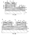
- FIG. 4A is a cross sectional view of the VCSEL shown in FIG. 1 taken along line A-A.
- FIG. 4B is a cross sectional view of the VCSEL shown in FIG. 1 taken along line B-B.
- the p-side electrode and the n-side electrode are omitted in FIG. 4B .
- the cross sectional views are not necessarily shown on the same scale as the plan view shown in FIG. 1 .
- semiconductor thin films are stacked in an order described below; an n-type lower multilayer reflective mirror (hereinafter, lower DBR) 40, spacer layers 42 (layer nearer to the substrate is 42a, farther is 42b), a quantum well active layer 44, a p-type oxidation control layer 46, a p-type upper multilayer reflective mirror (hereinafter, upper DBR) 48.
- the lower DBR 40 and the upper multilayer reflective mirror 48 are distributed Bragg reflectors, and form a vertical resonator structure on the substrate.
- the spacer layers 42 are formed on both upper and lower sides of the substrate, sandwiching the quantum well active layer 44, and thus the layer nearer to the substrate is indicated as 42a, and farther as 42b.
- a p-type contact layer 50 is formed on an upper layer of the upper DBR 48.
- an annular contact electrode 52 is formed.
- An opening 52a in the contact electrode 52 becomes an emission window of laser light.
- a cylindrical mesa portion (or post) 24 is formed on the substrate 22.
- the periphery of a top portion, a sidewall, and a bottom portion of the mesa portion 24 is covered and protected with an interlayer insulating film 54.
- a round-shaped contact hole 54a for exposing a portion of the contact electrode 52 is formed in the interlayer insulating film 54.
- the surface protecting film 32 is formed to cover the whole surface of the substrate.
- a round-shaped contact hole 32a for exposing the contact hole 54a in the interlayer insulating film 54 is formed in the surface protecting film 32.
- the contact hole 32a has a slightly larger diameter than that of the contact hole 54a.
- the separation groove 30 for separating the mesa portion 24 from another mesa portion 24 is formed by etching. There is no limitation for shape, width or the like of the separation groove 30; however, a surface of the interlayer insulating film 54 is exposed by the separation groove 30.
- the p-side electrode 26 is connected to the contact electrode 52 exposed by the contact hole 32a in the surface protecting film 32 and the contact hole 54a in the interlayer insulating film 54.
- the n-side electrode 28 is electrically connected to the n-type lower DBR 40 exposed by the contact holes 54b and 32b respectively formed in the interlayer insulating film 54 and in the surface protecting film 32, at a bottom portion of the mesa portion 24.
- the separation groove 30 for separating between the mesa portions is formed in the surface protecting film 32. Therefore, the stress that may otherwise propagate in the surface protecting film 32 to the inside of the device can be blocked, thereby the stress that occurs between an oxidized region 46a in the oxidation control layer 46 and the interlayer insulating film 54 can be reduced, and resulting degradation in long-term reliability of the VCSEL array device can be suppressed. Especially when any warping occurs on the substrate, for example, due to the difference in coefficient of thermal expansion between the substrate and the semiconductor thin films stacked thereon, stress tends to propagate through the surface protecting film 32; however, by the effect of the separation groove 30, the propagation of the stress can be suppressed.
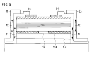
- FIG. 5 illustrates the relation between a normal stress in the interlayer insulating film and a normal stress in the surface protecting film.
- the surface protecting film 32 is a film material having a normal stress f2 in an opposite direction to the normal stress f1.
- the surface protecting film 32 is a film material having a normal stress f2 in a direction in which the film 32 is compressed.
- a preferable combination of materials, film thickness or the like of the interlayer insulating film 54 and the surface protecting film 32 may be selected to satisfy the relationship described above. This enables that even if the stress from the interlayer insulating film 54 propagates in the surface protecting film 32, all or a portion of the normal stress f1 in the interlayer insulating film 54 may be cancelled, and the propagation of the stress into each layer in the mesa portion 24 can be reduced.
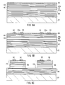
- FIGs. 6A to 7C correspond to the portion shown in FIG. 4B .
- the n-type lower multilayer reflective mirror (DBR) 40 may be formed on the GaAs substrate 12 by alternately stacking plural periods (pairs) of Al 0.9 Ga 0.1 As layer and Al 0.3 Ga 0.7 As layer, for example, wherein the thickness of each layer is ⁇ /4n r (where ⁇ is the lasing wavelength, and n r is the refractive index of the medium).
- the spacer layers 42 may be made of an undoped Al 0.5 Ga 0.5 As, for example, and the quantum well active layer 44 may be made of an undoped GaAs quantum well layer and an undoped Al 0.2 Ga 0.8 As barrier layer, for example.
- the combined thickness of the spacer layers 42 and the quantum well active layer 44 is ⁇ /n r .
- the p-type upper multilayer reflective mirror (DBR) 48 may be formed by alternately stacking plural periods of Al 0.9 Ga 0.1 As layer and Al 0.3 Ga 0.7 As layer, for example, wherein the thickness of each layer is 1/4 of the wavelength in the medium, as in the case of the lower multilayer reflective mirror 40.
- the DBR 48 Formed below the DBR 48 is the p-type AlAs layer (oxidation control layer) 46, and formed on the DBR 48 is the p-type GaAs contact layer 50 having a higher carrier concentration, for example, and these layers 46 and 50 also configure a portion of the reflective mirror.
- the p-type AlAs layer (oxidation control layer) 46 Formed below the DBR 48 is the p-type AlAs layer (oxidation control layer) 46, and formed on the DBR 48 is the p-type GaAs contact layer 50 having a higher carrier concentration, for example, and these layers 46 and 50 also configure a portion of the reflective mirror.
- the annular contact electrode 52 is formed at a top portion of the contact layer 50.
- the contact electrode 52 may be formed of two layers of Ti/Au, for example.
- the electrode 52 has an annular shape, because it acts an opening from which laser light is emitted.
- a predetermined mask pattern is formed on the substrate.
- semiconductor layers may be etched by a reactive ion etching from the upper multilayer reflective mirror 48 to the spacer layer 42a or to a portion of the lower multilayer reflective mirror 40, to form plural cylindrical or rectangular mesa portions (posts) 24. In this example, two cylindrical mesa portions 24 are shown.
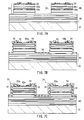
- the substrate is thermally processed under a vapor atmosphere at a high temperature to form an oxidized region 46a surrounding the oxidation control layer (AlAs layer) 46 in the mesa portions 24, as shown in FIG. 7A .
- a current confining layer 46b that also acts as a light confining region is formed at an inner portion of the oxidation control layer 46.
- the interlayer insulating film 54 is formed on the whole surface of the substrate.
- the contact hole 54a in which only an inner portion of the contact electrode 52 is removed, is formed at a top portion of the mesa portion 24.
- the etching of the interlayer insulating film 54 may be performed by using a mask pattern formed by a known photolithography process.
- an inorganic insulating film of such as aluminum nitride (AIN), alumina (Al 2 O 3 ), silicon nitride (SiN x ) or the like may be used.
- an insulating material containing aluminum has a high thermal conductivity, and is preferable for the material of the interlayer insulating film.
- the interlayer insulating film 54 may be a single layer of AlN, or may be stacked layered films in which inorganic insulating films of Al 2 O 3 , SiN x or the like are combined.
- the surface protecting film 32 whose stress (normal stress f2) has an opposite direction to the direction of the normal stress f1 in the interlayer insulating film 54 is formed on the interlayer insulating film 54 and on the whole surface of the substrate.
- the surface protecting film 32 is etched such that the contact hole 32a greater (wider) than the contact hole 54a in the interlayer insulating film 54 is formed.
- the separation groove 30 for separating each of the mesa portions 24 may be formed in the surface protecting film 32 by etching. The etching of the surface protecting film 32 may be performed by using a mask pattern formed by a known photolithography process.
- silicon nitride (SiN x ), silicon dioxide (SiO 2 ), silicon oxynitride (SiON) or the like may be used.
- silicon nitride (SiN x ) for the surface protecting film 32 because of the relation between normal stresses.
- silicon nitride (SiN x ) is used for the interlayer insulating film 54, it is desirable to use silicon dioxide (SiO 2 ) or silicon oxynitride (SiON) for the film 32.
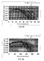
- FIGs. 8A and 8B illustrate examples for comparing the reliability of a VCSEL array device according to an example with that of a related art, under a high-temperature burn-in test.
- a point where the optical output decreases by 2 dB (about 37% down) when a constant current is injected is defined as a failure, and the duration until half of the devices under the test is subjected to failure is defined as mean time to failure Ft.
- FIG. 8A illustrates results for the mean time to failure Ft obtained by a configuration of a related art in which the surface protecting film 32 is formed continuously and there is no separation groove.
- the mean time to failure Ft of the VCSEL array device having the configuration of the related art is about 120 hours, while the mean time to failure Ft of the VCSEL array device of the example is about 180 hours, and it can be seen that the mean time to failure of the VCSEL array device according to the example is increased by about 50%, and the reliability of the device is improved.
- AlN, Al 2 O 3 or the like used for the interlayer insulating film 54 has a high thermal conductivity and a good heat dissipation property, and thus the heat emitted together with light from the quantum well active layer 44 can be efficiently released outside through the interlayer insulating film 54.
- This improves properties of the VCSEL device at a high temperature, and the maximum oscillation temperature is improved by 20%, from 100 degrees centigrade to 120 degrees centigrade (not shown). As a result, stable operation can be maintained even in operating at a high temperature.
- the separation groove is formed only in the surface protecting film, while in the second example, a separation groove is formed in a surface protecting film and an interlayer insulating film below thereof.
- FIG. 9 illustrates a cross section of an essential portion of a VCSEL array device according to a second example. Same reference numerals are used for a similar configuration to that of FIG. 4B .
- a separation groove 30a of the second example penetrates through the surface protecting film 32 and also the interlayer insulating film 54, and reaches a surface of the semiconductor.
- an aim of the present invention is to relieve stress or suppress the occurrence of the stress by providing the surface protecting film 32 having a normal stress in an opposite direction to the normal stress in the interlayer insulating film 54.
- it is difficult to completely eliminate the stress and thus it is expected that the stress may propagate in the interlayer insulating film 54. Therefore, by cutting the film 54 or forming a slit in the film 54 similarly to the surface protecting film 32, the propagation of the stress in the interlayer insulating film 54 may be blocked, which improves long-term reliability.
- the space between the mesa portions including the separation groove 30a may be filled with a resin 60 of polyimide or the like.
- Polyimide being an organic polymer and including an imide bond has a high elasticity as compared with an inorganic insulating film, and stress rarely occurs between the resin 60 and the surface protecting film 32 that comes in contact with the resin 60.
- polyimide does not mediate stress propagation, and has less adverse effect on long-term reliability due to stress.
- polyimide has a low thermal conductivity and has moisture absorbency, and thus there may be another concern in the use under an environment at a high temperature and high humidity.
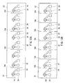
- FIGs. 11A and 11B illustrate plan views of a VCSEL array device according to a fourth example of the present invention.
- plural grooves 70A are formed along a longitudinal direction of the substrate 22 on which array devices are formed.
- the grooves 70A do not completely separate the surface protecting film 32.
- each of the grooves 70A is a slit having a constant length and partitioning the substrate 22 orthogonally to the longitudinal direction of the substrate 22.
- the surface protecting film 32 remains unseparated (intact) at both edge portions of the width of the substrate 22.
- the grooves 70A having such a configuration relieve the stress in the interlayer insulating film similarly to the first to third examples, and also reduce the region exposed by the grooves 70A. Therefore, moisture or water does not easily enter from outside, and moisture resistance and water resistance can be improved.
- FIG. 11B is a modification of the fourth example.
- each of grooves 70B formed between the mesa portions is not a single slit, but has plural slits.
- each of the grooves 70B has three slits lying across the substrate 22, and the three slits are disposed between the mesa portions located in a longitudinal direction of the substrate. The region exposed by the grooves 70B is further reduced, and thus moisture resistance and water resistance of the array device can be improved.
- FIGs. 12A and 12B illustrate plan views of a VCSEL array device according to a fifth example of the present invention.
- n-1 separation grooves are formed when the number of the mesas is n; however, in the fifth example, the number of the grooves is not limited to n-1, and fewer grooves may be formed.
- grooves 70C are formed between every two mesa portions, excepting the mesa portions locating at the rightmost and leftmost. This is only exemplary, and, for example, in a case where the number of the mesa portions formed in a longitudinal direction of the substrate 22 is quite large, the grooves may be formed at intervals of every three or greater than three mesa portions.
- the pattern of the grooves is not necessarily limited to one type; but plural patterns may be formed.
- grooves 70D each having plural slits are formed between every two mesa portions, and linear grooves 70E are formed between every two mesa portions, and each of the grooves 70D and grooves 70E are alternately arranged in a longitudinal direction of the substrate 22.
- FIGs. 13A and 13B illustrate cross sections of an essential portion of a VCSEL array according to a sixth example of the present invention.
- a groove 70F formed at a certain depth in the surface protecting film 32 does not completely separate (cut through) the surface protecting film 32.
- the groove 70F having a desired depth can be obtained, for example, by adjusting the time of etching.
- the groove 70F does not expose the underlying interlayer insulating film 54, and thus moisture or water penetration from the groove 70F into the interlayer insulating film 54 may be suppressed, and moisture resistance and water resistance of the array device can be improved.
- the cross sectional shape of the groove may be made in a tapered shape.
- the tapered shape may be formed by an isotropic wet etching, for example.
- the groove 70G has a sloped step, and thus stress concentration at the step may be relieved.
- the adhesion of the surface protecting film 32 to the interlayer insulating film 54 may also be improved. Another advantage is that, in a case where the groove 70G is filed with a filling resin as shown in FIG. 10 , void occurrence in the groove 70G may be avoided because the groove is sloped.
- FIG. 14 illustrates a cross section of an essential portion of a VCSEL array according to a seventh example of the present invention.
- the seventh example is a modification of the third example shown in FIG. 10 .
- the groove 70G formed in the surface protecting film 32 and the interlayer insulating film 54 is filled with a filling resin 60A; however, not all the space between the mesa portions is filled.
- thermal stress which otherwise the resin 60A may cause near the oxidation control layer in the mesa portion, can be reduced.
- FIG. 15 illustrates a cross section of an essential portion of a VCSEL array according to an eighth example of the present invention.
- the space between the mesa portions is filled with an insulating material 80 of polyimide or the like, and the area between the mesa portions 24 is planarized.
- An interlayer insulating film 54B and a surface protecting film 32B are formed on the planarized insulating material 80, and a groove 70H is formed in the surface protecting film 32B.
- FIG. 16 illustrates a cross section of an essential portion of a VCSEL array according to a ninth example of the present invention.
- FIG. 16 corresponds to the cross section of FIG. 1 taken along line B-B.
- the ninth example differs from the first example (see FIG. 4B ), and an in-between mesa portion 24A is formed between the light-emitting mesa portions 24.
- the in-between mesa portion 24A has a same semiconductor stacked layered configuration as the mesa portions 24, and an electrode layer is wired to a top portion of the mesa portion 24A.
- grooves 70J are formed in the surface protecting film 32 at a bottom portion of the mesa portions, and a groove 70K is formed in the surface protecting film 32 at a top portion of the mesa of the in-between mesa portion 24A.
- the grooves 70J are located in proximity to the mesa portions 24, and thus the stress in the interlayer insulating film 54 can be effectively relieved.
- the groove 70K is located away from the mesa portions 24, and thus the path of the moisture or water penetrating therefrom into the mesa portions 24 becomes longer. This is effective in improving moisture resistance and water resistance of the mesa portions 24.
- Both grooves 70J and 70K are not necessarily formed: either the groove 70J or the groove 70K is sufficient.
- the formation of a surface protecting film and the formation of a groove or a separation groove may relieve the stress in an interlayer insulating film, whereby the reliability of the device can be improved.
- the number, shape or the like of the groove or separation groove can be changed as appropriate in accordance with purpose or use.
- a VCSEL array device may be applied to a light emitting device such as an LED or a laser diode in which arrays may be arranged one-dimensionally or two-dimensionally on a substrate, and can be used as a light source for optical transmission, optical storage or the like.
- a light emitting device such as an LED or a laser diode in which arrays may be arranged one-dimensionally or two-dimensionally on a substrate, and can be used as a light source for optical transmission, optical storage or the like.
Landscapes
- Physics & Mathematics (AREA)
- Condensed Matter Physics & Semiconductors (AREA)
- General Physics & Mathematics (AREA)
- Electromagnetism (AREA)
- Optics & Photonics (AREA)
- Semiconductor Lasers (AREA)
Abstract
Provided is a VCSEL array device (20) that includes at least a first multilayer reflective film, an active layer, and a second multilayer reflective film, formed on a substrate (22) that extends in a longitudinal direction. Plural mesa portions (24) are formed on the substrate by selectively removing at least a portion of the first multilayer reflective film, active layer, and second multilayer reflective film. A selectively oxidized region is formed in at least one of the first multilayer reflective film and the second multilayer reflective film. The VCSEL array device further includes an interlayer insulating film that covers at least a side portion and a bottom portion of the mesa portions, and a surface protecting film (32) that covers the interlayer insulating film. The surface protecting film (32) has plural grooves (30) formed along a longitudinal direction of the substrate in which at least a portion of the surface protecting film is removed.
Description
- This invention relates to a surface light emitting semiconductor array device, and more specifically, to a stacked layered configuration of a Vertical-Cavity Surface-Emitting Laser diode (hereinafter referred to as VCSEL) array device. This invention also relates to a method for manufacturing the VCSEL array device.
- A VCSEL device is a type of laser diode that emits light from a surface of a semiconductor substrate. VCSELs have excellent characteristics, which edge-emitting type laser diodes do not have. For example, VCSELs require a lower current value for their driving (lower threshold current), and property tests can be performed while VCSELs are on a wafer (nondestructive evaluation), and VCSELs can be easily arranged in two-dimensional arrays. With these characteristics, VCSELs have been used as light sources for an optical data processor or an optical communication device, or a data storage apparatus using light.
-
FIG. 17 schematically illustrates a configuration of a selective oxidation type VCSEL device disclosed inJP-A-2004-200211 substrate 1 are; n-type lower DBR layers 3: p-type upper DBR layers 9:active regions 7 disposed between the upper and lower DBR layers: and a current confining layer 8 that includes an oxidized region 8b being selectively oxidized. A contact layer 10, the upper DBR layers 9, and the current confining layer 8 form a mesa structure on the substrate. An edge portion of an upper surface and a side surface of the mesa structure, and a mesa bottom portion are covered with aninterlayer insulating film 13. For the oxidation type VCSEL device disclosed inJP-A-2004-200211 interlayer insulating film 13 is set to be equal to or less than 1.5 x 10⁹ (dyne/cm2) in order to prevent release of the mesa structure or the like and extend device life. For the oxidation type VCSEL device disclosed inJP-A-2004-200211 interlayer insulating film 13 is set to be equal to or less than 1.5 x 10⁹ (dyne/cm2) in order to prevent release of the mesa structure or the like and extend device life. - In
JP-A-2004-241777 - In
JP-A-2006-086498 - An issue with selective oxidation type VCSEL devices is so-called sudden failure. It has been thought that the cause of the sudden failure is that the composition in a stacked layered material alters due to oxidation, which causes dislocations (point defects) in a stacked film. The heat generated by laser oscillation enhances the movements of the dislocations and increases the dislocations, and the dislocations penetrate into an active layer and induce a sudden failure (device degradation). However, further studies have found that the dislocations do not occur simply due to the oxidation, but internal stresses occurred between an oxidized region and an interlayer insulating film formed near the oxidized region is a cause of the sudden failure.
- A semiconductor layer that becomes a base of a VCSEL and an interlayer insulating film made of a dielectric film each has a different coefficient of thermal expansion, and thus it is inevitable that stress will occur as temperature rises. Such stress occurrence is especially noticeable in a long array device (that has plural light emitting points) in which stress is easily caused inherently due to warping of the substrate, and such stress occurrence has to be addressed.
- It is therefore desirable to provide a VCSEL device in which life degradation due to stress may be suppressed by controlling the stress that occurs in an interlayer insulating film, so that the reliability of the device is improved, and to provide a method for manufacturing a VCSEL device.
- An aspect of the present invention provides a VCSEL array device that includes at least a first multilayer reflective film, an active layer, and a second multilayer reflective film, formed on a substrate that extends in a longitudinal direction. Plural mesa portions are formed on the substrate by selectively removing at least a portion of the first multilayer reflective film, active layer, and second multilayer reflective film. A selectively oxidized region is formed in at least one of the first multilayer reflective film and the second multilayer reflective film. The VCSEL array device further includes an interlayer insulating film that covers at least a side portion and a bottom portion of the mesa portions, and a surface protecting film that covers the interlayer insulating film. The surface protecting film has plural grooves formed along a longitudinal direction of the substrate in which at least a portion of the surface protecting film is removed.
- The grooves may be formed to reach the surface protecting film and the interlayer insulating film directly below the surface protecting film. The groove may comprise a slit formed across the substrate. Preferably, the number of the grooves is at least n-1 when the number of the mesa portions linearly arranged is n (n is a natural number equal to or greater than 2). For example, at least seven grooves are formed when eight mesa portions (light emitting portion) are arranged linearly. Preferably, the interlayer insulating film is a single inorganic insulating film or stacked layered films made of a plurality of inorganic insulating films of different materials. Preferably, the surface protecting film is an insulating film of a film material having a normal stress in an opposite direction to the direction of the normal stress in the interlayer insulating film. Preferably, the interlayer insulating film is made of an inorganic insulating film in which at least one layer thereof comprises aluminum. The interlayer insulating film may be stacked layered films made of an inorganic insulating film that comprises aluminum and an inorganic insulating film that comprises silicon. Preferably, the first and second multilayer reflective films are III-V group semiconductor layers that comprise Al, and the selectively oxidized region is a semiconductor layer that comprises Al selectively oxidized from a side surface of the mesa portion. Preferably, the grooves are filled with an insulating material.
- An aspect of the present invention provides a method for manufacturing a Vertical-Cavity Surface-Emitting Laser diode (VCSEL) array device that includes the steps of forming at least a first multilayer reflective film, an active layer, and a second multilayer reflective film, on a substrate extending in a longitudinal direction, forming a plurality of mesa portions on the substrate by etching at least a portion of the first multilayer reflective film, the active layer, and the second multilayer reflective film, forming an oxidized region selectively oxidized from a side surface of the plurality of mesa portions, forming an interlayer insulating film on the substrate to cover at least a side portion and a bottom portion of the plurality of mesa portions, forming a surface protecting film on the interlayer insulating film, and forming a plurality of grooves in the surface protecting film along a longitudinal direction of the substrate by removing at least a portion of the surface protecting film.
- According to an aspect of the present invention, the inner stress that may occur between an oxidized region provided near an active layer and an interlayer insulating film may be relieved as compared with a structure in which a groove is not formed in a surface protecting film that is formed to cover the interlayer insulating film, and thus the increase of dislocations in a stacked material may be suppressed, and a highly reliable VCSEL array device can be obtained.
- Regarding the increase of temperature near the active layer due to heat generation, the heat generated from the active layer may be effectively released outside, as compared with a structure in which an insulating film mainly made of aluminum that has a high heat dissipation property is not used for an interlayer insulating film that covers the side surface of a mesa portion.
- Exemplary embodiments of the present invention will be described in detail based on the following figures, wherein:
-
FIG. 1 is a plan view illustrating a configuration of a VCSEL device in which mesa portions are linearly arranged according to an example of the present invention; -
FIG. 2 illustrates other examples of separation grooves formed on the substrate; -
FIG. 3 is a plan view illustrating a configuration of a VCSEL device in which mesa portions are two-dimensionally arranged according to an example of the present invention; -
FIG. 4A illustrates a cross section of the VCSEL device shown inFIG. 1 taken along line A-A; -
FIG. 4B illustrates a cross section of a VCSEL device shown inFIG. 1 taken along line B-B (excepting electrode); -
FIG. 5 illustrates the relation between a normal stress in an interlayer insulating film and a normal stress in a surface protecting film; -
FIGs. 6A to 6C are cross sectional views illustrating a process for manufacturing a VCSEL array device according to an example of the present invention; -
FIGs. 7A to 7C are cross sectional views illustrating a process for manufacturing a VCSEL array device according to an example of the present invention; -
FIGs. 8A and 8B are graphs illustrating results of a high-temperature burn-in test, comparing a VCSEL array device according to an example of the present invention with a VCSEL array device of a related art; -
FIG. 9 illustrates a cross section of an essential portion of a VCSEL array device according to a second example of the present invention; -
FIG. 10 illustrates a cross section of an essential portion of a VCSEL array device according to a third example of the present invention; -
FIGs. 11A and 11B are plan views illustrating a configuration of a VCSEL device according to a fourth example of the present invention in which mesa portions are linearly arranged; -
FIGs. 12A and 12B are plan views illustrating a configuration a VCSEL array device according to a fifth example of the present invention in which mesa portions are linearly arranged; -
FIGs. 13A and 13B illustrate cross sections of an essential portion of an array device according to a sixth example of the present invention; -
FIG. 14 illustrates a cross section of an essential portion of an array device according to a seventh example of the present invention; -
FIG. 15 illustrates a cross section of an essential portion of an array device according to an eighth example of the present invention; -
FIG. 16 illustrates a cross section of an essential portion of an array device according to a ninth example of the present invention; and -
FIG. 17 illustrates a cross section of a configuration of a VCSEL device of a related art. - Referring to the accompanying drawings, examples of a selective oxidation type VCSEL array device according to an aspect of the present invention will be now described.
-
FIG. 1 is a schematic plan view of an array device of a selective oxidation type VCSEL according to an example of the present invention. In anarray device 20 shown inFIG. 1 , plural mesa portions 24 (light emitting portions) are arranged linearly on an oblongrectangular substrate 22. On the substrate, eightmesa portions 24 may be formed at an approximate constant interval. On the substrate, plural p-side electrodes 26 and plural n-side electrodes 28 may be formed corresponding to themesa portions 24. The p-side electrode 26 is electrically connected to a p-type contact layer at a top portion of themesa portion 24. The n-side electrode 28 is electrically connected to an n-type semiconductor layer of themesa portion 24. When a forward bias current is applied to the p-side electrode 26 and the n-side electrode 28, laser light is emitted from a top portion ofcorresponding mesa portion 24. In the example shown inFIG. 1 , plural p-side electrodes 26 and plural n-side electrodes 28 are shown, however, in a case where all themesa portions 24 are concurrently driven, the plural p-side electrodes 26 may be replaced with a common single electrode, and the plural n-side electrodes 28 may be replaced with a common single electrode. - On a surface of the substrate, a
surface protecting film 32 for protecting themesa portions 24 is formed. In this example,separation grooves 30 for separating each of the mesa portions are formed in thesurface protecting film 32. Preferably, when n (n is a natural number equal to or greater than 2)mesa portions 24 are linearly arranged on the substrate, at least n-1separation grooves 30 are formed for separating each of themesa portions 24. However, the number of the separation grooves to be formed between one mesa portion and a mesa portion adjacent thereto may be either one or more than one. In the example ofFIG. 1 , sevenseparation grooves 30 are formed for the linearly arranged eight mesa portions. - The
separation groove 30 may extend across thesurface protecting film 32 and completely separate thesurface protecting film 32 as shown inFIG. 1 , or may partially separate thesurface protecting film 32. The shape of theseparation groove 30 may be linear; however, as shown inFIG. 2 , the shape may be acurve 31a, a shape that includes abent portion 31b, or a shape that includes anorthogonal portion 31c. In the example ofFIG. 1 , theseparation grooves 30 extend linearly in parallel each other, having a constant angle with respect to a longitudinal direction of the substrate, and completely separate thesurface protecting film 32. -
FIG. 3 is a schematic plan view of an array device in which plural mesa portions (light emitting portions) are two-dimensionally arranged. Themesa portions 24 are arranged in an arrangement of 5 by 2 along a longitudinal direction of therectangular substrate 22. Theseparation grooves 30 are formed for separating each of the mesa portions, four in a lengthwise direction, and one in a widthwise direction. Preferably, when the arrangement of themesa portions 24 is n by m (n and m are natural numbers), the number of the separation grooves in a lengthwise direction is at least n-1, and the number of the separation grooves in a widthwise direction is at least m-1. - A configuration of a VCSEL array device will be now described in detail.
FIG. 4A is a cross sectional view of the VCSEL shown inFIG. 1 taken along line A-A.FIG. 4B is a cross sectional view of the VCSEL shown inFIG. 1 taken along line B-B. For the sake of convenience, the p-side electrode and the n-side electrode are omitted inFIG. 4B . In addition, the cross sectional views are not necessarily shown on the same scale as the plan view shown inFIG. 1 . - On the
semiconductor substrate 22 having a semiinsulating property, semiconductor thin films are stacked in an order described below; an n-type lower multilayer reflective mirror (hereinafter, lower DBR) 40, spacer layers 42 (layer nearer to the substrate is 42a, farther is 42b), a quantum wellactive layer 44, a p-typeoxidation control layer 46, a p-type upper multilayer reflective mirror (hereinafter, upper DBR) 48. Thelower DBR 40 and the upper multilayerreflective mirror 48 are distributed Bragg reflectors, and form a vertical resonator structure on the substrate. The spacer layers 42 are formed on both upper and lower sides of the substrate, sandwiching the quantum wellactive layer 44, and thus the layer nearer to the substrate is indicated as 42a, and farther as 42b. On an upper layer of theupper DBR 48, a p-type contact layer 50 is formed. In thecontact layer 50, anannular contact electrode 52 is formed. Anopening 52a in thecontact electrode 52 becomes an emission window of laser light. - By etching the semiconductor thin films from the
upper DBR 48 to the spacer layer 42 or to thelower DBR 40, a cylindrical mesa portion (or post) 24 is formed on thesubstrate 22. The periphery of a top portion, a sidewall, and a bottom portion of themesa portion 24 is covered and protected with aninterlayer insulating film 54. At a top portion of themesa portion 24, a round-shapedcontact hole 54a for exposing a portion of thecontact electrode 52 is formed in theinterlayer insulating film 54. - On the
interlayer insulating film 54, thesurface protecting film 32 is formed to cover the whole surface of the substrate. At a top portion of themesa portion 24, a round-shapedcontact hole 32a for exposing thecontact hole 54a in theinterlayer insulating film 54 is formed in thesurface protecting film 32. Thecontact hole 32a has a slightly larger diameter than that of thecontact hole 54a. In thesurface protecting film 32, as shown inFIG. 1 , theseparation groove 30 for separating themesa portion 24 from anothermesa portion 24 is formed by etching. There is no limitation for shape, width or the like of theseparation groove 30; however, a surface of theinterlayer insulating film 54 is exposed by theseparation groove 30. - As shown in
FIG. 4A , at a top portion of themesa portion 24, the p-side electrode 26 is connected to thecontact electrode 52 exposed by thecontact hole 32a in thesurface protecting film 32 and thecontact hole 54a in theinterlayer insulating film 54. The n-side electrode 28 is electrically connected to the n-typelower DBR 40 exposed by the contact holes 54b and 32b respectively formed in theinterlayer insulating film 54 and in thesurface protecting film 32, at a bottom portion of themesa portion 24. - In the VCSEL array device according to the example, the
separation groove 30 for separating between the mesa portions is formed in thesurface protecting film 32. Therefore, the stress that may otherwise propagate in thesurface protecting film 32 to the inside of the device can be blocked, thereby the stress that occurs between anoxidized region 46a in theoxidation control layer 46 and theinterlayer insulating film 54 can be reduced, and resulting degradation in long-term reliability of the VCSEL array device can be suppressed. Especially when any warping occurs on the substrate, for example, due to the difference in coefficient of thermal expansion between the substrate and the semiconductor thin films stacked thereon, stress tends to propagate through thesurface protecting film 32; however, by the effect of theseparation groove 30, the propagation of the stress can be suppressed. -
FIG. 5 illustrates the relation between a normal stress in the interlayer insulating film and a normal stress in the surface protecting film. When warping stress due to the oxidizedregion 46a in theoxidation control layer 46 near theactive layer 44 causes a normal stress f1 in theinterlayer insulating film 54 such that thefilm 54 is compressed normal to themesa portion 24 as illustrated, it is preferable that thesurface protecting film 32 is a film material having a normal stress f2 in an opposite direction to the normal stress f1. In contrast, if the normal stress f1 in theinterlayer insulating film 54 has a direction such that thefilm 54 is stretched, it is preferable that thesurface protecting film 32 is a film material having a normal stress f2 in a direction in which thefilm 32 is compressed. A preferable combination of materials, film thickness or the like of theinterlayer insulating film 54 and thesurface protecting film 32 may be selected to satisfy the relationship described above. This enables that even if the stress from theinterlayer insulating film 54 propagates in thesurface protecting film 32, all or a portion of the normal stress f1 in theinterlayer insulating film 54 may be cancelled, and the propagation of the stress into each layer in themesa portion 24 can be reduced. - Referring now to
FIGs. 6A to 7C , a method for manufacturing a VCSEL array device will be described.FIGs. 6A to 7C correspond to the portion shown inFIG. 4B . As shown inFIG. 6A , the n-type lower multilayer reflective mirror (DBR) 40 may be formed on the GaAs substrate 12 by alternately stacking plural periods (pairs) of Al0.9Ga0.1As layer and Al0.3Ga0.7As layer, for example, wherein the thickness of each layer is λ/4nr (where λ is the lasing wavelength, and nr is the refractive index of the medium). The spacer layers 42 (42a, 42b) may be made of an undoped Al0.5Ga0.5As, for example, and the quantum wellactive layer 44 may be made of an undoped GaAs quantum well layer and an undoped Al0.2Ga0.8As barrier layer, for example. The combined thickness of the spacer layers 42 and the quantum wellactive layer 44 is λ/nr. The p-type upper multilayer reflective mirror (DBR) 48 may be formed by alternately stacking plural periods of Al0.9Ga0.1As layer and Al0.3Ga0.7As layer, for example, wherein the thickness of each layer is 1/4 of the wavelength in the medium, as in the case of the lower multilayerreflective mirror 40. Formed below theDBR 48 is the p-type AlAs layer (oxidation control layer) 46, and formed on theDBR 48 is the p-typeGaAs contact layer 50 having a higher carrier concentration, for example, and theselayers - As shown in
FIG. 6B , theannular contact electrode 52 is formed at a top portion of thecontact layer 50. Thecontact electrode 52 may be formed of two layers of Ti/Au, for example. Theelectrode 52 has an annular shape, because it acts an opening from which laser light is emitted. - By using a photolithography process, a predetermined mask pattern is formed on the substrate. Then, as shown in
FIG. 6C , semiconductor layers may be etched by a reactive ion etching from the upper multilayerreflective mirror 48 to thespacer layer 42a or to a portion of the lower multilayerreflective mirror 40, to form plural cylindrical or rectangular mesa portions (posts) 24. In this example, twocylindrical mesa portions 24 are shown. - The substrate is thermally processed under a vapor atmosphere at a high temperature to form an oxidized
region 46a surrounding the oxidation control layer (AlAs layer) 46 in themesa portions 24, as shown inFIG. 7A . By this thermal processing, a current confininglayer 46b that also acts as a light confining region is formed at an inner portion of theoxidation control layer 46. - As shown in
FIG. 7B , theinterlayer insulating film 54 is formed on the whole surface of the substrate. Thecontact hole 54a, in which only an inner portion of thecontact electrode 52 is removed, is formed at a top portion of themesa portion 24. The etching of theinterlayer insulating film 54 may be performed by using a mask pattern formed by a known photolithography process. For the material of theinterlayer insulating film 54, an inorganic insulating film of such as aluminum nitride (AIN), alumina (Al2O3), silicon nitride (SiNx) or the like may be used. Especially, an insulating material containing aluminum has a high thermal conductivity, and is preferable for the material of the interlayer insulating film. Theinterlayer insulating film 54 may be a single layer of AlN, or may be stacked layered films in which inorganic insulating films of Al2O3, SiNx or the like are combined. - As shown in
FIG. 7C , thesurface protecting film 32 whose stress (normal stress f2) has an opposite direction to the direction of the normal stress f1 in theinterlayer insulating film 54 is formed on theinterlayer insulating film 54 and on the whole surface of the substrate. At a top portion of themesa portion 24, thesurface protecting film 32 is etched such that thecontact hole 32a greater (wider) than thecontact hole 54a in theinterlayer insulating film 54 is formed. Concurrently with the formation of thecontact hole 32a, as shown inFIG. 4B , theseparation groove 30 for separating each of themesa portions 24 may be formed in thesurface protecting film 32 by etching. The etching of thesurface protecting film 32 may be performed by using a mask pattern formed by a known photolithography process. - For the material of the
surface protecting film 32, silicon nitride (SiNx), silicon dioxide (SiO2), silicon oxynitride (SiON) or the like may be used. For example, if a single layer or stacked layered films of AIN or Al2O3 is used for theinterlayer insulating film 54, it is desirable to use silicon nitride (SiNx) for thesurface protecting film 32 because of the relation between normal stresses. If silicon nitride (SiNx) is used for theinterlayer insulating film 54, it is desirable to use silicon dioxide (SiO2) or silicon oxynitride (SiON) for thefilm 32. -
FIGs. 8A and 8B illustrate examples for comparing the reliability of a VCSEL array device according to an example with that of a related art, under a high-temperature burn-in test. In this disclosure, a point where the optical output decreases by 2 dB (about 37% down) when a constant current is injected is defined as a failure, and the duration until half of the devices under the test is subjected to failure is defined as mean time to failure Ft.FIG. 8A illustrates results for the mean time to failure Ft obtained by a configuration of a related art in which thesurface protecting film 32 is formed continuously and there is no separation groove.FIG. 8B illustrates results obtained by a VCSEL array device according to an example in which theseparation grooves 30 are formed for separating thesurface protecting film 32 between each of themesa portions 24. As obvious from these graphs, the mean time to failure Ft of the VCSEL array device having the configuration of the related art is about 120 hours, while the mean time to failure Ft of the VCSEL array device of the example is about 180 hours, and it can be seen that the mean time to failure of the VCSEL array device according to the example is increased by about 50%, and the reliability of the device is improved. - In addition, AlN, Al2O3 or the like used for the
interlayer insulating film 54 has a high thermal conductivity and a good heat dissipation property, and thus the heat emitted together with light from the quantum wellactive layer 44 can be efficiently released outside through theinterlayer insulating film 54. This improves properties of the VCSEL device at a high temperature, and the maximum oscillation temperature is improved by 20%, from 100 degrees centigrade to 120 degrees centigrade (not shown). As a result, stable operation can be maintained even in operating at a high temperature. - A second example of the present invention will be now described. In the first example, the separation groove is formed only in the surface protecting film, while in the second example, a separation groove is formed in a surface protecting film and an interlayer insulating film below thereof.
-
FIG. 9 illustrates a cross section of an essential portion of a VCSEL array device according to a second example. Same reference numerals are used for a similar configuration to that ofFIG. 4B . As shown inFIG. 9 , aseparation groove 30a of the second example penetrates through thesurface protecting film 32 and also theinterlayer insulating film 54, and reaches a surface of the semiconductor. As described above, an aim of the present invention is to relieve stress or suppress the occurrence of the stress by providing thesurface protecting film 32 having a normal stress in an opposite direction to the normal stress in theinterlayer insulating film 54. However, it is difficult to completely eliminate the stress, and thus it is expected that the stress may propagate in theinterlayer insulating film 54. Therefore, by cutting thefilm 54 or forming a slit in thefilm 54 similarly to thesurface protecting film 32, the propagation of the stress in theinterlayer insulating film 54 may be blocked, which improves long-term reliability. - A third example of the present invention will be now described. In the second example, a portion of the
interlayer insulating film 54 is removed by theseparation groove 30a; however, if the semiconductor surface exposed by the removal of theinterlayer insulating film 54 is exposed to the atmosphere, the exposure may cause oxidation or corrosion. To avoid such a disadvantage, in the third example, as shown inFIG. 10 , the space between the mesa portions including theseparation groove 30a may be filled with aresin 60 of polyimide or the like. Polyimide being an organic polymer and including an imide bond has a high elasticity as compared with an inorganic insulating film, and stress rarely occurs between theresin 60 and thesurface protecting film 32 that comes in contact with theresin 60. Furthermore, polyimide does not mediate stress propagation, and has less adverse effect on long-term reliability due to stress. However, it should be noted that polyimide has a low thermal conductivity and has moisture absorbency, and thus there may be another concern in the use under an environment at a high temperature and high humidity. - Fourth to ninth examples of the present invention will be described, in which same reference numerals have been retained for similar configurations to those of the first to third examples.
-
FIGs. 11A and 11B illustrate plan views of a VCSEL array device according to a fourth example of the present invention. In the fourth example, as shown inFIG. 11A ,plural grooves 70A are formed along a longitudinal direction of thesubstrate 22 on which array devices are formed. Thegrooves 70A do not completely separate thesurface protecting film 32. In other words, each of thegrooves 70A is a slit having a constant length and partitioning thesubstrate 22 orthogonally to the longitudinal direction of thesubstrate 22. Thesurface protecting film 32 remains unseparated (intact) at both edge portions of the width of thesubstrate 22. Thegrooves 70A having such a configuration relieve the stress in the interlayer insulating film similarly to the first to third examples, and also reduce the region exposed by thegrooves 70A. Therefore, moisture or water does not easily enter from outside, and moisture resistance and water resistance can be improved. -
FIG. 11B is a modification of the fourth example. In this example, each ofgrooves 70B formed between the mesa portions is not a single slit, but has plural slits. In the example inFIG. 11B , each of thegrooves 70B has three slits lying across thesubstrate 22, and the three slits are disposed between the mesa portions located in a longitudinal direction of the substrate. The region exposed by thegrooves 70B is further reduced, and thus moisture resistance and water resistance of the array device can be improved. -
FIGs. 12A and 12B illustrate plan views of a VCSEL array device according to a fifth example of the present invention. In the first example, n-1 separation grooves are formed when the number of the mesas is n; however, in the fifth example, the number of the grooves is not limited to n-1, and fewer grooves may be formed. In the example shown inFIG. 12A ,grooves 70C are formed between every two mesa portions, excepting the mesa portions locating at the rightmost and leftmost. This is only exemplary, and, for example, in a case where the number of the mesa portions formed in a longitudinal direction of thesubstrate 22 is quite large, the grooves may be formed at intervals of every three or greater than three mesa portions. In addition, the pattern of the grooves is not necessarily limited to one type; but plural patterns may be formed. For example, as shown inFIG. 12B ,grooves 70D each having plural slits are formed between every two mesa portions, andlinear grooves 70E are formed between every two mesa portions, and each of thegrooves 70D andgrooves 70E are alternately arranged in a longitudinal direction of thesubstrate 22. By reducing the number of the grooves for the number of the mesa portions, the region exposed by the grooves may be reduced, and thus moisture resistance and water resistance can be improved. The stress in the interlayer insulating film is also relieved by the grooves. -
FIGs. 13A and 13B illustrate cross sections of an essential portion of a VCSEL array according to a sixth example of the present invention. In the sixth example, agroove 70F formed at a certain depth in thesurface protecting film 32 does not completely separate (cut through) thesurface protecting film 32. Thegroove 70F having a desired depth can be obtained, for example, by adjusting the time of etching. Thegroove 70F does not expose the underlyinginterlayer insulating film 54, and thus moisture or water penetration from thegroove 70F into theinterlayer insulating film 54 may be suppressed, and moisture resistance and water resistance of the array device can be improved. - As in a
groove 70G shown inFIG. 13B , the cross sectional shape of the groove may be made in a tapered shape. The tapered shape may be formed by an isotropic wet etching, for example. As compared with thegroove 70F having an acute step shown inFIG. 13A , thegroove 70G has a sloped step, and thus stress concentration at the step may be relieved. In addition, the adhesion of thesurface protecting film 32 to theinterlayer insulating film 54 may also be improved. Another advantage is that, in a case where thegroove 70G is filed with a filling resin as shown inFIG. 10 , void occurrence in thegroove 70G may be avoided because the groove is sloped. -
FIG. 14 illustrates a cross section of an essential portion of a VCSEL array according to a seventh example of the present invention. The seventh example is a modification of the third example shown inFIG. 10 . In the seventh example, thegroove 70G formed in thesurface protecting film 32 and theinterlayer insulating film 54 is filled with a fillingresin 60A; however, not all the space between the mesa portions is filled. By limiting the amount of the fillingresin 60A, thermal stress, which otherwise theresin 60A may cause near the oxidation control layer in the mesa portion, can be reduced. -
FIG. 15 illustrates a cross section of an essential portion of a VCSEL array according to an eighth example of the present invention. In the eighth example, the space between the mesa portions is filled with an insulatingmaterial 80 of polyimide or the like, and the area between themesa portions 24 is planarized. An interlayer insulatingfilm 54B and asurface protecting film 32B are formed on the planarized insulatingmaterial 80, and agroove 70H is formed in thesurface protecting film 32B. By planarizing the area between the mesa portions, theinterlayer insulating film 54B and thesurface protecting film 32B can be easily formed, and the film thickness of these films can be made thinner. -
FIG. 16 illustrates a cross section of an essential portion of a VCSEL array according to a ninth example of the present invention.FIG. 16 corresponds to the cross section ofFIG. 1 taken along line B-B. The ninth example differs from the first example (seeFIG. 4B ), and an in-betweenmesa portion 24A is formed between the light-emittingmesa portions 24. The in-betweenmesa portion 24A has a same semiconductor stacked layered configuration as themesa portions 24, and an electrode layer is wired to a top portion of themesa portion 24A. In such an array device configuration,grooves 70J are formed in thesurface protecting film 32 at a bottom portion of the mesa portions, and agroove 70K is formed in thesurface protecting film 32 at a top portion of the mesa of the in-betweenmesa portion 24A. Thegrooves 70J are located in proximity to themesa portions 24, and thus the stress in theinterlayer insulating film 54 can be effectively relieved. In addition, thegroove 70K is located away from themesa portions 24, and thus the path of the moisture or water penetrating therefrom into themesa portions 24 becomes longer. This is effective in improving moisture resistance and water resistance of themesa portions 24. Bothgrooves groove 70J or thegroove 70K is sufficient. - As described above, in a VCSEL array device according to the examples described above, the formation of a surface protecting film and the formation of a groove or a separation groove may relieve the stress in an interlayer insulating film, whereby the reliability of the device can be improved. The number, shape or the like of the groove or separation groove can be changed as appropriate in accordance with purpose or use. In addition, it is also possible to combine each of the examples from the first to the ninth examples described above.
- The foregoing description of the examples has been provided for the purposes of illustration and description, and it is not intended to limit the scope of the invention. It should be understood that the invention may be implemented by other methods within the scope of the invention that satisfies requirements of a configuration of the present invention.
- According to an aspect of the present invention, a VCSEL array device may be applied to a light emitting device such as an LED or a laser diode in which arrays may be arranged one-dimensionally or two-dimensionally on a substrate, and can be used as a light source for optical transmission, optical storage or the like.
Claims (14)
- A Vertical-Cavity Surface-Emitting Laser diode (VCSEL) array device, comprising:a substrate extending in a longitudinal direction,at least a first multilayer reflective film, an active layer, and a second multilayer reflective film, formed on the substrate,a plurality of mesa portions formed on the substrate by selectively removing at least a portion of the first multilayer reflective film, the active layer, and the second multilayer reflective film,a selectively oxidized region formed in at least one of the first multilayer reflective film and the second multilayer reflective film,an interlayer insulating film covering at least a side portion and a bottom portion of the mesa portions, anda surface protecting film covering the interlayer insulating film,the surface protecting film having a plurality of grooves formed along a longitudinal direction of the substrate in which at least a portion of the surface protecting film is removed.
- The VCSEL array device according to claim 1, wherein the grooves are formed to reach the surface protecting film and the interlayer insulating film directly below the surface protecting film.
- The VCSEL array device according to claim 1 or 2, wherein the groove comprises a slit formed across the substrate.
- The VCSEL array device according to any one of claims 1 to 3, wherein the number of the grooves is at least n-1 when the number of the mesa portions linearly arranged is n (n is a natural number equal to or greater than 2).
- The VCSEL array device according to any one of claims 1 to 4, wherein the interlayer insulating film is a single inorganic insulating film or stacked layered films made of a plurality of inorganic insulating films of different materials.
- The VCSEL array device according to any one of claims 1 to 5, wherein the surface protecting film is an insulating film of a film material having a normal stress in an opposite direction to the direction of the normal stress in the interlayer insulating film.
- The VCSEL array device according to any one of claims 1 to 6, wherein the interlayer insulating film is made of an inorganic insulating film in which at least one layer thereof comprises aluminum.
- The VCSEL array device according to any one of claims 1 to 6, wherein the interlayer insulating film is stacked layered films made of an inorganic insulating film that comprises aluminum and an inorganic insulating film that comprises silicon.
- The VCSEL array device according to any preceding claim, wherein the grooves are filled with an insulating material.
- The VCSEL array device according to any one of claims 1 to 9, wherein the first and second multilayer reflective films are III-V group semiconductor layers that comprise Al, and the selectively oxidized region is a semiconductor layer that comprises Al selectively oxidized from a side surface of the mesa portion.
- A method for manufacturing a Vertical-Cavity Surface-Emitting Laser diode (VCSEL) array device, comprising:forming at least a first multilayer reflective film, an active layer, and a second multilayer reflective film, on a substrate extending in a longitudinal direction,forming a plurality of mesa portions on the substrate by etching at least a portion of the first multilayer reflective film, the active layer, and the second multilayer reflective film,forming an oxidized region selectively oxidized from a side surface of the plurality of mesa portions,forming an interlayer insulating film on the substrate to cover at least a side portion and a bottom portion of the plurality of mesa portions,forming a surface protecting film on the interlayer insulating film, andforming a plurality of grooves in the surface protecting film along a longitudinal direction of the substrate by removing at least a portion of the surface protecting film.
- The method according to claim 11, applied to manufacturing the VCSEL array device according to any one of claims 1 to 10.
- The method according to claim 11 or 12, the method further comprising filling the grooves with an insulating resin.
- The method according to claim 11, wherein the groove comprises a plurality of discontinuous slits across the substrate.
Applications Claiming Priority (2)
| Application Number | Priority Date | Filing Date | Title |
|---|---|---|---|
| JP2007300879 | 2007-11-20 | ||
| JP2008067035A JP4609508B2 (en) | 2007-11-20 | 2008-03-17 | Surface emitting semiconductor laser array device with improved reliability by stress control of interlayer insulating film |
Publications (1)
| Publication Number | Publication Date |
|---|---|
| EP2063505A2 true EP2063505A2 (en) | 2009-05-27 |
Family
ID=40405117
Family Applications (1)
| Application Number | Title | Priority Date | Filing Date |
|---|---|---|---|
| EP08163605A Withdrawn EP2063505A2 (en) | 2007-11-20 | 2008-09-03 | VCSEL array device and method for manufacturing the VCSEL array device |
Country Status (3)
| Country | Link |
|---|---|
| US (1) | US7957447B2 (en) |
| EP (1) | EP2063505A2 (en) |
| KR (1) | KR101160530B1 (en) |
Families Citing this family (10)
| Publication number | Priority date | Publication date | Assignee | Title |
|---|---|---|---|---|
| JP5228363B2 (en) | 2007-04-18 | 2013-07-03 | ソニー株式会社 | Light emitting element |
| JP5515767B2 (en) * | 2009-05-28 | 2014-06-11 | 株式会社リコー | Surface emitting laser element manufacturing method, surface emitting laser element, surface emitting laser array, optical scanning apparatus, and image forming apparatus |
| JP6183045B2 (en) * | 2013-08-09 | 2017-08-23 | ソニー株式会社 | Light emitting device and manufacturing method thereof |
| US9153944B2 (en) * | 2014-02-05 | 2015-10-06 | Epistar Corporation | Light-emitting array |
| US20170093128A1 (en) * | 2014-03-04 | 2017-03-30 | Hewlett Packard Enterprise Development Lp | Vertical-cavity surface-emitting lasers |
| US11764544B2 (en) * | 2019-02-28 | 2023-09-19 | Seoul Viosys Co., Ltd. | Vertical-cavity surface-emitting laser |
| US11441484B2 (en) | 2019-03-20 | 2022-09-13 | Seoul Viosys Co., Ltd. | Vertical-cavity surface-emitting laser device |
| CN112787215A (en) * | 2019-11-11 | 2021-05-11 | 隆达电子股份有限公司 | Vertical cavity surface emitting laser device |
| US12308618B2 (en) * | 2021-04-26 | 2025-05-20 | Lumentum Operations Llc | Matrix addressable vertical cavity surface emitting laser array |
| CN115832864A (en) | 2021-09-18 | 2023-03-21 | 默升科技集团有限公司 | High frequency signal coupling to surface transmitters |
Citations (3)
| Publication number | Priority date | Publication date | Assignee | Title |
|---|---|---|---|---|
| JP2004200211A (en) | 2002-12-16 | 2004-07-15 | Fuji Xerox Co Ltd | Surface emitting type semiconductor laser and its manufacturing method |
| JP2004241777A (en) | 2003-02-06 | 2004-08-26 | Agilent Technol Inc | Passivation method for oxidized vertical cavity surface emitting laser |
| JP2006086498A (en) | 2004-08-20 | 2006-03-30 | Matsushita Electric Ind Co Ltd | Semiconductor light emitting device and manufacturing method thereof |
Family Cites Families (9)
| Publication number | Priority date | Publication date | Assignee | Title |
|---|---|---|---|---|
| JP3713956B2 (en) | 1998-05-29 | 2005-11-09 | 富士ゼロックス株式会社 | Manufacturing method of surface emitting semiconductor laser device |
| JP3391321B2 (en) | 1999-12-09 | 2003-03-31 | 日本電気株式会社 | Semiconductor integrated circuit and method of manufacturing the same |
| JP4507489B2 (en) | 2002-12-16 | 2010-07-21 | 富士ゼロックス株式会社 | Surface emitting semiconductor laser and manufacturing method thereof |
| US7404680B2 (en) * | 2004-05-31 | 2008-07-29 | Ngk Spark Plug Co., Ltd. | Optical module, optical module substrate and optical coupling structure |
| JP4568125B2 (en) * | 2005-01-17 | 2010-10-27 | 株式会社東芝 | Surface emitting semiconductor device |
| JP2006228892A (en) | 2005-02-16 | 2006-08-31 | Matsushita Electric Ind Co Ltd | Semiconductor light emitting device and manufacturing method thereof |
| JP5285835B2 (en) | 2005-07-13 | 2013-09-11 | 株式会社東芝 | Semiconductor device and manufacturing method thereof |
| JP4892940B2 (en) * | 2005-11-29 | 2012-03-07 | 富士ゼロックス株式会社 | Surface emitting semiconductor laser device and manufacturing method thereof |
| JP4946041B2 (en) | 2005-12-22 | 2012-06-06 | 富士ゼロックス株式会社 | Surface emitting semiconductor laser device and manufacturing method thereof |
-
2008
- 2008-08-11 US US12/189,564 patent/US7957447B2/en active Active
- 2008-09-03 EP EP08163605A patent/EP2063505A2/en not_active Withdrawn
- 2008-09-12 KR KR1020080090117A patent/KR101160530B1/en active Active
Patent Citations (3)
| Publication number | Priority date | Publication date | Assignee | Title |
|---|---|---|---|---|
| JP2004200211A (en) | 2002-12-16 | 2004-07-15 | Fuji Xerox Co Ltd | Surface emitting type semiconductor laser and its manufacturing method |
| JP2004241777A (en) | 2003-02-06 | 2004-08-26 | Agilent Technol Inc | Passivation method for oxidized vertical cavity surface emitting laser |
| JP2006086498A (en) | 2004-08-20 | 2006-03-30 | Matsushita Electric Ind Co Ltd | Semiconductor light emitting device and manufacturing method thereof |
Also Published As
| Publication number | Publication date |
|---|---|
| KR20090052266A (en) | 2009-05-25 |
| US20090129419A1 (en) | 2009-05-21 |
| KR101160530B1 (en) | 2012-06-28 |
| US7957447B2 (en) | 2011-06-07 |
Similar Documents
| Publication | Publication Date | Title |
|---|---|---|
| US7957447B2 (en) | VCSEL array device and method for manufacturing the VCSEL array device | |
| CN101442183B (en) | VCSEL array device and method of manufacturing VCSEL array device | |
| JP4169821B2 (en) | Light emitting diode | |
| US7881353B2 (en) | Surface emitting laser element array | |
| KR101148287B1 (en) | Vcsel having an air gap and protective coating | |
| CN113228434A (en) | Vertical cavity surface emitting laser | |
| KR20050053763A (en) | Distributed bragg reflector for optoelectronic device | |
| JP2009283912A (en) | Nitride-based semiconductor device and method of manufacturing the same | |
| EP0905835A1 (en) | Independently addressable vertical cavity surface emitting laser arrays with buried selectively oxidized native oxide aperture | |
| CN113519099A (en) | Vertical Cavity Surface Emitting Laser | |
| US7573926B2 (en) | Multiwavelength quantum dot laser element | |
| CN211295696U (en) | Vertical cavity surface emitting laser | |
| WO2016195695A1 (en) | Monolithic wdm vcsels with spatially varying gain peak and fabry perot wavelength | |
| EP1746694B1 (en) | Vcsel system with transverse p/n junction | |
| CN101390263B (en) | semiconductor laser device | |
| CN113574751A (en) | Vertical Cavity Surface Emitting Laser Devices | |
| US7436874B2 (en) | Laser device | |
| US6982182B2 (en) | Moisture passivated planar index-guided VCSEL | |
| KR100829874B1 (en) | Semiconductor laser device and method of manufacturing the same | |
| US12212122B2 (en) | Vertical-cavity surface-emitting laser | |
| US6819697B2 (en) | Moisture passivated planar index-guided VCSEL | |
| CN111769438B (en) | Surface emitting laser device | |
| JP2011233705A (en) | Semiconductor light emitting element | |
| JP4879094B2 (en) | Semiconductor light emitting device and manufacturing method thereof | |
| JP2003086896A (en) | Semiconductor device and surface emitting semiconductor laser device |
Legal Events
| Date | Code | Title | Description |
|---|---|---|---|
| PUAI | Public reference made under article 153(3) epc to a published international application that has entered the european phase |
Free format text: ORIGINAL CODE: 0009012 |
|
| AK | Designated contracting states |
Kind code of ref document: A2 Designated state(s): AT BE BG CH CY CZ DE DK EE ES FI FR GB GR HR HU IE IS IT LI LT LU LV MC MT NL NO PL PT RO SE SI SK TR |
|
| AX | Request for extension of the european patent |
Extension state: AL BA MK RS |
|
| STAA | Information on the status of an ep patent application or granted ep patent |
Free format text: STATUS: THE APPLICATION HAS BEEN WITHDRAWN |
|
| 18W | Application withdrawn |
Effective date: 20140102 |