EP2063229A1 - Magnetfeldsensoranordnung - Google Patents
Magnetfeldsensoranordnung Download PDFInfo
- Publication number
- EP2063229A1 EP2063229A1 EP07022559A EP07022559A EP2063229A1 EP 2063229 A1 EP2063229 A1 EP 2063229A1 EP 07022559 A EP07022559 A EP 07022559A EP 07022559 A EP07022559 A EP 07022559A EP 2063229 A1 EP2063229 A1 EP 2063229A1
- Authority
- EP
- European Patent Office
- Prior art keywords
- magnetic field
- field sensor
- semiconductor chip
- source
- sensor arrangement
- Prior art date
- Legal status (The legal status is an assumption and is not a legal conclusion. Google has not performed a legal analysis and makes no representation as to the accuracy of the status listed.)
- Granted
Links
- 230000005291 magnetic effect Effects 0.000 title claims abstract description 190
- 239000004065 semiconductor Substances 0.000 claims abstract description 56
- 239000000463 material Substances 0.000 claims abstract description 16
- 238000005538 encapsulation Methods 0.000 claims description 11
- 230000005415 magnetization Effects 0.000 claims description 10
- 238000011156 evaluation Methods 0.000 claims description 8
- 230000004907 flux Effects 0.000 description 15
- 239000004020 conductor Substances 0.000 description 8
- 230000005294 ferromagnetic effect Effects 0.000 description 6
- 230000035945 sensitivity Effects 0.000 description 5
- 238000005259 measurement Methods 0.000 description 3
- 150000001875 compounds Chemical class 0.000 description 2
- 238000001514 detection method Methods 0.000 description 2
- 238000009434 installation Methods 0.000 description 2
- 239000000696 magnetic material Substances 0.000 description 2
- 238000004382 potting Methods 0.000 description 2
- 238000013459 approach Methods 0.000 description 1
- 238000010276 construction Methods 0.000 description 1
- 238000013461 design Methods 0.000 description 1
- 238000011161 development Methods 0.000 description 1
- 238000004519 manufacturing process Methods 0.000 description 1
- 238000001465 metallisation Methods 0.000 description 1
- 238000009827 uniform distribution Methods 0.000 description 1
- 238000004804 winding Methods 0.000 description 1
Images



Classifications
-
- G—PHYSICS
- G01—MEASURING; TESTING
- G01D—MEASURING NOT SPECIALLY ADAPTED FOR A SPECIFIC VARIABLE; ARRANGEMENTS FOR MEASURING TWO OR MORE VARIABLES NOT COVERED IN A SINGLE OTHER SUBCLASS; TARIFF METERING APPARATUS; MEASURING OR TESTING NOT OTHERWISE PROVIDED FOR
- G01D5/00—Mechanical means for transferring the output of a sensing member; Means for converting the output of a sensing member to another variable where the form or nature of the sensing member does not constrain the means for converting; Transducers not specially adapted for a specific variable
- G01D5/12—Mechanical means for transferring the output of a sensing member; Means for converting the output of a sensing member to another variable where the form or nature of the sensing member does not constrain the means for converting; Transducers not specially adapted for a specific variable using electric or magnetic means
- G01D5/14—Mechanical means for transferring the output of a sensing member; Means for converting the output of a sensing member to another variable where the form or nature of the sensing member does not constrain the means for converting; Transducers not specially adapted for a specific variable using electric or magnetic means influencing the magnitude of a current or voltage
- G01D5/142—Mechanical means for transferring the output of a sensing member; Means for converting the output of a sensing member to another variable where the form or nature of the sensing member does not constrain the means for converting; Transducers not specially adapted for a specific variable using electric or magnetic means influencing the magnitude of a current or voltage using Hall-effect devices
- G01D5/147—Mechanical means for transferring the output of a sensing member; Means for converting the output of a sensing member to another variable where the form or nature of the sensing member does not constrain the means for converting; Transducers not specially adapted for a specific variable using electric or magnetic means influencing the magnitude of a current or voltage using Hall-effect devices influenced by the movement of a third element, the position of Hall device and the source of magnetic field being fixed in respect to each other
-
- G—PHYSICS
- G01—MEASURING; TESTING
- G01D—MEASURING NOT SPECIALLY ADAPTED FOR A SPECIFIC VARIABLE; ARRANGEMENTS FOR MEASURING TWO OR MORE VARIABLES NOT COVERED IN A SINGLE OTHER SUBCLASS; TARIFF METERING APPARATUS; MEASURING OR TESTING NOT OTHERWISE PROVIDED FOR
- G01D11/00—Component parts of measuring arrangements not specially adapted for a specific variable
- G01D11/24—Housings ; Casings for instruments
- G01D11/245—Housings for sensors
-
- G—PHYSICS
- G01—MEASURING; TESTING
- G01R—MEASURING ELECTRIC VARIABLES; MEASURING MAGNETIC VARIABLES
- G01R33/00—Arrangements or instruments for measuring magnetic variables
- G01R33/02—Measuring direction or magnitude of magnetic fields or magnetic flux
- G01R33/06—Measuring direction or magnitude of magnetic fields or magnetic flux using galvano-magnetic devices
- G01R33/07—Hall effect devices
Definitions
- the invention relates to a magnetic field sensor arrangement having at least one magnetic field sensor integrated in a semiconductor chip and having at least one magnetic field source, wherein the semiconductor chip and the at least one magnetic field source are arranged in an encapsulation material in a predetermined position relative to one another such that a magnetic field generated by the magnetic field source with the aid of the at least one magnetic field sensor is detectable.
- Such a magnetic field sensor arrangement is made US 5,963,028 known. It has as a magnetic field source designed as a bar magnet permanent magnet. On a front-side pole face of the permanent magnet, a flat metallic carrier plate is arranged, which rests with one of its underside flat against the pole face of the permanent magnet. On the upper side of the carrier plate, a semiconductor chip is arranged approximately centrally to the pole face, which extends parallel to the carrier plate and the pole face and rests flat against the back plate with its rear side. In the semiconductor chip is integrated as a magnetic field sensor, a Hall sensor.
- the semiconductor chip has three electrical connection points, which are connected with bonding wires.
- a first bonding wire is arranged on a first contact lug integrally connected to the carrier plate, a second bonding wire on a second contact lug and a third bonding wire on a third contact lug.
- the permanent magnet, the carrier plate and the semiconductor chip are complete and the contact lugs partially encapsulated with an electrically insulating potting compound.
- the contact lugs protrude out of the potting compound with their end regions remote from the bonding wires.
- the magnetic field sensor arrangement is associated with a rotating gear, which consists of a soft magnetic material.
- the magnetic field sensor arrangement is arranged on the outer circumference of a gear and in such a way by an air gap spaced from the gear, that the magnetic flux generated by the permanent magnet flows through the gear. Depending on whether a tooth or a tooth gap is positioned on the Hall sensor, this results in a different magnetic flux. With the help of the magnetic field sensor arrangement, the rotational movement of the gear can be detected.
- the magnetic field source is already integrated in the magnetic field sensor arrangement, an additional magnetic field source and thus a corresponding installation and adjustment effort can be saved.
- the magnetic field sensor arrangement has relatively large dimensions. Therefore, it is practically not suitable, for example, for installation in a narrow gap.
- this object is achieved in that the magnetic field source is arranged in the semiconductor chip and / or in the plane of extent of the semiconductor chip laterally next to this.
- this makes it possible to reduce the overall height of the magnetic field sensor arrangement to the overall height of a corresponding semiconductor component that does not include a magnetic field source. Nevertheless, magnetically conductive materials that reach the effective range of the magnetic field generated by the magnetic field source and change its flux density can be detected with the aid of the magnetic field sensor in a simple manner.
- the at least one magnetic field source has a permanent magnet. This enables a relatively large magnetic flux and thus a high sensitivity of the magnetic field sensor arrangement.
- the at least one magnetic field source has a field coil, which is connected to a power supply terminal.
- the magnetic flux can then, depending on the particular application by appropriate energization of the field coil be set. It is even possible that the field coil is connected to generate an alternating magnetic field with an AC power source and that a measuring coil is provided as a magnetic field sensor.
- the power supply of the field coil can be controlled by a controller integrated in the semiconductor chip.
- At least two magnetic field sources are arranged in the encapsulation material, and that the semiconductor chip is provided between these magnetic field sources.
- the magnetic fields of the at least two magnetic field sources are oriented in such a way that they at least partially compensate each other at the magnetic field sensor.
- the magnetization direction of at least two magnetic field sources is arranged in and / or parallel to the plane of extent of the semiconductor chip, and that these magnetic field sources are magnetized in the opposite direction, so that the magnetic flux in the magnetic field sensor is approximately zero, if no magnetically conductive and / or magnetic material is arranged in the effective range of the magnetic field sources.
- the measuring signal of the magnetic field sensor can then be relatively strongly amplified by means of a measuring amplifier.
- the magnetic field sensor arrangement then reacts even more sensitively to changes in the magnetic conductivity and / or external magnetic fields in its surroundings.
- At least one calibration coil connected to an adjustable current source for calibrating the magnetic field is associated with the at least one permanent magnet, wherein the magnetic field sensor is arranged in the magnetic field of action of the calibration coil. Tolerances in the magnetization of the permanent magnet can then be compensated with the aid of the at least one calibration coil. It is even conceivable that around the magnetic field sensor around several calibration coils, each by means of a their associated power source can be controlled, are arranged.
- the calibration coils are preferably provided in different sectors. If a ferromagnetic body is approximated to the magnetic field sensor from different directions, a predetermined detection sensitivity can be achieved with the aid of the calibration coils located in the different sectors, in particular a symmetrical detection sensitivity.
- the magnetic field sensor arrangement can be used, for example, for absolute distance measurements.
- the field coil and / or calibration coil is integrated in the semiconductor chip.
- the magnetic field sensor arrangement then allows an even more compact and less expensive construction.
- the field coil may comprise conductor tracks which are arranged in two or more planes of the semiconductor chip and connected to one another via plated-through holes.
- At least four magnetic field sources are arranged in the encapsulation material around the semiconductor chip, preferably at equal angular intervals from one another. If the magnetic fields of the individual magnetic field sources are oriented in the same direction, a largely symmetrical magnetic flux density then results around the magnetic field sensor. However, it is also conceivable that at least two magnetic field sources are magnetized in opposite directions, in order to achieve an asymmetrical magnetic flux density, starting from a line passing around the magnetic field sensor.
- the magnetic field source circumscribes the at least one magnetic field sensor annularly. As a result, an even more uniform distribution of the magnetic flux density is made possible around the magnetic field sensor.
- the at least one magnetic field source and / or the calibration coil can be arranged with its magnetization axis in and / or parallel to the plane of extent of the semiconductor chip.
- the magnetic field sensor then preferably has its greatest measuring sensitivity parallel to the axis of magnetization.
- At least one vertical Hall sensor is preferably provided as the magnetic field sensor. But it is also conceivable that the magnetic field sensor is a magnetoresistive sensor.
- the at least one magnetic field source and / or the calibration coil can also be arranged with its magnetization axis orthogonal to the plane of extent of the semiconductor chip. It can be provided as a magnetic field sensor, a horizontal Hall sensor.
- a control and / or evaluation device is expediently integrated in the semiconductor chip, which has at least one measuring signal input connected to the at least one magnetic field sensor.
- the evaluation device may have a comparison device for comparing the measurement signal of the at least one magnetic field sensor with a desired value or setpoint range and / or filter for suppressing interference signals.
- At least one field coil for generating an alternating magnetic field is connected to an AC power source and the drive and / or evaluation device has a correlation device having a first, connected to the at least one magnetic field sensor input and a second, with the AC power source connected input has.
- the magnetic field sensor arrangement is then largely insensitive to magnetic interference fields.
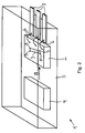
- An in Fig. 1 1 as a whole designated magnetic field sensor arrangement has a built-in semiconductor chip 2 magnetic field sensor 3, which is arranged in the magnetic field of a permanent magnetic magnetic field source 4.
- a field coil connected to a current source can also be provided.
- the semiconductor chip 2 and the magnetic field source 4 are embedded in an encapsulation material 5, for example in plastic.
- the semiconductor chip 2 has a plurality of connection points, which are each connected via a bonding wire 6 to an electrical connection contact 7.
- the connection contacts 7 each have a, the semiconductor chip 2 facing the first portion which is tightly encapsulated with the encapsulating material 5.
- a second section of the connection contact 7, which is spaced apart from the semiconductor chip 2, projects out of the encapsulation material 5 and can be connected to electrical lines.
- the magnetic field sensor 3 is designed as a Hall sensor, which has a Hall plate, which has two diametrically opposite one another in the plane of extension of the semiconductor chip 2 first terminals 8 for feeding a measuring current.
- the first terminals 8 are provided with an in Fig. 1 not shown, connected to the semiconductor chip 2 measuring current source connected.
- the Hall plate has two in the plane of extension of the semiconductor chip 2 diametrically opposed to each other second terminals 9, which are connected to a high-impedance, integrated in the semiconductor chip 2 measuring amplifier.
- Fig. 1 is clearly visible that the magnetic field source 4 is arranged in the plane of extension of the semiconductor chip 2 laterally next to this and spaced by the encapsulating material 5 of this. However, it is also conceivable that the semiconductor chip 2 laterally adjoins the magnetic field source 4 directly.
- the magnetic field source 4 is transverse and preferably magnetized normal to the extension plane of the semiconductor chip 2.
- a magnetic field sensor 3 a so-called horizontal Hall sensor is provided, whose Hall plate is arranged in the plane of extent of the semiconductor chip 2.
- the magnetic field source 4 is magnetized parallel to the plane of extension of the semiconductor chip 2.
- the direction of magnetization of the magnetic field source 4 extends approximately in the direction of a straight line connecting the magnetic field source 4 to the magnetic field sensor 3.
- the magnetization direction of the magnetic field source 4 in the plane of extent of the semiconductor chip 2 does not run on such a connecting line.
- a vertical Hall sensor is provided whose Hall plate is arranged approximately normal to the plane of extent of the semiconductor chip 2.
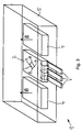
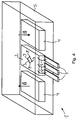
- two magnetic field sources 4 are arranged in the encapsulation material 5.
- the semiconductor chip 2 is positioned approximately centrally between these magnetic field sources 4. It can clearly be seen that the semiconductor chip 2 and the magnetic field sources 4 are arranged approximately in the same plane.
- the magnetization of the magnetic field sources 4 is oriented in the same direction and chosen such that the magnetic flux in the magnetic field sensor 3 is increased compared to a corresponding arrangement with only one magnetic field source 4.
- FIG. 5 In the embodiment shown, four magnetic field sources 4 are arranged in the encapsulation material 5 at equal intervals around the magnetic field sensor 3.
- the individual magnetic field sensors 3 are each offset by 90 ° to each other.
- the magnetic field sensors 3 and the Halbielterchip 2 are in turn arranged in the same plane.
- Adjacent magnetic field sources 4 may be magnetized in the same or opposite directions.
- the at least one permanent magnetic magnetic field source 4 is assigned a calibration coil 10 with which the magnetic flux in the magnetic field sensor 3 can be calibrated, for example to compensate for magnetic manufacturing tolerances of the magnetic field source (s) 4.
- the calibration coil 10 is connected to an adjustable current source, which is provided in a drive and / or evaluation device 11, which is shown only schematically in the drawing.
- the calibration coil 10 is integrated in the semiconductor chip 2 and has a plurality of mutually parallel first conductor tracks 12, which are arranged in a first conductor track plane.
- a plurality of mutually parallel second interconnects 13 are provided, which are connected via plated-through holes 14 with the first interconnects 12 in series.
- the windings of the calibration coil 10 bound the magnetic field sensor 3.
- the magnetic field generated by the calibration coil 10 extends approximately orthogonally to the plane of extent of the semiconductor chip 2.
- calibration coils 10 are also conceivable in which the coil turns are arranged in metallization planes of the semiconductor chip 2 in this way. the magnetic field extends in the plane of extent of the semiconductor chip 2 and / or parallel thereto.
- control and / or evaluation device 11 may have a mode switching device, by means of which the calibration coil 10 is selectively or alternately connectable to the current source or the measuring amplifier.
- the calibration coil 10 may then be connected to the sense amplifier to measure the voltage induced by the magnetic field in the calibration coil 10.
Landscapes
- Physics & Mathematics (AREA)
- General Physics & Mathematics (AREA)
- Condensed Matter Physics & Semiconductors (AREA)
- Measuring Magnetic Variables (AREA)
- Hall/Mr Elements (AREA)
Abstract
Description
- Die Erfindung betrifft eine Magnetfeldsensoranordnung mit mindestens einem, in einen Halbleiterchip Integrierten Magnetfeldsensor und mit wenigstens einer Magnetfeldquelle, wobei der Halbleiterchip und die wenigstens eine Magnetfeldquelle in einem Umkapselungsmaterial derart in einer vorbestimmten Lage relativ zueinander angeordnet sind, dass ein von der Magnetfeldquelle erzeugtes Magnetfeld mit Hilfe des mindestens einen Magnetfeldsensors detektierbar ist.
- Eine derartige Magnetfeldsensoranordnung ist aus
US 5 963 028 bekannt. Sie hat als Magnetfeldquelle einen als Stabmagnet ausgestalteten Permanentmagnet. Auf einer stirnseitigen Polfläche des Permanentmagnets ist ein flächiges metallisches Trägerplättchen angeordnet, dass mit einer seiner Unterseite flächig an der Polfläche des Permanentmagnets anliegt. Auf der Oberseite des Trägerplättchens ist ein Halbleiterchip etwa mittig zur der Polfläche angeordnet, der sich parallel zu dem Trägerplättchen und der Polfläche erstreckt und mit seiner Rückseite flächig an dem Trögerplättchen anliegt. In den Halbleiterchip ist als Magnetfeldsensor ein Hall-Sensor integriert. - An seiner dem Permanentmagnet abgewandten Vorderseite hat der Halbleiterchip drei elektrischen Anschlussstellen, die mit Bonddrähten verbunden sind. Ein erster Bonddraht ist an einer mit dem Trägerplättchen einstückig verbundenen ersten Kontaktfahne, ein zweiter Bonddraht an einer zweiten Kontaktfahne und ein dritter Bonddraht an einer dritten Kontaktfahne angeordnet. Der Permanentmagnet, das Trägerplättchen und der Halbleiterchip sind vollständig und die Kontaktfahnen teilweise mit einer elektrisch Isolierenden Vergussmasse umkapselt. Zum Verbinden mit externen elektrischen Leitern oder Anschlüssen ragen die Kontaktfahnen mit ihren von den Bonddrähten entfernten Endbereichen aus der Vergussmasse heraus.
- Der Magnetfeldsensoranordnung ist ein rotierendes Zahnrad zugeordnet, das aus einem weichmagnetischen Werkstoff besteht. Die Magnetfeldsensoranordnung ist am Außenumfang eines Zahnrads angeordnet und derart durch einen Luftspalt von dem Zahnrad beabstandet, dass der von dem Permanentmagnet erzeugte magnetische Fluss durch das Zahnrad hindurchfließt. Je nach dem, ob ein Zahn oder eine Zahnlücke an dem Hallsensor positioniert ist, ergibt sich in diesem ein unterschiedlicher magnetischer Fluss. Mit Hilfe der Magnetfeldsensoranordnung kann die Drehbewegung des Zahnrads detektiert werden.
- Da die Magnetfeldquelle bereits In die Magnetfeldsensoranordnung integriert ist, kann eine zusätzliche Magnetfeldquelle und somit ein entsprechender Montage- und Justieraufwand eingespart werden. Ungünstig ist jedoch, dass die Magnetfeldsensoranordnung relativ große Abmessungen aufweist. Daher ist sie beispielsweise für den Einbau in einen schmalen Spalt praktisch nicht geeignet.
- Es besteht deshalb die Aufgabe, eine Magnetfeldsensoranordnung der eingangs genannten Art zu schaffen, die eine flache Bauform ermöglicht.
- Erfindungsgemäß wird diese Aufgabe dadurch gelöst, dass die Magnetfeldquelle in dem Halbleiterchip und/oder in der Erstreckungsebene des Halbleiterchips seitlich neben diesem angeordnet ist.
- In vorteilhafter Weise ist es dadurch möglich, die Bauhöhe der Magnetfeldsensoranordnung auf die Bauhöhe eines entsprechenden Halbleiterbauelements, das keine Magnetfeldquelle beinhaltet, zu reduzieren. Dennoch können magnetisch leitfähige Werkstoffe, die in den Wirkungsbereich des von der Magnetfeldquelle erzeugten magnetischen Felds gelangen und dessen Flussdichte verändern, mit Hilfe des Magnetfeldsensors auf einfache Weise detektiert werden.
- Bei einer vorteilhaften Ausgestaltung der Erfindung weist die mindestens eine Magnetfeldquelle einen Permanentmagneten auf. Dadurch wird ein relativ großer magnetischer Fluss und somit eine hohe Messempfindlichkelt der Magnetfeldsensoranordnung ermöglicht.
- Bei einer anderen zweckmäßigen Ausführungsform der Erfindung weist die mindestens eine Magnetfeldquelle eine Feldspule auf, die mit einem Stromversorgungsanschluss verbunden ist. Der magnetische Fluss kann dann in Abhängigkeit von der jeweiligen Anwendung durch entsprechendes Bestromen der Feldspule eingestellt werden. Dabei ist es sogar möglich, dass die Feldspule zum Erzeugen eines magnetischen Wechselfelds mit einer Wechselstromquelle verbunden ist und dass als Magnetfeldsensor eine Messspule vorgesehen ist. Die Stromversorgung der Feldspule kann von einer in den Halbleiterchip integrierten Steuereinrichtung gesteuert sein.
- Bei einer Weiterbildung der Erfindung ist vorgesehen, dass mindestens zwei Magnetfeldquellen in dem Umkapselungsmaterial angeordnet sind, und dass der Halbleiterchip zwischen diesen Magnetfeldquellen vorgesehen ist. Dadurch ergibt sich ein symmetrischer Aufbau, der im Bereich des Magnetfeldsensors bei Annäherung der Magnetfeldsensoranordnung an einen ferromagnetischen Gegenstand und/oder beim Entfernen der Magnetfeldsensoranordnung von dem ferromagnetischen Gegenstand eine starke Veränderung des magnetischen Flusses und somit eine hohe Messempfindlichkeit ermöglicht.
- Vorteilhaft ist, wenn die Magnetfelder der mindestens zwei Magnetfeldquellen derart orientiert sind, dass sie sich an dem Magnetfeldsensor zumindest teilweise kompensieren. Dabei ist es sogar möglich, dass die Magnetisierungsrichtung von mindestens zwei Magnetfeldquellen in und/oder parallel zur Erstreckungsebene des Halbleiterchips angeordnet ist, und dass diese Magnetfeldquellen in entgegengesetzte Richtung magnetisiert sind, so dass der magnetische Fluss in dem Magnetfeldsensor etwa gleich Null ist, wenn kein magnetisch leitfähiger und/oder magnetischer Werkstoff im Wirkungsbereich der Magnetfeldquellen angeordnet ist. Das Messsignal des Magnetfeldsensors kann dann mittels eines Messverstärkers relativ stark verstärkt werden. Die Magnetfeldsensoranordnung reagiert dann noch empfindlicher auf Veränderungen der magnetischen Leitfähigkelt und/oder Fremdmagnetfelder in ihrer Umgebung.
- Bei einer bevorzugten Ausgestaltung der Erfindung ist dem mindestens einen Permanentmagnet wenigstens eine mit einer verstellbaren Stromquelle verbundene Kalibrierspule zum Kalibrieren des Magnetfelds zugeordnet, wobei der Magnetfeldsensor im magnetischen Wirkungsbereich der Kalibrierspule angeordnet ist. Mit Hilfe der wenigstens einen Kalibrierspule können dann Toleranzen in der Magnetisierung des Permanentmagnets kompensiert werden. Dabei ist es sogar denkbar, dass um den Magnetfeldsensor herum mehrere Kalibrierspulen, die jeweils mittels einer ihr zugeordneten Stromquelle ansteuerbar sind, angeordnet sind. Dabei sind die Kalibrierspulen vorzugsweise in unterschiedlichen Sektoren vorgesehen. Wenn aus unterschiedlichen Richtungen ein ferromagnetischer Körper an den Magnetfeldsensor angenähert wird, kann mit Hilfe der in den unterschiedlichen Sektoren befindlichen Kalibrierspulen eine vorbestimmte Detektionsempfindlichkeit erreicht werden, insbesondere eine symmetrische Detektionsempfindlichkeit. Die Magnetfeldsensoranordnung kann beispielsweise für absolute Abstandsmessungen verwendet werden.
- Vorteilhaft ist, wenn die Feldspule und/oder Kalibrierspule in den Halbleiterchip integriert ist. Die Magnetfeldsensoranordnung ermöglicht dann einen noch kompakteren und kostengünstigeren Aufbau. Die Feldspule kann Leiterbahnen aufweisen, die in zwei oder mehr Ebenen des Halbleiterchips angeordnet und über Durchkontaktierungen miteinander verbunden sind.
- Bei einer zweckmäßigen Ausführungsform der Erfindung sind mindestens vier Magnetfeldquellen in dem Umkapselungsmaterial um den Halbleiterchip herum angeordnet, vorzugsweise in gleichen Winkelabständen zueinander. Wenn die Magnetfelder der einzelnen Magnetfeldquellen in dieselbe Richtung orientiert sind, ergibt sich dann um den Magnetfeldsensor herum eine weitgehend symmetrische magnetische Flussdichte. Es ist aber auch denkbar, dass mindestens zwei Magnetfeldquellen in entgegengesetzte Richtungen magnetisiert sind, um entfang einer um den Magnetfeldsensor herumführenden Linie eine asymmetrische magnetische Flussdichte zu erreichen.
- Bei einer anderen Ausgestaltung der Erfindung umgrenzt die Magnetfeldquelle den mindestens einen Magnetfeldsensor ringförmig. Dadurch wird um den Magnetfeldsensor herum eine noch gleichmäßigere Verteilung der magnetischen Flussdichte ermöglicht.
- Die mindestens eine Magnetfeldquelle und/oder die Kalibrierspule kann (können) mit ihrer Magnetisierungsachse in und/oder parallel zu der Erstreckungsebene des Halbleiterchips angeordnet sein. Der Magnetfeldsensor weist dann bevorzugt parallel zur Magnetisierungsachse seine größte Messempfindlichkeit auf. Als Magnetfeldsensor ist dabei bevorzugt mindestens ein vertikaler Hallsensor vorgesehen. Es ist aber auch denkbar, dass der Magnetfeldsensor ein magnetoresistiver Sensor ist.
- Die mindestens eine Magnetfeldquelle und/oder die Kalibrierspule kann (können) mit ihrer Magnetisierungsachse auch orthogonal zur Erstreckungsebene des Halbleiterchips angeordnet sein. Dabei kann als Magnetfeldsensor ein horizontaler Hallsensor vorgesehen sein.
- Zweckmäßigerweise ist in den Halbleiterchip eine Ansteuerungs- und/oder Auswerteeinrichtung integriert, die zumindest einen mit dem mindestens einen Magnetfeldsensor verbunden Messsignaleingang aufweist. Die Auswerteeinrichtung kann eine Vergleichseinrichtung zum Vergleichen des Messsignals des mindestens einen Magnetfeldsensors mit einem Sollwert oder Sollwertbereich und/oder Filter zum Unterdrücken von Störsignalen aufweisen.
- Bei einer vorteilhaften Ausgestaltung der Erfindung ist mindestens eine Feldspule zum Erzeugen eines magnetischen Wechselfelds an einer Wechselstromquelle angeschlossen und die Ansteuerungs- und/oder Auswerteeinrichtung weist eine Korrelationseinrichtung auf, die einen ersten, mit dem mindestens einen Magnetfeldsensor verbundenen Eingang und einen zweiten, mit der Wechselstromquelle verbunden Eingang hat. Die Magnetfeldsensoranordnung ist dann gegen magnetische Störfelder weitgehend unempfindlich.
- Nachfolgend sind Ausführungsbeispiele der Erfindung anhand der Zeichnung näher erläutert. Es zeigt:
- Fig. 1 und 2
- eine Magnetfeldsensoranordnung, die in einem Umkapselungsma- terial einen in einen Halbleiterchip integrierten Magnetfeldsensor und eine Magnetfeldquelle aufweist,
- Fig. 3 und 4
- eine Magnetfeldsensoranordnung, bei dem im Umkapselungsmate- rial zwei Magnetfeldquellen vorgesehen sind, zwischen denen der Halbleiterchip angeordnet ist,
- Fig. 5
- eine Magnetfeldsensoranordnung, bei dem im Umkapselungsmate- rial vier Magnetfeldquellen um den Halbleiterchip herum angeord- net sind, und
- Fig. 6
- eine Aufsicht auf einen Halbleiterchip, in den ein Magnetfeldsensor, eine Kalibrierspule und eine Ansteuerungs- und Auswerteeinrichtung integriert sind, wobei im inneren des Halbleiterchips befindliche Lei- terbahnen strichliniert dargestellt sind.
- Eine in
Fig. 1 im Ganzen mit 1 bezeichnete Magnetfeldsensoranordnung weist einen in einen Halbleiterchip 2 integrierten Magnetfeldsensor 3 auf, der im Magnetfeld einer permanentmagnetischen Magnetfeldquelle 4 angeordnet ist. Anstelle der permanentmagnetischen Magnetfeldquelle 4 kann auch eine mit einer Stromquelle verbundene Feldspule vorgesehen sein. - Der Halbleiterchip 2 und die Magnetfeldquelle 4 sind In ein Umkapselungsmaterial 5 eingebettet, beispielsweise in Kunststoff. Der Halbleiterchip 2 hat mehrere Anschlussstellen, die jeweils über einen Bonddraht 6 mit einem elektrischen Anschlusskontakt 7 verbunden sind. Die Anschlusskontakte 7 haben jeweils einen, dem Halbleiterchip 2 zugewandten ersten Abschnitt, der mit dem Umkapselungsmaterial 5 dicht umspritzt ist. Ein von dem Halbleiterchip 2 beabstandeter zweiter Abschnitt des Anschlusskontakts 7 ragt aus dem Umkapselungsmaterial 5 heraus und kann mit elektrischen Leitungen verbunden werden.
- Der Magnetfeldsensor 3 ist als Hall-Sensor ausgestaltet, der eine Hall-Platte aufweist, die zwei in der Erstreckungsebene des Halbleiterchips 2 diametral einander gegenüberliegende erste Anschlüsse 8 zum Einspeisen eines Messstroms aufweist. Die ersten Anschlüsse 8 sind mit einer in
Fig. 1 nicht näher dargestellten, in den Halbleiterchip 2 integrierten Messstromquelle verbunden. - Außerdem hat die Hall-Platte zwei in der Erstreckungsebene des Halbleiterchips 2 diametral einander gegenüberliegende zweite Anschlüsse 9, die mit einem hochohmigen, in den Halbleiterchip 2 integrierten Meßverstärker verbunden sind.
- In
Fig. 1 ist deutlich erkennbar, dass die Magnetfeldquelle 4 in der Erstreckungsebene des Halbleiterchips 2 seitlich neben diesem angeordnet und durch das Umkapselungsmaterial 5 von diesem beabstandet ist. Es ist aber auch denkbar, dass der Halbleiterchips 2 seitlich direkt an die Magnetfeldquelle 4 angrenzt. - Bei dem in
Fig. 1 abgebildeten Ausführungsbelspiel ist die Magnetfeldquelle 4 quer und vorzugsweise normal zur Erstreckungsebene des Halbleiterchips 2 magnetisiert. Als Magnetfeldsensor 3 ist eine so genannter horizontaler Hall-Sensor vorgesehen, dessen Hall-Platte in der Erstreckungsebene des Halbleiterchips 2 angeordnet ist. - Bei dem in
Fig. 2 dargestellten Ausführungsbeispiel ist die Magnetfeldquelle 4 parallel zur Erstreckungsebene des Halbleiterchips 2 magnetisiert. Dabei verläuft die Magnetisierungsrichtung der Magnetfeldquelle 4 etwa in Richtung einer die Magnetfeldquelle 4 mit dem Magnetfeldsensor 3 verbindenden geraden Linie. Es sind aber auch andere Ausführungsformen denkbar, bei denen die Magnetisierungsrichtung der Magnetfeldquelle 4 in der Erstreckungsebene des Halbleiterchips 2 nicht auf einer solchen Verbindungslinle verläuft. Als Magnetfeldsensor 3 ist inFig. 2 ein vertikaler Hall-Sensor vorgesehen, dessen Hall-Platte etwa normal zur Erstreckungsebene des Halbleiterchips 2 angeordnet ist. - Bei den in
Fig. 3 und4 gezeigten Ausführungsbeispielen sind jeweils zwei Magnetfeldquellen 4 In dem Umkapselungsmaterial 5 angeordnet. Dabei ist der Halbleiterchip 2 etwa mittig zwischen diesen Magnetfeldquellen 4 positioniert. Deutlich ist erkennbar, dass der Halbleiterchip 2 und die Magnetfeldquellen 4 etwa in derselben Ebene angeordnet sind. - Bei dem Ausführungsbeispiel gemäß
Fig. 3 ist die Magnetisierung der Magnetfeldquellen 4 in dieselbe Richtung orientiert und derart gewählt, dass der magnetische Fluss in dem Magnetfeldsensor 3 gegenüber einer entsprechenden Anordnung mit nur einer Magnetfeldquellen 4 vergrößert ist. Wenn in die Nähe der Magnetfeldsensoranordnung 1 ein ferromagnetisch leitfähiger Körper gebracht wird, wird die Symmetrie des magnetischen Feldes gestört, so dass der Magnetfeldsensor 3 dann von einem magnetischen Fluss durchströmt wird. Das Messsignal des Magnetfeldsensors 3 verändert sich dann entsprechend. - Bei dem in
Fig. 4 gezeigten Ausführungsbelspiel sind die beiden beidseits des Magnetfeldsensors 3 angeordneten Magnetfeldquellen 4 derart in zueinander entgegengesetzte Richtung orientiert, dass der magnetische Fluss an dem Magnetfeldsensor 3 etwa gleich null ist, wenn in der Umgebung der Magnetfeldsensoranordnung 1 kein ferromagnetisch leitfähiges Material angeordnet ist. Wenn in die Umgebung der Magnetfeldsensoranordnung 1 ein ferromagnetisch leitfähiger Körper gebracht oder aus dieser entfernt wird, verändert sich die magnetische Flussdichte an dem Magnetfeldsensor 3. - Bei dem In
Fig. 5 gezeigten Ausführungsbeispiel sind vier Magnetfeldquellen 4 in dem Umkapselungsmaterlal 5 in gleichen Abständen um den Magnetfeldsensor 3 herum angeordnet. Dabei sind die einzelnen Magnetfeldsensoren 3 jeweils um 90° zueinander versetzt. Die Magnetfeldsensoren 3 und der Halbielterchip 2 sind wiederum in derselben Ebene angeordnet. Zueinander benachbarte Magnetfeldquellen 4 können in dieselbe oder in zueinander entgegengesetzte Richtungen magnetisiert sein. - Bei dem In
Fig. 6 gezeigten Ausführungsbeispiel ist der mindestens einen permanentmagnetischen Magnetfeldquelle 4 eine Kalibrierspule 10 zugeordnet, mit welcher der magnetische Fluss in dem Magnetfeldsensor 3 kalibrierbar ist, beispleisweise um magnetische Fertigungstoleranzen der Magnetfeldquelle(n) 4 auszugleichen. Die Kalibrierspule 10 ist mit einer verstellbaren Stromquelle verbunden, die in einer in der Zeichnung nur schematisch dargestellten Ansteuerungs- und/oder Auswerteeinrichtung 11 vorgesehen ist. Die Kalibrierspule 10 ist in den Halbleiterchip 2 integriert und weist mehrere parallel zueinander verlaufende erste Leiterbahnen 12 auf, die in einer ersten Leiterbahnebene angeordnet sind. In einer zweiten Leiterbahnebene sind mehrere parallel zueinander verlaufende zweite Leiterbahnen 13 vorgesehen, die über Durchkontaktierungen 14 mit den ersten Leiterbahnen 12 in Reihe geschaltet sind. Die Windungen der Kalibrierspule 10 umgrenzen den Magnetfeldsensor 3. - Bei dem in
Fig. 6 gezeigten Ausführungsbeispiel verläuft das von der Kalibrierspule 10 erzeugte Magnetfeld etwa orthogonal zur Erstreckungsebene des Halbleiterchips 2. Es sind aber auch Kalibrierspulen 10 denkbar, bei denen die Spulenwindungen derart in Metallisierungsebenen des Halbleiterchips 2 angeordnet sind, dass das Magnetfeld in der Erstreckungsebene des Halbleiterchips 2 und/oder parallel dazu verläuft. - Erwähnt werden soll noch, dass die Ansteuerungs- und/oder Auswerteeinrichtung 11 eine Betriebsartenumschalteinrichtung aufweisen kann, mittels der die Kalibrierspule 10 wahl- oder wechselweise mit der Stromquelle oder dem Messverstärker verbindbar ist. Bei Anwendungen, für die eine Kalibrierung des Magnetfelds nicht erforderlich ist, kann dann die Kalibrierspule 10 mit dem Messverstärker verbunden sein, um die durch das magnetische Feld in der Kalibrierspule 10 induzierte elektrische Spannung zu messen.
Claims (14)
- Magnetfeldsensoranordnung (1) mit mindestens einem, in einen Halbleiter-chip (2) integrierten Magnetfeldsensor (3) und mit wenigstens einer Magnetfeldquelle (4), wobei der Halbleiterchip (2) und die wenigstens eine Magnetfeldquelle (4) in einem Umkapselungsmaterial (5) derart in einer vorbestimmten Lage relativ zueinander angeordnet sind, dass ein von der Magnetfeldquelle (4) erzeugtes Magnetfeld mit Hilfe des mindestens einen Magnetfeldsensors (3) detektierbar ist, dadurch gekennzeichnet, dass die Magnetfeldquelle (4) in dem Halbleiterchip (2) und/oder in der Erstreckungsebene des Halbleiterchips (2) seitlich neben diesem angeordnet ist.
- Magnetfeldsensoranordnung (1) nach Anspruch 1, dadurch gekennzeichnet, dass die mindestens eine Magnetfeldquelle (4) einen Permanentmagneten aufweist.
- Magnetfeldsensoranordnung (1) nach Anspruch 1 oder 2, dadurch gekennzeichnet, dass die mindestens eine Magnetfeldquelle (4) eine Feldspule aufweist, die mit einem Stromversorgungsanschluss verbunden ist.
- Magnetfeldsensoranordnung (1) nach einem der Ansprüche 1 bis 3, dadurch gekennzeichnet, dass mindestens zwei Magnetfeldquellen (4) in dem Umkapselungsmaterial (5) angeordnet sind, und dass der Halbleiterchip (2) zwischen diesen Magnetfeldquellen (4) vorgesehen ist.
- Magnetfeldsensoranordnung (1) nach Anspruch 4, dadurch gekennzeichnet, dass die Magnetfelder der mindestens zwei Magnetfeldquellen (4) derart orientiert sind, dass sie sich an dem Magnetfeldsensor (3) zumindest teilweise kompensieren.
- Magnetfeldsensoranordnung (1) nach einem der Ansprüche 2 bis 5, dadurch gekennzeichnet, dass mindestens einem Permanentmagnet wenigstens eine mit einer verstellbaren Stromquelle verbundene Kalibrierspule (10) zum Kalibrieren des Magnetfelds zugeordnet ist, und dass der Magnetfeldsensor (3) im magnetischen Wirkungsbereich der Kalibrierspule (10) angeordnet ist.
- Magnetfeldsensoranordnung (1) nach einem der Ansprüche 3 bis 6, dadurch gekennzeichnet, dass die Feldspule und/oder die Kalibrierspule (10) in den Halbleiterchip (2) integriert ist.
- Magnetfeldsensoranordnung (1) nach einem der Ansprüche 1 bis 7, dadurch gekennzeichnet, dass mindestens vier Magnetfeldquellen (4) in dem Umkapselungsmaterial (5) um den Halbleiterchip (2) herum angeordnet sind, vorzugsweise in gleichen Winkelabständen zueinander.
- Magnetfeldsensoranordnung (1) nach einem der Ansprüche 1 bis 8, dadurch gekennzeichnet, dass die Magnetfeldquelle (4) den mindestens einen Magnetfeldsensor (3) ringförmig umgrenzt.
- Magnetfeldsensoranordnung (1) nach einem der Ansprüche 1 bis 9, dadurch gekennzeichnet, dass die mindestens eine Magnetfeldquelle (4) und/oder Kalibrierspule (10) mit ihrer Magnetisierungsachse in und/oder parallel zu der Erstreckungsebene des Halbleiterchips (2) angeordnet ist.
- Magnetfeldsensoranordnung (1) nach einem der Ansprüche 1 bis 10, dadurch gekennzeichnet, dass die mindestens eine Magnetfeldquelle (4) und/oder die Kalibrierspule (10) mit ihrer Magnetisierungsachse orthogonal zur Erstreckungsebene des Halbleiterchips (2) angeordnet ist.
- Magnetfeldsensoranordnung (1) nach einem der Ansprüche 1 bis 11, dadurch gekennzeichnet, dass mindestens ein Magnetfeldsensor (3) ein Hall-Sensor ist, vorzugsweise eine horizontaler Hallsensor und/oder ein vertikaler Hallsensor.
- Magnetfeldsensoranordnung (1) nach einem der Ansprüche 1 bis 12, dadurch gekennzeichnet, dass in den Halbleiterchip (2) eine Ansteuerungs- und/oder Auswerteeinrichtung (11) integriert ist, die zumindest einen mit dem mindestens einen Magnetfeldsensor (3) verbunden Messsignaleingang aufweist.
- Magnetfeldsensoranordnung (1) nach einem der Ansprüche 3 bis 13, dadurch gekennzeichnet, dass mindestens eine Feldspule zum Erzeugen eines magnetischen Wechselfelds an einer Wechselstromquelle angeschlossen ist und dass die Ansteuerungs- und/oder Auswerteeinrichtung (11) eine Korrelationseinrichtung aufweist, die einen ersten, mit dem mindestens einen Magnetfeldsensor (3) verbundenen Eingang und einen zweiten, mit der Wechselstromquelle verbunden Eingang aufweist.
Priority Applications (2)
| Application Number | Priority Date | Filing Date | Title |
|---|---|---|---|
| EP07022559A EP2063229B1 (de) | 2007-11-21 | 2007-11-21 | Magnetfeldsensoranordnung |
| US12/274,564 US8089276B2 (en) | 2007-11-21 | 2008-11-20 | Magnetic field sensor assembly |
Applications Claiming Priority (1)
| Application Number | Priority Date | Filing Date | Title |
|---|---|---|---|
| EP07022559A EP2063229B1 (de) | 2007-11-21 | 2007-11-21 | Magnetfeldsensoranordnung |
Publications (2)
| Publication Number | Publication Date |
|---|---|
| EP2063229A1 true EP2063229A1 (de) | 2009-05-27 |
| EP2063229B1 EP2063229B1 (de) | 2012-05-02 |
Family
ID=39870047
Family Applications (1)
| Application Number | Title | Priority Date | Filing Date |
|---|---|---|---|
| EP07022559A Ceased EP2063229B1 (de) | 2007-11-21 | 2007-11-21 | Magnetfeldsensoranordnung |
Country Status (2)
| Country | Link |
|---|---|
| US (1) | US8089276B2 (de) |
| EP (1) | EP2063229B1 (de) |
Cited By (32)
| Publication number | Priority date | Publication date | Assignee | Title |
|---|---|---|---|---|
| DE102010028390A1 (de) * | 2010-04-29 | 2011-11-03 | Fraunhofer-Gesellschaft zur Förderung der angewandten Forschung e.V. | Verfahren zur Bestimmung eines Erregerleiterabstandes von einem Magnetfeldsensor, Verfahren zum Kalibrieren des Magnetfeldsensors sowie ein kalibrierbarer Magnetfeldsensor und Verwendung einer Erregerleiterstruktur zur Bestimmung eines Erregerleiterabstandes |
| DE102010062237A1 (de) | 2010-12-01 | 2012-06-06 | Robert Bosch Gmbh | Verfahren zum Kalibrieren eines Magnetfeldsensors |
| WO2014149416A3 (en) * | 2013-03-15 | 2014-10-23 | Allegro Microsystems, Llc | Magnetic field sensor having an externally accessible coil |
| WO2015009423A1 (en) * | 2013-07-19 | 2015-01-22 | Allegro Microsystems, Llc | Arrangements for magnetic field sensors that act as tooth detectors |
| WO2015009442A1 (en) * | 2013-07-19 | 2015-01-22 | Allegro Microsystems, Llc | Methods and apparatus for magnetic sensor producing a changing magnetic field |
| US9719806B2 (en) | 2014-10-31 | 2017-08-01 | Allegro Microsystems, Llc | Magnetic field sensor for sensing a movement of a ferromagnetic target object |
| US9720054B2 (en) | 2014-10-31 | 2017-08-01 | Allegro Microsystems, Llc | Magnetic field sensor and electronic circuit that pass amplifier current through a magnetoresistance element |
| US9817078B2 (en) | 2012-05-10 | 2017-11-14 | Allegro Microsystems Llc | Methods and apparatus for magnetic sensor having integrated coil |
| US9823090B2 (en) | 2014-10-31 | 2017-11-21 | Allegro Microsystems, Llc | Magnetic field sensor for sensing a movement of a target object |
| US9823092B2 (en) | 2014-10-31 | 2017-11-21 | Allegro Microsystems, Llc | Magnetic field sensor providing a movement detector |
| US10012518B2 (en) | 2016-06-08 | 2018-07-03 | Allegro Microsystems, Llc | Magnetic field sensor for sensing a proximity of an object |
| US10041810B2 (en) | 2016-06-08 | 2018-08-07 | Allegro Microsystems, Llc | Arrangements for magnetic field sensors that act as movement detectors |
| US10260905B2 (en) | 2016-06-08 | 2019-04-16 | Allegro Microsystems, Llc | Arrangements for magnetic field sensors to cancel offset variations |
| US10310028B2 (en) | 2017-05-26 | 2019-06-04 | Allegro Microsystems, Llc | Coil actuated pressure sensor |
| US10324141B2 (en) | 2017-05-26 | 2019-06-18 | Allegro Microsystems, Llc | Packages for coil actuated position sensors |
| US10495699B2 (en) | 2013-07-19 | 2019-12-03 | Allegro Microsystems, Llc | Methods and apparatus for magnetic sensor having an integrated coil or magnet to detect a non-ferromagnetic target |
| US10641842B2 (en) | 2017-05-26 | 2020-05-05 | Allegro Microsystems, Llc | Targets for coil actuated position sensors |
| US10712403B2 (en) | 2014-10-31 | 2020-07-14 | Allegro Microsystems, Llc | Magnetic field sensor and electronic circuit that pass amplifier current through a magnetoresistance element |
| US10823586B2 (en) | 2018-12-26 | 2020-11-03 | Allegro Microsystems, Llc | Magnetic field sensor having unequally spaced magnetic field sensing elements |
| US10837943B2 (en) | 2017-05-26 | 2020-11-17 | Allegro Microsystems, Llc | Magnetic field sensor with error calculation |
| US10866117B2 (en) | 2018-03-01 | 2020-12-15 | Allegro Microsystems, Llc | Magnetic field influence during rotation movement of magnetic target |
| US10955306B2 (en) | 2019-04-22 | 2021-03-23 | Allegro Microsystems, Llc | Coil actuated pressure sensor and deformable substrate |
| US10996289B2 (en) | 2017-05-26 | 2021-05-04 | Allegro Microsystems, Llc | Coil actuated position sensor with reflected magnetic field |
| US11061084B2 (en) | 2019-03-07 | 2021-07-13 | Allegro Microsystems, Llc | Coil actuated pressure sensor and deflectable substrate |
| US11237020B2 (en) | 2019-11-14 | 2022-02-01 | Allegro Microsystems, Llc | Magnetic field sensor having two rows of magnetic field sensing elements for measuring an angle of rotation of a magnet |
| US11255700B2 (en) | 2018-08-06 | 2022-02-22 | Allegro Microsystems, Llc | Magnetic field sensor |
| US11262422B2 (en) | 2020-05-08 | 2022-03-01 | Allegro Microsystems, Llc | Stray-field-immune coil-activated position sensor |
| US11280637B2 (en) | 2019-11-14 | 2022-03-22 | Allegro Microsystems, Llc | High performance magnetic angle sensor |
| US11428755B2 (en) | 2017-05-26 | 2022-08-30 | Allegro Microsystems, Llc | Coil actuated sensor with sensitivity detection |
| US11493361B2 (en) | 2021-02-26 | 2022-11-08 | Allegro Microsystems, Llc | Stray field immune coil-activated sensor |
| US11578997B1 (en) | 2021-08-24 | 2023-02-14 | Allegro Microsystems, Llc | Angle sensor using eddy currents |
| US12523717B2 (en) | 2024-02-15 | 2026-01-13 | Allegro Microsystems, Llc | Closed loop magnetic field sensor with current control |
Families Citing this family (21)
| Publication number | Priority date | Publication date | Assignee | Title |
|---|---|---|---|---|
| US9476915B2 (en) * | 2010-12-09 | 2016-10-25 | Infineon Technologies Ag | Magnetic field current sensors |
| WO2013112214A2 (en) | 2011-10-18 | 2013-08-01 | California Institute Of Technology | Efficient active multi-drive radiator |
| US9201123B2 (en) * | 2011-11-04 | 2015-12-01 | Infineon Technologies Ag | Magnetic sensor device and a method for fabricating the same |
| US9121880B2 (en) * | 2011-11-04 | 2015-09-01 | Infineon Technologies Ag | Magnetic sensor device |
| US9921255B2 (en) | 2012-02-13 | 2018-03-20 | California Institute Of Technology | Sensing radiation metrics through mode-pickup sensors |
| US9686070B2 (en) | 2012-02-17 | 2017-06-20 | California Institute Of Technology | Dynamic polarization modulation and control |
| US20130335072A1 (en) * | 2012-06-15 | 2013-12-19 | Wolfram Malzfeldt | Steering torque angle sensor having a processor and a magneto-resistive element configured in a monolithic architecture |
| WO2014018927A1 (en) | 2012-07-26 | 2014-01-30 | California Institute Of Technology | Optically driven active radiator |
| CN103576101A (zh) * | 2012-07-31 | 2014-02-12 | 北京嘉岳同乐极电子有限公司 | 一种多通道集成式磁传感器 |
| JP6103640B2 (ja) * | 2013-07-16 | 2017-03-29 | アルプス電気株式会社 | 位置検出装置 |
| KR102030189B1 (ko) * | 2013-07-29 | 2019-11-11 | 매그나칩 반도체 유한회사 | 웨이퍼 상의 자기 센서 테스트 장치 및 방법 |
| US10589074B2 (en) | 2016-06-30 | 2020-03-17 | Integra Lifesciences Switzerland Sàrl | Magneto-resistive sensor tool set for hydrocephalus valve |
| US10286196B2 (en) | 2016-06-30 | 2019-05-14 | Integra Lifesciences Switzerland Sàrl | Device to control magnetic rotor of a programmable hydrocephalus valve |
| EP3467528B1 (de) | 2017-10-06 | 2020-05-20 | Melexis Technologies NV | Kalibrierung der empfindlichkeitsanpassung eines magnetsensors |
| US20210190893A1 (en) | 2017-10-06 | 2021-06-24 | Melexis Technologies Nv | Magnetic sensor sensitivity matching calibration |
| US20200309983A1 (en) | 2019-03-29 | 2020-10-01 | Ablic Inc. | Magnetic substance detection sensor |
| JP2020167370A (ja) | 2019-03-29 | 2020-10-08 | エイブリック株式会社 | 磁性体検出センサ |
| US11035910B2 (en) | 2019-03-29 | 2021-06-15 | Ablic Inc. | Magnetic substance detection sensor |
| JP2020165940A (ja) | 2019-03-29 | 2020-10-08 | エイブリック株式会社 | 磁性体検出センサ |
| JP2021047036A (ja) | 2019-09-17 | 2021-03-25 | エイブリック株式会社 | 磁性体検出センサ |
| US11604058B2 (en) | 2020-02-25 | 2023-03-14 | Allegro Microsystems, Llc | Reducing stray magnetic field effect on an angle sensor |
Citations (14)
| Publication number | Priority date | Publication date | Assignee | Title |
|---|---|---|---|---|
| US4772929A (en) * | 1987-01-09 | 1988-09-20 | Sprague Electric Company | Hall sensor with integrated pole pieces |
| DE4200466A1 (de) * | 1991-01-14 | 1992-07-16 | Gen Motors Corp | Pack fuer auf magnetfeld ansprechendes bauelement |
| EP0537419A1 (de) * | 1991-10-09 | 1993-04-21 | Landis & Gyr Business Support AG | Anordnung mit einem integrierten Magnetfeldsensor sowie einem ferromagnetischen ersten und zweiten Magnetfluss-Konzentrator und Verfahren zum Einbau einer Vielzahl von Anordnungen in je einem Kunststoffgehäuse |
| EP0544479A2 (de) * | 1991-11-26 | 1993-06-02 | Honeywell Inc. | Magnetfeldfühler |
| EP0680103A1 (de) * | 1994-04-25 | 1995-11-02 | General Motors Corporation | Sensor für magnetische Felder |
| DE19620548A1 (de) * | 1995-05-31 | 1996-12-05 | Allegro Microsystems Inc | Magnetfeld-Sensoranordnung |
| US5631557A (en) * | 1996-02-16 | 1997-05-20 | Honeywell Inc. | Magnetic sensor with encapsulated magnetically sensitive component and magnet |
| US5637995A (en) * | 1992-12-09 | 1997-06-10 | Nippondenso Co., Ltd. | Magnetic detection device having a magnet including a stepped portion for eliminating turbulence at the MR sensor |
| US5883567A (en) * | 1997-10-10 | 1999-03-16 | Analog Devices, Inc. | Packaged integrated circuit with magnetic flux concentrator |
| US5912556A (en) * | 1996-11-06 | 1999-06-15 | Honeywell Inc. | Magnetic sensor with a chip attached to a lead assembly within a cavity at the sensor's sensing face |
| US5963028A (en) | 1997-08-19 | 1999-10-05 | Allegro Microsystems, Inc. | Package for a magnetic field sensing device |
| US20040095129A1 (en) * | 2002-11-15 | 2004-05-20 | Furlong Gregory R. | Sensing methods and systems for hall and/or mr sensors |
| FR2852098A1 (fr) * | 2003-03-03 | 2004-09-10 | Denso Corp | Capteur magentique et procede pour fabriquer ce dernier |
| WO2006106454A1 (en) * | 2005-04-08 | 2006-10-12 | Koninklijke Philips Electronics N.V. | A device with a sensor arrangement |
Family Cites Families (2)
| Publication number | Priority date | Publication date | Assignee | Title |
|---|---|---|---|---|
| US6989642B2 (en) * | 2003-10-16 | 2006-01-24 | Invacare Corporation | Method and apparatus for embedding motor error parameter data in a drive motor of a power driven wheelchair |
| WO2009047585A1 (en) * | 2007-10-09 | 2009-04-16 | Nds Limited | Tamper-detecting electronic system |
-
2007
- 2007-11-21 EP EP07022559A patent/EP2063229B1/de not_active Ceased
-
2008
- 2008-11-20 US US12/274,564 patent/US8089276B2/en active Active
Patent Citations (14)
| Publication number | Priority date | Publication date | Assignee | Title |
|---|---|---|---|---|
| US4772929A (en) * | 1987-01-09 | 1988-09-20 | Sprague Electric Company | Hall sensor with integrated pole pieces |
| DE4200466A1 (de) * | 1991-01-14 | 1992-07-16 | Gen Motors Corp | Pack fuer auf magnetfeld ansprechendes bauelement |
| EP0537419A1 (de) * | 1991-10-09 | 1993-04-21 | Landis & Gyr Business Support AG | Anordnung mit einem integrierten Magnetfeldsensor sowie einem ferromagnetischen ersten und zweiten Magnetfluss-Konzentrator und Verfahren zum Einbau einer Vielzahl von Anordnungen in je einem Kunststoffgehäuse |
| EP0544479A2 (de) * | 1991-11-26 | 1993-06-02 | Honeywell Inc. | Magnetfeldfühler |
| US5637995A (en) * | 1992-12-09 | 1997-06-10 | Nippondenso Co., Ltd. | Magnetic detection device having a magnet including a stepped portion for eliminating turbulence at the MR sensor |
| EP0680103A1 (de) * | 1994-04-25 | 1995-11-02 | General Motors Corporation | Sensor für magnetische Felder |
| DE19620548A1 (de) * | 1995-05-31 | 1996-12-05 | Allegro Microsystems Inc | Magnetfeld-Sensoranordnung |
| US5631557A (en) * | 1996-02-16 | 1997-05-20 | Honeywell Inc. | Magnetic sensor with encapsulated magnetically sensitive component and magnet |
| US5912556A (en) * | 1996-11-06 | 1999-06-15 | Honeywell Inc. | Magnetic sensor with a chip attached to a lead assembly within a cavity at the sensor's sensing face |
| US5963028A (en) | 1997-08-19 | 1999-10-05 | Allegro Microsystems, Inc. | Package for a magnetic field sensing device |
| US5883567A (en) * | 1997-10-10 | 1999-03-16 | Analog Devices, Inc. | Packaged integrated circuit with magnetic flux concentrator |
| US20040095129A1 (en) * | 2002-11-15 | 2004-05-20 | Furlong Gregory R. | Sensing methods and systems for hall and/or mr sensors |
| FR2852098A1 (fr) * | 2003-03-03 | 2004-09-10 | Denso Corp | Capteur magentique et procede pour fabriquer ce dernier |
| WO2006106454A1 (en) * | 2005-04-08 | 2006-10-12 | Koninklijke Philips Electronics N.V. | A device with a sensor arrangement |
Non-Patent Citations (10)
| Title |
|---|
| AHN C H ET AL: "A fully integrated micromagnetic actuator with a multilevel meander magnetic core", SOLID-STATE SENSOR AND ACTUATOR WORKSHOP, 1992. 5TH TECHNICAL DIGEST., IEEE HILTON HEAD ISLAND, SC, USA 22-25 JUNE 1992, NEW YORK, NY, USA,IEEE, US, 22 June 1992 (1992-06-22), pages 14 - 18, XP010056347, ISBN: 978-0-7803-0456-7 * |
| BALTES H: "Future of IC microtransducers", SENSORS AND ACTUATORS A, ELSEVIER SEQUOIA S.A., LAUSANNE, CH, vol. 56, no. 1, 1 August 1996 (1996-08-01), pages 179 - 192, XP004013031, ISSN: 0924-4247 * |
| DANIEL J SADLER ET AL: "MICROMACHINED SEMI-ENCAPSULAED SPIRAL INDUCTORS FOR MICRO ELECTRO MECHANICAL SYSTEMS (MEMS) APPLICATIONS", IEEE TRANSACTIONS ON MAGNETICS, IEEE SERVICE CENTER, NEW YORK, NY, US, vol. 33, no. 5, 1 September 1997 (1997-09-01), pages 3319 - 3321, XP011086140, ISSN: 0018-9464 * |
| DAUGHTON J: "Spin-dependent sensors", PROCEEDINGS OF THE IEEE, IEEE. NEW YORK, US, vol. 91, no. 5, 1 May 2003 (2003-05-01), pages 681 - 686, XP011096630, ISSN: 0018-9219 * |
| DRAXELMAYR D ET AL: "A Chopped Hall Sensor With Small Jitter and Programmable True Power-On Function", IEEE JOURNAL OF SOLID-STATE CIRCUITS, IEEE SERVICE CENTER, PISCATAWAY, NJ, US, vol. 40, no. 7, 1 July 2005 (2005-07-01), pages 1533 - 1540, XP011135461, ISSN: 0018-9200 * |
| ESASHI M ET AL: "Packaged micromechanical sensors", EMERGING TECHNOLOGIES AND FACTORY AUTOMATION, 1994. ETFA '94., IEEE SY MPOSIUM ON TOKYO, JAPAN 6-10 NOV. 1994, NEW YORK, NY, USA,IEEE, 6 November 1994 (1994-11-06), pages 30 - 37, XP010139977, ISBN: 978-0-7803-2114-4 * |
| HSING-CHENG CHANG ET AL: "A Novel Electro-Optical Magnetic Microsensor with Reducing Interference Packaging", ELECTRONIC PACKAGING TECHNOLOGY, 2007. ICEPT 2007. 8TH INTERNATIONAL C ONFERENCE ON, IEEE, PI, 1 August 2007 (2007-08-01), pages 1 - 4, XP031209975, ISBN: 978-1-4244-1391-1 * |
| JAMES M DAUGHTON: "GMR and SDT Sensor Applications", IEEE TRANSACTIONS ON MAGNETICS, IEEE SERVICE CENTER, NEW YORK, NY, US, vol. 36, no. 5, 1 September 2000 (2000-09-01), XP011032900, ISSN: 0018-9464 * |
| LENZ J E ET AL: "A high-sensitivity magnetoresistive sensor", 19900604; 19900604 - 19900607, 4 June 1990 (1990-06-04), pages 114 - 117, XP010000748 * |
| POPOVIC ET AL: "CMOS magnetic sensors with integrated ferromagnetic parts", SENSORS AND ACTUATORS A, ELSEVIER SEQUOIA S.A., LAUSANNE, CH, vol. 129, no. 1-2, 24 May 2006 (2006-05-24), pages 94 - 99, XP005427207, ISSN: 0924-4247 * |
Cited By (55)
| Publication number | Priority date | Publication date | Assignee | Title |
|---|---|---|---|---|
| DE102010028390B4 (de) * | 2010-04-29 | 2012-12-06 | Fraunhofer-Gesellschaft zur Förderung der angewandten Forschung e.V. | Verfahren zur Bestimmung eines Erregerleiterabstandes von einem Magnetfeldsensor, Verfahren zum Kalibrieren des Magnetfeldsensors sowie ein kalibrierbarer Magnetfeldsensor und Verwendung einer Erregerleiterstruktur zur Bestimmung eines Erregerleiterabstandes |
| EP2564225A1 (de) * | 2010-04-29 | 2013-03-06 | Fraunhofer Gesellschaft zur Förderung der angewandten Wissenschaft E.V. | Verfahren zur bestimmung eines erregerleiterabstandes, verfahren zum kalibrieren eines magnetfeldsensors, kalibrierbarer magnetfeldsensor und verwendung einer erregerleiterstruktur zur bestimmung eines erregerleiterabstandes zwischen einem erregerleiter und einem magnetfeldsensor |
| DE102010028390A1 (de) * | 2010-04-29 | 2011-11-03 | Fraunhofer-Gesellschaft zur Förderung der angewandten Forschung e.V. | Verfahren zur Bestimmung eines Erregerleiterabstandes von einem Magnetfeldsensor, Verfahren zum Kalibrieren des Magnetfeldsensors sowie ein kalibrierbarer Magnetfeldsensor und Verwendung einer Erregerleiterstruktur zur Bestimmung eines Erregerleiterabstandes |
| US9000754B2 (en) | 2010-04-29 | 2015-04-07 | Fraunhofer-Gesellschaft Zur Foerderung Der Angewandten Forschung E.V. | Method for determining an exciter conductor spacing from a magnetic field sensor, method for calibrating the magnetic field sensor as well as calibratable magnetic field sensor and usage of an exciter conductor structure for determining an exciter conductor spacing |
| DE102010062237A1 (de) | 2010-12-01 | 2012-06-06 | Robert Bosch Gmbh | Verfahren zum Kalibrieren eines Magnetfeldsensors |
| US11680996B2 (en) | 2012-05-10 | 2023-06-20 | Allegro Microsystems, Llc | Methods and apparatus for magnetic sensor having integrated coil |
| US9817078B2 (en) | 2012-05-10 | 2017-11-14 | Allegro Microsystems Llc | Methods and apparatus for magnetic sensor having integrated coil |
| WO2014149416A3 (en) * | 2013-03-15 | 2014-10-23 | Allegro Microsystems, Llc | Magnetic field sensor having an externally accessible coil |
| US10725100B2 (en) | 2013-03-15 | 2020-07-28 | Allegro Microsystems, Llc | Methods and apparatus for magnetic sensor having an externally accessible coil |
| WO2015009423A1 (en) * | 2013-07-19 | 2015-01-22 | Allegro Microsystems, Llc | Arrangements for magnetic field sensors that act as tooth detectors |
| US12061246B2 (en) | 2013-07-19 | 2024-08-13 | Allegro Microsystems, Llc | Method and apparatus for magnetic sensor producing a changing magnetic field |
| EP3168634A1 (de) | 2013-07-19 | 2017-05-17 | Allegro Microsystems, LLC | Anordnungen für magnetfeldsensoren als zahndetektoren |
| US9810519B2 (en) | 2013-07-19 | 2017-11-07 | Allegro Microsystems, Llc | Arrangements for magnetic field sensors that act as tooth detectors |
| CN105378500A (zh) * | 2013-07-19 | 2016-03-02 | 阿莱戈微系统有限责任公司 | 用于产生变化的磁场的磁传感器的方法和装置 |
| US11313924B2 (en) | 2013-07-19 | 2022-04-26 | Allegro Microsystems, Llc | Method and apparatus for magnetic sensor producing a changing magnetic field |
| WO2015009442A1 (en) * | 2013-07-19 | 2015-01-22 | Allegro Microsystems, Llc | Methods and apparatus for magnetic sensor producing a changing magnetic field |
| US10495699B2 (en) | 2013-07-19 | 2019-12-03 | Allegro Microsystems, Llc | Methods and apparatus for magnetic sensor having an integrated coil or magnet to detect a non-ferromagnetic target |
| US10670672B2 (en) | 2013-07-19 | 2020-06-02 | Allegro Microsystems, Llc | Method and apparatus for magnetic sensor producing a changing magnetic field |
| US10145908B2 (en) | 2013-07-19 | 2018-12-04 | Allegro Microsystems, Llc | Method and apparatus for magnetic sensor producing a changing magnetic field |
| US10254103B2 (en) | 2013-07-19 | 2019-04-09 | Allegro Microsystems, Llc | Arrangements for magnetic field sensors that act as tooth detectors |
| US10712403B2 (en) | 2014-10-31 | 2020-07-14 | Allegro Microsystems, Llc | Magnetic field sensor and electronic circuit that pass amplifier current through a magnetoresistance element |
| US9823090B2 (en) | 2014-10-31 | 2017-11-21 | Allegro Microsystems, Llc | Magnetic field sensor for sensing a movement of a target object |
| US9719806B2 (en) | 2014-10-31 | 2017-08-01 | Allegro Microsystems, Llc | Magnetic field sensor for sensing a movement of a ferromagnetic target object |
| US9720054B2 (en) | 2014-10-31 | 2017-08-01 | Allegro Microsystems, Llc | Magnetic field sensor and electronic circuit that pass amplifier current through a magnetoresistance element |
| US11307054B2 (en) | 2014-10-31 | 2022-04-19 | Allegro Microsystems, Llc | Magnetic field sensor providing a movement detector |
| US10753768B2 (en) | 2014-10-31 | 2020-08-25 | Allegro Microsystems, Llc | Magnetic field sensor providing a movement detector |
| US10753769B2 (en) | 2014-10-31 | 2020-08-25 | Allegro Microsystems, Llc | Magnetic field sensor providing a movement detector |
| US9823092B2 (en) | 2014-10-31 | 2017-11-21 | Allegro Microsystems, Llc | Magnetic field sensor providing a movement detector |
| US10260905B2 (en) | 2016-06-08 | 2019-04-16 | Allegro Microsystems, Llc | Arrangements for magnetic field sensors to cancel offset variations |
| US10837800B2 (en) | 2016-06-08 | 2020-11-17 | Allegro Microsystems, Llc | Arrangements for magnetic field sensors that act as movement detectors |
| US10041810B2 (en) | 2016-06-08 | 2018-08-07 | Allegro Microsystems, Llc | Arrangements for magnetic field sensors that act as movement detectors |
| US10012518B2 (en) | 2016-06-08 | 2018-07-03 | Allegro Microsystems, Llc | Magnetic field sensor for sensing a proximity of an object |
| US11320496B2 (en) | 2017-05-26 | 2022-05-03 | Allegro Microsystems, Llc | Targets for coil actuated position sensors |
| US10837943B2 (en) | 2017-05-26 | 2020-11-17 | Allegro Microsystems, Llc | Magnetic field sensor with error calculation |
| US10996289B2 (en) | 2017-05-26 | 2021-05-04 | Allegro Microsystems, Llc | Coil actuated position sensor with reflected magnetic field |
| US10324141B2 (en) | 2017-05-26 | 2019-06-18 | Allegro Microsystems, Llc | Packages for coil actuated position sensors |
| US10649042B2 (en) | 2017-05-26 | 2020-05-12 | Allegro Microsystems, Llc | Packages for coil actuated position sensors |
| US10641842B2 (en) | 2017-05-26 | 2020-05-05 | Allegro Microsystems, Llc | Targets for coil actuated position sensors |
| US11073573B2 (en) | 2017-05-26 | 2021-07-27 | Allegro Microsystems, Llc | Packages for coil actuated position sensors |
| US11428755B2 (en) | 2017-05-26 | 2022-08-30 | Allegro Microsystems, Llc | Coil actuated sensor with sensitivity detection |
| US11768256B2 (en) | 2017-05-26 | 2023-09-26 | Allegro Microsystems, Llc | Coil actuated sensor with sensitivity detection |
| US10310028B2 (en) | 2017-05-26 | 2019-06-04 | Allegro Microsystems, Llc | Coil actuated pressure sensor |
| US10866117B2 (en) | 2018-03-01 | 2020-12-15 | Allegro Microsystems, Llc | Magnetic field influence during rotation movement of magnetic target |
| US11313700B2 (en) | 2018-03-01 | 2022-04-26 | Allegro Microsystems, Llc | Magnetic field influence during rotation movement of magnetic target |
| US11255700B2 (en) | 2018-08-06 | 2022-02-22 | Allegro Microsystems, Llc | Magnetic field sensor |
| US11686599B2 (en) | 2018-08-06 | 2023-06-27 | Allegro Microsystems, Llc | Magnetic field sensor |
| US10823586B2 (en) | 2018-12-26 | 2020-11-03 | Allegro Microsystems, Llc | Magnetic field sensor having unequally spaced magnetic field sensing elements |
| US11061084B2 (en) | 2019-03-07 | 2021-07-13 | Allegro Microsystems, Llc | Coil actuated pressure sensor and deflectable substrate |
| US10955306B2 (en) | 2019-04-22 | 2021-03-23 | Allegro Microsystems, Llc | Coil actuated pressure sensor and deformable substrate |
| US11280637B2 (en) | 2019-11-14 | 2022-03-22 | Allegro Microsystems, Llc | High performance magnetic angle sensor |
| US11237020B2 (en) | 2019-11-14 | 2022-02-01 | Allegro Microsystems, Llc | Magnetic field sensor having two rows of magnetic field sensing elements for measuring an angle of rotation of a magnet |
| US11262422B2 (en) | 2020-05-08 | 2022-03-01 | Allegro Microsystems, Llc | Stray-field-immune coil-activated position sensor |
| US11493361B2 (en) | 2021-02-26 | 2022-11-08 | Allegro Microsystems, Llc | Stray field immune coil-activated sensor |
| US11578997B1 (en) | 2021-08-24 | 2023-02-14 | Allegro Microsystems, Llc | Angle sensor using eddy currents |
| US12523717B2 (en) | 2024-02-15 | 2026-01-13 | Allegro Microsystems, Llc | Closed loop magnetic field sensor with current control |
Also Published As
| Publication number | Publication date |
|---|---|
| EP2063229B1 (de) | 2012-05-02 |
| US20090140724A1 (en) | 2009-06-04 |
| US8089276B2 (en) | 2012-01-03 |
Similar Documents
| Publication | Publication Date | Title |
|---|---|---|
| EP2063229B1 (de) | Magnetfeldsensoranordnung | |
| DE10150955C1 (de) | Vertikaler Hall-Sensor | |
| EP2867684B1 (de) | Anordnung zur strommessung | |
| EP0226574B1 (de) | Magnetoresistiver sensor zur abgabe von elektrischen signalen | |
| DE102016103325B4 (de) | Magnetischer Winkelpositionssensor | |
| EP2553400B1 (de) | Magnetischer drehgeber | |
| EP2037286A1 (de) | Messvorrichtung zur Messung eines magnetischen Felds | |
| EP0807256A1 (de) | Einrichtung zur drehzahlmessung oder drehrichtungserkennung eines drehmagnetfeldes | |
| DE3908892A1 (de) | Schaltungsanordnung und vorrichtung zur kontaktlosen sollwertvorgabe fuer einen mit nichtmagnetischem werkstoff umhuellten integrierten schaltkreis | |
| DE112012006270T5 (de) | Magnetpositions-Erfassungsvorrichtung | |
| EP2470920A1 (de) | Magnetfeldsensor | |
| DE102022106330A1 (de) | Magnetsensorsystem | |
| EP3936828A1 (de) | Gebersystem für einen antrieb | |
| WO2009015496A1 (de) | Elektromotor mit rotorpositionssensoranordnung | |
| WO2007135006A1 (de) | Planarer direktantrieb und dazugehöriger sensoreinheit | |
| DE19612422C2 (de) | Potentiometereinrichtung mit einem linear verschiebbaren Stellelement und signalerzeugenden Mitteln | |
| DE102006024722A1 (de) | Magnetfelddetektor sowie Verfahren zu seiner Herstellung | |
| DE102010036040A1 (de) | Strommesseinrichtung, insbesondere in einem Umrichter eines Flurförderzeugs | |
| EP2149784A1 (de) | Magnetisches Wegsensorsystem | |
| EP2100102B1 (de) | Messanordnung | |
| DE102020132914A1 (de) | Initialisierungsvorrichtung | |
| DE102011086034A1 (de) | Halbleitervorrichtung | |
| DE102010050356B4 (de) | Magnetfeldsensor | |
| EP0797078A1 (de) | Induktiver Drehwinkelsensor | |
| DE102020119985A1 (de) | Positionssensor zum Bestimmen der Position einer Ventilstange eines Stellventils |
Legal Events
| Date | Code | Title | Description |
|---|---|---|---|
| PUAI | Public reference made under article 153(3) epc to a published international application that has entered the european phase |
Free format text: ORIGINAL CODE: 0009012 |
|
| AK | Designated contracting states |
Kind code of ref document: A1 Designated state(s): AT BE BG CH CY CZ DE DK EE ES FI FR GB GR HU IE IS IT LI LT LU LV MC MT NL PL PT RO SE SI SK TR |
|
| AX | Request for extension of the european patent |
Extension state: AL BA HR MK RS |
|
| 17P | Request for examination filed |
Effective date: 20091114 |
|
| AKX | Designation fees paid |
Designated state(s): DE FR GB |
|
| 17Q | First examination report despatched |
Effective date: 20110124 |
|
| GRAP | Despatch of communication of intention to grant a patent |
Free format text: ORIGINAL CODE: EPIDOSNIGR1 |
|
| GRAS | Grant fee paid |
Free format text: ORIGINAL CODE: EPIDOSNIGR3 |
|
| GRAA | (expected) grant |
Free format text: ORIGINAL CODE: 0009210 |
|
| AK | Designated contracting states |
Kind code of ref document: B1 Designated state(s): DE FR GB |
|
| REG | Reference to a national code |
Ref country code: GB Ref legal event code: FG4D Free format text: NOT ENGLISH |
|
| REG | Reference to a national code |
Ref country code: DE Ref legal event code: R096 Ref document number: 502007009804 Country of ref document: DE Effective date: 20120705 |
|
| PLBE | No opposition filed within time limit |
Free format text: ORIGINAL CODE: 0009261 |
|
| STAA | Information on the status of an ep patent application or granted ep patent |
Free format text: STATUS: NO OPPOSITION FILED WITHIN TIME LIMIT |
|
| 26N | No opposition filed |
Effective date: 20130205 |
|
| REG | Reference to a national code |
Ref country code: DE Ref legal event code: R097 Ref document number: 502007009804 Country of ref document: DE Effective date: 20130205 |
|
| REG | Reference to a national code |
Ref country code: FR Ref legal event code: PLFP Year of fee payment: 9 |
|
| REG | Reference to a national code |
Ref country code: FR Ref legal event code: PLFP Year of fee payment: 10 |
|
| REG | Reference to a national code |
Ref country code: DE Ref legal event code: R082 Ref document number: 502007009804 Country of ref document: DE Representative=s name: KOCH-MUELLER PATENTANWALTSGESELLSCHAFT MBH, DE Ref country code: DE Ref legal event code: R081 Ref document number: 502007009804 Country of ref document: DE Owner name: TDK-MICRONAS GMBH, DE Free format text: FORMER OWNER: MICRONAS GMBH, 79108 FREIBURG, DE |
|
| REG | Reference to a national code |
Ref country code: FR Ref legal event code: PLFP Year of fee payment: 11 |
|
| REG | Reference to a national code |
Ref country code: FR Ref legal event code: CD Owner name: TDK-MICRONAS GMBH, DE Effective date: 20180717 |
|
| PGFP | Annual fee paid to national office [announced via postgrant information from national office to epo] |
Ref country code: GB Payment date: 20181120 Year of fee payment: 12 Ref country code: FR Payment date: 20181123 Year of fee payment: 12 |
|
| GBPC | Gb: european patent ceased through non-payment of renewal fee |
Effective date: 20191121 |
|
| PG25 | Lapsed in a contracting state [announced via postgrant information from national office to epo] |
Ref country code: GB Free format text: LAPSE BECAUSE OF NON-PAYMENT OF DUE FEES Effective date: 20191121 Ref country code: FR Free format text: LAPSE BECAUSE OF NON-PAYMENT OF DUE FEES Effective date: 20191130 |
|
| PGFP | Annual fee paid to national office [announced via postgrant information from national office to epo] |
Ref country code: DE Payment date: 20211118 Year of fee payment: 15 |
|
| REG | Reference to a national code |
Ref country code: DE Ref legal event code: R119 Ref document number: 502007009804 Country of ref document: DE |
|
| PG25 | Lapsed in a contracting state [announced via postgrant information from national office to epo] |
Ref country code: DE Free format text: LAPSE BECAUSE OF NON-PAYMENT OF DUE FEES Effective date: 20230601 |