EP2058860A2 - Zur zweiseitigen Kühlung konfiguriertes, vollständig prüfbares, oberflächenmontiertes Formgehäuse - Google Patents
Zur zweiseitigen Kühlung konfiguriertes, vollständig prüfbares, oberflächenmontiertes Formgehäuse Download PDFInfo
- Publication number
- EP2058860A2 EP2058860A2 EP08167416A EP08167416A EP2058860A2 EP 2058860 A2 EP2058860 A2 EP 2058860A2 EP 08167416 A EP08167416 A EP 08167416A EP 08167416 A EP08167416 A EP 08167416A EP 2058860 A2 EP2058860 A2 EP 2058860A2
- Authority
- EP
- European Patent Office
- Prior art keywords
- die
- laminate structure
- inboard
- conductor
- face
- Prior art date
- Legal status (The legal status is an assumption and is not a legal conclusion. Google has not performed a legal analysis and makes no representation as to the accuracy of the status listed.)
- Withdrawn
Links
Images

Classifications
-
- H—ELECTRICITY
- H01—ELECTRIC ELEMENTS
- H01L—SEMICONDUCTOR DEVICES NOT COVERED BY CLASS H10
- H01L23/00—Details of semiconductor or other solid state devices
- H01L23/52—Arrangements for conducting electric current within the device in operation from one component to another, i.e. interconnections, e.g. wires, lead frames
- H01L23/538—Arrangements for conducting electric current within the device in operation from one component to another, i.e. interconnections, e.g. wires, lead frames the interconnection structure between a plurality of semiconductor chips being formed on, or in, insulating substrates
- H01L23/5389—Arrangements for conducting electric current within the device in operation from one component to another, i.e. interconnections, e.g. wires, lead frames the interconnection structure between a plurality of semiconductor chips being formed on, or in, insulating substrates the chips being integrally enclosed by the interconnect and support structures
-
- H—ELECTRICITY
- H01—ELECTRIC ELEMENTS
- H01L—SEMICONDUCTOR DEVICES NOT COVERED BY CLASS H10
- H01L23/00—Details of semiconductor or other solid state devices
- H01L23/48—Arrangements for conducting electric current to or from the solid state body in operation, e.g. leads, terminal arrangements ; Selection of materials therefor
- H01L23/488—Arrangements for conducting electric current to or from the solid state body in operation, e.g. leads, terminal arrangements ; Selection of materials therefor consisting of soldered or bonded constructions
- H01L23/498—Leads, i.e. metallisations or lead-frames on insulating substrates, e.g. chip carriers
- H01L23/49833—Leads, i.e. metallisations or lead-frames on insulating substrates, e.g. chip carriers the chip support structure consisting of a plurality of insulating substrates
-
- H—ELECTRICITY
- H01—ELECTRIC ELEMENTS
- H01L—SEMICONDUCTOR DEVICES NOT COVERED BY CLASS H10
- H01L24/00—Arrangements for connecting or disconnecting semiconductor or solid-state bodies; Methods or apparatus related thereto
- H01L24/01—Means for bonding being attached to, or being formed on, the surface to be connected, e.g. chip-to-package, die-attach, "first-level" interconnects; Manufacturing methods related thereto
- H01L24/26—Layer connectors, e.g. plate connectors, solder or adhesive layers; Manufacturing methods related thereto
- H01L24/31—Structure, shape, material or disposition of the layer connectors after the connecting process
- H01L24/33—Structure, shape, material or disposition of the layer connectors after the connecting process of a plurality of layer connectors
-
- H—ELECTRICITY
- H01—ELECTRIC ELEMENTS
- H01L—SEMICONDUCTOR DEVICES NOT COVERED BY CLASS H10
- H01L2924/00—Indexing scheme for arrangements or methods for connecting or disconnecting semiconductor or solid-state bodies as covered by H01L24/00
- H01L2924/10—Details of semiconductor or other solid state devices to be connected
- H01L2924/11—Device type
- H01L2924/13—Discrete devices, e.g. 3 terminal devices
- H01L2924/1304—Transistor
- H01L2924/1306—Field-effect transistor [FET]
-
- H—ELECTRICITY
- H01—ELECTRIC ELEMENTS
- H01L—SEMICONDUCTOR DEVICES NOT COVERED BY CLASS H10
- H01L2924/00—Indexing scheme for arrangements or methods for connecting or disconnecting semiconductor or solid-state bodies as covered by H01L24/00
- H01L2924/15—Details of package parts other than the semiconductor or other solid state devices to be connected
- H01L2924/181—Encapsulation
Definitions
- the present invention relates to a surface mount electronic component including a power semiconductor die that is testable at full power and configured for both top-side and bottom-side cooling.
- High power transistor and diode semiconductor die configured for direct mounting on a substrate typically include terminal pads on both major faces.
- a power field effect transistor FET
- FET field effect transistor
- the terminals on one face of the die interface directly with conductors formed on the surface of a substrate on which the die is mounted, and the terminal(s) on the exposed face of the die can be coupled to other substrate conductors by wire bonding.
- the wire bonds interfere with top-side cooling of the die, effectively limiting the power dissipation of the device.
- the U.S. Patent No. 6,873,043 discloses an improved arrangement in which a heat conducting laminate structure couples terminal(s) on the exposed face of the die to substrate conductors and at the same time thermally couples the die to a top-side heatsink for improved heat dissipation.
- the present invention is directed to an improved packaging arrangement for a power semiconductor die in which the die is sandwiched between upper and lower heat conducting laminate structures to form a surface mount component that is configured for double-sided cooling.
- the upper heat conducting laminate structure electrically couples top-side die terminal(s) to conductors formed on the inboard face of the lower heat conducting laminate structure, and all of the die terminals are electrically coupled to conductors formed on the outboard face of the lower heat conducting laminate structure.
- the die package can be placed in a test fixture for full power testing since the upper and lower heat conducting laminate structures both protect the die and thermally couple it to the test fixture.
- the die package is installed in an electronic assembly including a substrate and upper and lower heatsinks, the die is thermally coupled to the upper heatsink through the upper heat conducting laminate structure, and to the lower heatsink through the substrate and the lower heat conducting laminate structure.
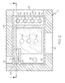
- FIG. 1 is a partial cross-sectional view of an electronic assembly including a substrate, upper and lower heatsinks, and a die package according to the present invention.
- FIG. 2 is a cross-sectional view of the electronic assembly of FIG. 1 taken along lines 2-2 of FIG. 1 .
- the reference numeral 10 generally designates an electronic assembly including an upper heatsink 12, a surface mount power transistor die package 14, a circuit board 16, and a lower heatsink 18.
- a conductor layer 20 formed on the upper face of die package 14 is thermally coupled to upper heatsink 12 with a thermal interface material 22, and set of die package terminals 24, 26, 28 formed on the lower face of die package 14 are soldered a set of conductors 30, 32, 34 formed on the upper face of circuit board 16.
- Conductor layers 36, 38 formed on the lower face of circuit board 16 are thermally coupled to lower heatsink 18 with a thermal interface material 40, and a set of metal-filled vias 42 thermally couple the upper conductor 32 to the lower conductor layer 36.
- the die package 14 is a surface-mount component that is manufactured, tested, and then mounted on the circuit board 16 as described above.
- the die package 14 includes a power FET die 50 sandwiched between an upper and lower heat conducting laminate structures 52 and 54, and a suitable under-fill material 55.
- the die package terminals 24, 26 and 28 are formed on the outboard face of lower heat conducting laminate structure 54, and are internally coupled to the gate, source and drain terminals 56, 58 and 60 of FET die 50. Since the upper and lower heat conducting laminate structures 52 and 54 are also thermally coupled to FET die 50, the die package 14 can be placed in a test fixture and tested at full power prior to its incorporation into the electronic assembly 10 of FIG. 1 .
- upper and lower heat conducting laminate structures 52, 54 each include a heat conductive but electrically insulative substrate 62, 64 of ceramic (SiN or AIN, for example) or organic material, and sets of metal (Cu or Ag, for example) conductors bonded to their upper and lower faces.
- the upper heat conductive laminate structure 52 includes the conductor layer 20 formed on the upper or outboard face of substrate 62, and a drain conductor 66 formed on the lower or inboard face of substrate 62.
- the drain conductor 66 is soldered to the drain terminal 60 of FET die 50, and the substrate 62 electrically isolates conductor layer 20 (and therefore heatsink 12) from the FET die 50.
- the lower heat conductive laminate structure 54 includes the die package terminals 24, 26 and 28 formed on the lower or outboard face of substrate 64, and gate, source and drain conductors 68, 70 and 72 formed on the upper or inboard face of substrate 64.
- the gate conductor 68 is thermally and electrically coupled to the die package terminal 24 by a metal filled via 74 through substrate 64;
- the source conductor 70 is thermally and electrically coupled to the die package terminal 26 by a set of three metal filled vias 76 through substrate 64;
- the drain conductor 72 is thermally and electrically coupled to the die package terminal 28 by a set of three metal filled vias 78 through substrate 64.
- the circuit board 16 electrically isolates the die package terminals 24 and 28 (i.e., the FET gate and drain) from heatsink 18; and the metal filled vias 42 and circuit board conductors 32 and 36 thermally couple the die package terminal 26 (i.e., the FET source) to heatsink 18.
- the upper and lower heat conducting laminate structures 52 and 54 are joined by a set of conductive standoffs 80-90 distributed about the lateral periphery of FET die 50.
- the standoffs 80-90 are integral with conductors formed on the inboard face of the upper heat conducting laminate structure 52, and are soldered to conductors formed on the inboard face of lower heat conducting laminate structure 54, but the opposite configuration is also possible.
- the standoffs 80-90 may be constructed, for example, by brazing copper balls onto a copper conductor, but other techniques are also possible.
- standoffs 80, 82, 84 and 86 extend between the drain conductor 66 of upper heat conducting laminate structure 52 and the drain conductor 72 of lower heat conducting laminate structure 54, and serve (along with vias 78) to electrically couple the FET drain terminal 60 to the die package terminal 28.
- the remaining standoffs 88 and 90 provide mechanical support between the heat conducting laminate structures 52 and 54, but serve no electrical function.
- the standoff 88 extends between the gate conductor 68 of lower heat conducting laminate structure 54 and a conductor 92 formed on the inboard face of upper substrate 62.
- the standoff 90 extends between the source conductor 70 of lower heat conducting laminate structure 54 and a conductor (not shown) formed on the inboard face of upper substrate 62.
- the above-described die package 14 and electronic assembly 10 offer many operating advantages, the foremost of which are significantly improve heat dissipation and full power testability. While the invention has been described with respect to the illustrated embodiment, it is recognized that numerous modifications and variations in addition to those mentioned herein will occur to those skilled in the art.
- the die 50 may be a device other than a FET, more or fewer standoffs may be used, the under-fill material 55 may be eliminated or replaced with a plastic molding compound, and so forth. Accordingly, it is intended that the invention not be limited to the disclosed embodiment, but that it have the full scope permitted by the language of the following claims.
Applications Claiming Priority (1)
| Application Number | Priority Date | Filing Date | Title |
|---|---|---|---|
| US11/983,247 US7564128B2 (en) | 2007-11-08 | 2007-11-08 | Fully testable surface mount die package configured for two-sided cooling |
Publications (2)
| Publication Number | Publication Date |
|---|---|
| EP2058860A2 true EP2058860A2 (de) | 2009-05-13 |
| EP2058860A3 EP2058860A3 (de) | 2011-03-23 |
Family
ID=40380070
Family Applications (1)
| Application Number | Title | Priority Date | Filing Date |
|---|---|---|---|
| EP08167416A Withdrawn EP2058860A3 (de) | 2007-11-08 | 2008-10-23 | Zur zweiseitigen Kühlung konfiguriertes, vollständig prüfbares, oberflächenmontiertes Formgehäuse |
Country Status (2)
| Country | Link |
|---|---|
| US (1) | US7564128B2 (de) |
| EP (1) | EP2058860A3 (de) |
Cited By (2)
| Publication number | Priority date | Publication date | Assignee | Title |
|---|---|---|---|---|
| AT514085A4 (de) * | 2013-06-11 | 2014-10-15 | Austria Tech & System Tech | Leistungsmodul |
| CN110326105A (zh) * | 2016-12-12 | 2019-10-11 | 维迪科研究所 | 用于集成功率芯片的方法和电子功率模块 |
Families Citing this family (3)
| Publication number | Priority date | Publication date | Assignee | Title |
|---|---|---|---|---|
| CN101568247B (zh) * | 2008-04-25 | 2012-09-05 | 深圳迈瑞生物医疗电子股份有限公司 | 屏蔽绝缘散热系统 |
| CN107429976B (zh) | 2015-03-16 | 2021-02-09 | 达纳加拿大公司 | 带有具有用于提高平坦度的表面图案的板的换热器和制造该换热器的方法 |
| KR101905995B1 (ko) | 2016-11-09 | 2018-10-10 | 현대자동차주식회사 | 양면냉각형 파워모듈 |
Citations (1)
| Publication number | Priority date | Publication date | Assignee | Title |
|---|---|---|---|---|
| US6873043B2 (en) | 2003-03-10 | 2005-03-29 | Delphi Technologies, Inc. | Electronic assembly having electrically-isolated heat-conductive structure |
Family Cites Families (2)
| Publication number | Priority date | Publication date | Assignee | Title |
|---|---|---|---|---|
| US6180881B1 (en) * | 1998-05-05 | 2001-01-30 | Harlan Ruben Isaak | Chip stack and method of making same |
| US7030317B1 (en) | 2005-04-13 | 2006-04-18 | Delphi Technologies, Inc. | Electronic assembly with stacked integrated circuit die |
-
2007
- 2007-11-08 US US11/983,247 patent/US7564128B2/en active Active
-
2008
- 2008-10-23 EP EP08167416A patent/EP2058860A3/de not_active Withdrawn
Patent Citations (1)
| Publication number | Priority date | Publication date | Assignee | Title |
|---|---|---|---|---|
| US6873043B2 (en) | 2003-03-10 | 2005-03-29 | Delphi Technologies, Inc. | Electronic assembly having electrically-isolated heat-conductive structure |
Cited By (3)
| Publication number | Priority date | Publication date | Assignee | Title |
|---|---|---|---|---|
| AT514085A4 (de) * | 2013-06-11 | 2014-10-15 | Austria Tech & System Tech | Leistungsmodul |
| AT514085B1 (de) * | 2013-06-11 | 2014-10-15 | Austria Tech & System Tech | Leistungsmodul |
| CN110326105A (zh) * | 2016-12-12 | 2019-10-11 | 维迪科研究所 | 用于集成功率芯片的方法和电子功率模块 |
Also Published As
| Publication number | Publication date |
|---|---|
| EP2058860A3 (de) | 2011-03-23 |
| US20090121340A1 (en) | 2009-05-14 |
| US7564128B2 (en) | 2009-07-21 |
Similar Documents
| Publication | Publication Date | Title |
|---|---|---|
| US7656015B2 (en) | Packaging substrate having heat-dissipating structure | |
| US6677672B2 (en) | Structure and method of forming a multiple leadframe semiconductor device | |
| EP1796163B1 (de) | Halbleiterbauelement und elektronische Steuerungseinheit unter Verwendung desselben | |
| US8451621B2 (en) | Semiconductor component and method of manufacture | |
| US7872869B2 (en) | Electronic chip module | |
| US9202798B2 (en) | Power module package and method for manufacturing the same | |
| US8916958B2 (en) | Semiconductor package with multiple chips and substrate in metal cap | |
| US10490473B2 (en) | Chip package module and circuit board structure comprising the same | |
| US20150359107A1 (en) | Electronic module with a plastic-coated electronic circuit and method for the production thereof | |
| US6809416B1 (en) | Package for integrated circuit with thermal vias and method thereof | |
| EP3310140B1 (de) | Montageanordnung mit einem kühlkörper | |
| KR20090056594A (ko) | 온도 감지소자가 장착된 반도체 파워 모듈 패키지 및 그제조방법 | |
| CN103703549A (zh) | 用于直接表面安装的裸露芯片封装 | |
| US7564128B2 (en) | Fully testable surface mount die package configured for two-sided cooling | |
| KR101008772B1 (ko) | 집적 회로 장치, 전자 회로 지지 기판 및 집적 회로와 히트싱크의 열적 접속 방법 | |
| US9659906B2 (en) | Semiconductor device | |
| KR101343199B1 (ko) | 반도체 패키지 | |
| US20060043550A1 (en) | Hermetic semiconductor package | |
| KR20060105403A (ko) | 혼성회로와 복합기판을 가지는 패키지 구조물 | |
| US6483706B2 (en) | Heat dissipation for electronic components | |
| US7310224B2 (en) | Electronic apparatus with thermal module | |
| KR20140002348A (ko) | 반도체 패키지 및 반도체 패키지 제조 방법 | |
| JP2011146513A (ja) | 半導体装置 | |
| JP5358515B2 (ja) | 半導体装置及びそれを用いた電子制御装置 | |
| US20050167696A1 (en) | Silicon nitride insulating substrate for power semiconductor module |
Legal Events
| Date | Code | Title | Description |
|---|---|---|---|
| PUAI | Public reference made under article 153(3) epc to a published international application that has entered the european phase |
Free format text: ORIGINAL CODE: 0009012 |
|
| AK | Designated contracting states |
Kind code of ref document: A2 Designated state(s): AT BE BG CH CY CZ DE DK EE ES FI FR GB GR HR HU IE IS IT LI LT LU LV MC MT NL NO PL PT RO SE SI SK TR |
|
| AX | Request for extension of the european patent |
Extension state: AL BA MK RS |
|
| PUAL | Search report despatched |
Free format text: ORIGINAL CODE: 0009013 |
|
| AK | Designated contracting states |
Kind code of ref document: A3 Designated state(s): AT BE BG CH CY CZ DE DK EE ES FI FR GB GR HR HU IE IS IT LI LT LU LV MC MT NL NO PL PT RO SE SI SK TR |
|
| AX | Request for extension of the european patent |
Extension state: AL BA MK RS |
|
| AKY | No designation fees paid | ||
| REG | Reference to a national code |
Ref country code: DE Ref legal event code: R108 |
|
| REG | Reference to a national code |
Ref country code: DE Ref legal event code: R108 Effective date: 20111130 |
|
| STAA | Information on the status of an ep patent application or granted ep patent |
Free format text: STATUS: THE APPLICATION IS DEEMED TO BE WITHDRAWN |
|
| 18D | Application deemed to be withdrawn |
Effective date: 20110924 |