EP2058820A1 - Semiconductor memory having segmented row repair - Google Patents
Semiconductor memory having segmented row repair Download PDFInfo
- Publication number
- EP2058820A1 EP2058820A1 EP09001943A EP09001943A EP2058820A1 EP 2058820 A1 EP2058820 A1 EP 2058820A1 EP 09001943 A EP09001943 A EP 09001943A EP 09001943 A EP09001943 A EP 09001943A EP 2058820 A1 EP2058820 A1 EP 2058820A1
- Authority
- EP
- European Patent Office
- Prior art keywords
- row
- redundant
- primary
- wordline
- memory
- Prior art date
- Legal status (The legal status is an assumption and is not a legal conclusion. Google has not performed a legal analysis and makes no representation as to the accuracy of the status listed.)
- Withdrawn
Links
Images




Classifications
-
- G—PHYSICS
- G11—INFORMATION STORAGE
- G11C—STATIC STORES
- G11C29/00—Checking stores for correct operation ; Subsequent repair; Testing stores during standby or offline operation
- G11C29/70—Masking faults in memories by using spares or by reconfiguring
- G11C29/78—Masking faults in memories by using spares or by reconfiguring using programmable devices
- G11C29/80—Masking faults in memories by using spares or by reconfiguring using programmable devices with improved layout
-
- G—PHYSICS
- G11—INFORMATION STORAGE
- G11C—STATIC STORES
- G11C29/00—Checking stores for correct operation ; Subsequent repair; Testing stores during standby or offline operation
Definitions
- a memory cell is accessed by applying a specific row address to the wordline drivers 34.
- a local wordline driver is driven by application of the address and a phase term provided from a global wordline driver (not shown) to activate the selected cell row via one of the row lines, while a column decoder (not shown) will activate the column select circuits to access specified memory cells on an open row. Accordingly, the selected row will be activated across all eight vertical strips 26a-26h.
- a compare circuit (not shown) compares each incoming address to the blown fuse addresses stored in the fuse banks to determine whether the incoming address matches with one of the blown fuse addresses. If the compare circuit determines a match, then it outputs a match signal (typically one bit). In response thereto, the wordline drivers 34 of a redundant row will be activated to access the redundant row in substitution for the row with the defective memory cell.
- Fig. 4 illustrates a portion of a memory device having segmented row repair in accordance with the present invention. Specifically, Fig. 4 illustrates the area between two vertical strips of the 256K blocks 30 where the wordline drivers 34 are located.
- the wordline drivers 34 for the segment of the row that includes a defective memory cell can be disabled, and one of the redundant wordline drivers 34 enabled, to replace the defective memory cell, as will be described further below.
- a global wordline driver 52 activates a desired row by providing an address term and four phase signals, as is known in the art.
- the four phase signals are global phase signal (GPH) ⁇ 0 > 60, GPH ⁇ 1 > 62, GPH ⁇ 2 > 64 and GPH ⁇ 3 > 66. Similar phase signals are also provided to activate the redundant row included in each 256K block 30.
- the signals for the redundant rows include redundant phase signal (RPH) ⁇ 0 > 70, RPH ⁇ 1 > 72, RPH ⁇ 2 > 74 and RPH ⁇ 3 > 76.
- RPH redundant phase signal
- a plurality of AND gates 50a-50h are provided. A first input of each AND gate 50a-50d is connected to one of the four global phase (GPH) signals 60-66 from the global driver 52, and a first input of each AND gate 50e-50h is connected to one of the four redundant phase (RPH) signals 70-76.
- AND gate 50a has a first input connected to the signal GPH ⁇ 1 > 62
- AND gate 50b has a first input connected to the signal GPH ⁇ 0 > 60
- AND gate 50c has a first input connected to the signal GPH ⁇ 3 > 66
- AND gate 50d has a first input connected to the signal GPH ⁇ 2 > 64
- AND gate 50e has a first input connected to the signal RPH ⁇ 1 > 72
- AND gate 50f has a first input connected to the signal RPH ⁇ 0 > 70
- AND gate 50g has a first input connected to the signal RPH ⁇ 3 > 76
- AND gate 50h has a first input connected to the signal RPH ⁇ 2 > 74.
- each AND gate 50a-50d is connected to the wordline drivers 34 for the primary rows of 256K blocks 30, while the output from each AND gate 50e-50h is connected to a redundant wordline drive 34 for the redundant rows of 256K blocks 30.
- the output from the AND gates 50a-50h in conjunction with the address terms from global driver 52 on bus line 80, will drive the desired wordline driver 34 or redundant wordline driver 34 to activate a selected primary row (labeled WL ⁇ 0 : 256 > ) or a redundant row (labeled RVVL ⁇ 0 : 1 > and RWL ⁇ 2 : 3 > ) in the 256K blocks 30.
- matching circuit 82 determines there is not a match, i. e., the address for the desired memory cell does not match the address of a defective memory cell, it is not necessary to substitute one of the redundant wordlines and the appropriate primary wordline can be activated.
- the redundant match signal RED 58 output from matching circuit 82 will be low, and accordingly signal RED* 56 will be high.
- the low input of signal RED 58 to AND gates 50e-50h will cause a low output from AND gates 50e-50h, regardless of the state of the RPH signals 70-76 being input to AND gates 50e-50h.
- the low outputs from AND gates 50e-50h will effectively disable the redundant wordline drivers 34 by not driving the redundant wordline, drivers 34.
- the high signal RED* 56 output from matching circuit 82 being input to the second input of AND gates 50a-50d will cause the output of one of the AND gates 50a-50d to be high, depending on the state of the GPH signals 60-66.
- Global driver 52 will output a high signal on one phase of signals GPH 60-66, and a high signal on the corresponding signal RPH 70-76, depending on the address of the memory cell selected for access and an address specified by match circuit 82 via line 83, respectively, and a low signal on the other three global and other three redundant phase signals.
- phase ⁇ 1 > For example, if the address of the cell for access requires that phase ⁇ 1 > be high, then both GPH ⁇ 1 > 62 and, for example, RPH ⁇ 1 > 72 will be high, while the remaining phase signals will be low. It should be noted, however, that any one of the redundant phase signals RPH 70-76 could be high depending on which programmed fuse bank matched the incoming address.
- the high signal GPH ⁇ 1 > 62 and the high signal RED* 56 input to AND gate 50a will cause a high output from AND gate 50a, which, along with the address term on bus line 80, will activate the appropriate wordline driver 34 to drive its associated wordline of a primary row of the 256K blocks 30 associated with that wordline driver 34.
- matching circuit 82 determines the address of the cell to be accessed matches a defective address, requiring substitution of a redundant element.
- Matching circuit 82 will output a high match signal RED 58 and accordingly signal RED* 56 will be low.
- the low input of signal RED* 56 to AND gates 50a-50d will cause a low output from AND gates 50a-50d, regardless of the state of the GPH signals 60-66 being input to AND gates 50a-50d.
- the low outputs from AND gates 50a-50d will effectively disable the wordline drivers 34 for the primary rows of the 256K blocks 30.
- the high signal RED 58 output from matching circuit 82 being input to the second input of AND gates 50e-50h will cause the output of one of the AND gates 50e-50h to be high, depending on the state of the RPH signals 70-76.
- global driver 52 will output a high signal on one phase of signals GPH 60-66, and a high signal on the corresponding signal RPH 70-76, depending on the address of the memory cell selected for access and an address specified by match circuit 82 via line 83, respectively, and a low signal on the other three global and other three redundant phase signals.
- phase ⁇ 1 > For example, if the address of the cell for access requires that phase ⁇ 1 > be high, then both GPH ⁇ 1 > 62 and, for example, RPH ⁇ 1 > 72 will be high, while the remaining phase signals will be low. It should be noted, however, that any one of the redundant phase signals RPH 70-76 could be high depending on which programmed fuse bank matched the incoming address.
- the high signal RPH ⁇ 1 > 72 and the high signal RED 58 input to AND gate 50e will cause a high output from AND gate 50e, which, along with the address term on line 80, will activate tulle appropriate redundant wordline driver 34 to drive its associated redundant wordline of a redundant row of its associated 256K blocks 30, such as for example RWL ⁇ 0 >
- Logic 84 selectively controls the application of the match signals RED 58 and RED* 56 to the vertical strip 26a-26h based on the address of the cell being accessed.
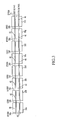
- each row across a bank of memory is segmented into four segments, labeled Segment ⁇ 0 > to Segment ⁇ 3 > .
- Segment ⁇ 0 > includes the 256K blocks 30 DQ ⁇ 0 > and DQ ⁇ 1 >
- Segment ⁇ 1 > includes the 256K blocks 30 DQ ⁇ 2 > and DQ ⁇ 3 >
- Segment ⁇ 2 > includes the 256K blocks 30 DQ ⁇ 4 > and DQ ⁇ 5 >
- Segment ⁇ 3 > includes the 256K blocks 30 DQ ⁇ 6 > and DQ ⁇ 7 >.
Landscapes
- For Increasing The Reliability Of Semiconductor Memories (AREA)
- Dram (AREA)
- Techniques For Improving Reliability Of Storages (AREA)
- Read Only Memory (AREA)
Abstract
Description
- The present invention relates generally to integrated circuit memory devices, and more particularly to a memory device having segmented row repair.
- Memory tests on semiconductor devices, such as random access memory (RAM) integrated circuits, e. g., DRAMs, SRAMs and the like, are typically performed by the manufacturer during production and fabrication to locate defects and failures in such devices that can occur during the manufacturing process of the semiconductor devices. Defects may be caused by a number of factors, including particle defects such as broken or shorted out columns and rows, particle contamination, or bit defects. The testing is typically performed by a memory controller or processor (or a designated processor in a multi-processor machine) which runs a testing program, often before a die containing the semiconductor device is packaged into a chip.
- Random access memories are usually subjected to data retention tests and/or data march tests. In data retention tests, every cell of the memory is written and checked after a pre-specified interval to determine if leakage current has occurred that has affected the stored logic state. In a march test, a sequence of read and/or write operations is applied to each cell, either in increasing or decreasing address order. Such testing ensures that hidden defects will not be first discovered during operational use, thereby rendering end-products unreliable.
- Many semiconductor devices, particularly memory devices, include redundant circuitry on the semiconductor device that can be employed to replace malfunctioning circuits found during testing. During the initial testing of a memory device, defective elements are repaired by replacing them with non-defective elements referred to as redundant elements. By enabling such redundant circuitry, the device need not be discarded even if it fails a particular test.
-
Fig. 1 illustrates in block diagram form a256Mbit DRAM 20.DRAM 20 includes eight memory banks orarrays 22a-22h, labeled BANI ( < 0 > to BANK < 7 > . Eachmemory bank 22a-h is a32Mbit array map 24 as illustrated inFig. 2 . The architecture ofarray map 24 illustrated inFig. 2 dividesarray map 24 into a plurality of 256K blocks 30 (only one labeled for clarity). As shown,array map 24 includes eightvertical strips 26a-26h of the256K blocks 30 across, labeled DQ < 0 > to DQ < 7 > and is sixteen strips of the256K blocks 30 high. Memory cells (not shown) in each256K block 30 are arranged in a plurality of primary rows and redundant rows. For example, typically 512 primary rows and 4 redundant rows are provided.Sense amplifiers 32 are provided between each row of256K blocks 30 for sensing a data stored in the memory cells therein. Wordlinedrivers 34 are provided on each side of each vertical strip of256IL blocks 30 for firing a wordline in each256K block 30 associated with a specified row address. Accordingly, there will be an associated wordline and wordline driver for each row of memory cells in a256K block 30. Thus, it should be understood thatwordline driver 34 actually comprises a plurality of wordline drivers, one for each wordline. - Within each
256K block 30, the rows are designated as either an even row or an odd row. Accordingly, eachwordline driver 34 will fire either a wordline associated with an odd row or an even row.Fig. 3 illustrates a single horizontal strip of256K blocks 30 fromFig. 2 . Wordlinedrivers drivers driver 34a will fire evenrows 40 inblock 26a, wordlinedriver 34c will fire evenrows 40 inblocks driver 34e will fire evenrows 40 inblocks driver 34g will fire evenrows 40 inblocks driver 34i will fire evenrows 40 inblock 26h. Conversely, wordlinedriver 34b will fireodd rows 42 inblocks driver 34d will fireodd rows 42 inblocks driver 34f will fireodd rows 42 inblocks driver 34h will fireodd rows 42 inblocks - A memory cell is accessed by applying a specific row address to the
wordline drivers 34. A local wordline driver is driven by application of the address and a phase term provided from a global wordline driver (not shown) to activate the selected cell row via one of the row lines, while a column decoder (not shown) will activate the column select circuits to access specified memory cells on an open row. Accordingly, the selected row will be activated across all eightvertical strips 26a-26h. - As noted above, memory devices typically employ redundant rows and columns of memory cells so that if a memory cell in a column or row of the primary memory array is defective, then an entire column or row of redundant memory cells can be substituted therefore. Substitution of one or more of the spare rows or columns is conventionally accomplished by opening a specific combination of fuses (not shown) or closing antifuses in one of several fuse banks (not shown) on the die. A selected combination of fuses are blown to provide an address equal to the address of the defective cell. For example, if the defective cell has an eight-bit binary address of 11011011, then the third and sixth fuses in a set of eight fuses within one of several fuse banks will be blown, thereby storing this address. A compare circuit (not shown) compares each incoming address to the blown fuse addresses stored in the fuse banks to determine whether the incoming address matches with one of the blown fuse addresses. If the compare circuit determines a match, then it outputs a match signal (typically one bit). In response thereto, the
wordline drivers 34 of a redundant row will be activated to access the redundant row in substitution for the row with the defective memory cell. - There are drawbacks, however, with the redundant row substitution approach described above. The redundant rows of memory cells necessarily occupy space on the die. Therefore, it is desirable to obtain the maximum number of repairs using a mmimum number of spare rows by utilizing a single bit repair method. This is not possible, however, when a complete redundant row must be substituted for a primary row that has only a single defective memory cell, as a substantial amount of nondefective memory cells will also necessarily be replaced by the redundant row. For example, if
vertical strip 26d ofFig. 3 has a defective memory cell, when a redundant row is used to replace the row in which the defective memory cell is located, the entire redundant row will be utilized across allstrips 26a-26h, even though there may be no defects in the corresponding row in the other sevenstrips 26a-26c and 26e-26h. - Thus, there exists a need for a memory device in which efficient use of a redundant circuit to replace a defective primary circuit is provided, thereby minimizing die space required for the redundant circuit.
- The present invention overcomes the problems associated with the prior art and provides a memory device having a segmented row repair architecture that provides the benefits of localized or single bit repair, thereby efficiently utilizing redundant rows of the memory device.
- In accordance with the present invention, the rows of a memory bank are segmented into four segments and segmented row repair is provided by selectively disabling a wordline driver for only one segment in which a defective memory cell is located and enabling a redundant wordline driver with a redundant term signal provided by the redundancy matching circuit, thereby selecting a redundant row segment for only a specific portion of the entire row length. By selectively disabling only the wordline driver associated with the defective memory cell and dividing the primary and redundant rows into four segments, localized or single bit repair can be performed, thereby efficiently utilizing the redundant rows of the memory device.
- These and other advantages and features of the invention will become more readily apparent from the following detailed description of the invention which is provided in connection with the accompanying drawings.
-
-
FIGURE 1 illustrates in block diagram form a conventional memory device; -
FIGURE 2 illustrates one bank of the memory device ofFig. 1 ; -
FIGURE 3 illustrates a portion of the memory bank fromFig. 2 ; -
FIGURE 4 illustrates a portion of a memory device in accordance with the present invention; -
FIGURE 5 illustrates a memory bank in accordance with the present invention; -
FIGURE 6 illustrates the segmentation of the rows in accordance with the present invention; and -
FIGURE 7 illustrates in block diagram form a processor system in which a memory device in accordance with the present invention can be used. - The present invention will be described as set forth in the preferred embodiments illustrated in
Figs. 4-7 . Other embodiments may be utilized and structural or logical changes may be made without departing from the spirit or scope of the present invention. Like items are referred to by like reference numerals. - In accordance with the present invention, segmented row repair is provided by selectively disabling a wordline driver for a row segment containing a defective memory cell and enabling a redundant wordline driver for a redundant row segment with a redundant term signal provided by the redundancy matching circuit, thereby substituting a redundant row segment for only a specific segment of the entire row length which contains a defective memory cell.
-
Fig. 4 illustrates a portion of a memory device having segmented row repair in accordance with the present invention. Specifically,Fig. 4 illustrates the area between two vertical strips of the 256K blocks 30 where the wordlinedrivers 34 are located. In accordance with the present invention, the wordlinedrivers 34 for the segment of the row that includes a defective memory cell can be disabled, and one of theredundant wordline drivers 34 enabled, to replace the defective memory cell, as will be described further below. - A
global wordline driver 52 activates a desired row by providing an address term and four phase signals, as is known in the art. The use of the four phase signals reduces the number of address terms required for each256K block 30. Thus, for example, if there are 512 rows in the256K block 30, the number of address terms can be reduced to 128 by using the four phase signals (128x4=512). The four phase signals are global phase signal (GPH) < 0 > 60, GPH < 1 > 62, GPH < 2 > 64 and GPH < 3 > 66. Similar phase signals are also provided to activate the redundant row included in each256K block 30. Specifically, the signals for the redundant rows include redundant phase signal (RPH) < 0 > 70, RPH < 1 > 72, RPH < 2 > 74 and RPH < 3 > 76. In accordance with the present invention, a plurality of ANDgates 50a-50h are provided. A first input of each ANDgate 50a-50d is connected to one of the four global phase (GPH) signals 60-66 from theglobal driver 52, and a first input of each ANDgate 50e-50h is connected to one of the four redundant phase (RPH) signals 70-76. Specifically, ANDgate 50a has a first input connected to the signal GPH < 1 > 62, AND gate 50b has a first input connected to the signal GPH < 0 > 60, ANDgate 50c has a first input connected to the signal GPH < 3 > 66, ANDgate 50d has a first input connected to the signal GPH < 2 > 64, ANDgate 50e has a first input connected to the signal RPH < 1 > 72, ANDgate 50f has a first input connected to the signal RPH < 0 > 70, ANDgate 50g has a first input connected to the signal RPH < 3 > 76, and ANDgate 50h has a first input connected to the signal RPH < 2 > 74. The output from each ANDgate 50a-50d is connected to the wordlinedrivers 34 for the primary rows of 256K blocks 30, while the output from each ANDgate 50e-50h is connected to a redundant wordline drive 34 for the redundant rows of 256K blocks 30. Thus, the output from the ANDgates 50a-50h, in conjunction with the address terms fromglobal driver 52 onbus line 80, will drive the desiredwordline driver 34 orredundant wordline driver 34 to activate a selected primary row (labeled WL < 0 : 256 > ) or a redundant row (labeled RVVL < 0 : 1 > and RWL < 2 : 3 > ) in the 256K blocks 30. - The selective disabling of a wordline driver and enabling of a redundant wordline driver according to the present invention is as follows. In accordance with the present invention, a pair of complementary redundant matching signals,
RED 58 and RED* 56, are provided from a matchingcircuit 82.Signal RED 58 is input to a second input of each ANDgate 50e-50h. Signal RED* 56 is input to a second input of each ANDgate 50a-50d.Matching circuit 82 compares each incoming address to addresses of defective memory cells, typically designated by blown fuse addresses stored in fuse banks (not shown), as is known in the art and described with respect toFigs. 1 and2 , to determine whether the incoming address matches with one of the blown fuse addresses, i. e., a defective memory cell. If matchingcircuit 82 determines there is not a match, i. e., the address for the desired memory cell does not match the address of a defective memory cell, it is not necessary to substitute one of the redundant wordlines and the appropriate primary wordline can be activated. The redundantmatch signal RED 58 output from matchingcircuit 82 will be low, and accordingly signal RED* 56 will be high. The low input ofsignal RED 58 to ANDgates 50e-50h will cause a low output from ANDgates 50e-50h, regardless of the state of the RPH signals 70-76 being input to ANDgates 50e-50h. The low outputs from ANDgates 50e-50h will effectively disable theredundant wordline drivers 34 by not driving the redundant wordline,drivers 34. - Conversely, the high signal RED* 56 output from matching
circuit 82 being input to the second input of ANDgates 50a-50d will cause the output of one of the ANDgates 50a-50d to be high, depending on the state of the GPH signals 60-66.Global driver 52 will output a high signal on one phase of signals GPH 60-66, and a high signal on the corresponding signal RPH 70-76, depending on the address of the memory cell selected for access and an address specified bymatch circuit 82 vialine 83, respectively, and a low signal on the other three global and other three redundant phase signals. For example, if the address of the cell for access requires that phase < 1 > be high, then both GPH < 1 > 62 and, for example, RPH < 1 > 72 will be high, while the remaining phase signals will be low. It should be noted, however, that any one of the redundant phase signals RPH 70-76 could be high depending on which programmed fuse bank matched the incoming address. The high signal GPH < 1 > 62 and the high signal RED* 56 input to ANDgate 50a will cause a high output from ANDgate 50a, which, along with the address term onbus line 80, will activate theappropriate wordline driver 34 to drive its associated wordline of a primary row of the 256K blocks 30 associated with thatwordline driver 34. - Now suppose, for example, matching
circuit 82 determines the address of the cell to be accessed matches a defective address, requiring substitution of a redundant element.Matching circuit 82 will output a highmatch signal RED 58 and accordingly signal RED* 56 will be low. The low input of signal RED* 56 to ANDgates 50a-50d will cause a low output from ANDgates 50a-50d, regardless of the state of the GPH signals 60-66 being input to ANDgates 50a-50d. The low outputs from ANDgates 50a-50d will effectively disable the wordlinedrivers 34 for the primary rows of the 256K blocks 30. - Conversely, the
high signal RED 58 output from matchingcircuit 82 being input to the second input of ANDgates 50e-50h will cause the output of one of the ANDgates 50e-50h to be high, depending on the state of the RPH signals 70-76. As noted above,global driver 52 will output a high signal on one phase of signals GPH 60-66, and a high signal on the corresponding signal RPH 70-76, depending on the address of the memory cell selected for access and an address specified bymatch circuit 82 vialine 83, respectively, and a low signal on the other three global and other three redundant phase signals. For example, if the address of the cell for access requires that phase < 1 > be high, then both GPH < 1 > 62 and, for example, RPH < 1 > 72 will be high, while the remaining phase signals will be low. It should be noted, however, that any one of the redundant phase signals RPH 70-76 could be high depending on which programmed fuse bank matched the incoming address. The high signal RPH < 1 > 72 and thehigh signal RED 58 input to ANDgate 50e will cause a high output from ANDgate 50e, which, along with the address term online 80, will activate tulle appropriateredundant wordline driver 34 to drive its associated redundant wordline of a redundant row of its associated 256K blocks 30, such as for example RWL < 0 > - Thus, by utilizing AND
gates 50a-50h in conjunction with the phase signals GPH 60-66 and RPH 70-76, and the redundant matching signalsRED 58 and RED* 56, it is possible to disable awordline driver 34 associated with a defective cell in only a portion of a primary row of 256K block and enable aredundant wordline driver 34 associated with a portion of a redundant row to replace the defective cell. -
Fig. 5 illustrates how only a portion of a primary row can be selectively disable and replaced with a corresponding portion of a redundant row according to the present invention.Fig. 5 illustrates in block diagram form a 32 Mbitbank 124 in accordance with the present invention. As shown inFig. 5 , matchingcircuit 82 includes alogic portion 84. Alternatively, thelogic portion 84 could be separate from matchingcircuit 82. The matching signalsRED 58 and RED* 56 run between eachvertical strip 26a-26h of thebank 124 and on the outer edge ofstrips Fig. 5 for clarity). The circuitry illustrated inFig. 4 , including the wordline andredundant wordline drivers 34 and ANDgates 50a-50h, is also provided between eachvertical strip 26a-26h and on the outer edges ofstrips gap cells 92, i. e., the area of intersection of the wordlinedrivers 34 andsense amplifiers 32 between eachvertical strip 26a-26h and each horizontal strip.Logic 84 selectively controls the application of the match signalsRED 58 and RED* 56 to thevertical strip 26a-26h based on the address of the cell being accessed. - Suppose for example there is a
defective element 90 in an odd row of256K block 30 located in the first horizontal strip invertical strip 26d. The incoming cell address will be compared with the defective cell addresses, and a match determined. Accordingly, the defective element must be replaced by a redundant element.
Matching circuit 82 will provide a highmatch signal RED 58 and low match signal RED* 56 tologic 84.Logic 84, based on the cell address, will provide these signals only on the signal lines 56,58 located betweenvertical strips primary wordline drivers 34 and enable theredundant wordline drivers 34, as described with respect toFig. 4 , for only the 256K blocks 30 invertical strips match signal RED 58, thereby enabling theworldine drivers 34 associated with the primary rows in the other vertical strips. - Accordingly, only a single segment will be replaced by redundant elements. The segmentation of the rows according to the present invention is illustrated in
Fig. 6 . As shown inFig. 6 , each row across a bank of memory is segmented into four segments, labeled Segment < 0 > to Segment < 3 > . Forodd rows 42, Segment < 0 > includes the 256K blocks 30 DQ < 0 > and DQ < 1 >, Segment < 1 > includes the 256K blocks 30 DQ < 2 > and DQ < 3 > , Segment < 2 > includes the 256K blocks 30 DQ < 4 > and DQ < 5 > , and Segment < 3 > includes the 256K blocks 30 DQ < 6 > and DQ < 7 >. For theeven rows 40, Segment < 0 > includes the 256K blocks 30 DQ < 0 > and DQ < 7 >, Segment < 1 > includes the 256IR blocks 30 DQ < 1 > and DQ < 2 > , Segment < 2 > includes the 256K blocks 30 DQ < 3 > and DQ < 4 > , and Segment < 3 > includes the 256K blocks 30 DQ < 5 > and DQ < 6 > . - Thus, when only a single segment, such as for example Segment < I > from the above example which includes the odd rows in
vertical strip 26d (DQ < 3 >) is disabled, the remaining segments of the redundant row can still be used to repair additional defective cells within the other 256K blocks 30 within this strip. It should be understood that more than one segment can be repaired within each row, i. e., thelogic 84 can provide a highmatch signal RED 58 to more than one segment if necessary. In the case of a cluster failure, in which several defective elements are located within an area, it is still possible to replace an entire row if necessary utilizing the redundant row across the same horizontal strip or to borrow an entire redundant row from other horizontal strips to replace an entire row, or only a portion of an entire row by selectively applying the high redundancymatch signal RED 58 to one or more segments. - Thus, in accordance with the present invention, the rows of a memory bank are segmented into four segments and segmented row repair is provided by selectively disabling a wordline driver for only one segment in which a defective memory cell is located and enabling a redundant wordline driver with a redundant term signal, thereby selecting a redundant row segment for only a specific portion of the entire row length. By selectively disabling only the wordline driver associated with the defective memory cell and dividing the primary and redundant rows into four segments, localized or single bit repair can be performed, thereby efficiently utilizing the redundant rows of the memory device.
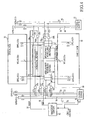
- A typical processor based system which includes a memory device according to the present invention is illustrated generally at 200 in
FIG. 7 . A computer system is exemplary of a system having digital circuits which include memory devices. Most conventional computers include memory devices permitting storage of significant amounts of data. The data is accessed during operation of the computers. Other types of dedicated processing systems, e. g., radio systems, television systems, GPS receiver systems, telephones and telephone systems also contain memory devices which can utilize the present invention. - A processor based system, such as a computer system, for example, generally comprises a central processing unit (CPU) 210, for example, a microprocessor, that communicates with one or more input/output (I/O)
devices 240 over abus 270. Thecomputer system 200 also includes random access memory (RAM) such asDRAM 260, and, in the case of a computer system may include peripheral devices such as afloppy disk drive 220 and a compact disk (CD)ROM drive 230 which also communicate withCPU 210 over thebus 270.RAM 260 is preferably constructed as an integrated circuit which includes circuitry to allow for segmented row repair as previously described with respect toFigs. 4-6 . It may also be desirable to integrate theprocessor 210 andmemory 260 on a single IC chip. - It should be noted that while the preferred embodiment of the invention is described as applied to a 256 Mbit memory DRAM device having typical row addressable architecture, the invention is not so limited and may be applied to memory devices having other architectures or sizes as well. Additionally, while the invention has been described with reference to segmenting the rows into four segments, the invention is not so limited and any number of segments can be used.
- While preferred embodiments of the invention have been described and illustrated above, it should be understood that these are exemplary of the invention and are not to be considered as limiting. Additions, deletions, substitutions, and other modifications can be made without departing from the spirit or scope of the present invention. Accordingly, the invention is not to be considered as limited by the foregoing description but is only limited by the scope of the appended claims.
Claims (9)
- A memory device comprising:a memory array comprising primary memory cells;at least one primary row wordline for accessing a row of said primary memory cells, said at least one primary row wordline being divided into a plurality of segments, each of which accesses a respective portion of said row of said primary memory cells;at least one row of redundant memory cells;at least one redundant row wordline for accessing said redundant memory cells, said at least one redundant row wordline being divided into a plurality of segments, each of which accesses a portion of said redundant memory cells; anda programmable logic circuit which can be selectively programmed to replace at least one of said primary row wordline segments associated with a defective memory cell with a redundant row wordline segment during memory access operation.
- The memory device according to Claim 1, wherein said programmable logic circuit further comprises:a plurality of AND gates, each of said plurality of AND gates having a first input coupled to receive one of a plurality of first control signals, a second input coupled to receive on of a plurality of second control signals, and an output coupled to a driver associated with a respective one of said at least one primary row wordline and said at least one redundant row wordline.
- The memory device according to Claim 2, wherein said plurality of first control signals are respective phase signals.
- The memory device according to Claim 2, further comprising:a matching circuit to compare an input memory cell address to an address of said defective memory cell and output said plurality of second control signals based on said comparison.
- A processor system comprising:a central processing unit; anda memory device connected to said central processing unit to receive data from and supply data to said central processing unit, said memory device comprising:a memory array comprising primary memory cells;at least one primary row wordline for accessing a row of said primary memory cells, said at least one primary row wordline being divided into a plurality of segments, each of which accesses a respective portion of said row of said primary memory cells;at least one row of redundant memory cells;at least one redundant row wordline for accessing said redundant memory cells, said at least one redundant row wordline being divided into a plurality of segments, each of which accesses a portion of said redundant memory cells; anda programmable logic circuit which can be selectively programmed to replace at least one of said primary row wordline segments associated with a defective memory cell with a redundant row wordline segment during memory access operation.
- The processor system according to Claim 5, wherein said programmable logic circuit further comprises:a plurality of AND gates, each of said plurality of AND gates having a first input coupled to receive one of a plurality of first control signals, a second input coupled to receive on of a plurality of second control signals, and an output coupled to a driver associated with a respective one of said at least one primary row wordline and said at least one redundant row wordline.
- The processor system according to Claim 6, wherein said plurality of first control signals are respective phase signals.
- The processor system according to Claim 6, further comprising:a matching circuit to compare an input memory cell address to an address of said defective memory cell and output said plurality of second control signals based on said comparison.
- A method for repairing out a defective memory cell in a memory device, said method comprising:locating said defective memory cell in said memory device;identifying a segment of a row of memory blocks in which said defective memory cell is located;disabling a driver associated with a portion of a primary memory cell row in which said defective memory cell is located in only said identified segment;enabling a driver associated with a redundant memory cell row in only said identified segment; andrepairing out said defective memory cell with said redundant memory cell row in only said portion of the primary memory cell row located in said identified segment.
Applications Claiming Priority (2)
| Application Number | Priority Date | Filing Date | Title |
|---|---|---|---|
| US09/594,442 US6314030B1 (en) | 2000-06-14 | 2000-06-14 | Semiconductor memory having segmented row repair |
| EP01942036A EP1292952B8 (en) | 2000-06-14 | 2001-06-07 | Semiconductor memory having segmented row repair |
Related Parent Applications (1)
| Application Number | Title | Priority Date | Filing Date |
|---|---|---|---|
| EP01942036A Division EP1292952B8 (en) | 2000-06-14 | 2001-06-07 | Semiconductor memory having segmented row repair |
Publications (1)
| Publication Number | Publication Date |
|---|---|
| EP2058820A1 true EP2058820A1 (en) | 2009-05-13 |
Family
ID=24378869
Family Applications (2)
| Application Number | Title | Priority Date | Filing Date |
|---|---|---|---|
| EP09001943A Withdrawn EP2058820A1 (en) | 2000-06-14 | 2001-06-07 | Semiconductor memory having segmented row repair |
| EP01942036A Expired - Lifetime EP1292952B8 (en) | 2000-06-14 | 2001-06-07 | Semiconductor memory having segmented row repair |
Family Applications After (1)
| Application Number | Title | Priority Date | Filing Date |
|---|---|---|---|
| EP01942036A Expired - Lifetime EP1292952B8 (en) | 2000-06-14 | 2001-06-07 | Semiconductor memory having segmented row repair |
Country Status (10)
| Country | Link |
|---|---|
| US (2) | US6314030B1 (en) |
| EP (2) | EP2058820A1 (en) |
| JP (1) | JP2004503897A (en) |
| KR (1) | KR100595813B1 (en) |
| CN (2) | CN101471140A (en) |
| AT (1) | ATE428175T1 (en) |
| AU (1) | AU2001275334A1 (en) |
| DE (1) | DE60138283D1 (en) |
| ES (1) | ES2325056T3 (en) |
| WO (1) | WO2001097226A2 (en) |
Cited By (1)
| Publication number | Priority date | Publication date | Assignee | Title |
|---|---|---|---|---|
| KR20210006616A (en) * | 2019-07-09 | 2021-01-19 | 삼성전자주식회사 | Semiconductor memory devices and methods of operating semiconductor memory devices |
Families Citing this family (26)
| Publication number | Priority date | Publication date | Assignee | Title |
|---|---|---|---|---|
| US6163489A (en) | 1999-07-16 | 2000-12-19 | Micron Technology Inc. | Semiconductor memory having multiple redundant columns with offset segmentation boundaries |
| KR20020002133A (en) * | 2000-06-29 | 2002-01-09 | 박종섭 | Column redundancy circuit |
| US6625081B2 (en) | 2001-08-13 | 2003-09-23 | Micron Technology, Inc. | Synchronous flash memory with virtual segment architecture |
| US6687171B2 (en) * | 2002-04-26 | 2004-02-03 | Infineon Technologies Aktiengesellschaft | Flexible redundancy for memories |
| US6621751B1 (en) | 2002-06-04 | 2003-09-16 | Micron Technology, Inc. | Method and apparatus for programming row redundancy fuses so decoding matches internal pattern of a memory array |
| KR100468315B1 (en) * | 2002-07-15 | 2005-01-27 | 주식회사 하이닉스반도체 | Repair circuit |
| US6807114B2 (en) * | 2003-01-17 | 2004-10-19 | Micron Technology, Inc. | Method and system for selecting redundant rows and columns of memory cells |
| US7509543B2 (en) * | 2003-06-17 | 2009-03-24 | Micron Technology, Inc. | Circuit and method for error test, recordation, and repair |
| US6868019B2 (en) * | 2003-07-02 | 2005-03-15 | Micron Technology, Inc. | Reduced power redundancy address decoder and comparison circuit |
| US6992937B2 (en) * | 2003-07-28 | 2006-01-31 | Silicon Storage Technology, Inc. | Column redundancy for digital multilevel nonvolatile memory |
| US7061815B2 (en) * | 2003-08-05 | 2006-06-13 | Stmicroelectronics Pvt. Ltd. | Semiconductor memory device providing redundancy |
| DE102004036545B3 (en) * | 2004-07-28 | 2006-03-16 | Infineon Technologies Ag | Integrated semiconductor memory with redundant memory cells |
| US20080291760A1 (en) * | 2007-05-23 | 2008-11-27 | Micron Technology, Inc. | Sub-array architecture memory devices and related systems and methods |
| US7885128B2 (en) | 2008-10-21 | 2011-02-08 | Micron Technology, Inc. | Redundant memory array for replacing memory sections of main memory |
| US8331126B2 (en) | 2010-06-28 | 2012-12-11 | Qualcomm Incorporated | Non-volatile memory with split write and read bitlines |
| CN102456414B (en) * | 2010-10-20 | 2014-11-26 | 旺宏电子股份有限公司 | Memory device with backup line and repair method thereof |
| DE112011106030B4 (en) | 2011-12-23 | 2019-10-02 | Intel Corporation | Auto repair logic for a stack architecture |
| CN105513647A (en) * | 2011-12-23 | 2016-04-20 | 英特尔公司 | Self-repair logic for stacked storage device structure |
| TWI497517B (en) * | 2012-11-02 | 2015-08-21 | Elite Semiconductor Esmt | Repairing circuit for memory circuit and method thereof and memory circuit using the same |
| KR20160002820A (en) * | 2013-04-24 | 2016-01-08 | 휴렛-팩커드 디벨롭먼트 컴퍼니, 엘.피. | Representing data using a group of multilevel memory cells |
| KR102204390B1 (en) | 2014-09-12 | 2021-01-18 | 삼성전자주식회사 | Memory device with fast fail cell repair |
| KR20160120006A (en) * | 2015-04-07 | 2016-10-17 | 에스케이하이닉스 주식회사 | Semiconductor memory device |
| CN113299336B (en) * | 2020-02-24 | 2024-06-28 | 长鑫存储技术(上海)有限公司 | Repair circuit, memory and repair method |
| US11164610B1 (en) | 2020-06-05 | 2021-11-02 | Qualcomm Incorporated | Memory device with built-in flexible double redundancy |
| US11177010B1 (en) | 2020-07-13 | 2021-11-16 | Qualcomm Incorporated | Bitcell for data redundancy |
| US11114181B1 (en) * | 2020-08-03 | 2021-09-07 | Micron Technology, Inc. | Memory devices with redundant memory cells for replacing defective memory cells, and related systems and methods |
Citations (4)
| Publication number | Priority date | Publication date | Assignee | Title |
|---|---|---|---|---|
| US5446698A (en) * | 1994-06-30 | 1995-08-29 | Sgs-Thomson Microelectronics, Inc. | Block decoded redundant master wordline |
| US5774471A (en) * | 1996-12-17 | 1998-06-30 | Integrated Silicon Solution Inc. | Multiple location repair word line redundancy circuit |
| US5808945A (en) * | 1996-02-21 | 1998-09-15 | Sony Corporation | Semiconductor memory having redundant memory array |
| US6005813A (en) * | 1997-11-12 | 1999-12-21 | Micron Technology, Inc. | Device and method for repairing a semiconductor memory |
Family Cites Families (23)
| Publication number | Priority date | Publication date | Assignee | Title |
|---|---|---|---|---|
| US4918622A (en) | 1988-11-16 | 1990-04-17 | Eastman Kodak Company | Electronic graphic arts screener |
| US5126973A (en) * | 1990-02-14 | 1992-06-30 | Texas Instruments Incorporated | Redundancy scheme for eliminating defects in a memory device |
| KR960002777B1 (en) | 1992-07-13 | 1996-02-26 | 삼성전자주식회사 | Low Redundancy Devices in Semiconductor Memory Devices |
| DE59310168D1 (en) * | 1993-02-19 | 2001-06-07 | Infineon Technologies Ag | Column redundancy circuitry for a memory |
| JP3077868B2 (en) * | 1993-12-27 | 2000-08-21 | 日本電気株式会社 | Semiconductor storage circuit device |
| US5625725A (en) | 1993-12-28 | 1997-04-29 | Sony Corporation | Magneto-optical pickup device having phase compensating circuitry |
| JP3386547B2 (en) * | 1994-01-26 | 2003-03-17 | 株式会社東芝 | Redundancy circuit device |
| US5528539A (en) | 1994-09-29 | 1996-06-18 | Micron Semiconductor, Inc. | High speed global row redundancy system |
| JPH08227597A (en) * | 1995-02-21 | 1996-09-03 | Mitsubishi Electric Corp | Semiconductor memory device |
| JP3774500B2 (en) | 1995-05-12 | 2006-05-17 | 株式会社ルネサステクノロジ | Semiconductor memory device |
| US5532966A (en) * | 1995-06-13 | 1996-07-02 | Alliance Semiconductor Corporation | Random access memory redundancy circuit employing fusible links |
| JP3710002B2 (en) * | 1995-08-23 | 2005-10-26 | 株式会社日立製作所 | Semiconductor memory device |
| JPH09231789A (en) * | 1996-02-21 | 1997-09-05 | Sony Corp | Semiconductor memory device |
| DE69618928D1 (en) | 1996-04-18 | 2002-03-14 | St Microelectronics Srl | Semiconductor memory device with line redundancy |
| US5706292A (en) | 1996-04-25 | 1998-01-06 | Micron Technology, Inc. | Layout for a semiconductor memory device having redundant elements |
| US5732030A (en) * | 1996-06-25 | 1998-03-24 | Texas Instruments Incorporated | Method and system for reduced column redundancy using a dual column select |
| US5815447A (en) | 1996-08-08 | 1998-09-29 | Micron Technology, Inc. | Memory device having complete row redundancy |
| DE19729579C2 (en) * | 1997-07-10 | 2000-12-07 | Siemens Ag | Method for activating a redundant word line with inter-segment redundancy in a semiconductor memory with word lines organized in segments |
| JP3204190B2 (en) * | 1997-12-26 | 2001-09-04 | 日本電気株式会社 | Semiconductor storage device |
| JPH11339493A (en) | 1998-05-27 | 1999-12-10 | Mitsubishi Electric Corp | Synchronous semiconductor memory device |
| JP3908392B2 (en) * | 1998-07-31 | 2007-04-25 | エルピーダメモリ株式会社 | Semiconductor integrated circuit device |
| US6157584A (en) * | 1999-05-20 | 2000-12-05 | Advanced Micro Devices, Inc. | Redundancy circuit and method for semiconductor memory |
| US6163489A (en) * | 1999-07-16 | 2000-12-19 | Micron Technology Inc. | Semiconductor memory having multiple redundant columns with offset segmentation boundaries |
-
2000
- 2000-06-14 US US09/594,442 patent/US6314030B1/en not_active Expired - Lifetime
-
2001
- 2001-06-07 ES ES01942036T patent/ES2325056T3/en not_active Expired - Lifetime
- 2001-06-07 CN CNA2008101766900A patent/CN101471140A/en active Pending
- 2001-06-07 EP EP09001943A patent/EP2058820A1/en not_active Withdrawn
- 2001-06-07 KR KR1020027017053A patent/KR100595813B1/en not_active Expired - Lifetime
- 2001-06-07 AU AU2001275334A patent/AU2001275334A1/en not_active Abandoned
- 2001-06-07 AT AT01942036T patent/ATE428175T1/en not_active IP Right Cessation
- 2001-06-07 JP JP2002511339A patent/JP2004503897A/en active Pending
- 2001-06-07 WO PCT/US2001/018388 patent/WO2001097226A2/en not_active Ceased
- 2001-06-07 EP EP01942036A patent/EP1292952B8/en not_active Expired - Lifetime
- 2001-06-07 DE DE60138283T patent/DE60138283D1/en not_active Expired - Lifetime
- 2001-06-07 CN CNB018131034A patent/CN100442434C/en not_active Expired - Lifetime
- 2001-08-14 US US09/928,404 patent/US6442084B2/en not_active Expired - Lifetime
Patent Citations (4)
| Publication number | Priority date | Publication date | Assignee | Title |
|---|---|---|---|---|
| US5446698A (en) * | 1994-06-30 | 1995-08-29 | Sgs-Thomson Microelectronics, Inc. | Block decoded redundant master wordline |
| US5808945A (en) * | 1996-02-21 | 1998-09-15 | Sony Corporation | Semiconductor memory having redundant memory array |
| US5774471A (en) * | 1996-12-17 | 1998-06-30 | Integrated Silicon Solution Inc. | Multiple location repair word line redundancy circuit |
| US6005813A (en) * | 1997-11-12 | 1999-12-21 | Micron Technology, Inc. | Device and method for repairing a semiconductor memory |
Cited By (1)
| Publication number | Priority date | Publication date | Assignee | Title |
|---|---|---|---|---|
| KR20210006616A (en) * | 2019-07-09 | 2021-01-19 | 삼성전자주식회사 | Semiconductor memory devices and methods of operating semiconductor memory devices |
Also Published As
| Publication number | Publication date |
|---|---|
| US6442084B2 (en) | 2002-08-27 |
| CN100442434C (en) | 2008-12-10 |
| EP1292952B8 (en) | 2009-08-05 |
| WO2001097226A3 (en) | 2002-05-10 |
| EP1292952B1 (en) | 2009-04-08 |
| US20010053101A1 (en) | 2001-12-20 |
| AU2001275334A1 (en) | 2001-12-24 |
| DE60138283D1 (en) | 2009-05-20 |
| ES2325056T3 (en) | 2009-08-25 |
| CN101471140A (en) | 2009-07-01 |
| KR100595813B1 (en) | 2006-07-03 |
| ATE428175T1 (en) | 2009-04-15 |
| WO2001097226A2 (en) | 2001-12-20 |
| US6314030B1 (en) | 2001-11-06 |
| JP2004503897A (en) | 2004-02-05 |
| CN1636260A (en) | 2005-07-06 |
| EP1292952A2 (en) | 2003-03-19 |
| KR20030009526A (en) | 2003-01-29 |
Similar Documents
| Publication | Publication Date | Title |
|---|---|---|
| EP1292952B1 (en) | Semiconductor memory having segmented row repair | |
| US6163489A (en) | Semiconductor memory having multiple redundant columns with offset segmentation boundaries | |
| US11651831B2 (en) | Redundancy analysis circuit and memory system including the same | |
| US6145092A (en) | Apparatus and method implementing repairs on a memory device | |
| US7120068B2 (en) | Column/row redundancy architecture using latches programmed from a look up table | |
| KR0158510B1 (en) | Semiconductor memory device with redundant decoder available for test sequence on redundant memory cells | |
| US4355376A (en) | Apparatus and method for utilizing partially defective memory devices | |
| US6693833B2 (en) | Device and method for repairing a semiconductor memory | |
| EP1221165B1 (en) | Circuit and method for a multiplexed redundancy scheme in a memory device | |
| US6097644A (en) | Redundant row topology circuit, and memory device and test system using same | |
| US5278793A (en) | Memory defect masking device | |
| KR100395031B1 (en) | Integrated semiconductor memory with redundant unit of memory cells | |
| US5544113A (en) | Random access memory having a flexible array redundancy scheme | |
| US5793683A (en) | Wordline and bitline redundancy with no performance penalty | |
| KR100963552B1 (en) | Semiconductor memory | |
| EP1408512B1 (en) | Method for storing errors of a memory device in a diagnose array having a minimum storing size | |
| US6567324B2 (en) | Semiconductor memory device with reduced number of redundant program sets | |
| US6754113B2 (en) | Topography correction for testing of redundant array elements | |
| JP2007048458A (en) | Semiconductor memory device |
Legal Events
| Date | Code | Title | Description |
|---|---|---|---|
| PUAI | Public reference made under article 153(3) epc to a published international application that has entered the european phase |
Free format text: ORIGINAL CODE: 0009012 |
|
| 17P | Request for examination filed |
Effective date: 20090216 |
|
| AC | Divisional application: reference to earlier application |
Ref document number: 1292952 Country of ref document: EP Kind code of ref document: P |
|
| AK | Designated contracting states |
Kind code of ref document: A1 Designated state(s): AT BE CH CY DE DK ES FI FR GB GR IE IT LI LU MC NL PT SE TR |
|
| RAP1 | Party data changed (applicant data changed or rights of an application transferred) |
Owner name: MOSAID TECHNOLOGIES INCORPORATED |
|
| AKX | Designation fees paid |
Designated state(s): AT BE CH CY DE DK ES FI FR GB GR IE IT LI LU MC NL PT SE TR |
|
| GRAP | Despatch of communication of intention to grant a patent |
Free format text: ORIGINAL CODE: EPIDOSNIGR1 |
|
| STAA | Information on the status of an ep patent application or granted ep patent |
Free format text: STATUS: THE APPLICATION IS DEEMED TO BE WITHDRAWN |
|
| 18D | Application deemed to be withdrawn |
Effective date: 20111216 |