EP2058134A1 - Thermal print head and method for manufacturing the same - Google Patents
Thermal print head and method for manufacturing the same Download PDFInfo
- Publication number
- EP2058134A1 EP2058134A1 EP07793006A EP07793006A EP2058134A1 EP 2058134 A1 EP2058134 A1 EP 2058134A1 EP 07793006 A EP07793006 A EP 07793006A EP 07793006 A EP07793006 A EP 07793006A EP 2058134 A1 EP2058134 A1 EP 2058134A1
- Authority
- EP
- European Patent Office
- Prior art keywords
- glaze
- electrodes
- heating
- insulating film
- heating resistor
- Prior art date
- Legal status (The legal status is an assumption and is not a legal conclusion. Google has not performed a legal analysis and makes no representation as to the accuracy of the status listed.)
- Withdrawn
Links
Images



Classifications
-
- B—PERFORMING OPERATIONS; TRANSPORTING
- B41—PRINTING; LINING MACHINES; TYPEWRITERS; STAMPS
- B41J—TYPEWRITERS; SELECTIVE PRINTING MECHANISMS, i.e. MECHANISMS PRINTING OTHERWISE THAN FROM A FORME; CORRECTION OF TYPOGRAPHICAL ERRORS
- B41J2/00—Typewriters or selective printing mechanisms characterised by the printing or marking process for which they are designed
- B41J2/315—Typewriters or selective printing mechanisms characterised by the printing or marking process for which they are designed characterised by selective application of heat to a heat sensitive printing or impression-transfer material
- B41J2/32—Typewriters or selective printing mechanisms characterised by the printing or marking process for which they are designed characterised by selective application of heat to a heat sensitive printing or impression-transfer material using thermal heads
- B41J2/335—Structure of thermal heads
- B41J2/33505—Constructional details
- B41J2/3353—Protective layers
-
- B—PERFORMING OPERATIONS; TRANSPORTING
- B41—PRINTING; LINING MACHINES; TYPEWRITERS; STAMPS
- B41J—TYPEWRITERS; SELECTIVE PRINTING MECHANISMS, i.e. MECHANISMS PRINTING OTHERWISE THAN FROM A FORME; CORRECTION OF TYPOGRAPHICAL ERRORS
- B41J2/00—Typewriters or selective printing mechanisms characterised by the printing or marking process for which they are designed
- B41J2/315—Typewriters or selective printing mechanisms characterised by the printing or marking process for which they are designed characterised by selective application of heat to a heat sensitive printing or impression-transfer material
- B41J2/32—Typewriters or selective printing mechanisms characterised by the printing or marking process for which they are designed characterised by selective application of heat to a heat sensitive printing or impression-transfer material using thermal heads
- B41J2/335—Structure of thermal heads
- B41J2/3355—Structure of thermal heads characterised by materials
-
- Y—GENERAL TAGGING OF NEW TECHNOLOGICAL DEVELOPMENTS; GENERAL TAGGING OF CROSS-SECTIONAL TECHNOLOGIES SPANNING OVER SEVERAL SECTIONS OF THE IPC; TECHNICAL SUBJECTS COVERED BY FORMER USPC CROSS-REFERENCE ART COLLECTIONS [XRACs] AND DIGESTS
- Y10—TECHNICAL SUBJECTS COVERED BY FORMER USPC
- Y10T—TECHNICAL SUBJECTS COVERED BY FORMER US CLASSIFICATION
- Y10T29/00—Metal working
- Y10T29/49—Method of mechanical manufacture
- Y10T29/49401—Fluid pattern dispersing device making, e.g., ink jet
Definitions
- the present invention relates to a thermal printhead for performing printing on a recording medium such as a thermal paper.
- the present invention also relates to a method for manufacturing a thermal printhead.
- Fig. 9 shows an example of conventional thermal printhead.
- a heating resistor 93, electrodes 94A, 94B and a protective film 95 are laminated on a substrate 91 formed with a glaze 92.
- the portion of the heating resistor 93 which is sandwiched between the electrodes 94A and 94B serves as a heating portion 93a.
- the glaze 92 is made of e.g. glass and bulges in the thickness direction of the substrate 91 in cross section.
- the glaze 92 has a relatively low thermal conductivity and prevents the heat from the heating portion 93a from unduly escaping to the substrate 91.
- the heating portion 93a is located at a position retreated from a recording medium relative to the electrodes 94A and 94B.
- a structure like this is also disclosed in Fig. 1 of Patent Document 1 identified below. With this structure, however, of the protective film 95, the portion covering the heating portion 93a is pressed against a recording medium with a relatively small pressure, which hinders an increase in the printing speed.
- Patent Document 1 JP-A-2001-246770
- the present invention has been proposed under the circumstances described above. It is, therefore, an object of the present invention to provide a thermal printhead which is capable of increasing the printing speed.
- a thermal printhead comprising a substrate, a glaze formed on the substrate and extending in the primary scanning direction, a first and a second electrodes overlapping the glaze and spaced from each other in the secondary scanning direction, a heating resistor overlapping the first and the second electrodes and including a heat generating portion spaced apart from the electrodes, and an insulating film intervening between at least part of the heating portion of the heating resistor and the glaze. At least an end of each of the electrodes is embedded in the glaze.
- the insulating film has a hardness which is higher than the hardness of the glaze and lower than the hardness of the heating resistor and a thermal conductivity which is higher than the thermal conductivity of the glaze and lower than the thermal conductivity of the heating resistor.
- the level difference between each of the electrodes and the glaze is reduced. Further, owing to the existence of the insulating film, the heating portion is positioned close to a recording medium. As a result, the portion of the protective film which covers the heating portion is pressed against a recording medium with a high pressure. Thus, the printing speed can be increased. Moreover, the heat from the heating portion is transferred to the glaze via the insulating film. Thus, the amount of heat which the glaze receives is prevented from suddenly increasing or decreasing. As a result, the thermal stress generated in the glaze reduces, whereby the glaze is prevented from cracking. Further, the insulating film functions as a buffer between the glaze and the heating resistor. Thus, the thermal expansion or contraction of the glaze is prevented from being suppressed or promoted by the heating resistor. This is suitable for preventing the glaze from cracking.
- the insulating film is formed to bridge the first and the second electrodes.
- the region of the glaze which is positioned between the first and the second electrodes is completely covered.
- the heating resistor and the glaze do not come into contact with each other at all, which is preferable for preventing the glaze from cracking.
- the insulating film is made of either one of Ta 2 O 5 and SiO 2 . This arrangement is suitable for achieving the above-described hardness and thermal conductivity of the insulating film.
- a method for manufacturing a thermal printhead comprises the steps of forming a glaze extending in the primary scanning direction on a substrate and forming a first and a second electrodes spaced from each other in the secondary scanning direction on the glaze, sinking at least an end of each of the electrodes into the glaze by softening at least part of the glaze by heating, forming an insulating film to cover at least part of a region of the glaze which is sandwiched between the first and the second electrodes, and forming a heating resistor to overlap the glaze and the first and the second electrodes in such a manner as to bridge the first and the second electrodes.
- the insulating film is formed to have a hardness which is higher than the hardness of the glaze and lower than the hardness of the heating resistor and a thermal conductivity which is higher than the thermal conductivity of the glaze and lower than the thermal conductivity of the heating resistor.
- Figs. 1 and 2 show a thermal printhead according to a first embodiment of the present invention.
- the illustrated thermal printhead A1 includes a substrate 1, a glaze 2, a plurality of first electrodes 3A, a plurality of second electrodes 3B, insulating films 4, heating resistors 5 and a protective film 6.
- a protective film 6 For easier understanding, only the electrodes 3A, 3B, the insulating films 4 and the heating resistors 5 are shown in Fig. 2 .
- the substrate 1 is a flat insulating plate which is in the form of an elongated rectangle extending in the primary scanning direction as viewed in plan and made of e.g. alumina ceramic material.
- the glaze 2 is formed on the substrate 1 by printing and baking amorphous glass paste, for example.
- the glaze 2 serves to retain heat and provide a smooth surface on which the electrodes 3A and 3B are to be formed.
- the glaze 2 is elongated in the primary scanning direction and bulges in the thickness direction of the substrate 1 in cross section. Due to this shape, the glaze 2 enhances the contact pressure between a recording medium such as thermal paper and the portion of the protective film 6 which covers the heating portion 5a, which will be described later.
- the maximum thickness of the glaze 2 is about 50 ⁇ m.
- the first and the second electrodes 3A and 3B are formed in pairs on the substrate 1 and the glaze 2 by e.g. printing and baking gold resinate paste. As shown in Fig. 2 , the first electrode 3A and the second electrode 3B of each pair are spaced from each other in the secondary scanning direction, with respective ends 31A and 31B facing each other. As shown in Fig. 1 , the ends 31A and 31B are embedded in the glaze 2, and the upper surfaces of the ends 31A, 31B and the upper surface of the glaze 2 (the surface which is not covered with the ends 31A, 31B) forms a smooth curved surface free from a stepped portion.
- the electrodes 3A and 3B have a thickness of about 0.6 ⁇ m.
- the insulating films 4 are made of e.g. Ta 2 O 5 and formed by baking Ta films formed by sputtering, for example.
- the insulating films 4 cover the regions of the glaze 2 which are sandwiched between the paired electrodes 3A and 3B.
- each of the insulating films 4 partially overlaps the ends 31A and 31B of the paired electrodes. That is, each insulating film 4 extends in such a manner as to bridge the paired electrodes 3A and 3B.
- the insulating film 4 has a thickness of about 0.1 to 0.2 ⁇ m.
- the hardness of the insulating film 4 is higher than that of the glaze 2 and lower than that of the heating resistors 5.
- the thermal conductivity of the insulating film 4 is higher than that of the glaze 2 and lower than that of the heating resistors 5.
- the insulating film 4 may be made of SiO 2 instead of Ta 2 O 5 .
- the heating resistors 5 are formed on the insulating films 4 in such a manner as to bridge the electrodes 3A and 3B.
- the heating resistors 5 are made of e.g. TaSiO 2 .
- the portion which is not in direct contact with the electrodes 3A and 3B provides a heating portion 5a (see the diagonally shaded portion in Fig. 2 ).
- the heating portion 5a generates heat.
- the thermal printhead A1 performs printing on a recording medium such as thermal paper.
- the width of the heating resistor 5 is smaller than that of the insulating film 4.
- the heating resistor 5 has a thickness of 0.05 ⁇ m.
- the protective film 6 covers the glaze 2, the electrodes 3A, 3B, the insulating films 4 and the heating resistors 5.
- the protective film 6 is formed by e.g. sputtering using SiC or SiAlON.
- the protective film 6 prevents the electrodes 3A, 3B and the heating resistors 5 from coming into direct contact with a recording medium or being affected chemically or electrically.
- the protective film 6 also serves to provide a smooth surface.
- the thickness of the protective film 6 is about 4.0 ⁇ m.
- thermal printhead A1 A method for manufacturing the thermal printhead A1 will be described below with reference to Figs. 3-6 .
- a glaze 2 is formed on a substrate 1. This is performed by printing and baking amorphous glass paste. Specifically, on the substrate 1, glass paste is first printed in the form of a strip extending in the primary scanning direction. Then, the glass paste is baked. As a result, a glaze 2 is obtained which has a maximum thickness of about 50 ⁇ m and bulges in the thickness direction of the substrate 1 in cross section.
- electrodes 3A and 3B are formed on the upper surfaces of the substrate 1 and glaze 2. Specifically, first, gold resinate paste is printed in the form of a film on the upper surfaces of the substrate 1 and glaze 2, and then, the film is baked. Then, the baked paste film is subjected to patterning, whereby electrodes 3A and 3B are obtained. The amount of gold resinate paste to be applied and so on is so set in advance that the electrodes 3A and 3B have a thickness of about 0.6 ⁇ m.
- the ends 31A and 31B of the electrodes 3A and 3B are sunk into the glaze 2.
- This process can be achieved by softening the glaze 2 by heating. Specifically, the glaze 2 is heated at a temperature in the range from the glass softening point to the glass transition point of the glass component contained in the glaze 2.
- the ends 31A and 31B are sunk into the glaze 2 by their own weight.
- the amount of sinking can be adjusted by controlling the temperature or time of the heating.
- insulating films 4 are formed.
- a film of Ta is formed by sputtering to bridge the ends 31A and 31B of each electrode pair 3A and 3B.
- the Ta film is baked for oxidation.
- an insulating film 4 made of Ta 2 O 5 is obtained.
- the thickness of the insulating film 4 is set to about 0.1 to 0.2 ⁇ m.
- the insulating film 4 may be made of SiO 2 instead of Ta 2 O 5 .
- heating resistors 5 covering the insulating films 4 and bridging the electrodes 3A and 3B are made by forming e.g. a TaSiO 2 film having a thickness of about 0.05 ⁇ m and then subjecting the film to dry etching. Thereafter, by sputtering using e.g. SiC or SiAlON, a protective film 6 is formed to cover the electrodes 3A, 3B and the heating resistors 5.
- the thermal printhead A1 as shown in Figs. 1 and 2 is obtained.
- thermal printhead A1 The advantages of the thermal printhead A1 will be described below.
- a stepped portion is not provided between each of the electrodes 3A, 3B and the glaze 2. Further, owing to the existence of the insulating films 4, the heating portions 5a are positioned close to a recording medium. As a result, the portions of the protective film 6 which cover the heating portions 5a are pressed against a recording medium with a high pressure. Thus, the printing speed of the thermal printhead A1 can be increased.
- the heat from the heating portions 5a is transferred to the glaze 2 via the insulating films 4.
- the degree of increase or decrease of the heat the glaze 2 receives can be smaller.
- the thermal stress generated in the glaze 2 reduces, whereby the glaze 2 is prevented from cracking.
- the insulating films 4 function as a mechanical buffer between the glaze 2 and the heating resistors 5.
- the thermal expansion or contraction of the glaze 2 (which has a relatively low hardness) is prevented from being suppressed or promoted by the heating resistors 5 (which have a relatively high hardness). This is suitable for preventing the glaze 2 from cracking.
- the insulating films 4 have a hardness of a level between the hardness of the glaze 2 and that of the heating resistors 5 and a thermal conductivity of a level between the thermal conductivity of the glaze 2 and that of the heating resistors 5, it is preferable to form the insulating films 4 using Ta 2 O 5 .
- the region of the glaze 2 which is located between the electrodes 3A and 3B is entirely covered with the insulating film 4. With this structure, the heating resistor 5 and the glaze 2 do not come into contact with each other, which is advantageous for preventing the glaze 2 from cracking.
- Figs. 7 and 8 show other embodiments of the present invention.
- the elements which are identical or similar to those of the first embodiment are designated by the same reference signs as those used for the first embodiment.
- Fig. 7 shows a thermal printhead according to a second embodiment of the present invention.
- the illustrated thermal printhead A2 includes a dummy pattern 3C.
- the dummy pattern 3C is made of e.g. Au and has a relatively high thermal conductivity.
- the dummy pattern 3C comprises a plurality of elements spaced from each other in the secondary scanning direction.
- the dummy pattern 3C is formed along with the electrodes 3A and 3B by thick-film printing and baking. Similarly to the electrodes 3A and 3B, the dummy pattern 3C is embedded in the glaze 2 and flush with the glaze 2.
- Fig. 8 shows a thermal printhead according to a third embodiment of the present invention.
- the illustrated thermal printhead A3 differs from the foregoing two embodiments in positional relationship among the glaze 2, the electrodes 3A, 3B and the insulating films 4.
- the ends 31A and 31B of the electrodes 3A and 3B are sunk in the glaze 2, the amount of sinking is smaller than the thickness of the ends 31A and 31B.
- the level difference is substantially equal to the thickness of the insulating film 4.
- the insulating film 4 is located only between the electrodes 3A and 3B, and does not extend onto the electrodes 3A and 3B.
- the heating resistor 5 is formed on a relatively smooth surface.
- the heating resistor 5 is prevented from having a non-uniform thickness and breaking due to e.g. the pressure applied in the printing process.
Landscapes
- Electronic Switches (AREA)
Abstract
Description
- The present invention relates to a thermal printhead for performing printing on a recording medium such as a thermal paper. The present invention also relates to a method for manufacturing a thermal printhead.
-
Fig. 9 shows an example of conventional thermal printhead. In the thermal printhead X shown in the figure, a heating resistor 93,electrodes protective film 95 are laminated on asubstrate 91 formed with aglaze 92. The portion of the heating resistor 93 which is sandwiched between theelectrodes heating portion 93a. Theglaze 92 is made of e.g. glass and bulges in the thickness direction of thesubstrate 91 in cross section. Theglaze 92 has a relatively low thermal conductivity and prevents the heat from theheating portion 93a from unduly escaping to thesubstrate 91. - In the thermal printhead X, the
heating portion 93a is located at a position retreated from a recording medium relative to theelectrodes Fig. 1 ofPatent Document 1 identified below. With this structure, however, of theprotective film 95, the portion covering theheating portion 93a is pressed against a recording medium with a relatively small pressure, which hinders an increase in the printing speed. - Moreover, as the printing speed increases, the heating cycle of the
heating portion 93a shortens. Since theheating portion 93a is directly formed on theglaze 92, the cycle in which theglaze 92 receives heat also shortens. Thus, during the printing operation by the thermal printhead X, theglaze 92 is kept at a relatively high temperature while repeating temperature rise and temperature drop. As a result, excessive thermal stress is applied on theglaze 92, which may cause cracking of theglaze 92.
Patent Document 1:JP-A-2001-246770 - The present invention has been proposed under the circumstances described above. It is, therefore, an object of the present invention to provide a thermal printhead which is capable of increasing the printing speed.
- According to a first aspect of the present invention, there is provided a thermal printhead comprising a substrate, a glaze formed on the substrate and extending in the primary scanning direction, a first and a second electrodes overlapping the glaze and spaced from each other in the secondary scanning direction, a heating resistor overlapping the first and the second electrodes and including a heat generating portion spaced apart from the electrodes, and an insulating film intervening between at least part of the heating portion of the heating resistor and the glaze. At least an end of each of the electrodes is embedded in the glaze. The insulating film has a hardness which is higher than the hardness of the glaze and lower than the hardness of the heating resistor and a thermal conductivity which is higher than the thermal conductivity of the glaze and lower than the thermal conductivity of the heating resistor.
- With this structure, the level difference between each of the electrodes and the glaze is reduced. Further, owing to the existence of the insulating film, the heating portion is positioned close to a recording medium. As a result, the portion of the protective film which covers the heating portion is pressed against a recording medium with a high pressure. Thus, the printing speed can be increased. Moreover, the heat from the heating portion is transferred to the glaze via the insulating film. Thus, the amount of heat which the glaze receives is prevented from suddenly increasing or decreasing. As a result, the thermal stress generated in the glaze reduces, whereby the glaze is prevented from cracking. Further, the insulating film functions as a buffer between the glaze and the heating resistor. Thus, the thermal expansion or contraction of the glaze is prevented from being suppressed or promoted by the heating resistor. This is suitable for preventing the glaze from cracking.
- Preferably, the insulating film is formed to bridge the first and the second electrodes. With this arrangement, the region of the glaze which is positioned between the first and the second electrodes is completely covered. Thus, the heating resistor and the glaze do not come into contact with each other at all, which is preferable for preventing the glaze from cracking.
- Preferably, the insulating film is made of either one of Ta2O5 and SiO2. This arrangement is suitable for achieving the above-described hardness and thermal conductivity of the insulating film.
- According to a second aspect of the present invention, there is provided a method for manufacturing a thermal printhead. The method comprises the steps of forming a glaze extending in the primary scanning direction on a substrate and forming a first and a second electrodes spaced from each other in the secondary scanning direction on the glaze, sinking at least an end of each of the electrodes into the glaze by softening at least part of the glaze by heating, forming an insulating film to cover at least part of a region of the glaze which is sandwiched between the first and the second electrodes, and forming a heating resistor to overlap the glaze and the first and the second electrodes in such a manner as to bridge the first and the second electrodes. The insulating film is formed to have a hardness which is higher than the hardness of the glaze and lower than the hardness of the heating resistor and a thermal conductivity which is higher than the thermal conductivity of the glaze and lower than the thermal conductivity of the heating resistor. With this method, the level difference between each of the electrodes and the glaze is easily reduced. Further, owing to the existence of the insulating film, the heating portion is positioned close to a recording medium. As a result, the printing speed can be increased. Moreover, the insulating film suppresses the temperature variation in the glaze and prevents the thermal expansion or contraction of the glaze from being suppressed or promoted by the heating resistor. Thus, the glaze is prevented from cracking.
- Other features and advantages of the present invention will become more apparent from the detailed description given below with reference to the accompanying drawings.
-
-
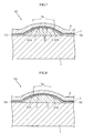
Fig. 1 is a sectional view showing a principal portion of a thermal printhead according to a first embodiment of the present invention. -
Fig. 2 is a plan view showing a principal portion of the thermal printhead according to the first embodiment. -
Fig. 3 is a sectional view showing the step of forming a glaze on a substrate in a method for manufacturing the thermal printhead according to the first embodiment. -
Fig. 4 is a sectional view showing the step of forming electrodes in the method for manufacturing the thermal printhead according to the first embodiment of the present invention. -
Fig. 5 is a sectional view showing the step of sinking the electrodes in the manufacturing method. -
Fig. 6 is a sectional view showing the step of forming an insulating film in the manufacturing method. -
Fig. 7 is a sectional view showing a principal portion of a thermal printhead according to a second embodiment of the present invention. -
Fig. 8 is a sectional view showing a principal portion of a thermal printhead according to a third embodiment of the present invention. -
Fig. 9 is a sectional view showing a principal portion of an example of conventional thermal printhead. - Preferred embodiments of the present invention will be described below with reference to the accompanying drawings.
Figs. 1 and 2 show a thermal printhead according to a first embodiment of the present invention. The illustrated thermal printhead A1 includes asubstrate 1, aglaze 2, a plurality offirst electrodes 3A, a plurality ofsecond electrodes 3B,insulating films 4,heating resistors 5 and aprotective film 6. For easier understanding, only theelectrodes insulating films 4 and theheating resistors 5 are shown inFig. 2 . - The
substrate 1 is a flat insulating plate which is in the form of an elongated rectangle extending in the primary scanning direction as viewed in plan and made of e.g. alumina ceramic material. Theglaze 2 is formed on thesubstrate 1 by printing and baking amorphous glass paste, for example. Theglaze 2 serves to retain heat and provide a smooth surface on which theelectrodes glaze 2 is elongated in the primary scanning direction and bulges in the thickness direction of thesubstrate 1 in cross section. Due to this shape, theglaze 2 enhances the contact pressure between a recording medium such as thermal paper and the portion of theprotective film 6 which covers theheating portion 5a, which will be described later. The maximum thickness of theglaze 2 is about 50 µm. - The first and the
second electrodes substrate 1 and theglaze 2 by e.g. printing and baking gold resinate paste. As shown inFig. 2 , thefirst electrode 3A and thesecond electrode 3B of each pair are spaced from each other in the secondary scanning direction, withrespective ends Fig. 1 , theends glaze 2, and the upper surfaces of theends ends electrodes - The insulating
films 4 are made of e.g. Ta2O5 and formed by baking Ta films formed by sputtering, for example. The insulatingfilms 4 cover the regions of theglaze 2 which are sandwiched between the pairedelectrodes films 4 partially overlaps theends film 4 extends in such a manner as to bridge the pairedelectrodes film 4 has a thickness of about 0.1 to 0.2 µm. The hardness of the insulatingfilm 4 is higher than that of theglaze 2 and lower than that of theheating resistors 5. The thermal conductivity of the insulatingfilm 4 is higher than that of theglaze 2 and lower than that of theheating resistors 5. The insulatingfilm 4 may be made of SiO2 instead of Ta2O5. - The
heating resistors 5 are formed on the insulatingfilms 4 in such a manner as to bridge theelectrodes heating resistors 5 are made of e.g. TaSiO2. Of eachheating resistor 5, the portion which is not in direct contact with theelectrodes heating portion 5a (see the diagonally shaded portion inFig. 2 ). When a voltage is applied across theelectrodes heating portion 5a generates heat. By utilizing this heat, the thermal printhead A1 performs printing on a recording medium such as thermal paper. In this embodiment, as shown inFig. 2 , the width of theheating resistor 5 is smaller than that of the insulatingfilm 4. Theheating resistor 5 has a thickness of 0.05 µm. - The
protective film 6 covers theglaze 2, theelectrodes films 4 and theheating resistors 5. Theprotective film 6 is formed by e.g. sputtering using SiC or SiAlON. Theprotective film 6 prevents theelectrodes heating resistors 5 from coming into direct contact with a recording medium or being affected chemically or electrically. Theprotective film 6 also serves to provide a smooth surface. The thickness of theprotective film 6 is about 4.0 µm. - A method for manufacturing the thermal printhead A1 will be described below with reference to
Figs. 3-6 . - First, as shown in
Fig. 3 , aglaze 2 is formed on asubstrate 1. This is performed by printing and baking amorphous glass paste. Specifically, on thesubstrate 1, glass paste is first printed in the form of a strip extending in the primary scanning direction. Then, the glass paste is baked. As a result, aglaze 2 is obtained which has a maximum thickness of about 50 µm and bulges in the thickness direction of thesubstrate 1 in cross section. - Then, as shown in
Fig. 4 ,electrodes substrate 1 andglaze 2. Specifically, first, gold resinate paste is printed in the form of a film on the upper surfaces of thesubstrate 1 andglaze 2, and then, the film is baked. Then, the baked paste film is subjected to patterning, wherebyelectrodes electrodes - As shown in
Fig. 5 , after theelectrodes ends electrodes glaze 2. This process can be achieved by softening theglaze 2 by heating. Specifically, theglaze 2 is heated at a temperature in the range from the glass softening point to the glass transition point of the glass component contained in theglaze 2. When theglaze 2 is softened, theends glaze 2 by their own weight. The amount of sinking can be adjusted by controlling the temperature or time of the heating. Thus, when the upper surfaces of theends glaze 2, theglaze 2 is caused to recover from the softened state. - Then, as shown in
Fig. 6 , insulatingfilms 4 are formed. First, to form the insulatingfilms 4, a film of Ta is formed by sputtering to bridge theends electrode pair film 4 made of Ta2O5 is obtained. The thickness of the insulatingfilm 4 is set to about 0.1 to 0.2 µm. The insulatingfilm 4 may be made of SiO2 instead of Ta2O5. - Thereafter,
heating resistors 5 covering the insulatingfilms 4 and bridging theelectrodes protective film 6 is formed to cover theelectrodes heating resistors 5. Thus, the thermal printhead A1 as shown inFigs. 1 and 2 is obtained. - The advantages of the thermal printhead A1 will be described below.
- According to the foregoing embodiment, a stepped portion is not provided between each of the
electrodes glaze 2. Further, owing to the existence of the insulatingfilms 4, theheating portions 5a are positioned close to a recording medium. As a result, the portions of theprotective film 6 which cover theheating portions 5a are pressed against a recording medium with a high pressure. Thus, the printing speed of the thermal printhead A1 can be increased. - Further, the heat from the
heating portions 5a is transferred to theglaze 2 via the insulatingfilms 4. Thus, the degree of increase or decrease of the heat theglaze 2 receives can be smaller. As a result, the thermal stress generated in theglaze 2 reduces, whereby theglaze 2 is prevented from cracking. Further, the insulatingfilms 4 function as a mechanical buffer between theglaze 2 and theheating resistors 5. Thus, the thermal expansion or contraction of the glaze 2 (which has a relatively low hardness) is prevented from being suppressed or promoted by the heating resistors 5 (which have a relatively high hardness). This is suitable for preventing theglaze 2 from cracking. - To make the insulating
films 4 have a hardness of a level between the hardness of theglaze 2 and that of theheating resistors 5 and a thermal conductivity of a level between the thermal conductivity of theglaze 2 and that of theheating resistors 5, it is preferable to form the insulatingfilms 4 using Ta2O5. In this embodiment, the region of theglaze 2 which is located between theelectrodes film 4. With this structure, theheating resistor 5 and theglaze 2 do not come into contact with each other, which is advantageous for preventing theglaze 2 from cracking. -
Figs. 7 and 8 show other embodiments of the present invention. In these figures, the elements which are identical or similar to those of the first embodiment are designated by the same reference signs as those used for the first embodiment. -
Fig. 7 shows a thermal printhead according to a second embodiment of the present invention. Unlike the first embodiment, the illustrated thermal printhead A2 includes adummy pattern 3C. Thedummy pattern 3C is made of e.g. Au and has a relatively high thermal conductivity. Thedummy pattern 3C comprises a plurality of elements spaced from each other in the secondary scanning direction. Thedummy pattern 3C is formed along with theelectrodes electrodes dummy pattern 3C is embedded in theglaze 2 and flush with theglaze 2. - With this arrangement, the heat from the
heating portions 5a is transferred well to theglaze 2 via thedummy pattern 3C. As a result, the variation in amount of heat transferred from theheating portions 5a to a recording medium is alleviated. When the amount of heat applied to the thermal paper varies largely, sticking of the thermal paper to theprotective film 6 is liable to occur. According to this embodiment, such sticking phenomenon is prevented. -
Fig. 8 shows a thermal printhead according to a third embodiment of the present invention. The illustrated thermal printhead A3 differs from the foregoing two embodiments in positional relationship among theglaze 2, theelectrodes films 4. In this embodiment, although theends electrodes glaze 2, the amount of sinking is smaller than the thickness of theends ends glaze 2. The level difference is substantially equal to the thickness of the insulatingfilm 4. The insulatingfilm 4 is located only between theelectrodes electrodes - According to this embodiment, a level difference is hardly defined between each of the
electrodes film 4. Thus, theheating resistor 5 is formed on a relatively smooth surface. By forming theheating resistor 5 on a smooth surface free from a level difference, theheating resistor 5 is prevented from having a non-uniform thickness and breaking due to e.g. the pressure applied in the printing process.
Claims (4)
- A thermal printhead comprising:a substrate;a glaze formed on the substrate and elongated in a primary scanning direction;a first and a second electrodes overlapping the glaze and spaced from each other in a secondary scanning direction;a heating resistor overlapping the first and the second electrodes and including a heat generating portion spaced apart from the electrodes; andan insulating film intervening between at least part of the heating portion of the heating resistor and the glaze;wherein at least an end of each of the electrodes is embedded in the glaze; andwherein the insulating film has a hardness which is higher than a hardness of the glaze and lower than a hardness of the heating resistor and a thermal conductivity which is higher than a thermal conductivity of the glaze and lower than a thermal conductivity of the heating resistor.
- The thermal printhead according to claim 1, wherein the insulating film bridges the first and the second electrodes.
- The thermal printhead according to claim 1, wherein the insulating film is made of either one of Ta2O5 and SiO2.
- A method for manufacturing a thermal printhead, the method comprising:forming a glaze elongated in a primary scanning direction on a substrate and forming a first and a second electrodes spaced from each other in a secondary scanning direction on the glaze;sinking at least an end of each of the electrodes into the glaze by softening at least part of the glaze by heating;forming an insulating film to cover at least part of a region of the glaze which is sandwiched between the first and the second electrodes; andforming a heating resistor to overlap the glaze and the first and the second electrodes in such a manner as to bridge the first and the second electrodes;wherein the insulating film is formed to have a hardness which is higher than a hardness of the glaze and lower than a hardness of the heating resistor and a thermal conductivity which is higher than a thermal conductivity of the glaze and lower than a thermal conductivity of the heating resistor.
Applications Claiming Priority (2)
| Application Number | Priority Date | Filing Date | Title |
|---|---|---|---|
| JP2006230495A JP2008049657A (en) | 2006-08-28 | 2006-08-28 | Thermal print head and its manufacturing method |
| PCT/JP2007/066529 WO2008026533A1 (en) | 2006-08-28 | 2007-08-27 | Thermal print head and method for manufacturing the same |
Publications (2)
| Publication Number | Publication Date |
|---|---|
| EP2058134A1 true EP2058134A1 (en) | 2009-05-13 |
| EP2058134A4 EP2058134A4 (en) | 2010-03-10 |
Family
ID=39135816
Family Applications (1)
| Application Number | Title | Priority Date | Filing Date |
|---|---|---|---|
| EP07793006A Withdrawn EP2058134A4 (en) | 2006-08-28 | 2007-08-27 | Thermal print head and method for manufacturing the same |
Country Status (4)
| Country | Link |
|---|---|
| US (1) | US7843475B2 (en) |
| EP (1) | EP2058134A4 (en) |
| JP (1) | JP2008049657A (en) |
| WO (1) | WO2008026533A1 (en) |
Families Citing this family (3)
| Publication number | Priority date | Publication date | Assignee | Title |
|---|---|---|---|---|
| KR101390153B1 (en) | 2011-12-22 | 2014-04-29 | 지멕주식회사 | Thermo-sensitive recording device and method of manufacturing a thermo-sensitive recording device |
| JP5972654B2 (en) * | 2012-04-27 | 2016-08-17 | ローム株式会社 | Thermal print head and method of manufacturing thermal print head |
| CN113386470A (en) * | 2020-03-11 | 2021-09-14 | 深圳市博思得科技发展有限公司 | Thermal print head and method of manufacturing the same |
Family Cites Families (26)
| Publication number | Priority date | Publication date | Assignee | Title |
|---|---|---|---|---|
| JPS60193667A (en) * | 1984-03-16 | 1985-10-02 | Yokogawa Hokushin Electric Corp | Thermal head and manufacture thereof |
| JPS6246657A (en) | 1985-08-23 | 1987-02-28 | Mitsubishi Electric Corp | Production of thermal head |
| JPS62169665A (en) * | 1986-01-22 | 1987-07-25 | Hitachi Metals Ltd | Membrane type thermal head |
| JPS62299348A (en) * | 1986-06-19 | 1987-12-26 | Tdk Corp | Heat generator for thermal head |
| JP2832977B2 (en) * | 1989-02-02 | 1998-12-09 | 富士ゼロックス株式会社 | Thermal head and method of manufacturing the same |
| US5066960A (en) * | 1989-04-05 | 1991-11-19 | Sharp | Thermal printing head |
| JP2519340B2 (en) * | 1990-05-10 | 1996-07-31 | シャープ株式会社 | Thermal recording device |
| US5252988A (en) | 1989-12-15 | 1993-10-12 | Sharp Kabushiki Kaisha | Thermal head for thermal recording machine |
| JPH04319446A (en) * | 1991-04-19 | 1992-11-10 | Oki Electric Ind Co Ltd | Thermal head |
| JPH04347662A (en) * | 1991-05-24 | 1992-12-02 | Kyocera Corp | Thermal head |
| JPH0542698A (en) * | 1991-08-10 | 1993-02-23 | Ricoh Co Ltd | Thermal head and preparation thereof |
| JPH0577462A (en) * | 1991-09-20 | 1993-03-30 | Ricoh Co Ltd | Thermal head and production thereof |
| JPH05131665A (en) * | 1991-11-13 | 1993-05-28 | Fuji Xerox Co Ltd | Thermal head |
| JP3069247B2 (en) | 1994-07-29 | 2000-07-24 | アルプス電気株式会社 | Thermal head |
| JPH08207333A (en) * | 1995-01-31 | 1996-08-13 | Kyocera Corp | Thermal head and manufacturing method thereof |
| JPH08207334A (en) * | 1995-02-06 | 1996-08-13 | Fuji Photo Film Co Ltd | Thermal head and its manufacture |
| JP3298780B2 (en) * | 1995-08-30 | 2002-07-08 | アルプス電気株式会社 | Thermal head and method of manufacturing thermal head |
| JP2793541B2 (en) * | 1995-12-28 | 1998-09-03 | ローム株式会社 | Thermal head |
| JPH1134374A (en) * | 1997-07-23 | 1999-02-09 | Tdk Corp | Thermal head and its manufacture |
| JPH1134376A (en) * | 1997-07-23 | 1999-02-09 | Tdk Corp | Thermal head and fabrication thereof |
| JP2001246770A (en) | 2000-03-04 | 2001-09-11 | Heiji Imai | Thermal print head and method of making the same |
| JP4319446B2 (en) | 2003-04-09 | 2009-08-26 | 株式会社岡村製作所 | Mirror support structure |
| JP2005047060A (en) * | 2003-07-30 | 2005-02-24 | Kyocera Corp | Thermal head, manufacturing method thereof, and thermal printer |
| JP4347662B2 (en) | 2003-11-05 | 2009-10-21 | 株式会社日立製作所 | Real-time control device |
| JP2005254506A (en) | 2004-03-09 | 2005-09-22 | Fuji Photo Film Co Ltd | Thermal head and thermal printer |
| EP1767374A4 (en) | 2004-05-25 | 2010-01-06 | Rohm Co Ltd | Thermal print head and method for manufacturing the same |
-
2006
- 2006-08-28 JP JP2006230495A patent/JP2008049657A/en active Pending
-
2007
- 2007-08-27 EP EP07793006A patent/EP2058134A4/en not_active Withdrawn
- 2007-08-27 WO PCT/JP2007/066529 patent/WO2008026533A1/en not_active Ceased
- 2007-08-27 US US12/438,859 patent/US7843475B2/en not_active Expired - Fee Related
Also Published As
| Publication number | Publication date |
|---|---|
| US20090201356A1 (en) | 2009-08-13 |
| EP2058134A4 (en) | 2010-03-10 |
| JP2008049657A (en) | 2008-03-06 |
| WO2008026533A1 (en) | 2008-03-06 |
| US7843475B2 (en) | 2010-11-30 |
Similar Documents
| Publication | Publication Date | Title |
|---|---|---|
| US7538785B2 (en) | Thermal print head and method for manufacturing the same | |
| US7843475B2 (en) | Thermal print head and method for manufacturing the same | |
| US7969458B2 (en) | Thermal printhead | |
| EP1815996A1 (en) | Thermal print head and method for manufacturing same | |
| JP4367771B2 (en) | Thermal head | |
| JP5322509B2 (en) | Thermal print head | |
| EP0829369B1 (en) | Thermal head and method of manufacturing the same | |
| JP3323960B2 (en) | Thin-film thermal printhead | |
| WO2005025877A1 (en) | Thermal printhead and method for manufacturing same | |
| US7876343B2 (en) | Thermal print head and method for manufacturing same | |
| JP2001232838A (en) | Thermal printing head and manufacturing method | |
| JP5990017B2 (en) | Thermal print head and manufacturing method thereof | |
| EP1077136A1 (en) | Thick-film thermal print head | |
| US6753893B1 (en) | Thermal head and method for manufacturing the same | |
| US8009185B2 (en) | Thermal head with protective layer | |
| JP2571865B2 (en) | Thick film type thermal head | |
| US7697020B2 (en) | Thermal print head and method for manufacturing same | |
| JP5670076B2 (en) | Thermal print head and manufacturing method thereof | |
| KR100888521B1 (en) | Thermal head and its manufacturing method | |
| CN113386469B (en) | Thermal print head and method of manufacturing the same | |
| JPH04347662A (en) | Thermal head | |
| CN113386470A (en) | Thermal print head and method of manufacturing the same | |
| JP3348927B2 (en) | Method of manufacturing thick film type thermal print head | |
| JP2001010098A (en) | Thermal head | |
| JPH09201994A (en) | Thermal head and its production |
Legal Events
| Date | Code | Title | Description |
|---|---|---|---|
| PUAI | Public reference made under article 153(3) epc to a published international application that has entered the european phase |
Free format text: ORIGINAL CODE: 0009012 |
|
| 17P | Request for examination filed |
Effective date: 20090310 |
|
| AK | Designated contracting states |
Kind code of ref document: A1 Designated state(s): AT BE BG CH CY CZ DE DK EE ES FI FR GB GR HU IE IS IT LI LT LU LV MC MT NL PL PT RO SE SI SK TR |
|
| AX | Request for extension of the european patent |
Extension state: AL BA HR MK RS |
|
| DAX | Request for extension of the european patent (deleted) | ||
| RBV | Designated contracting states (corrected) |
Designated state(s): DE FR GB |
|
| A4 | Supplementary search report drawn up and despatched |
Effective date: 20100208 |
|
| STAA | Information on the status of an ep patent application or granted ep patent |
Free format text: STATUS: THE APPLICATION IS DEEMED TO BE WITHDRAWN |
|
| 18D | Application deemed to be withdrawn |
Effective date: 20100508 |