EP2056286B1 - Liquid crystal display device - Google Patents
Liquid crystal display device Download PDFInfo
- Publication number
- EP2056286B1 EP2056286B1 EP07792475.1A EP07792475A EP2056286B1 EP 2056286 B1 EP2056286 B1 EP 2056286B1 EP 07792475 A EP07792475 A EP 07792475A EP 2056286 B1 EP2056286 B1 EP 2056286B1
- Authority
- EP
- European Patent Office
- Prior art keywords
- subpixel
- liquid crystal
- voltages
- subpixels
- storage capacitor
- Prior art date
- Legal status (The legal status is an assumption and is not a legal conclusion. Google has not performed a legal analysis and makes no representation as to the accuracy of the status listed.)
- Not-in-force
Links
Images


Classifications
-
- G—PHYSICS
- G09—EDUCATION; CRYPTOGRAPHY; DISPLAY; ADVERTISING; SEALS
- G09G—ARRANGEMENTS OR CIRCUITS FOR CONTROL OF INDICATING DEVICES USING STATIC MEANS TO PRESENT VARIABLE INFORMATION
- G09G3/00—Control arrangements or circuits, of interest only in connection with visual indicators other than cathode-ray tubes
- G09G3/20—Control arrangements or circuits, of interest only in connection with visual indicators other than cathode-ray tubes for presentation of an assembly of a number of characters, e.g. a page, by composing the assembly by combination of individual elements arranged in a matrix no fixed position being assigned to or needed to be assigned to the individual characters or partial characters
- G09G3/34—Control arrangements or circuits, of interest only in connection with visual indicators other than cathode-ray tubes for presentation of an assembly of a number of characters, e.g. a page, by composing the assembly by combination of individual elements arranged in a matrix no fixed position being assigned to or needed to be assigned to the individual characters or partial characters by control of light from an independent source
- G09G3/36—Control arrangements or circuits, of interest only in connection with visual indicators other than cathode-ray tubes for presentation of an assembly of a number of characters, e.g. a page, by composing the assembly by combination of individual elements arranged in a matrix no fixed position being assigned to or needed to be assigned to the individual characters or partial characters by control of light from an independent source using liquid crystals
- G09G3/3611—Control of matrices with row and column drivers
- G09G3/3614—Control of polarity reversal in general
-
- G—PHYSICS
- G09—EDUCATION; CRYPTOGRAPHY; DISPLAY; ADVERTISING; SEALS
- G09G—ARRANGEMENTS OR CIRCUITS FOR CONTROL OF INDICATING DEVICES USING STATIC MEANS TO PRESENT VARIABLE INFORMATION
- G09G3/00—Control arrangements or circuits, of interest only in connection with visual indicators other than cathode-ray tubes
- G09G3/20—Control arrangements or circuits, of interest only in connection with visual indicators other than cathode-ray tubes for presentation of an assembly of a number of characters, e.g. a page, by composing the assembly by combination of individual elements arranged in a matrix no fixed position being assigned to or needed to be assigned to the individual characters or partial characters
- G09G3/34—Control arrangements or circuits, of interest only in connection with visual indicators other than cathode-ray tubes for presentation of an assembly of a number of characters, e.g. a page, by composing the assembly by combination of individual elements arranged in a matrix no fixed position being assigned to or needed to be assigned to the individual characters or partial characters by control of light from an independent source
- G09G3/36—Control arrangements or circuits, of interest only in connection with visual indicators other than cathode-ray tubes for presentation of an assembly of a number of characters, e.g. a page, by composing the assembly by combination of individual elements arranged in a matrix no fixed position being assigned to or needed to be assigned to the individual characters or partial characters by control of light from an independent source using liquid crystals
- G09G3/3611—Control of matrices with row and column drivers
- G09G3/3648—Control of matrices with row and column drivers using an active matrix
- G09G3/3655—Details of drivers for counter electrodes, e.g. common electrodes for pixel capacitors or supplementary storage capacitors
-
- G—PHYSICS
- G09—EDUCATION; CRYPTOGRAPHY; DISPLAY; ADVERTISING; SEALS
- G09G—ARRANGEMENTS OR CIRCUITS FOR CONTROL OF INDICATING DEVICES USING STATIC MEANS TO PRESENT VARIABLE INFORMATION
- G09G2300/00—Aspects of the constitution of display devices
- G09G2300/04—Structural and physical details of display devices
- G09G2300/0421—Structural details of the set of electrodes
- G09G2300/0426—Layout of electrodes and connections
-
- G—PHYSICS
- G09—EDUCATION; CRYPTOGRAPHY; DISPLAY; ADVERTISING; SEALS
- G09G—ARRANGEMENTS OR CIRCUITS FOR CONTROL OF INDICATING DEVICES USING STATIC MEANS TO PRESENT VARIABLE INFORMATION
- G09G2300/00—Aspects of the constitution of display devices
- G09G2300/04—Structural and physical details of display devices
- G09G2300/0439—Pixel structures
- G09G2300/0443—Pixel structures with several sub-pixels for the same colour in a pixel, not specifically used to display gradations
-
- G—PHYSICS
- G09—EDUCATION; CRYPTOGRAPHY; DISPLAY; ADVERTISING; SEALS
- G09G—ARRANGEMENTS OR CIRCUITS FOR CONTROL OF INDICATING DEVICES USING STATIC MEANS TO PRESENT VARIABLE INFORMATION
- G09G2300/00—Aspects of the constitution of display devices
- G09G2300/08—Active matrix structure, i.e. with use of active elements, inclusive of non-linear two terminal elements, in the pixels together with light emitting or modulating elements
- G09G2300/0809—Several active elements per pixel in active matrix panels
- G09G2300/0842—Several active elements per pixel in active matrix panels forming a memory circuit, e.g. a dynamic memory with one capacitor
- G09G2300/0852—Several active elements per pixel in active matrix panels forming a memory circuit, e.g. a dynamic memory with one capacitor being a dynamic memory with more than one capacitor
-
- G—PHYSICS
- G09—EDUCATION; CRYPTOGRAPHY; DISPLAY; ADVERTISING; SEALS
- G09G—ARRANGEMENTS OR CIRCUITS FOR CONTROL OF INDICATING DEVICES USING STATIC MEANS TO PRESENT VARIABLE INFORMATION
- G09G2310/00—Command of the display device
- G09G2310/02—Addressing, scanning or driving the display screen or processing steps related thereto
- G09G2310/0262—The addressing of the pixel, in a display other than an active matrix LCD, involving the control of two or more scan electrodes or two or more data electrodes, e.g. pixel voltage dependent on signals of two data electrodes
-
- G—PHYSICS
- G09—EDUCATION; CRYPTOGRAPHY; DISPLAY; ADVERTISING; SEALS
- G09G—ARRANGEMENTS OR CIRCUITS FOR CONTROL OF INDICATING DEVICES USING STATIC MEANS TO PRESENT VARIABLE INFORMATION
- G09G2320/00—Control of display operating conditions
- G09G2320/06—Adjustment of display parameters
- G09G2320/0673—Adjustment of display parameters for control of gamma adjustment, e.g. selecting another gamma curve
-
- G—PHYSICS
- G09—EDUCATION; CRYPTOGRAPHY; DISPLAY; ADVERTISING; SEALS
- G09G—ARRANGEMENTS OR CIRCUITS FOR CONTROL OF INDICATING DEVICES USING STATIC MEANS TO PRESENT VARIABLE INFORMATION
- G09G2330/00—Aspects of power supply; Aspects of display protection and defect management
- G09G2330/04—Display protection
-
- G—PHYSICS
- G09—EDUCATION; CRYPTOGRAPHY; DISPLAY; ADVERTISING; SEALS
- G09G—ARRANGEMENTS OR CIRCUITS FOR CONTROL OF INDICATING DEVICES USING STATIC MEANS TO PRESENT VARIABLE INFORMATION
- G09G3/00—Control arrangements or circuits, of interest only in connection with visual indicators other than cathode-ray tubes
- G09G3/20—Control arrangements or circuits, of interest only in connection with visual indicators other than cathode-ray tubes for presentation of an assembly of a number of characters, e.g. a page, by composing the assembly by combination of individual elements arranged in a matrix no fixed position being assigned to or needed to be assigned to the individual characters or partial characters
- G09G3/34—Control arrangements or circuits, of interest only in connection with visual indicators other than cathode-ray tubes for presentation of an assembly of a number of characters, e.g. a page, by composing the assembly by combination of individual elements arranged in a matrix no fixed position being assigned to or needed to be assigned to the individual characters or partial characters by control of light from an independent source
- G09G3/3406—Control of illumination source
Definitions
- the present invention relates to a liquid crystal display device and more particularly relates to a liquid crystal display device that can reduce the viewing angle dependence of the ⁇ characteristic thereof.
- a liquid crystal display is a flat-panel display that has a number of advantageous features including high resolution, drastically reduced thickness and weight, and low power dissipation.
- the LCD market has been rapidly expanding recently as a result of tremendous improvements in its display performance, significant increases in its productivity, and a noticeable rise in its cost effectiveness over competing technologies.
- a twisted-nematic (TN) mode liquid crystal display device which used to be used extensively in the past, is subjected to an alignment treatment such that the major axes of its liquid crystal molecules, exhibiting positive dielectric anisotropy, are substantially parallel to the respective principal surfaces of upper and lower substrates and are twisted by about 90 degrees in the thickness direction of the liquid crystal layer between the upper and lower substrates.
- the liquid crystal molecules change their orientation directions into a direction that is parallel to the electric field applied.
- the TN mode liquid crystal display device utilizes variation in the optical rotatory characteristic of its liquid crystal layer due to the change of orientation directions of the liquid crystal molecules in response to the voltage applied, thereby controlling the quantity of light transmitted.
- the TN mode liquid crystal display device allows a broad enough manufacturing margin and achieves high productivity.
- the display performance e.g., the viewing angle characteristic, in particular
- the contrast ratio of the image decreases significantly.
- the grayscale characteristic of the image being displayed thereon may sometimes invert itself. That is to say, a portion of an image, which looks darker when viewed straight, may look brighter when viewed obliquely. This is a so-called "grayscale inversion phenomenon".
- an inplane switching (IPS) mode liquid crystal display device To improve the viewing angle characteristic of such a TN mode liquid crystal display device, an inplane switching (IPS) mode liquid crystal display device, a multi-domain vertical aligned (MVA) mode liquid crystal display device, an axisymmetric aligned (ASM) mode liquid crystal display device, and other types of liquid crystal display devices were developed recently.
- IPS inplane switching
- MVA multi-domain vertical aligned
- ASM axisymmetric aligned
- Liquid crystal displays employing any of the novel modes described above solve the concrete problems with viewing angle characteristics, specifically, the problems that the display contrast ratio decreases considerably or the grayscales invert when the display surface of the display is viewed obliquely.
- the ⁇ characteristic of LCDs would vary with the viewing angle. That is to say, the ⁇ characteristic when an image on the screen is viewed straight is different from the characteristic when it is viewed obliquely.
- the " ⁇ characteristic” refers to the grayscale .dependence of display luminance. That is why if the ⁇ characteristic when the image is viewed straight is different from the characteristic when the same image is viewed obliquely, then it means that the grayscale display state changes according to the viewing direction. This is a serious problem particularly when a still picture such as a photo is presented or when a TV program is displayed.
- such viewing angle dependence of the ⁇ characteristic can be reduced by providing two or more subpixels for each single pixel and by making the luminance of one of the two subpixels different from that of the other when a moderate luminance is displayed (see Patent Documents Nos. 1 and 2, for example).
- the liquid crystal display device disclosed in Patent Document No.1 applies a different effective voltage to the liquid crystal layer of a second subpixel from the one applied to the liquid crystal layer of a first subpixel when a moderate luminance is displayed, thereby making the luminances of the first and second subpixels different from each other and reducing the viewing angle dependence of the ⁇ characteristic.
- the transmittance of the liquid crystal layer changes with the absolute value of the effective voltage irrespective of the direction of the electric field applied to the liquid crystal layer (i.e., the direction of the electric line of force).
- the liquid crystal display device disclosed in Patent Document No. 1 inverts the direction of the electric field applied to the liquid crystal layer alternately every vertical scanning period, thereby flattening the uneven distribution of DC levels and overcoming residual image and other reliability-related problems.
- the liquid crystal display device disclosed in Patent Document No. 2 inverts the brightness levels of first and second subpixels every vertical scanning period (e.g., makes the luminance of the first subpixel higher than that of the second subpixel in a first vertical scanning period but makes the luminance of the second subpixel higher than that of the first subpixel in a second vertical scanning period).
- the device also inverts the direction of the electric field applied to the liquid crystal layer every vertical scanning period, too. If one of multiple subpixels were always bright, then the image on the screen would look non-smooth.
- the liquid crystal display device disclosed in Patent Document No. 2 minimizes such non-smoothness of the image on the screen by inverting the brightness levels of the first and second subpixels one vertical scanning period after another.
- multi-pixel display such a display or driving method that reduces the viewing angle dependence of the ⁇ characteristic by making the luminances of multiple subpixels different from each other
- a multi-pixel display a “multi-pixel drive”
- an "area grayscale display” or an “area grayscale drive” a display or driving method that reduces the viewing angle dependence of the ⁇ characteristic by making the luminances of multiple subpixels different from each other
- a liquid crystal display apparatus comprises a liquid crystal display panel with a liquid crystal layer and a plurality of electrodes for applying voltages to the liquid crystal layer as well as pixels each where the brightness varies in accordance with the display signal voltage received via a transistor.
- Each of the pixel comprises a first subpixel that exhibits a first brightness in response to an applied voltage as well as a second subpixel that exhibits a second brightness which is different from the first brightness corresponds to a respective applied voltage.
- a brightness switching circuit performs a switching of different modes so as to switch between a first mode with the larger brightness than the brightness of a second mode.
- the respective plurality of subpixels is arranged in particular patterns over a plurality of superordinate pixels.
- a liquid crystal display wherein the viewing-angle is increased by the use of a first gamma characteristics curve producing bright pixel values and a second gamma characteristics curve producing dark pixel values.
- the direction of the electric field applied to the liquid crystal layer and the brightness levels of the subpixels are inverted every vertical scanning period, the direction of the electric field applied to the liquid crystal layer is always the same when one of the two subpixels is brighter than the other subpixel.
- the electric field applied to the liquid crystal layer is directed from a subpixel electrode toward a counter electrode.
- the electric field with such a direction is supposed to have a first polarity.
- the electric field applied to the liquid crystal layer is directed from the counter electrode toward the subpixel electrode.
- the electric field with such a direction is supposed to have a second polarity.
- the electric field has the first polarity.
- the electric field has the second polarity.
- the electric field always has the first polarity when the effective voltage applied to the first subpixel has the greater absolute value and always has the second polarity when the effective voltage applied to the second subpixel has the greater absolute value. That is why the average effective voltages applied to the first and second subpixels have the first and second polarities, respectively.
- a normal liquid crystal display device In a normal liquid crystal display device, if the same image continues to be presented for a long time with the average of the voltages applied to a pixel kept unequal to zero (i.e., with a DC voltage component left in the voltage applied to the pixel), then that image that has been presented for a long time will still remain on the screen even when the images on the screen are changed after that. That is to say, a so-called "residual image" phenomenon will occur. To avoid such a residual image phenomenon, a normal liquid crystal display device performs an AC drive on (i.e., applies voltages with two different polarities but with the same absolute value to) pixels, thereby making the average of the voltages applied to the liquid crystal layer equal to zero. Furthermore, if the average of the voltages applied does not become equal to zero even by the AC drive, then the normal liquid crystal display device further regulates the counter voltage, thereby setting the average voltage equal to zero.
- the respective effective voltages applied to the first and second subpixels have mutually different averages. That is why even if the counter voltage is regulated, only the average voltage applied to one of the two subpixels can be made equal to zero and the average voltage applied to the other subpixel cannot be zero. In that case, the residual image phenomenon will occur in the subpixel with the non-zero average voltage. As a result, the residual image phenomenon cannot be eliminated from the overall display device. Consequently, in the liquid crystal display device disclosed in Patent Document No. 2, not both of the average voltages applied to the first and second subpixels can be equal to zero, and therefore, the residual image and other reliability-related problems should arise.
- the present invention has an object of providing a liquid crystal display device that can resolve those reliability-related problems such as non-smoothness of the image on the screen and the residual image phenomenon.
- a liquid crystal display device includes a plurality of pixels, each including a first subpixel and a second subpixel.
- Each of the first and second subpixels includes: a counter electrode; a subpixel electrode; and a liquid crystal layer interposed between the counter electrode and the subpixel electrode.
- the subpixel electrodes of the first and second subpixels are provided separately from each other as first and second subpixel electrodes, respectively, while the first and second subpixels share the same counter electrode with each other.
- the first and second subpixels When a predetermined grayscale tone is displayed continuously through four or more consecutive even number of vertical scanning periods, the first and second subpixels have mutually different luminances in at least two of the even number of vertical scanning periods, first polarity periods that are included in the even number of vertical scanning periods and that maintain a first polarity are as long as second polarity periods that are also included in the even number of vertical scanning periods and that maintain a second polarity for each of the first and second subpixels, and in each of the first and second polarity periods, the difference between the average of effective voltages applied to the liquid crystal layer of the first subpixel and that of effective voltages applied to the liquid crystal layer of the second subpixel is substantially equal to zero.
- the plurality of the pixels are arranged in column and row directions so as to form a matrix pattern, and in each of the plurality of the pixels, the first and second subpixels are arranged in the column direction.
- voltages applied to the first and second subpixel electrodes change as voltages on their associated storage capacitor lines vary.
- a voltage on a storage capacitor line associated with the first subpixel electrode and a voltage on a storage capacitor line associated with the second subpixel electrode change mutually differently.
- a voltage applied to the second subpixel electrode of a particular one of the plurality of the pixels and a voltage applied to the first subpixel electrode of another pixel that is adjacent to the particular pixel in the column direction change as the voltage on their common storage capacitor line varies.
- a voltage applied to the second subpixel electrode of a particular one of the plurality of the pixels and a voltage applied to the first subpixel electrode of another pixel that is adjacent to the particular pixel in the column direction change as voltages on their associated storage capacitor lines vary.
- the first and second subpixel electrodes are connected to the same signal line by way of their associated switching element.
- the first and second subpixel electrodes are respectively connected to first and second signal lines by way of first and second switching elements, respectively.
- the frame frequency is 60 Hz.
- the frame frequency is 120 Hz.
- the first and second subpixel electrodes have the same display area.
- the present invention provides a liquid crystal display device that can minimize the occurrence of reliability problems such as non-smoothness of image displayed or residual images.
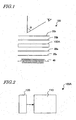
- FIG. 1 illustrates the liquid crystal display device 100 .
- the liquid crystal panel 100A of the liquid crystal display device 100 includes a display section 110 in which a number of pixels are arranged in columns and rows to define a matrix pattern and a driver 120 for driving the display section 110 as shown in FIG. 2 .
- each pixel includes a liquid crystal layer and a plurality of electrodes for applying a voltage to the liquid crystal layer.
- the driver 120 generates a drive signal based on an input video signal.
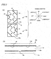
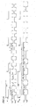
- FIG. 3(a) is a schematic plan view illustrating the electrode structure of a single pixel
- FIG. 3(b) is a schematic cross-sectional view of a single subpixel as viewed on the plane 3B-3B' shown in FIG. 3(a)
- each pixel 10 includes first and second subpixels 10a and 10b that are arranged in the column direction.
- the first subpixel 10a includes a liquid crystal layer 13, a first subpixel electrode 18a, and a counter electrode 17 that faces the first subpixel electrode 18a with the liquid crystal layer 13 interposed between them.
- 3(b) illustrates the configuration of only the first subpixel 10a
- the second subpixel 10b has the same configuration as the one illustrated in FIG. 3(b)
- the counter electrode 17 is typically provided as a single common electrode for every pixel 10.
- mutually different voltages are applicable to the first and second subpixel electrodes 18a and 18b, thus making the effective voltage applied to the liquid crystal layer of the first subpixel 10a different from the one applied to that of the second subpixel 10b.
- each pixel is supposed to display a predetermined grayscale tone for several frames on end for the sake of simplicity.
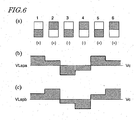
- the reference numerals 1 through 6 denote respective vertical scanning periods.
- one "vertical scanning period" is defined to be an interval between a point in time when one scan line is selected to write a display signal voltage and a point in time when that scan line is selected to write the next display signal voltage.
- each of one frame period of a non-interlaced drive input video signal and one field period of an interlaced drive input video signal will be referred to herein as "one vertical scanning period of the input video signal".
- one vertical scanning period of a liquid crystal display device corresponds to one vertical scanning period of the input video signal.
- one vertical scanning period of the liquid crystal panel is supposed to correspond to that of the input video signal for the sake of simplicity.
- the present invention is in no way limited to that specific preferred embodiment.
- the present invention is also applicable to a so-called "2x drive" with a vertical scanning frequency of 120 Hz in which two vertical scanning periods of the liquid crystal panel (that lasts 2 ⁇ 1/120 sec, for example) are allocated to one vertical scanning period of the input video signal (that lasts 1/60 sec, for example). Also, in this example, the lengths of the respective vertical scanning periods are supposed to be equal to each other. Furthermore, in each vertical scanning period, the interval between a point in time when one scan line is selected and a point in time when the next scan line is selected will be referred to herein as one horizontal scanning period (1H).
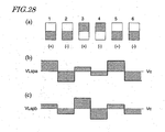
- the upper and lower rectangles represent the first and second subpixels, respectively. Of these two subpixels, the one with the higher luminance is plain, while the other with the lower luminance is shadowed.
- "+" and "-” represent the polarities of the display signal voltages when the associated scan line is selected with respect to the common voltage applied to the counter electrode. In this case, "+” indicates that the potential at the first and second subpixel electrodes is higher than the one at the counter electrode and that the electric field is directed from the subpixel electrodes toward the counter electrode.
- "-" indicates that the potential at the first and second subpixel electrodes is lower than the one at the counter electrode and that the electric field is directed from the counter electrode toward the subpixel electrodes.
- “+” and “-” will be referred to herein as a “first polarity” and a “second polarity”, respectively, and will also be collectively referred to herein as “polarities”.
- a period with the "+” polarity and a period with the "-” polarity will be referred to herein as a "first polarity period” and a “second polarity period”, respectively.
- the first, third and fifth periods are first polarity periods
- the second, fourth and sixth periods are second polarity periods
- the polarity inverts every vertical scanning period in the liquid crystal display device disclosed in Patent Document No. 1.
- the first subpixel in any of the first through sixth periods, has a higher luminance than the second subpixel in the device of Patent Document No. 1.
- Portions (b) and (c) of FIG. 4 show the effective voltages VLspa and VLspb that are applied to the respective liquid crystal layers of the first and second subpixels in the respective vertical scanning periods in the liquid crystal display device of Patent Document No. 1. The levels of these voltages are indicated by the bold lines.
- the effective voltages VLspa and VLspb applied to the respective liquid crystal layers of the first and second subpixels are the effective values of the differences between the voltages applied to the first and second subpixel electrodes and the voltage Vc applied to the counter electrode.
- the voltage Vc applied to the counter electrode is shown as being constant.
- the voltages applied to the respective liquid crystal layers of the first and second subpixels may also be changed within the same vertical scanning period by varying the voltage on the storage capacitor line as disclosed in Patent Document No. 1.
- the voltages applied to the first and second subpixel electrodes are higher than the voltage applied to the counter electrode, and the absolute value of the effective voltage applied to the liquid crystal layer of the first subpixel is greater than that of the effective voltage applied to that of the second subpixel (
- the first period is a first polarity period and the first subpixel is brighter than the second subpixel.
- the effective voltages VLspa and VLspb applied to the respective liquid crystal layers of the first and second subpixels change.
- the voltages applied to the first and second subpixel electrodes are lower than the voltage applied to the counter electrode, and the absolute value of the effective voltage applied to the liquid crystal layer of the first subpixel is greater than that of the effective voltage applied to that of the second subpixel (
- the second period is a second polarity period and the first subpixel is brighter than the second subpixel.
- the first, third and fifth periods are also first polarity periods
- the second, fourth and sixth periods are second polarity periods
- the luminance of the first subpixel is higher than that of the second subpixel in the first, third and fifth periods but the luminance of the second subpixel is higher than that of the first subpixel in the second, fourth and sixth periods.
- Portions (b) and (c) of FIG. 5 show the effective voltages VLspa and VLspb that are applied to the respective liquid crystal layers of the first and second subpixels in the respective vertical scanning periods. The levels of these voltages are indicated by the bold lines. Although not shown in portions (b) and (c) of FIG. 5 , the voltages applied to the respective liquid Crystal layers of the first and second subpixels may also be changed within the same vertical scanning period by varying the voltage on the storage capacitor line as disclosed in Patent Document No. 1.
- the voltages applied to the first and second subpixel electrodes are higher than the voltage applied to the counter electrode, and the absolute value of the effective voltage applied to the liquid crystal layer of the first subpixel is greater than that of the effective voltage applied to that of the second subpixel (
- the first period is a first polarity period and the first subpixel is brighter than the second subpixel.
- the effective voltages VLspa and VLspb applied to the respective liquid crystal layers of the first and second subpixels change.
- the voltages applied to the first and second subpixel electrodes are lower than the voltage applied to the counter electrode, and the absolute value of the effective voltage applied to the liquid crystal layer of the second subpixel is greater than that of the effective voltage applied to that of the first subpixel (
- the second period is a second polarity period and the second subpixel is brighter than the first subpixel.
- the first subpixel is sometimes brighter, but sometimes less bright, than the second subpixel unlike the liquid crystal display device disclosed in Patent Document No. 1. Consequently, the degree of non-smoothness on the screen can be reduced.
- the period in which the first subpixel is brighter than the second subpixel is always the first polarity period and the period in which the second subpixel is brighter than the first subpixel is always the second polarity period.
- the average of the effective voltages VLspa applied to the liquid crystal layer of the first subpixel over multiple vertical scanning periods is higher than the voltage Vc applied to the counter electrode
- the average of the effective voltages VLspb applied to the liquid crystal layer of the second subpixel over multiple vertical scanning periods is lower than the voltage Vc applied to the counter electrode.
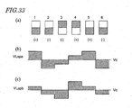
- the first, second, fifth and sixth periods are first polarity periods, while the third and fourth periods are second polarity periods.
- the first polarity period is a period in which the voltages applied to the first and second subpixel electrodes are higher than the one applied to the counter electrode
- the second polarity period is a period in which the voltages applied to the first and second subpixel electrodes are lower than the one applied to the counter electrode.
- two out of the four periods are first polarity periods and the other two are second polarity periods.
- the first and second periods are first polarity periods and the third and fourth periods are second polarity periods.
- Portions (b) and (c) of FIG. 6 show the effective voltages VLspa and VLspb that are applied to the respective liquid crystal layers of the first and second subpixels in the respective vertical scanning periods. The levels of these voltages are indicated by the bold lines.
- the voltages applied to the respective liquid crystal layers of the first and second subpixels may also be changed within the same vertical scanning period by varying the voltage on the storage capacitor line just as disclosed in Patent Documents Nos. 1 and 2.
- the voltage Vc applied to the counter electrode is used as a reference voltage in portions (b) and (c) of FIG. 6 , the voltage Vc applied to the counter electrode is illustrated as being constant irrespective of time. However, the voltage Vc applied to the counter electrode may also vary with time.
- the voltages applied to the first and second subpixel electrodes are higher than the voltage applied to the counter electrode, and the absolute value of the effective voltage applied to the liquid crystal layer of the first subpixel is greater than that of the effective voltage applied to that of the second subpixel (
- the first period is a first polarity period and the first subpixel is brighter than the second subpixel.
- the effective voltages VLspa and VLspb applied to the respective liquid crystal layers of the first and second subpixels change.
- the voltages applied to the first and second subpixel electrodes are higher than the voltage applied to the counter electrode, and the absolute value of the effective voltage applied to the liquid crystal layer of the second subpixel is greater than that of the effective voltage applied to that of the first subpixel (
- the second period is a first polarity period and the second subpixel is brighter than the first subpixel.
- the voltages applied to the first and second subpixel electrodes are lower than the voltage applied to the counter electrode, and the absolute value of the effective voltage applied to the liquid crystal layer of the first subpixel is greater than that of the effective voltage applied to that of the second subpixel (
- the third period is a second polarity period and the first subpixel is brighter than the second subpixel.
- the fourth period the voltages applied to the first and second subpixel electrodes are lower than the voltage applied to the counter electrode, and the absolute value of the effective voltage applied to the liquid crystal layer of the second subpixel is greater than that of the effective voltage applied to that of the first subpixel (
- the fourth period is a second polarity period and the second subpixel is brighter than the first subpixel.
- two out of four consecutive vertical scanning periods are first polarity periods, one of which satisfies
- the two other ones of the four consecutive vertical scanning periods are second polarity periods, one of which satisfies
- the brightness levels of the subpixels are inverted every vertical scahning period and the polarity is inverted every other vertical scanning period.
- the (brightness, polarity) combination of the first subpixel changes in the order of (B(right), +), (D(ark), +), (B, -) and (D, -)
- the (brightness, polarity) combination of the second subpixel changes in the order of (D +), (B, +), (D, -) and (B, -)
- “B” indicates that the pixel is brighter than the other pixel
- "D" indicates that the pixel is darker than the other.
- the difference between the average of the effective voltage applied to the liquid crystal layer of the first subpixel and that of the effective voltages applied to that of the second subpixel in each of the first and second polarity periods becomes substantially equal to zero.
- the liquid crystal display device 100 of this preferred embodiment inverts the brightness levels of the subpixels every vertical scanning period, thus minimizing the degree of non-smoothness of the image on the screen.
- each pair of first and second polarity periods has a period that satisfies
- the average of the effective voltages VLspa and that of the effective voltages VLspb over multiple vertical scanning periods can be both equal to zero. Furthermore, even if the averages of the effective voltages VLspa and VLspb do not become equal to zero, the averages of the effective voltages VLspa and VLspb can be both controlled to zero by adjusting the counter voltage because the average of the effective voltages VLspa is approximately equal to that of the effective voltages VLspb. By controlling the averages of the effective voltages to zero in this manner, the residual image and other reliability-related problems can be overcome. It should be noted that various configurations could be used to apply mutually different voltages to the respective liquid crystal layers of the first and second subpixels such that the relations described above are satisfied.
- This first example is preferably applied to a liquid crystal display device that uses a vertical alignment liquid crystal layer including a nematic liquid crystal material with negative dielectric anisotropy.
- the liquid crystal layer of each subpixel preferably has four domains in which the liquid crystal molecules tilt in respective azimuth directions that are different from each other by approximately 90 degrees under a voltage applied (i.e., may operate in the MVA mode).
- the liquid crystal layer of each subpixel may also have axisymmetric alignment at least when a voltage is applied thereto (i.e., may operate in the ASM mode).
- the liquid crystal display device 100 includes a liquid crystal panel 100A, a pair of phase compensators (typically phase plates) 20a and 20b arranged on both sides of the liquid crystal panel 100A, a pair of polarizers 30a and 30b arranged to sandwich these members between them, and a backlight 40.
- the polarizers 30a and 30b are arranged as crossed Nicols such that their axes of transmission (which will also be referred to herein as "axes of polarization”) cross each other at right angles. While no voltage is applied to the liquid crystal layer 13 of the liquid crystal panel 100A (see FIG. 3(b) ), i.e., in a vertical alignment state, this device conducts black display.
- this liquid crystal display device 100 is a normally black mode liquid crystal display device.
- the phase compensators 20a and 20b are provided to improve the viewing angle characteristic of the liquid crystal display device and may be designed as best ones by known technologies. Specifically, the phase compensators 20a and 20b may be optimized such that the difference in luminance between when the image is viewed obliquely and when the image is viewed straight in the black display mode (i.e., the difference in black luminance) is minimized in every azimuth direction.
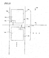
- a scan line 12 is arranged between the first and second subpixel electrodes 18a and 18b.
- scan lines 12, signal lines, TFTs (not shown in FIG. 3 ) and circuits for driving them are arranged on the substrate 11a to apply predetermined voltages to the first and second subpixel electrodes 18a and 18b at prescribed timings.
- color filters and other members are arranged as needed.
- the subpixel electrode 18a on the glass substrate 11a has a slit 18s, and the subpixel electrode 18a and the counter electrode 17 together generate an oblique electric field in the liquid crystal layer 13.
- the liquid crystal layer 13 On the other hand, on the surface of the glass substrate 11b with the counter electrode 17, arranged are ribs 19 that protrude toward the liquid crystal layer 13, which is made of a nematic liquid crystal material with negative dielectric anisotropy.
- the liquid crystal layer 13 exhibits a substantially vertically aligned state when no voltages are applied thereto. That is to say, the vertically aligned liquid crystal molecules can be tilted toward a predetermined direction with stability by using the sloped side surfaces of the ribs 19 and the oblique electric field in combination.
- the ribs 19 have sloped side surfaces that are raised toward their center, and the liquid crystal molecules are aligned substantially perpendicularly to those tilted side surfaces. Consequently, the ribs 19 produce a distribution of tilt angles of the liquid crystal molecules.
- the tilt angle of a liquid crystal molecule means the angle defined by the long axis of the molecules with respect to the surface of the substrate.
- the slit 18s changes the directions of the electric field applied to the liquid crystal layer regularly. Due to the combined effects of these ribs 19 and the slit 18s, when an electric field is applied, the liquid crystal molecules are aligned in the four directions indicated by the arrows in FIG.
- the rectangular display area of the liquid crystal panel 100A is typically arranged such that its longitudinal direction is defined horizontally and the transmission axis of the polarizer 30a is defined to be parallel to the longitudinal direction.
- the pixels 10 are arranged such that the longitudinal direction of the pixels 10 intersects with that of the liquid crystal panel 100A at right angles.
- the first and second subpixels 10a and 10b preferably have the same area.
- Each of these subpixels preferably has a first rib that runs in a first direction and a second rib that runs in a second direction that intersects with the first direction substantially at right angles, and the first and second ribs are preferably arranged symmetrically to each other within each subpixel with respect to a centerline that is defined parallel to the scan line 12 .
- the arrangement of the ribs in one of the two subpixels and that of the ribs in the other subpixel are preferably symmetrical to each other with respect to a centerline that is drawn perpendicularly to the scan line 12 .
- the liquid crystal molecules are aligned upper rightward, upper leftward, lower rightward and lower leftward within each subpixel and the respective liquid crystal domains come to have substantially the same area in the entire pixel including the first and second subpixels.
- a good viewing angle characteristic that is symmetrical both vertically and horizontally is realized. This effect is achieved particularly significantly when a pixel has a small area.
- it is preferred to adopt a configuration in which the interval between the respective centerlines of the two subpixels that are drawn parallel to the scan line is approximately equal to a half of the arrangement pitch of the scan lines.
- each pixel 10 in the liquid crystal display device 100 will be described with reference to FIGS. 7 through 9 .
- the pixel 10 includes two subpixels 10a and 10b.
- the gate electrodes of the TFTs 16a and 16b are both connected to the same scan line 12 .
- the source electrodes of the TFTs 16a and 16b are connected to the same signal line 14 .
- the storage capacitors 22a and 22b are connected to their associated storage capacitor lines (CS bus lines) 24a and 24b , respectively.
- the storage capacitor 22a includes a storage capacitor electrode that is electrically connected to the subpixel electrode 18a , a storage capacitor counter electrode that is electrically connected to the storage capacitor line 24a , and an insulating layer (not shown) arranged between the electrodes.
- the storage capacitor 22b includes a storage capacitor electrode that is electrically connected to the subpixel electrode 18b , a storage capacitor counter electrode that is electrically connected to the storage capacitor line 24b , and an insulating layer (not shown) arranged between the electrodes.
- the respective storage capacitor counter electrodes of the storage capacitors 22a and 22b are independent of each other and can receive mutually different storage capacitor counter voltages from the storage capacitor lines 24a and 24b , respectively.
- FIG. 8 schematically shows the equivalent circuit of one pixel 10 of the liquid crystal display device 100.
- the liquid crystal layers of the subpixels 10a and 10b are identified by the reference numerals 13a and 13b , respectively.
- a liquid crystal capacitor formed of the subpixel electrode 18a , the liquid crystal layer 13a , and the counter electrode 17 will be identified by Clca.
- a liquid crystal capacitor formed of the subpixel electrode 18b , the liquid crystal layer 13b , and the counter electrode 17 will be identified by Clcb.
- the same counter electrode 17 is shared by these two subpixels 10a and 10b.
- the liquid crystal capacitors Clca and Clcb are supposed to have the same electrostatic capacitance CLC (V).
- CLC CLC
- V the effective voltages (V) applied to the liquid crystal layers of the respective subpixels 10a and 10b.
- the storage capacitors 22a and 22b that are connected independently of each other to the liquid crystal capacitors of the respective subpixels 10a and 10b will be identified herein by Ccsa and Ccsb, respectively, which are supposed to have the same electrostatic capacitance CCS .
- one electrode of the liquid crystal capacitor Clca and one electrode of the storage capacitor Ccsa are connected to the drain electrode of the TFT 16a , which functions as a switching element for the subpixel 10a.
- the other electrode of the liquid crystal capacitor Clca is connected to the counter electrode 17 .
- the other electrode of the storage capacitor Ccsa is connected to the storage capacitor line 24a .
- one electrode of the liquid crystal capacitor Clcb and one electrode of the storage capacitor Ccsb are connected to the drain electrode of the TFT 16b , which functions as a switching element for the subpixel 10b.
- the other electrode of the liquid crystal capacitor Clcb is connected to the counter electrode 17 .
- the other electrode of the storage capacitor Ccsb is connected to the storage capacitor line 24b .
- the gate electrodes of the TFTs 16a and 16b are both connected to the scan line 12 and the source electrodes thereof are both connected to the signal line 14 .
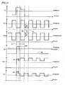
- FIG. 9 schematically shows how the respective voltages that are applied to drive the liquid crystal display device 100 vary within a vertical scanning period.
- Vs represents the voltage on the signal line 14 ;
- Vcsa represents the voltage on the storage capacitor line 24a ;
- Vcsb represents the voltage on the storage capacitor line 24b ;
- Vg represents the voltage on the scan line 12 ;
- Vlca represents the voltage to the first subpixel electrode 18a ;
- Vlcb represents the voltage to the second subpixel electrode 18b .
- the dashed line indicates the voltage COMMON (Vc) to the counter electrode 17 .
- the voltage Vcsa on the storage capacitor line 24a varies periodically within the range of Vc - Vad to Vc + Vad.
- the voltage Vcsb on the storage capacitor line 24b also varies periodically within the range of Vc-Vad to Vc+ Vad.
- the waveform of the voltage Vcsb on the storage capacitor line 24b has a phase that is different by 180 degrees from that of the voltage Vcsa on the storage capacitor line 24a .
- the voltage Vg on the scan line 12 rises from VgL to VgH to turn the TFTs 16a and 16b ON simultaneously.
- the voltage Vs on the signal line 14 is transmitted to the subpixel electrodes 18a and 18b of the subpixels 10a and 10b to charge the liquid crystal capacitors Clca and Clcb of the subpixels 10a and 10b.
- the storage capacitors Csa and Csb of the respective subpixels are also charged with the voltage on the signal line 14 .
- the voltage Vg on the scan line 12 falls from VgH to VgL to turn the TFTs 16a and 16b OFF simultaneously and electrically isolate the liquid crystal capacitors Clca and Clcb of the subpixels 10a and 10b and the storage capacitors Ccsa and Ccsb from the signal line 14 .
- Vlca Vs - Vd + 2 ⁇ K ⁇ Vad
- the voltage Vcsa on the storage capacitor line 24a falls from Vc+Vad to Vc-Vad and the voltage Vcsb on the storage capacitor line 24b rises from Vc-Vad to Vc+Vad. That is to say, these voltages Vcsa and Vcsb both change twice as much as Vad again.
- the voltage Vcsa on the storage capacitor line 24a rises from Vc-Vad to Vc+Vad and the voltage Vcsb on the storage capacitor line 24b falls from Vc +Vad to Vc-Vad. That is to say, these voltages Vcsa and Vcsb both change twice as much as Vad again.
- Vlcb Vs - Vd - 2 ⁇ K ⁇ Vad respectively.
- the voltages Vcsa , Vcsb, Vlca and Vlcb alternate their levels at the times T4 and T5 .
- the alternation interval between T4 and T5 may be appropriately determined to be one, two, three or more times as long as 1H according to the driving method of the liquid crystal display device (such as the polarity inversion method) or the display state (such as the degree of flicker or non-smoothness of the image displayed).
- V ⁇ 1 Vs - Vd + K ⁇ Vad - Vc
- V ⁇ 2 Vs - Vd - K ⁇ Vad - Vc respectively.
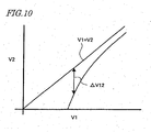
- FIG. 10 schematically shows the relation between V1 and V2 in the liquid crystal display device 100 .
- the smaller the V1 value the bigger ⁇ v in the liquid crystal display device 100 of this preferred embodiment.
- the ⁇ v value varies with V1 or V2 because the static capacitance CLC(V) of the liquid crystal capacitor varies with the voltage.
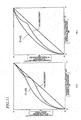
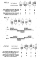
- FIG. 11(a) shows the ⁇ characteristic of the liquid crystal display device 100 at a right 60 degree viewing angle
- FIG. 11(b) shows the ⁇ characteristic of the liquid crystal display device 100 of this preferred embodiment at an upper right 60 degree viewing angle
- FIGS. 11(a) and 11(b) also show the ⁇ characteristics that were observed when the same voltage was applied to the subpixels 10a and 10b for the purpose of comparison.
- the ⁇ characteristic is improved by this preferred embodiment.
- the respective voltages as shown in FIG. 9 by varying the respective voltages as shown in FIG. 9 within a single vertical scanning period, mutually different effective voltages are applicable to the respective liquid crystal layers of different subpixels, and the ⁇ characteristic in an oblique viewing direction is improved as a result.
- Vg represents the voltage on the scan line 12
- Vcsa and Vcsb represent the voltages on the first and second storage capacitor lines 24a and 24b , respectively
- VLspa and VLspb represent the effective voltages applied to the respective liquid crystal layers 13a and 13b of the first and second subpixel electrodes 10a and 10b.
- one vertical scanning period is an interval between a point in time when a scan line is selected and a point in time when the next scan line is selected, and is represented by V-Total in FIG. 12 . It should be noted that the variation in the voltage Vd caused by the feedthrough phenomenon that has already been described with reference to FIG. 9 is not shown in FIG. 12 .
- the voltages Vcsa and Vcsb on the first and second storage capacitor lines each have display periods AH and regulation periods BH.
- Each of these voltages Vcsa and Vcsb on the first and second storage capacitor lines varies periodically in different cycles through the display and regulation periods AH and BH.
- the voltages Vcsa and Vcsb vary in regular cycles of 20H through the display periods AH and in different regular cycles of either 36H or 26H through the regulation periods BH.
- the sum of one display period AH and one regulation period BH is equal to one vertical scanning period (V-Total).
- the display period AH begins when the voltages Vcsa and Vcsb on the first and second storage capacitor lines change after a vertical scanning period for a certain frame has started.
- the regulation period BH ends when the voltages Vcsa and Vcsb on the first and second storage capacitor lines change after the vertical scanning period for that frame has terminated.
- the frame frequency may be 60 Hz, for example.
- FIG. 12 shows how the voltages change through four vertical scanning periods.
- those four vertical scanning periods will be referred to herein as first, second, third and fourth vertical scanning periods, respectively
- the display periods AH and regulation periods BH associated with those vertical scanning periods will be referred to herein as first, second, third and fourth display periods AH and first, second, third and fourth regulation periods BH , respectively.
- the voltage Vcsa on the storage capacitor line 24a rises to a higher voltage VcH
- the voltage Vcsb on the storage capacitor line 24b falls to a lower voltage VcL.
- Vcsb rises to a higher voltage VcH .
- the difference between VcH and VcL is equal to 2 ⁇ Vad that has already been described with reference to FIG. 9 .
- the voltage Vg on the scan line 12 changes from VgL into VgH.
- the first vertical scanning period begins and the first and second subpixel electrodes 18a and 18b are charged.
- the voltage Vg on the scan line 12 is VgH
- the voltage Vs on the signal line 14 is higher than the voltage Vc at the counter electrode 17 . That is why as a result of the charge, the voltages at the first and second subpixel electrodes 18a and 18b become higher than the voltage Vc at the counter electrode 17 .
- the first and second subpixel electrodes 18a and 18b finish being charged.
- the voltage Vcsa on the first storage capacitor line 24a rises to VcH and the voltage Vcsb on the second storage capacitor line 24b falls to VcL.
- the first display period AH it is when the voltage Vcsa on the first storage capacitor line 24a increases and the voltage Vcsb on the second storage capacitor line 24b decreases that the first display period AH begins.
- the voltages Vcsa and Vcsb on the first and second storage capacitor lines 24a and 24b increase or decrease every 10H period and vary periodically in regular cycles of 20H.
- the first regulation period BH begins.
- the voltages Vcsa and Vcsb on the first and second storage capacitor lines 24a and 24b increase or decrease every 18H period.
- the voltages at the first and second subpixel electrodes 18a and 18b change as the voltages Vcsa and Vcsb on the first and second storage capacitor lines 24a and 24b vary. That is why in the first vertical scanning period, the absolute value of the effective voltage applied to the liquid crystal layer 13a of the first subpixel 10a becomes greater than that of the effective voltage applied to the liquid crystal layer 13b of the second subpixel 10b and the first subpixel 10a becomes brighter than the second subpixel 10b.
- the voltage Vg on the scan line 12 changes from VgL into VgH.
- the first vertical scanning period ends and the second vertical scanning period begins and the first and second subpixel electrodes 18a and 18b are charged. While the voltage Vg on the scan line 12 is VgH, the voltage Vs on the signal line 14 is higher than the voltage Vc at the counter electrode 17 .
- the voltages at the first and second subpixel electrodes 18a and 18b become higher than the voltage Vc at the counter electrode 17 . Thereafter, when the voltage Vg on the scan line 12 falls from VgH to VgL again, the first and second subpixel electrodes 18a and 18b finish being charged.
- the voltage Vcsa on the first storage capacitor line 24a falls to VcL and the voltage Vcsb on the second storage capacitor line 24b rises to VcH.
- the voltage Vcsa on the first storage capacitor line 24a decreases and the voltage Vcsb on the second storage capacitor line 24b increases that the first regulation period ends and the second display period AH begins.
- the voltages Vcsa and Vcsb on the first and second storage capacitor lines 24a and 24b also increase or decrease every 10H period and vary periodically in regular cycles of 20H.
- the voltages Vcsa and Vcsb on the first and second storage capacitor lines 24a and 24b will increase or decrease every 13H period.
- the voltages at the first and second subpixel electrodes 18a and 18b change as the voltages Vcsa and Vcsb on the first and second storage capacitor lines 24a and 24b vary. That is why in the second vertical scanning period, the absolute value of the effective voltage applied to the liquid crystal layer 13b of the second subpixel 10b becomes greater than that of the effective voltage applied to the liquid crystal layer 13a of the first subpixel 10a and the second subpixel 10b becomes brighter than the first subpixel 10a.
- the voltage Vg on the scan line 12 changes from VgL into VgH.
- the second vertical scanning period ends and the third vertical scanning period begins and the first and second subpixel electrodes 18a and 18b are charged. While the voltage Vg on the scan line 12 is VgH, the voltage Vs on the signal line 14 is lower than the voltage Vc at the counter electrode 17 .
- the voltages at the first and second subpixel electrodes 18a and 18b become lower than the voltage Vc at the counter electrode 17. Thereafter, when the voltage Vg on the scan line 12 falls from VgH to VgL again, the first and second subpixel electrodes 18a and 18b finish being charged.
- the voltage Vcsa on the first storage capacitor line 24a falls to VcL and the voltage Vcsb on the second storage capacitor line 24b rises to VcH.
- the second regulation period BH ends and the third display period AH begins.
- the voltages Vcsa and Vcsb on the first and second storage capacitor lines 24a and 24b also increase or decrease every 10H period and vary periodically in regular cycles of 20H.
- the voltages Vcsa and Vcsb on the first and second storage capacitor lines 24a and 24b will increase or decrease every 18H period.
- the voltages at the first and second subpixel electrodes 18a and 18b change as the voltages Vcsa and Vcsb on the first and second storage capacitor lines 24a and 24b vary. That is why in the third vertical scanning period, the absolute value of the effective voltage applied to the liquid crystal layer 13a of the first subpixel 10a becomes greater than that of the effective voltage applied to the liquid crystal layer 13b of the second subpixel 10b and the first subpixel 10a becomes brighter than the second subpixel 10b.
- the voltage Vg on the scan line 12 changes from VgL into VgH.
- the third vertical scanning period ends and the fourth vertical scanning period begins and the first and second subpixel electrodes 18a and 18b are charged. While the voltage Vg on the scan line 12 is VgH, the voltage Vs on the signal line 14 is lower than the voltage Vc at the counter electrode 17 .
- the voltages at the first and second subpixel electrodes 18a and 18b become lower than the voltage Vc at the counter electrode 17 . Thereafter, when the voltage Vg on the scan line 12 falls from VgH to VgL again, the first and second subpixel electrodes 18a and 18b finish being charged.
- the voltage Vcsa on the first storage capacitor line 24a rises to VcH and the voltage Vcsb on the second storage capacitor line 24b falls to VcL.
- the voltage Vcsa on the first storage capacitor line 24a increases and the voltage Vcsb on the second storage capacitor line 24b decreases that the third regulation period BH ends and the fourth display period AH begins.
- the voltages Vcsa and Vcsb on the first and second storage capacitor lines 24a and 24b also increase or decrease every 10H period and vary periodically in regular cycles of 20H.
- the voltages Vcsa and Vcsb on the first and second storage capacitor lines 24a and 24b will increase or decrease every 13H period.
- the voltages at the first and second subpixel electrodes 18a and 18b change as the voltages Vcsa and Vcsb on the first and second storage capacitor lines 24a and 24b vary. That is why in the fourth vertical scanning period, the absolute value of the effective voltage applied to the liquid crystal layer 13b of the second subpixel 10b becomes greater than that of the effective voltage applied to the liquid crystal layer 13a of the first subpixel 10a and the second subpixel 10b becomes brighter than the first subpixel 10a. From the fifth vertical scanning period on, the respective voltages will vary in quite the same way as in the first through fourth vertical scanning periods shown in FIG. 12 .
- the (brightness, polarity) combination of the first subpixel changes in the order of (B, +), (D, +), (B, -) and (D, -), while the (brightness, polarity) combination of the second subpixel changes in the order of (D, +), (B, +), (D, -) and (B, -). That is to say, the brightness levels and polarities of the first and second subpixels change just as shown in portion (a) of FIG. 6 .
- the voltages Vcsa and Vcsb on the first and second storage capacitor lines in this manner, the deterioration of display quality can be minimized in a liquid crystal display device, of which the r characteristic has reduced viewing angle dependence.
- the liquid crystal display device is designed such that the potentials at the pixel electrode and at the counter electrode switch their levels at regular intervals and that the direction of the electric field applied to the liquid crystal layer is also inverted at regular intervals.
- the directions of the electric field applied to the liquid crystal layer change from toward the light source side into toward the viewer side, and vice versa.
- Such a drive method that sets an alternating current voltage is called an "AC drive method”.
- the inversion interval of the direction of the electric field applied to the liquid crystal layer may be 66.667 ms, which is twice as long as two frame periods of 33.333 ms, for example.
- the direction of the electric field applied to the liquid crystal layer is inverted every time two frame pictures are presented. That is why in presenting a still picture, unless the electric field strengths (i.e., the magnitudes of applied voltages) exactly matched with each other in respective electric field directions (i.e., if the electric field intensities changed every time the directions of the electric field change), the pixel luminances would change and a flicker would be produced on the screen whenever the electric field intensities change.
- the electric field strengths i.e., the magnitudes of applied voltages
- the electric field intensities (or the magnitudes of applied voltages) in the respective electric field directions need to be exactly matched with each other.
- the flicker is reduced by arranging pixels with mutually different electric field directions adjacent to each other within a display area and spatially averaging the luminances of those pixels.
- Such a method is generally called either a "dot inversion” or a "line inversion”.
- inversion drive methods that include not just a method in which the polarities of those pixels are inverted in a checkered pattern on a pixel-by-pixel basis (i.e., the polarities are inverted both every row and every column, which is a so-called “dot inversion drive”) and a method in which the polarities are inverted on a line-by-line basis (i.e., the polarities are inverted every row, which is a so-called “line inversion drive”) but also a method in which the polarities are inverted every other row and every column (which is a so-called “two-row, one-column dot inversion drive”). And an appropriate one of those methods is selected as needed.
- the absolute values of the effective voltages applied to the liquid crystal layer should agree with each other as closely as possible. That is to say, as in resolving the reliability-related problem described above, the average of the voltages applied to the liquid crystal layer should be as close to zero as possible.
- pixels among which the electric field is applied to the liquid crystal layer in respectively different directions in each frame period, should be arranged adjacent to each other.
- a third condition is that one type of subpixels that are brighter than subpixels of the other type be arranged as randomly as possible within the same frame.
- those subpixels are preferably arranged such that the one type of subpixels, which are brighter than the subpixels of the other type, are adjacent to each other in neither the column direction nor the row direction.
- the one type of subpixels that are brighter than the other type are preferably arranged in a checkered pattern.
- the liquid crystal display device 100 has a pixel arrangement that can be used effectively to get the one-dot inversion drive done with those conditions satisfied.
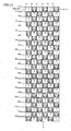
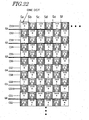
- FIG. 13 illustrates an equivalent circuit of the liquid crystal display device 100 .
- each pixel is supposed to have the structure shown in FIGS. 7 and 8 . Those pixels are arranged in a matrix pattern.
- pixel n-m a pixel located at an n th row and an m th column
- subpixel n-m-A subpixel n-m-A
- subpixel n-m-B subpixel n-m-B
- the liquid crystal display device 100 includes ten storage capacitor trunks CS1 through CS10 , and each subpixel is connected to one of those storage capacitor trunks CS1 through CS10 by way of a storage capacitor line (CS bus line).
- CS bus line a storage capacitor line
- the storage capacitor trunk CS2 is connected to subpixels 1-a-B, 1-b-B, 1-c-B, etc. on the first pixel row and to subpixels 2-a-A , 2-b-A, 2-c-A, etc. on the second pixel row.
- each subpixel and another subpixel included in a different pixel that is adjacent to the former subpixel are connected to the same storage capacitor trunk by way of the same storage capacitor line.
- the first and second subpixels 1-a-A and 1-a-B include liquid crystal capacitors CLC1-a-A and CLC1-a-B and storage capacitors CCS1-a-A and CCS1-a-B, respectively.
- Each of the liquid crystal capacitors is formed by a subpixel electrode, the counter electrode ComLC and the liquid crystal layer interposed between them.
- Each of the storage capacitors is formed by a storage capacitor electrode, an insulating film and a storage capacitor counter electrode ComCS1 or ComCS2.
- the first and second subpixels 1-a-A and 1-a-B are connected in common to the same signal line Sa by way of their associated TFTs 1-a-A and 1-a-B, respectively.
- the TFTs 1-a-A and 1-a-B have their ON/OFF states controlled with a voltage supplied onto their common signal line G1. And when these two TFTs are ON, voltages are applied through the same signal line Sa to the respective subpixel electrodes and respective storage capacitor electrodes of the first and second subpixels 1-a-A and 1-a-B.
- the storage capacitor counter electrode of the subpixel 1-a-A is connected to the storage capacitor trunk CS1 by way of its associated storage capacitor line (CS bus line) CS1 .
- the storage capacitor counter electrode of the subpixel 1-a-B is connected to the storage capacitor trunk CS2 by way of its associated storage capacitor line (CS bus line) CS2 .
- CS bus line storage capacitor line
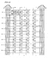
- FIG. 14 shows the brightness levels and polarities of respective subpixels that have changed within the effective scanning period of a certain frame. Specifically, in FIG. 14 , illustrated are pixels on the first through twelfth rows and the a th through f th columns.
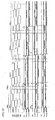
- FIG. 15 shows the waveforms of respective voltages (or signals) to drive a liquid crystal display device with the configuration shown in FIG. 13 . In FIG.
- Vsa and Vsb represent the voltages on the signal lines Sa and Sb
- Vg1 through Vg12 represent the voltages on the scan lines G1 through G12
- Vcs1 through Vcs10 represent the voltages on the storage capacitor trunks CS1 through CS10
- VLsp1-a-A through VLsp2-b-B represent the effective voltages applied to the liquid crystal layer of associated subpixels, respectively.
- What is shown in FIG. 15 is voltage waveforms within one vertical scanning period.
- the liquid crystal display device with the configuration shown in FIG. 13 is driven with voltages having the waveforms shown in FIG. 15 .
- every pixel is supposed to display the same grayscale tone to avoid complicating the description excessively.
- the voltages Vsa and Vsb on the signal lines Sa and Sb oscillate in regular cycles and with a predetermined amplitude as shown in FIG. 15 .
- One cycle time of oscillation of these voltages Vsa and Vsb is two horizontal scanning periods (2H).
- the voltage Vsb on the signal line Sb varies with a phase difference of 180 degrees with respect to the voltage Vsa on the signal line Sa.
- a period in which the voltage Vsa or Vsb is higher than the voltage at the counter electrode is identified by "+” and a period in which the former is lower than the latter is identified by "-”.
- a voltage on a signal line is transmitted to a subpixel electrode by way of one of the TFTs and then changes due to a variation in the voltage Vg on a scan line, thus producing a feedthrough phenomenon.
- the voltage at the counter electrode is determined in view of this feedthrough phenomenon. Also, although not shown in FIG.
- the voltages on other signal lines Sc and Se also vary in the same way as the voltage Vsa on the signal line Sa and the voltages on other signal lines Sd and Sf also vary in the same way as the voltage Vsb on the signal line Sb. Furthermore, as described above, an interval between a point in time when a voltage Vg on a certain scan line rises from Low level (VgL) to High level (VgH) and a point in time when the voltage Vg on the next scan line rises from VgL to VgH is one horizontal scanning period (1H).
- the voltages Vcs1 through Vcs10 on the storage capacitor trunks CS1 through CS10 oscillate with the same amplitude and in the same regular cycles.
- one oscillation cycle time is 20 H.
- the voltages Vcs1 and Vcs2 have such a relation that if one of these two voltages changes into VcH, the other voltage will change into VcL and that if one of these two voltages changes into VcL, the other voltage will change into VcH.
- the other four pairs of voltages Vcs3 and Vcs4 , Vcs5 and Vcs6 , Vcs7 and Vcs8 , and Vcs9 and Vcs10 too have the same relation as that pair of voltages Vcs1 and Vcs2 .
- the voltages Vcs3 and Vcs4 change 2H after the voltages Vcs1 and Vcs2 have changed. In the same way, there is a time lag of 2H between the changes of the voltages Vcs5 and Vcs6, the voltages Vcs7 and Vcs8 and the voltages Vcs9 and Vcs10 .
- the voltages at the subpixels 1-a-A and 1-a-B change as an example.
- the liquid crystal capacitors CLC1-a-A and CLC1-a-B of the subpixels 1-a-A and 1-a-B are charged. If the voltage Vg1 on the scan line G1 is VgH, the voltage Vsa on the signal line Sa is positive "+” and the liquid crystal capacitors CLC1-a-A and CLC1-a-B of the subpixels 1-a-A and 1-a-B are charged to a higher potential level than the one at the counter electrode.
- the absolute value of the effective voltage applied to the liquid crystal layer of the subpixel 1-a-A that is electrically connected to the storage capacitor trunk CS1 becomes greater than that of the effective voltage applied to that of the subpixel 1-a-B that is electrically connected to the storage capacitor trunk CS2 .
- the effective voltage applied to the liquid crystal layer of that subpixel becomes higher than the voltage on its associated signal line when the voltage on its associated scan line is VgH.
- the effective voltage applied to the liquid crystal layer of that subpixel becomes lower than the voltage on its associated signal line when the voltage on its associated scan line is VgH.
- FIG. 14 shows the brightness levels and polarities of subpixels that have changed during the effective scanning period of a certain frame.
- the sign "B" indicates that the given subpixel is brighter than the other subpixel (i.e., the absolute value of the effective voltage applied to the liquid crystal layer of that subpixel is greater than that of the effective voltage applied to the liquid crystal layer of the other).
- the sign "D" indicates that the given subpixel is darker than the other subpixel (i.e., the absolute value of the effective voltage applied to the liquid crystal layer of that subpixel is smaller than that of the effective voltage applied to that of the other).
- the sign "+” also indicates that the voltage at the subpixel electrode is higher than the one at the counter electrode and the sign "-" also indicates that the voltage at the subpixel electrode is lower than the one at the counter electrode.
- Two subpixels included in each pixel are adjacent to a pixel with a smaller row number and a pixel with a bigger row number. In this example, of the two subpixels included in a single pixel, the subpixel adjacent to the pixel with the smaller row number will be identified herein by "A” and the subpixel adjacent to the pixel with the bigger row number will be identified herein by "B".
- the brightness levels and polarities of the subpixels 1-a-A and 1-a-B included in the pixel 1-a will be described.
- the voltage Vg1 on the scan line G1 is VgH
- the voltage Vsa on the signal line Sa is higher than the voltage at the counter electrode. Therefore, the polarities of the subpixels 1-a-A and 1-a-B are both positive "+”.
- the voltages Vcs1 and Vcs2 on the storage capacitor trunks CS1 and CS2 associated with the respective subpixels are as indicated by the leftmost arrows in FIG. 15 .
- the brightness levels and polarities of subpixels 1-b-A and 1-b-B included in the pixel 1-b will be described. While the voltage Vg1 on the scan line G1 is VgH, the voltage Vsb on the signal line Sb is lower than the voltage at the counter electrode. Thus, the polarities of the subpixels 1-b-A and 1-b-B are both negative "-". On the other hand, when the voltage Vg1 on the scan line G1 changes from VgH into VgL, the voltages Vcs1 and Vcs2 on the storage capacitor trunks CS1 and CS2 associated with the respective subpixels 1-b-A and 1-b-B are as indicated by the leftmost arrows in FIG. 15 . That is why as can be seen from FIG.
- the brightness levels and polarities of subpixels 2-b-A and 2-b-B included in the pixel 2-b will be described.
- the voltage Vg2 on the scan line G2 is VgH
- the voltage Vsb on the signal line Sb is higher than the voltage at the counter electrode.
- the polarities of the subpixels 2-b-A and 2-b-B are both positive "+”.
- the voltages Vcs2 and Vcs3 on the storage capacitor trunks CS2 and CS3 associated with the respective subpixels 2-b-A and 2-b-B are as indicated by the second leftmost arrows in FIG. 15 .
- the liquid crystal display device satisfies the three conditions mentioned above.
- the liquid crystal display device satisfies the first condition for the following reasons.
- the liquid crystal display device satisfies the first condition, i.e., the absolute values of the effective voltages applied to the liquid crystal layers of respective subpixels agree with each other in respective electric field directions.
- the first condition i.e., the absolute values of the effective voltages applied to the liquid crystal layers of respective subpixels agree with each other in respective electric field directions.
- each pixel includes two subpixels, of which the liquid crystal layers are supplied with mutually different effective voltages.
- the brighter subpixel i.e., the subpixel marked "B" in FIG. 14
- this first condition is imposed on the subpixels marked "B", in particular.
- the first condition will be discussed with reference to the respective voltage waveforms shown in FIG. 15 , which shows the voltages VLsp1-a-A and VLsp2-a-A to be applied to the liquid crystal layers of the "B" subpixels 1-a-A and 2-a-A with mutually different electric field directions (or polarities).
- the solid line represents the voltages applied to the subpixel electrodes of the subpixels 1-a-A and 2-a-A
- the dashed line represents the voltage applied to the counter electrode.
- the effective voltage applied to the liquid crystal layer is a difference between the voltages represented by the solid and dashed lines. That is why if the effective voltages applied to the liquid crystal layer in respective electric field directions (or the quantities of charge stored in the liquid crystal capacitors) are matched with each other as closely as possible by appropriately defining the voltage applied to the counter electrode, the first condition can be satisfied.
- the liquid crystal display device satisfies the second condition, i.e., pixels with mutually different polarities are arranged adjacent to each other in each frame period.
- each pixel includes two subpixels, of which the liquid crystal layers are supplied with different effective voltages. That is why this second condition is imposed on not only on each pixel but also subpixels with the same effective voltage as well.
- this second condition is particularly important for bright subpixels, i.e., the subpixels marked "B" in FIG. 14 , to satisfy this second condition as in the first condition described above.
- the signs "+” and "-" representing the polarities (or electric field directions) of respective subpixels are inverted every other pixel (i.e., every second column) in the row direction (i.e., in the horizontal direction) in the order of (+, -), (+, -), (+, -), and so on, and also inverted every other pixel (i.e., every second row) in the column direction (i.e., in the vertical direction) in the order of (+, -), (+, -), (+, -), (+, -), and so on. That is to say, looking on a pixel-by-pixel basis, this device achieves the so-called “dot inversion" state, and therefore, satisfies the second condition.
- the bright subpixels i.e., the subpixels marked "B” in FIG. 14
- the bright subpixels i.e., the subpixels marked "B” in FIG. 14
- the polarity of every "B" subpixel is positive "+”.
- the device satisfies the third condition.
- multiple subpixels of which the luminance levels are intentionally different from each other, should be arranged such that subpixels with the same luminance level are adjacent to each other at as small a number of locations as possible.
- FIG. 14 looking at a total of four subpixels that are arranged on two rows and two columns (e.g., the subpixels 1-a-A, 1-a-B , 1-b-A and 1-b-B ), it can be seen that "B" and "D” subpixels are arranged in this order along the first column and then "D" and "B” subpixels are arranged in this order along the next column.
- the liquid crystal display device that has just been described with reference to FIGS. 14 and 15 satisfies all of the three conditions mentioned above, and therefore, realizes a display of quality images with a flicker eliminated.
- FIGS. 14 and 15 The brightness levels and polarities of subpixels that have changed within the effective scanning period of a certain frame and the voltage waveforms are shown in FIGS. 14 and 15 .
- the voltages on the signal lines change according to the waveforms shown in FIG. 15 with respect to the voltages on the scan lines but the voltages on the storage capacitor trunks change inversely to the waveforms shown in FIG. 15 . That is why in that frame, the polarities of the respective subpixels are the same as those of the subpixels shown in FIG. 14 but the brightness levels of the respective subpixels are inverted compared to the counterparts shown in FIG. 14 .
- Vcs1 through Vcs6 represent the voltages on the storage capacitor trunks CS1 through CS6
- Vg1 through Vg3 represent the voltages on the scan lines G1 through G3
- VLsp1-a-A through VLsp3-a-B represent the effective voltages applied to the respective liquid crystal layers of the subpixels 1-a-A through 3-a-B.
- the four consecutive frames will be identified herein by n, n+1, n+2 and n+3, respectively.
- FIG. 16 also shows vertical scanning periods of an input video signal.
- Each vertical scanning period of the input video signal consists of an effective scanning period V- Disp during which pixels in the liquid crystal panel 100A (see FIG. 1 ) are selected on a row-by-row basis and a vertical-blanking interval V-Blank during which no pixels in the liquid crystal panel 100A are selected at all.
- the duration of the effective scanning period is determined by the display area (or the number of rows of effective pixels) of the liquid crystal panel 100A .
- the “vertical scanning period” refers to a “vertical scanning period of a liquid crystal panel”. That is to say, a “vertical scanning period” (i.e., a “vertical scanning period of the liquid crystal panel”) is used herein in a different sense from a “vertical scanning period of an input video signal".
- a “vertical scanning period of an input video signal” is either a one-frame period or a one-field period, which begins and ends simultaneously for every pixel.
- a “vertical scanning period” means an interval between a point in time when a scan line is selected to write a display signal voltage and a point in time when that scan line is selected to write the next display signal voltage as described above.
- the vertical scanning periods start at different timing and end at different timing according to the associated scan line.
- the oblique lines indicate that the start and end times of a vertical scanning period change according to the row of pixels selected.
- scan lines are sequentially selected one after another from the first one.
- a voltage applied to its associated subpixel electrode changes to start a vertical scanning period for that subpixel.
- one vertical scanning period of an input video signal consists of an effective scanning period V-Disp and a vertical-blanking interval V- Blank .
- the vertical scanning period of a certain subpixel begins in the middle of the effective scanning period of a frame n, continues through the vertical-blanking interval, and then ends halfway through the effective scanning period of the next frame n+1. After that, when its associated scan line is selected next time, the next vertical scanning period will begin for that subpixel.
- the length of the "vertical scanning period" is equal to that of the "vertical scanning period of the input video signal”.
- the (brightness, polarity) combinations of the subpixel 1-a-A change in the order of (B, +), (D, +), (B, -), and (D, - ); the (brightness, polarity) combinations of the subpixel 1- a-B change in the order of (D, +), (B, +), (D, -), and (B, -); the (brightness, polarity) combinations of the subpixel 2-a-A change in the order of (B, -), (D, -), (B, +), and (D, +); and the (brightness, polarity) combinations of the subpixel 2-a-B change in the order of (D, -), (B, -), (D, +), and (B, +).
- FIG. 17 shows the brightness levels and polarities of the subpixels 1-a-A and 1-a-B and the first change of voltages on the storage capacitor lines at the vertical scanning period of the subpixels 1-a-A and 1-a-B.
- the polarity of the subpixels 1-a-A and 1-a-B is positive "+”
- the first change of voltages on the storage capacitor line at the vertical scanning period of the subpixel 1-a-A is increase " ⁇ ”
- the first change of voltages on the storage capacitor line at the vertical scanning period of the subpixel 1-a-B is decrease " ⁇ ".
- the polarity of the subpixels 1-a-A and 1-a-B is positive "+"
- the first change of voltages on the storage capacitor line at the vertical scanning period of the subpixel 1-a-A is decrease " ⁇ ”
- the first change of voltages on the storage capacitor line at the vertical scanning period of the subpixel 1-a-B is increase " ⁇ ".
- the polarity of the subpixels 1-a-A and 1-a-B is negative "-"
- the first change of voltages on the storage capacitor line at the vertical scanning period of the subpixel 1-a-A is decrease " ⁇ ”
- the first change of voltages on the storage capacitor line at the vertical scanning period of the subpixel 1-a-B is increase " ⁇ ”.
- the polarity of the subpixels 1-a-A and 1-a-B is negative "-"
- the first change of voltages on the storage capacitor line at the vertical scanning period of the subpixel 1-a-A is increase " ⁇ ”
- the first change of voltages on the storage capacitor line at the vertical scanning period of the subpixel 1-a-B is decrease " ⁇ ".
- the (polarity, first change of voltages on storage capacitor line) combinations of the subpixel 1-a-A from frame n through frame n+3 change (+, ⁇ ), (+, ⁇ ), (-, ⁇ ) and (-, ⁇ ) in this order. That is to say, mutually different combinations appear one after another.
- the (polarity, first change of voltages on storage capacitor line) combinations of the subpixel 1-a-B from frame n through frame n+3 change (+, ⁇ ), (+, ⁇ ), (-, ⁇ ) and (-, ⁇ ) in this order. That is to say, these combinations of the subpixel 1-a-B have the same polarity change pattern as, but a different storage capacitor line voltage variation pattern from, those of the subpixel 1-a-A.
- the voltage on each storage capacitor line is supposed to change periodically in regular cycles of 20H during the display period.
- the voltage on each storage capacitor line may also change in regular cycles of 16H during the display period as shown in portion (a) of FIG. 18 .
- the storage capacitor line voltage changes every 13H in the first and third regulation periods BH but changes every 9H in the second and fourth regulation periods BH , for example.
- the storage capacitor line voltage may also change in regular cycles of 24H during the display period as shown in portion (b) of FIG. 18 .
- the storage capacitor line voltage changes every 15H in the first and third regulation periods BH but changes every 21H in the second and fourth regulation periods BH , for example.
- the intervals of the variation in storage capacitor line voltage during the BH period may be appropriately changed according to the V-total value.
- each storage capacitor line is supposed to complete one cycle of change during each regulation period.
- the voltage on each storage capacitor line may also change periodically during each regulation period either in a cycle time of 2H as shown in portion (a) of FIG. 19 or in a cycle time of 1H as shown in portion (b) of FIG. 19 .
- the voltage on each storage capacitor line may also be maintained at the average of VcH and VcL during each regulation period as shown in portion (c) of FIG. 19 .
- each vertical scanning period has a duration of 810H and the storage capacitor voltages Vcs1 through Vcs3 change periodically in regular cycles of 20H during the display period but changes every 5H during the regulation period.
- a half-cycle period may be provided as a regulation period for the storage capacitor line voltage and the polarity may be inverted every other vertical scanning period. Then, as already described with reference to FIG. 17 , the first change of storage capacitor voltages at the beginning of the third vertical scanning period can be different from the first change of storage capacitor voltages at the beginning of the first vertical scanning period. As a result, the brightness levels and polarities of subpixels can be changed as shown in portion (a) of FIG. 6 .
- each regulation period is supposed to be an even number of times as long as one horizontal scanning period.
- Each regulation period may also be an odd number of times as long as one horizontal scanning period. Even if the first and third regulation periods have a cycle time of 37H and if the second and fourth regulation periods have a cycle time of 27H as shown in FIG. 21 , the degree of non-smoothness of the image on the screen can also be reduced by inverting the brightness levels and polarities of respective subpixels as in a situation where each regulation period is an even number of times as long as one horizontal scanning period.
- the same storage capacitor line is supposed to be connected to two subpixels belonging to two different adjacent pixels.
- the present invention is in no way limited to that specific description. Two different storage capacitor lines may also be provided for two subpixels belonging to two different adjacent pixels and the voltages on those two storage capacitor lines may be changed independently of each other.
- FIG. 22 shows the brightness levels and polarities of respective subpixels that have changed within the effective scanning period of a certain frame. Specifically, in FIG. 22 , illustrated are pixels on the first through sixth rows and the a th through f th columns.
- the liquid crystal display device 100 also has ten storage capacitor trunks CS1 through CS10 .
- the storage capacitor trunk CS1 is connected to subpixels 1-a-A, 1-b-A, 1-c-A, etc. on the first row of pixels and to subpixels 6-a-A, 6-b-A, 6-c-A , etc. on the sixth row of pixels.
- the storage capacitor trunk CS2 is connected to subpixels 1-a-B, 1-b-B, 1-c-B, etc.
- FIG. 23 illustrates an equivalent circuit of the liquid crystal display device 100 with the configuration shown in FIG. 22 .
- FIG. 24 shows the waveforms of various voltages (or signals) to drive the liquid crystal display device.
- Vsa and Vsb represent the voltages on the signal lines Sa and Sb
- Vg1 through Vg12 represent the voltages on the scan lines G1 through G12
- Vcs1 through Vcs10 represent the voltages on the storage capacitor trunks CS1 through CS10
- VLsp1-a-A through VLsp2-b-B represent the effective voltages applied to the liquid crystal layers of the subpixels 1-a-A through 2-b-B , respectively.
- What is shown in FIG. 24 is voltage waveforms within one vertical scanning period.
- the voltages Vcs1 through Vcs10 on the storage capacitor trunks CS1 through CS10 oscillate with the same amplitude and in the same regular cycles.
- one oscillation cycle time is 10 H.
- the voltages Vcs1 and Vcs2 have such a relation that if one of these two voltages changes into VcH, the other voltage will change into VcL and that if one of these two voltages changes into VcL, the other voltage will change into VcH.
- the other four pairs of voltages Vcs3 and Vcs4 , Vcs5 and Vcs6, Vcs7 and Vcs8, and Vcs9 and Vcs10 too have the same relation as that pair of voltages Vcs1 and Vcs2 .
- the voltage Vcs1 increases ( ⁇ ) and the voltage Vcs2 decreases ( ⁇ ).
- the voltage Vcs3 decreases ( ⁇ ) and the voltage Vcs4 increases ( ⁇ ).
- the liquid crystal display device with the configuration shown in FIG. 22 can also reduce the viewing angle dependence of the ⁇ characteristic and minimize the deterioration of display quality.
- a single signal line 14 is provided as a common line for two subpixels 10a and 10b included in the same pixel 10 as shown in FIG. 8 .
- the present invention is in no way limited to that specific description. Two different signal lines may also be provided for two subpixels included in the same pixel. In that case, even if the voltages on storage capacitor lines are not changed subpixel by subpixel, mutually different effective voltages can also be applied to the liquid crystal layers of subpixels by varying the voltages on the signal lines.
- FIG. 25 illustrates a pixel 10 , of which the two subpixels 10a and 10b are provided with signal lines 14a and 14b , respectively.
- the pixel 10 includes two subpixel electrodes 18a and 18b that are connected to the two different signal lines 14a and 14b via their associated TFTs 16a and 16b, respectively.
- the TFTs 16a and 16b have their gates connected to the same scan line (i.e., gate bus line) 12 in common and have their ON/OFF states controlled using the same scan signal.
- signal voltages are supplied to the signal lines (i.e., source bus lines) 14a and 14b so as to satisfy the relation described above. It is preferred that the gates of the TFTs 16a and 16b be used in common.
- the voltage applied to the counter electrode is shown to be constant. However, the present invention is in no way limited to that specific description.
- the voltage applied to the counter electrode may be changed with time.
- FIG. 10 shows that the effective voltages applied to the first and second subpixels are different from each other in a broad grayscale range.
- the effective voltages applied to the subpixels could be different from each other only in a particular grayscale range (e.g., in the range of 36 th through 128 th grayscales in a 256 grayscale display in which the grayscale range from black to white is divided into 256 levels consisting of 0 th through 255 th grayscales).
- a normally black mode liquid crystal display device e.g., an MVA mode LCD, among other things. If necessary, this is also applicable for use in an IPS mode liquid crystal display device.
- the viewing angle dependence of the ⁇ characteristic is more significant in the MVA and ASM modes than in the IPS mode. In the IPS mode, however, it is more difficult to manufacture panels that can have a high contrast ratio in the frontal viewing direction than in the MVA and ASM modes. In view of these considerations, it can be seen that it is a more urgent task to overcome the viewing angle dependence problem of the r characteristic of the MVA and ASM mode liquid crystal display devices.
- liquid crystal display device 100 of this second example is different from the counterpart of the first example described above in the brightness levels and polarities of subpixels and the order of change of the effective voltages in the four consecutive vertical scanning periods.
- similar description as that of the display device and the first example is omitted for avoiding redundancy.
- the first, fourth and fifth periods are first polarity periods, while the second, third and sixth periods are second polarity periods. Looking at any series of four vertical scanning periods, it can be seen that two out of the four are first polarity periods and the rest is second polarity periods. For example, in the first through fourth periods shown in portion (a) of FIG. 26 , the first and fourth periods are first polarity periods and the second and third periods are second polarity periods.
- the first polarity periods include a period that satisfies
- the second polarity periods include a period that satisfies
- Portions (b) and (c) of FIG. 26 show the effective voltages VLspa and VLspb that are applied to the respective liquid crystal layers of the first and second subpixels in the respective vertical scanning periods. The levels of these voltages are indicated by the bold lines.
- the effective voltages VLspa and VLspb applied to the respective liquid crystal layers of the first and second subpixels are the effective values of the differences between the voltages applied to the first and second subpixel electrodes and the voltage Vc applied to the counter electrode. In this example, the voltage Vc applied to the counter electrode is shown as being constant.
- the voltages applied to the first and second subpixel electrodes are higher than the voltage applied to the counter electrode, and the absolute value of the effective voltage applied to the liquid crystal layer of the first subpixel is greater than that of the effective voltage applied to that of the second subpixel (
- the first period is a first polarity period and the first subpixel is brighter than the second subpixel.
- the voltages applied to the first and second subpixel electrodes are lower than the voltage applied to the counter electrode, and the absolute value of the effective voltage applied to the liquid crystal layer of the second subpixel is greater than that of the effective voltage applied to that of the first subpixel (
- the second period is a second polarity period and the second subpixel is brighter than the first subpixel.
- the voltages applied to the first and second subpixel electrodes are lower than the voltage applied to the counter electrode, and the absolute value of the effective voltage applied to the liquid crystal layer of the first subpixel is greater than that of the effective voltage applied to that of the second subpixel (
- the third period is a second polarity period and the first subpixel is brighter than the second subpixel.
- the fourth period the voltages applied to the first and second subpixel electrodes are higher than the voltage applied to the counter electrode, and the absolute value of the effective voltage applied to the liquid crystal layer of the second subpixel is greater than that of the effective voltage applied to that of the first subpixel (
- the fourth period is a first polarity period and the second subpixel is brighter than the first subpixel. From the fifth period on, the brightness levels and polarities of the first and second subpixels will vary in quite the same pattern as the first and second subpixels in the first through fourth periods.
- the (brightness, polarity) combination of the first subpixel changes in the order of (B, +), (D, -), (B, -) and (D, +), while the (brightness, polarity) combination of the second subpixel changes in the order of (D, +), (B, -), (D, -) and (B, +) as shown in portion (a) of FIG. 26 .
- the liquid crystal display device of this preferred embodiment inverts the brightness levels of the subpixels every vertical scanning period and also inverts their polarities every other vertical scanning period.
- each set of first and second polarity periods has a period in which the first subpixel is brighter than the second subpixel as in the liquid crystal display device of the first preferred embodiment.
- FIG. 27 shows the brightness levels and polarities of the first and second subpixels and the first change of voltages on the storage capacitor lines at the vertical scanning period of the first and second subpixels.
- the four consecutive frames are identified by n, n+1, n+2 and n+3, respectively.
- the polarity of the first and second subpixels is positive "+”, the first change of voltages on the storage capacitor line at the vertical scanning period of the first subpixel is increase “ ⁇ ”, and the first change of voltages on the storage capacitor line at the vertical scanning period of the second subpixel is decrease " ⁇ ".
- the polarity of the first and second subpixels is negative "-"
- the first change of voltages on the storage capacitor line at the vertical scanning period of the first subpixel is increase " ⁇ ”
- the first change of voltages on the storage capacitor line at the vertical scanning period of the second subpixel is decrease " ⁇ ".
- the polarity of the first and second subpixels is negative "-"
- the first change of voltages on the storage capacitor line at the vertical scanning period of the first subpixel is decrease " ⁇ ”
- the first change of voltages on the storage capacitor line at the vertical scanning period of the second subpixel is increase " ⁇ ”.
- the polarity of the first and second subpixels is positive "+”
- the first change of voltages on the storage capacitor line at the vertical scanning period of the first subpixel is decrease " ⁇ ”
- the first change of voltages on the storage capacitor line at the vertical scanning period of the second subpixel is increase " ⁇ ".
- the first and second subpixels shown in portion (a) of FIG. 6 which have been referred to for the description of the first preferred embodiment, were interchanged with each other, the brightness levels and polarities of the subpixels in the second through fifth periods would correspond with those of the subpixels in the first through fourth periods shown in portion (a) of FIG. 26 . That is why if the display area of the first subpixel electrode is as large as that of the second subpixel electrode, then the liquid crystal display device of this preferred embodiment will achieve substantially the same effects as the counterpart of the first preferred embodiment described above.
- liquid crystal display device 100 of this third example is different from the counterparts described above in the brightness levels and polarities of subpixels and the order of change of the effective voltages in the four consecutive vertical scanning periods. In the following description, the repeated description is omitted for avoiding redundancy.
- the first, third and fifth periods are first polarity periods
- the second, fourth and sixth periods are second polarity periods in the liquid crystal display device 100 of this preferred embodiment. Looking at any series of four vertical scanning periods, it can be seen that two out of the four are first polarity periods and the rest is second polarity periods.
- the first and third periods are first polarity periods and the second and fourth periods are second polarity periods.
- the first polarity periods include a period that satisfies
- the second polarity periods include a period that satisfies
- Portions (b) and (c) of FIG. 28 show the effective voltages VLspa and VLspb that are applied to the respective liquid crystal layers of the first and second subpixels in the respective vertical scanning periods. The levels of these voltages are indicated by the bold lines.
- the effective voltages VLspa and VLspb applied to the respective liquid crystal layers of the first and second subpixels are the effective values of the differences between the voltages applied to the first and second subpixel electrodes and the voltage Vc applied to the counter electrode. In this example, the voltage Vc applied to the counter electrode is shown as being constant.
- the voltages applied to the first and second subpixel electrodes are higher than the voltage applied to the counter electrode, and the absolute value of the effective voltage applied to the liquid crystal layer of the first subpixel is greater than that of the effective voltage applied to that of the second subpixel (
- the first period is a first polarity period and the first subpixel is brighter than the second subpixel.
- the voltages applied to the first and second subpixel electrodes are lower than the voltage applied to the counter electrode, and the absolute value of the effective voltage applied to the liquid crystal layer of the first subpixel is greater than that of the effective voltage applied to that of the second subpixel (
- the second period is a second polarity period and the first subpixel is brighter than the second subpixel.
- the third period the voltages applied to the first and second subpixel electrodes are higher than the voltage applied to the counter electrode, and the absolute value of the effective voltage applied to the liquid crystal layer of the second subpixel is greater than that of the effective voltage applied to that of the first subpixel (
- the third period is a first polarity period and the second subpixel is brighter than the first subpixel.
- the fourth period the voltages applied to the first and second subpixel electrodes are lower than the voltage applied to the counter electrode, and the absolute value of the effective voltage applied to the liquid crystal layer of the second subpixel is greater than that of the effective voltage applied to that of the first subpixel (
- the fourth period is a second polarity period and the second subpixel is brighter than the first subpixel. From the fifth period on, the brightness levels and polarities of the first and second subpixels will vary in quite the same pattern as the first and second subpixels in the first through fourth periods.
- the frame frequency may be 120 Hz; for example.
- the (brightness, polarity) combination of the first subpixel changes in the order of (B, +), (B, -), (D, +) and (D, -), while the (brightness, polarity) combination of the second subpixel changes in the order of (D, +), (D, -), (B, +) and (B, -) as shown in portion (a) of FIG. 28 .
- the liquid crystal display device of this preferred embodiment inverts the brightness levels of the subpixels every other vertical scanning period and also inverts their polarities every vertical scanning period.
- since the brightness levels of the subpixels are inverted every other vertical scanning period unlike the liquid crystal display device disclosed in Patent Document No.
- the degree of non-smoothness of the image on the screen can be reduced.
- the brightness levels of the first and second subpixels are inverted in any of the first and second polarity periods unlike the liquid crystal display device disclosed in Patent Document No. 2.
- the average of the effective voltages VLspa and that of the effective voltages VLspb over multiple vertical scanning periods e.g., the first through fourth periods
- the averages of the effective voltages VLspa and VLspb can be both controlled to zero by adjusting the counter voltage. As a result, the residual image and other reliability-related problems can be overcome.
- Vg represents the voltage on the scan line
- Vcsa and Vcsb represent the voltages on the first and second storage capacitor lines, respectively
- VLspa and VLspb represent the effective voltages applied to the respective liquid crystal layers of the first and second subpixels.
- the voltages on the first and second storage capacitor lines vary in regular cycles of 20H by increasing or decreasing every 10H through the display periods AH .
- the voltages on the first and second storage capacitor lines increase or decrease every 18H during the first and third regulation periods BH and increase or decrease every 13H during the second and fourth regulation periods BH.
- the effective voltages applied to the respective liquid crystal layers of the first and second subpixels change as the voltages on the first and second storage capacitor lines vary.
- the (brightness, polarity) combination of the first subpixel changes in the order of (B, +), (B, -), (D, +) and (D, -)
- the (brightness, polarity) combination of the second subpixel changes in the order of (D, +), (D, -), (B, +) and (B, -).
- the brightness levels and polarities of the first and second subpixels change as shown in portion (a) of FIG. 28 . Consequently, the liquid crystal display device of this preferred embodiment can minimize the deterioration of display quality with the viewing angle dependence of the r characteristic reduced.
- FIG. 30 shows the brightness levels and polarities of the first and second subpixels and the first change of voltages on the storage capacitor lines at the vertical scanning period of the first and second subpixels.
- the four consecutive frames are identified by n, n+1, n+2 and n+3, respectively.
- the polarity of the first and second subpixels is positive "+”, the first change of voltages on the storage capacitor line at the vertical scanning period of the first subpixel is increase “ ⁇ ”, and the first change of voltages on the storage capacitor line at the vertical scanning period of the second subpixel is decrease " ⁇ ".
- the polarity of the first and second subpixels is negative "-"
- the first change of voltages on the storage capacitor line at the vertical scanning period of the first subpixel is decrease " ⁇ ”
- the first change of voltages on the storage capacitor line at the vertical scanning period of the second subpixel is increase " ⁇ ".
- the polarity of the first and second subpixels is positive “+”, the first change of voltages on the storage capacitor line at the vertical scanning period of the first subpixel is decrease " ⁇ ”, and the first change of voltages on the storage capacitor line at the vertical scanning period of the second subpixel is increase " ⁇ ”.
- the polarity of the first and second subpixels is negative "-"
- the first change of voltages on the storage capacitor line at the vertical scanning period of the first subpixel is increase " ⁇ ”
- the first change of voltages on the storage capacitor line at the vertical scanning period of the second subpixel is decrease " ⁇ ".
- the difference in the brightness inversion interval of the subpixels between the liquid crystal display device of this third example and the counterpart of the first example will be described.
- the brightness levels of the subpixels invert every other vertical scanning period as shown in FIG. 28 .
- the brightness levels of the subpixels invert every vertical scanning period as shown in FIG. 6 . That is to say, the subpixel brightness inversion interval of the liquid crystal display device of this third example is twice as long as that of the liquid crystal display device of the first example.
- the non-smoothness of the image on the screen can be reduced by inverting the brightness levels of the subpixels as described above.
- the shorter the subpixel brightness inversion interval the more significantly the non-smoothness can be reduced.
- the orientations of the liquid crystal molecules could not change so much within one vertical scanning period that the luminance could fall short of a predetermined value. That is to say, if one vertical scanning period were too short for the response speed of liquid crystal molecules, the difference in luminance between the subpixels would not be so much as to reduce the viewing angle dependence of the ⁇ characteristic significantly.
- Table 1 summarizes how the display qualities of the liquid crystal display devices disclosed in Patent Documents Nos. 1 and 2 and the device of the first and this preferred embodiments of the present invention were affected when the frame frequencies were changed.
- a good display quality is indicated by the open circle ⁇ , while a poor display quality is indicated by the cross ⁇ .
- the liquid crystal display device of Patent Document No. 1 improves the viewing angle characteristic at every frame frequency but made the viewer find the image on the screen non-smooth at any frame frequency, which is a problem. Meanwhile, as for the liquid crystal display device disclosed in Patent Document No. 2, its reliability was too questionable to manufacture it on an industrial basis.
- the liquid crystal display devices of the first and third examples raised no reliability issues unlike the device of Patent Document No. 2, and therefore, can be manufactured on an industrial basis with no problem at all. Added to that, the liquid crystal display devices of the first and third examples could also overcome the image non-smoothness problem with the device of Patent Document No. 1.
- the liquid crystal display device of the first example achieved good display qualities at frame frequencies of equal to or more than 60 Hz and equal to less than 90 Hz.
- the liquid crystal display device of this third example could present a flicker-free image as long as the frame frequency was equal to or higher than 120 Hz.
- the present inventors confirmed via experiments that if the frame frequency was equal to or higher than 120 Hz, the liquid crystal display device of this preferred embodiment could reduce the viewing angle dependence of the ⁇ characteristic sufficiently effectively. Once the frame frequency exceeds that value, however, it is preferred that the response speed be increased by changing the liquid crystal materials or driving methods into more appropriate ones.
- liquid crystal display device 100 of this fourth example is different from the counterparts described above in the brightness levels and polarities of subpixels and the order of change of the effective voltages in the four consecutive vertical scanning periods. In the following description, the repeated description is omitted for avoiding redundancy.
- the first, third and fifth periods are first polarity periods
- the second, fourth and sixth periods are second polarity periods in the liquid crystal display device 100 of this preferred embodiment. Looking at any series of four vertical scanning periods, it can be seen that two out of the four are first polarity periods and the rest is second polarity periods.
- the first and third periods are first polarity periods and the second and fourth periods are second polarity periods.
- the first polarity periods include a period that satisfies
- the second polarity periods include a period that satisfies
- Portions (b) and (c) of FIG. 31 show the effective voltages VLspa and VLspb that are applied to the respective liquid crystal layers of the first and second subpixels in the respective vertical scanning periods. The levels of these voltages are indicated by the bold lines.
- the effective voltages VLspa and VLspb applied to the respective liquid crystal layers of the first and second subpixels are the effective values of the differences between the voltages applied to the first and second subpixel electrodes and the voltage Vc applied to the counter electrode. In this example, the voltage Vc applied to the counter electrode is shown as being constant.
- the voltages applied to the first and second subpixel electrodes are higher than the voltage applied to the counter electrode, and the absolute value of the effective voltage applied to the liquid crystal layer of the first subpixel is greater than that of the effective voltage applied to that of the second subpixel (
- the first period is a first polarity period and the first subpixel is brighter than the second subpixel.
- the voltages applied to the first and second subpixel electrodes are lower than the voltage applied to the counter electrode, and the absolute value of the effective voltage applied to the liquid crystal layer of the second subpixel is greater than that of the effective voltage applied to that of the first subpixel (
- the second period is a second polarity period and the second subpixel is brighter than the first subpixel.
- the third period the voltages applied to the first and second subpixel electrodes are higher than the voltage applied to the counter electrode, and the absolute value of the effective voltage applied to the liquid crystal layer of the second subpixel is greater than that of the effective voltage applied to that of the first subpixel (
- the third period is a first polarity period and the second subpixel is brighter than the first subpixel.
- the fourth period the voltages applied to the first and second subpixel electrodes are lower than the voltage applied to the counter electrode, and the absolute value of the effective voltage applied to the liquid crystal layer of the first subpixel is greater than that of the effective voltage applied to that of the second subpixel (
- the fourth period is a second polarity period and the first subpixel is brighter than the second subpixel. From the fifth period on, the brightness levels and polarities of the first and second subpixels will vary in quite the same pattern as the first and second subpixels in the first through fourth periods.
- the (brightness, polarity) combination of the first subpixel changes in the order of (B, +), (D, -), (D, +) and (B, -), while the (brightness, polarity) combination of the second subpixel changes in the order of (D, +), (B, -), (B, +) and (D, -) as shown in portion (a) of FIG. 31 .
- the liquid crystal display device of this preferred embodiment inverts the brightness levels of the subpixels every other vertical scanning period and also inverts their polarities every vertical scanning period.
- the frame frequency may be 120 Hz, for example.
- FIG. 32 shows the brightness levels and polarities of the first and second subpixels and the first change of voltages on the storage capacitor lines at the vertical scanning period of the first and second subpixels.
- the four consecutive frames are identified by n, n+1, n+2 and n+3, respectively.
- the polarity of the first and second subpixels is positive "+”, the first change of voltages on the storage capacitor line at the vertical scanning period of the first subpixel is increase “ ⁇ ”, and the first change of voltages on the storage capacitor line at the vertical scanning period of the second subpixel is decrease " ⁇ ".
- the polarity of the first and second subpixels is negative "-"
- the first change of voltages on the storage capacitor line at the vertical scanning period of the first subpixel is increase " ⁇ ”
- the first change of voltages on the storage capacitor line at the vertical scanning period of the second subpixel is decrease " ⁇ ".
- the polarity of the first and second subpixels is positive “+”, the first change of voltages on the storage capacitor line at the vertical scanning period of the first subpixel is decease " ⁇ ”, and the first change of voltages on the storage capacitor line at the vertical scanning period of the second subpixel is increase " ⁇ ”.
- the polarity of the first and second subpixels is negative "-"
- the first change of voltages on the storage capacitor line at the vertical scanning period of the first subpixel is decrease " ⁇ ”
- the first change of voltages on the storage capacitor line at the vertical scanning period of the second subpixel is increase " ⁇ ".
- the degree of non-smoothness of the image on the screen can be reduced.
- the average of the effective voltages VLspa and that of the effective voltages VLspb over multiple vertical scanning periods e.g., the first through fourth periods
- the averages of the effective voltages VLspa and VLspb can be both controlled to zero by adjusting the counter voltage.
- the brightness levels and polarities of the subpixels 1-a-A and 1-a-B change as in the first through fourth periods shown in portion (a) of FIG. 31 when the liquid crystal display device of the third preferred embodiment is subjected to the dot inversion drive as already described with reference to FIGS. 14 and 15 , then the brightness levels and polarities of the subpixels 2-a-A and 2-a-B will change as in the second through fifth periods shown in portion (a) of FIG. 28 .
- liquid crystal display device 100 of this preferred embodiment is different from the examples described above in the brightness levels and polarities of subpixels and the order of change of the effective voltages in the four consecutive vertical scanning periods. In the following description, the repeated description is omitted for avoiding redundancy.
- the first, fourth and fifth periods are first polarity periods
- the second, third and sixth periods are second polarity periods in the liquid crystal display device 100 of this preferred embodiment.
- two out of the four are first polarity periods and the rest is second polarity periods.
- the first and fourth periods are first polarity periods and the second and third periods are second polarity periods.
- the first polarity periods include a period that satisfies
- the second polarity periods include a period that satisfies
- Portions (b) and (c) of FIG. 33 show the effective voltages VLspa and VLspb that are applied to the respective liquid crystal layers of the first and second subpixels in the respective vertical scanning periods. The levels of these voltages are indicated by the bold lines.
- the effective voltages VLspa and VLspb applied to the respective liquid crystal layers of the first and second subpixels are the effective values of the differences between the voltages applied to the first and second subpixel electrodes and the voltage Vc applied to the counter electrode. In this example, the voltage Vc applied to the counter electrode is shown as being constant.
- the voltages applied to the first and second subpixel electrodes are higher than the voltage applied to the counter electrode, and the absolute value of the effective voltage applied to the liquid crystal layer of the first subpixel is greater than that of the effective voltage applied to that of the second subpixel (
- the first period is a first polarity period and the first subpixel is brighter than the second subpixel.
- the voltages applied to the first and second subpixel electrodes are lower than the voltage applied to the counter electrode, and the absolute value of the effective voltage applied to the liquid crystal layer of the first subpixel is greater than that of the effective voltage applied to that of the second subpixel (
- the second period is a second polarity period and the first subpixel is brighter than the second subpixel.
- the third period the voltages applied to the first and second subpixel electrodes are lower than the voltage applied to the counter electrode, and the absolute value of the effective voltage applied to the liquid crystal layer of the second subpixel is greater than that of the effective voltage applied to that of the first subpixel (
- the third period is a second polarity period and the second subpixel is brighter than the first subpixel.
- the fourth period the voltages applied to the first and second subpixel electrodes are higher than the voltage applied to the counter electrode, and the absolute value of the effective voltage applied to the liquid crystal layer of the second subpixel is greater than that of the effective voltage applied to that of the first subpixel (
- the fourth period is a first polarity period and the second subpixel is brighter than the first subpixel. From the fifth period on, the brightness levels and polarities of the first and second subpixels will vary in quite the same pattern as the first and second subpixels in the first through fourth periods.
- the frame frequency may be 120 Hz, for example.
- the (brightness, polarity) combination of the first subpixel changes in the order of (B, +), (B, -), (D, -) and (D, +), while the (brightness, polarity) combination of the second subpixel changes in the order of (D, +), (D, -), (B, -) and (B, +) as shown in portion (a) of FIG. 33 .
- the liquid crystal display device of this preferred embodiment inverts the brightness levels of the subpixels every other vertical scanning period and also inverts their polarities every other vertical scanning period. But the timing of inversion of the polarities is shifted by one vertical scanning period from that of the brightness levels of the subpixels.
- the degree of non-smoothness of the image on the screen can be reduced.
- the brightness levels of the first and second subpixels are inverted in any of the first and second polarity periods unlike the liquid crystal display device disclosed in Patent Document No. 2.
- the average of the effective voltages VLspa and that of the effective voltages VLspb over multiple vertical scanning periods e.g., the first through fourth periods
- the averages of the effective voltages VLspa and VLspb can be both controlled to zero by adjusting the counter voltage. As a result, the residual image and other reliability-related problems can be overcome.
- Vg represents the voltage on the scan line
- Vcsa and Vcsb represent the voltages on the first and second storage capacitor lines, respectively
- VLspa and VLspb represent the effective voltages applied to the respective liquid crystal layers of the first and second subpixels.
- the voltages on the first and second storage capacitor lines vary in regular cycles of 20H by increasing or decreasing every 10H through the display periods AH .
- the voltages on the first and second storage capacitor lines increase or decrease every 18H during the first through fourth regulation periods BH.
- FIG. 35 shows the brightness levels and polarities of the first and second subpixels and the first change of voltages on the storage capacitor lines at the vertical scanning period of the first and second subpixels.
- the four consecutive frames are identified by n, n+1, n+2 and n+3, respectively.
- the polarity of the first and second subpixels is positive "+”, the first change of voltages on the storage capacitor line at the vertical scanning period of the first subpixel is increase “ ⁇ ”, and the first change of voltages on the storage capacitor line at the vertical scanning period of the second subpixel is decrease “ ⁇ ”.
- the polarity of the first and second subpixels is negative "-"
- the first change of voltages on the storage capacitor line at the vertical scanning period of the first subpixel is decease " ⁇ ”
- the first change of voltages on the storage capacitor line at the vertical scanning period of the second subpixel is increase " ⁇ ".
- the.polarity of the first and second subpixels is negative “-"
- the first change of voltages on the storage capacitor line at the vertical scanning period of the first subpixel is increase " ⁇ ”
- the first change of voltages on the storage capacitor line at the vertical scanning period of the second subpixel is decrease " ⁇ "
- the polarity of the first and second subpixels is positive "+”
- the first change of voltages on the storage capacitor line at the vertical scanning period of the first subpixel is decrease " ⁇ ”
- the first change of voltages on the storage capacitor line at the vertical scanning period of the second subpixel is increase " ⁇ ".
- the effective voltages applied to the respective liquid crystal layers of the first and second subpixels change as the voltages on the first and second storage capacitor lines vary.
- the (brightness, polarity) combination of the first subpixel changes in the order of (B, +), (B, -), (D, -) and (D, +)
- the (brightness, polarity) combination of the second subpixel changes in the order of (D, +), (D, -), (B, -) and (B, +). Consequently, the liquid crystal display device of this preferred embodiment can minimize the deterioration of display quality with the viewing angle dependence of the ⁇ characteristic reduced.
- liquid crystal display device 100 of this preferred embodiment is different from the examples described above in the brightness levels and polarities of subpixels and the order of change of the effective voltages in the four consecutive vertical scanning periods. In the following description, the repeated description is omitted for avoiding redundancy.
- the first, second, fifth and sixth periods are first polarity periods, while the third and fourth periods are second polarity periods in the liquid crystal display device 100 of this preferred embodiment. Looking at any series of four vertical scanning periods, it can be seen that two out of the four are first polarity periods and the rest is second polarity periods. For example, in the first through fourth periods shown in portion (a) of FIG. 36 , the first and second periods are first polarity periods and the third and fourth periods are second polarity periods.
- the first polarity periods include a period that satisfies
- the second polarity periods include a period that satisfies
- Portions (b) and (c) of FIG. 36 show the effective voltages VLspa and VLspb that are applied to the respective liquid crystal layers of the first and second subpixels in the respective vertical scanning periods. The levels of these voltages are indicated by the bold lines.
- the effective voltages VLspa and VLspb applied to the respective liquid crystal layers of the first and second subpixels are the effective values of the differences between the voltages applied to the first and second subpixel electrodes and the voltage Vc applied to the counter electrode. In this example, the voltage Vc applied to the counter electrode is shown as being constant.
- the voltages applied to the first and second subpixel electrodes are higher than the voltage applied to the counter electrode, and the absolute value of the effective voltage applied to the liquid crystal layer of the first subpixel is greater than that of the effective voltage applied to that of the second subpixel (
- the first period is a first polarity period and the first subpixel is brighter than the second subpixel.
- the voltages applied to the first and second subpixel electrodes are higher than the voltage applied to the counter electrode, and the absolute value of the effective voltage applied to the liquid crystal layer of the second subpixel is greater than that of the effective voltage applied to that of the first subpixel (
- the second period is a first polarity period and the second subpixel is brighter than the first subpixel.
- the third period the voltages applied to the first and second subpixel electrodes are lower than the voltage applied to the counter electrode, and the absolute value of the effective voltage applied to the liquid crystal layer of the first subpixel is smaller than that of the effective voltage applied to that of the second subpixel (
- the fourth period the voltages applied to the first and second subpixel electrodes are lower than the voltage applied to the counter electrode, and the absolute value of the effective voltage applied to the liquid crystal layer of the first subpixel is greater than that of the effective voltage applied to that of the second subpixel (
- the fourth period is a second polarity period and the first subpixel is brighter than the second subpixel. From the fifth period on, the brightness levels and polarities of the first and second subpixels will vary in quite the same pattern as the first and second subpixels in the first through fourth periods.
- the (brightness, polarity) combination of the first subpixel changes in the order of (B, +), (D, +), (D, -) and (B, -), while the (brightness, polarity) combination of the second subpixel changes in the order of (D, +), (B, +), (B, -) and (D, -) as shown in portion (a) of FIG. 36 .
- the liquid crystal display device of this preferred embodiment inverts the brightness levels of the subpixels every other vertical scanning period and also inverts their polarities every other vertical scanning period. But the timing of inversion of the polarities is shifted by one vertical scanning period from that of the brightness levels of the subpixels.
- the degree of non-smoothness of the image on the screen can be reduced.
- the brightness levels of the first and second subpixels are inverted in any of the first and second polarity periods as in the liquid crystal display device of the first preferred embodiment.
- FIG. 37 shows the brightness levels and polarities of the first and second subpixels and the first change of voltages on the storage capacitor lines at the vertical scanning period of the first and second subpixels.
- the four consecutive frames are identified by n, n+1, n+2 and n+3, respectively.
- the polarity of the first and second subpixels is positive "+”
- the first change of voltages on the storage capacitor line at the vertical scanning period of the first subpixel is increase " ⁇ ”
- the first change of voltages on the storage capacitor line at the vertical scanning period of the second subpixel is decrease " ⁇ ”.
- the polarity of the first and second subpixels is positive "+”
- the first change of voltages on the storage capacitor line at the vertical scanning period of the first subpixel is decrease " ⁇ "
- the first change of voltages on the storage capacitor line at the vertical scanning period of the second subpixel is increase " ⁇ ".
- the polarity of the first and second subpixels is negative "-"
- the first change of voltages on the storage capacitor line at the vertical scanning period of the first subpixel is increase " ⁇ ”
- the first change of voltages on the storage capacitor line at the vertical scanning period of the second subpixel is decrease " ⁇ "
- the polarity of the first and second subpixels is negative "-"
- the first change of voltages on the storage capacitor line at the vertical scanning period of the first subpixel is decrease " ⁇ "
- the first change of voltages on the storage capacitor line at the vertical scanning period of the second subpixel is increase " ⁇ ".
- the brightness levels and polarities of the subpixels in the second through fifth periods would correspond with those of the subpixels in the first through fourth periods shown in portion (a) of FIG. 33 , which has been referred to for the description of the first preferred embodiment. That is why if the display area of the first subpixel electrode is as large as that of the second subpixel electrode, then the liquid crystal display device of this preferred embodiment will achieve substantially the same effects as the counterpart of the first preferred embodiment described above.
- the brightness levels and polarities of the subpixels 1-a-A and 1-a-B change as in the first through fourth periods shown in portion (a) of FIG. 36 when the liquid crystal display device of this second preferred embodiment is subjected to the dot inversion drive as already described with reference to FIGS. 14 and 15 , then the brightness levels and polarities of the subpixels 2-a-A and 2-a-B will change as in the second through fifth periods shown in portion (a) of FIG. 33 .
- liquid crystal display device 100 of this fifth example is different from the counterparts of the first through fourth examples and the first and second preferred embodiments described above in the subpixels change their luminances by way of a moderate luminance.
- the repeated description is omitted for avoiding redundancy.
- the first, third, and fifth periods are first polarity periods
- the second, fourth and sixth periods are second polarity periods in the liquid crystal display device 100 of this preferred embodiment.
- two out of the four are first polarity periods and the rest is second polarity periods.
- the first and third periods are first polarity periods and the second and fourth periods are second polarity periods.
- the first polarity periods include a period that satisfies
- VLspa VLspb (e.g., the second and fourth periods in this example).
- Portions (b) and (c) of FIG. 38 show the effective voltages VLspa and VLspb that are applied to the respective liquid crystal layers of the first and second subpixels in the respective vertical scanning periods. The levels of these voltages are indicated by the bold lines.
- the effective voltages VLspa and VLspb applied to the respective liquid crystal layers of the first and second subpixels are the effective values of the differences between the voltages applied to the first and second subpixel electrodes and the voltage Vc applied to the counter electrode. In this example, the voltage Vc applied to the counter electrode is shown as being constant.
- the voltages applied to the first and second subpixel electrodes are higher than the voltage applied to the counter electrode, and the absolute value of the effective voltage applied to the liquid crystal layer of the first subpixel is greater than that of the effective voltage applied to that of the second subpixel (
- the first period is a first polarity period and the first subpixel is brighter than the second subpixel.
- the third period the voltages applied to the first and second subpixel electrodes are higher than the voltage applied to the counter electrode, and the absolute value of the effective voltage applied to the liquid crystal layer of the second subpixel is greater than that of the effective voltage applied to that of the first subpixel (
- the third period is a first polarity period and the second subpixel is brighter than the first subpixel.
- the (brightness, polarity) combination of the first subpixel changes in the order of (B, +), (M(oderate), ), (D, +) and (M, -), while the (brightness, polarity) combination of the second subpixel changes in the order of (D, +), (M, -), (B, +) and (M, -) as shown in portion (a) of FIG. 38 , where "M" means that the brightness (or luminance) of the first subpixel is equal to that of the second subpixel.
- the liquid crystal display device of this preferred embodiment changes the luminances of the subpixels in three steps by way of a moderate luminance every vertical scanning period and also inverts the polarities every vertical scanning period.
- the average of the effective voltages VLspa and that of the effective voltages VLspb over multiple vertical scanning periods can be approximately equal to each other.
- the averages of the effective voltages VLspa and VLspb can be both controlled to zero by adjusting the counter voltage.
- FIGS. 39A , 39B and 40 how the effective voltages applied to the respective liquid crystal layers of subpixels vary in the liquid crystal display device of this fifth example.
- a series of four frames (corresponding to four vertical scanning periods) will be identified herein by n, n+1, n+2 and n+3, respectively.
- FIG. 39A illustrates the brightness levels and polarities of respective subpixels that have changed in frame n
- FIG. 39B illustrates the brightness levels and polarities of respective subpixels that have changed in frame n+1.
- the liquid crystal display device of this example has a pixel arrangement such as the one shown in FIGS. 39A and 39B , which is the same as the one that has been described for the liquid crystal display device of the first example with reference to FIG. 14 . Thus, the repeated description is omitted in order to avoid complicating the description excessively.
- the liquid crystal display device of this example includes twelve storage capacitor trunks. In FIGS. 39A and 39B , the storage capacitor lines that are connected to the twelve storage capacitor trunks are identified herein by CS1, CS2, CS3, ... and CS12, respectively.
- the pixels 1-a and 2-b have the first polarity (+), while the pixels 1-b and 2-a have the second polarity (-) as shown in FIG. 39A .
- each of the subpixels 1-a-A, 1-b-B , 2-a-A and 2-b-A is brighter than the other subpixel of the pixel.
- the luminances of the respective subpixels change into a moderate one and the polarities of the respective subpixels are inverted compared to the ones during the frame n as shown in FIG. 39B .
- the polarities of the respective subpixels are inverted compared to the ones during the frame n+1 to be the same as the ones shown in FIG. 39A , while the brightness levels of the respective subpixels are inverted compared to the ones shown in FIG. 39A .
- the luminances of the respective subpixels change into a moderate one and the polarities of the respective subpixels are inverted to be the same as the ones shown in FIG. 39B .
- the liquid crystal display device of this fifth example regulates the voltages on the respective signal lines and the voltage applied to the counter electrode appropriately, thereby equalizing the effective voltages applied to the liquid crystal layer in respective electric field directions as closely as possible and satisfying the first condition.
- pixels with mutually different polarities are arranged adjacent to each other as shown in FIGS. 39A and 39B , thereby satisfying the second condition as well.
- subpixels each of which is brighter than the other subpixel of the same pixel, are arranged as randomly as possible, e.g., such that the "B" and "D” signs are arranged on a subpixel-by-subpixel basis in a checkered pattern as shown in FIG. 39A , thereby satisfying the third condition, too.
- Table 2 summarizes how the display qualities of the liquid crystal display devices of the first, third and the present examples were affected when the frame frequencies were changed.
- a good display quality is indicated by the open circle ⁇ , while a poor display quality is indicated by the cross ⁇ .
- the liquid crystal display device of this example achieved good display qualities at frame frequencies of 90 Hz or more.
- Table 2 Frame frequency 50 Hz 60 Hz 75 Hz 90 Hz 120 Hz
- Example 1 Improvement of viewing angle characteristic ⁇ ⁇ ⁇ ⁇ ⁇ Image non-smoothness ⁇ ⁇ ⁇ ⁇ ⁇ Flicker ⁇ ⁇ ⁇ ⁇ Reliability ⁇ ⁇ ⁇ ⁇ ⁇ ⁇ Example 3 (see FIG.
- Vsa and Vsb represent the voltages on the signal lines Sa and Sb
- Vcs1 and Vcs2 represent the voltages on the first and second storage capacitor trunks CS1 and CS2
- Vg1 represents the voltages on the scan line G1
- VLsp1-a-A and VLsp1-b-B represent the effective voltages applied to the liquid crystal layer of the subpixels 1-a-A and 1-a-B, respectively.
- FIG. 40 shows the waveforms of the respective voltages in the four frames of n through n+3.
- the subpixels 1-a-A and 1-a-B have their polarities inverted in the order of (+, - , +, -) while having their luminances changed in the patterns (B, M, D, M) and (D, M, B, M), respectively.
- the write operation is started when the voltage Vg1 on the scan line G1 goes VgH (high level).
- One vertical scanning period V-Total of the input video signal has a duration of 801H.
- the voltage Vcs1 on the first storage capacitor trunk CS1 has such a waveform that completes one cycle of its level change in the order of the first, second, third and second levels VL1, VL2, VL3 and VL2 every 6H period. And the voltages Vcs1 and Vcs2 have phases that are different from each other by 180 degrees.
- the interval between the point in time when the voltage Vg1 on the scan line G1 goes VgL (i.e., low level) and the point in time when the voltages Vcs1 and Vcs2 on the storage capacitor lines change for the first time is 3H.
- the display period of the voltage Vcs1 on the first storage capacitor trunk CS1 i.e., the first waveform period
- each period in which its amplitude continues to be constant at the first, second or third level has a length of 6H. That is why 3H is a half of the period in which the voltage Vcs on the storage capacitor line has constant amplitude (i.e., a quarter of one cycle of each display period).
- the voltage Vsa on the signal line Sa is higher than the voltage at the counter electrode.
- the voltage Vsa on the signal line Sa is lower than the voltage at the counter electrode.
- the scan line G1 is selected (i.e., the voltage Vg on the scan line goes VgH).
- the scan line G1 voltages higher than the one at the counter electrode are applied to the subpixel electrodes of the subpixels 1-a-A and 1-a-B.
- the voltage Vcs1 on the first storage capacitor trunk will vary periodically.
- the voltage Vg1 on the scan line G1 goes down from VgH to VgL again, the voltage Vcs1 on the first storage capacitor trunk is VL1, while the voltage Vcs2 on the second storage capacitor trunk is VL3. Since the average voltage VL2 of the voltages Vcs1 and Vcs2 on the first and second storage capacitor trunks is higher than VL1 but lower than VL3, the absolute value of the effective voltage applied to the liquid crystal layer of the subpixel 1-a-A becomes greater than that of the effective voltage applied to that of the subpixel 1-a-B. As a result, the subpixel 1-a-A looks brighter than the subpixel 1-a-B.
- the scan line G1 is selected (i.e., the voltage Vg on the scan line goes VgH).
- the scan line G1 voltages lower than the one at the counter electrode are applied to the subpixel electrodes of the subpixels 1-a-A and 1-a-B.
- the voltage Vcs1 on the first storage capacitor trunk will vary periodically.
- the voltages Vcs1 and Vcs2 on the first and second storage capacitor trunks are equal to the average voltage VL2 of the voltages Vcs1 and Vcs2 on the first and second storage capacitor trunks. That is why the absolute value of the effective voltage applied to the liquid crystal layer of the subpixel 1-a-A becomes equal to that of the effective voltage applied to that of the subpixel 1-a-B. As a result, the subpixel 1-a-A looks as bright as the subpixel 1-a-B .
- the scan line G1 is selected (i.e., the voltage Vg on the scan line goes VgH).
- the scan line G1 voltages higher than the one at the counter electrode are applied to the subpixel electrodes of the subpixels 1-a-A and 1-a-B.
- the voltage Vcs1 on the first storage capacitor trunk is VL3
- the voltage Vcs2 on the second storage capacitor trunk is VL1.
- the absolute value of the effective voltage applied to the liquid crystal layer of the subpixel 1-a-A becomes smaller than that of the effective voltage applied to that of the subpixel 1-a-B.
- the subpixel 1-a-A looks darker than the subpixel 1-a-B.
- the scan line G1 is selected (i.e., the voltage Vg on the scan line goes VgH).
- the scan line G1 voltages lower than the one at the counter electrode are applied to the subpixel electrodes of the subpixels 1-a-A and 1-a-B.
- the voltages Vcs1 and Vcs2 on the first and second storage capacitor trunks are equal to VL2.
- the absolute value of the effective voltage applied to the liquid crystal layer of the subpixel 1- a-A becomes equal to that of the effective voltage applied to that of the subpixel 1-a-B.
- the subpixel 1-a-A looks as bright as the subpixel 1-a-B.
- the (brightness, polarity) combination of the subpixel 1-a-A changes in the order of (B, +), (M, -), (D, +) and (M, -), while the (brightness, polarity) combination of the subpixel 1-a-B changes in the order of (D, +), (M, -), (B, +) and (M, -).
- the (brightness, polarity) combination of the subpixel 2-a-A changes in the order of (B, -), (M, +), (D, -) and (M, +).
- the liquid crystal display device of this fifth example not only changes the brightness levels of each subpixel in the order of bright, moderate, dark and moderate every vertical scanning period but also inverts the polarity every vertical scanning period, thereby reducing the degree of non-smoothness of the image on the screen.
- each set of first and second polarity periods has a period in which the first subpixel is brighter than the second subpixel as in the liquid crystal display device of the first example.
- each pixel is supposed to consist of two subpixels.
- the present invention is in no way limited to those specific preferred embodiments.
- Each pixel may also consist of three or more subpixels.
- the greater the number of subpixels per pixel the more significantly the non-uniformity in ⁇ characteristic can be reduced. For example, if the pixel division number is increased from two to four, the degree of the non-uniformity produced by a variation in display grayscale can be reduced and the display qualities can be further improved.
- the greater the division number the lower the (frontal) transmittance will be in the case of white display.
- the division number needs to be appropriately adjusted according to the intended application of the liquid crystal display device so as to strike an adequate balance between the degree of reduction in the viewing angle dependence of the ⁇ characteristic and the magnitude of decrease in the transmittance in the white display.
- the reduction in the viewing angle dependence of the ⁇ characteristic is most noticeable if a non-divided pixel is divided into two subpixels (i.e., when each pixel consists of two subpixels).
- each pixel preferably consists of two subpixels, after all.
- each voltage Vcs will have an increased number of waveform options in the display period and the regulation period, which is beneficial. Nevertheless, the voltage Vcs should change its levels at least once after the voltage on the scan line has gone low during one vertical scanning period.
- a liquid crystal display device that includes twice as many storage capacitor lines as scan lines and that has a configuration for supplying voltages Vcs to those storage capacitor lines independently of each other, if the voltage Vcs needs to change its levels only once after the voltage on each scan line has gone low, then the interval between the point in time when the voltage on the scan line goes low and the point in time when the voltage Vcs changes its levels or the interval between the point in time when the voltage Vcs changes its levels and the point in time when the voltage on the scan line goes high next time is preferably defined equally for every display line.
- the voltages Vcs on those multiple storage capacitor lines connected to a single storage capacitor trunk can have their oscillation amplitudes exactly matched with each other, which is advantageous.
- the circuit configuration can also be simpler than a situation where a lot of voltages should be supplied independently of each other.
- the liquid crystal display device according to any of the first and second preferred embodiments of the present invention described above is supposed to adopt the multi-picture element driving method disclosed in Patent Document No. 1, i.e., make the luminances of two subpixels that form one pixel different from each other by applying a rectangular wave voltage to a CS bus line.
- the present invention has the following two important points, and embodiments embodied these points are in no way limited to the above described embodiments.
- the first point of the present invention is to switch the luminance levels of multiple subpixels that form a single pixel one after another, thereby averaging the luminance levels of those subpixels over a predetermined period of time and optimizing the variation in the luminance level of each subpixel with time such that the difference in luminance level between the subpixels becomes substantially equal to zero.
- the second point of the present invention is to invert the polarities of respective subpixels such that the averages of the voltages applied to those subpixels over a certain period of time becomes substantially equal to each other among them, thereby optimizing the variation in the effective voltage applied to the liquid crystal layer (or the variation in luminance). It should be noted that to ensure reliability, the difference in average effective voltage between the subpixels is preferably 1 V or less.
- liquid crystal display devices that embody these two important points include a device in which subpixels that form each pixel have the same number of sets of four frames with the pixel polarity-subpixel brightness combinations (B, +), (B, -), (D, +) and (D, -) (where B and D stand for "bright” and “dark", respectively) within a certain period and another device in which subpixels that form each pixel have the same number of sets of four frames with the pixel polarity-subpixel brightness combinations (B, +), (D, +), (M, -) and (M, -) or (B, -), (D, -), (M, -) and (M, -) (where M stands for "moderate”) within a certain period.
- the polarities and luminances of subpixels may be controlled on a frame-by-frame basis unlike the liquid crystal display device according to any of the first through seventh preferred embodiments of the present invention described above.
- a TFT provided for each subpixel may drive it with data signals and scan signals applied independently to respective subpixels.
- the liquid crystal display device may also be designed such that a TFT provided for each subpixel controls the luminance with a data signal that has been applied independently on a subpixel-by-subpixel basis but that those TFTs are driven through a common scan line as shown in FIG. 25 .
- the luminances and polarities of respective subpixels can be controlled with independent data signals applied to those subpixels.
- the liquid crystal display device may also be designed such that a TFT provided for each subpixel controls its luminance with a data signal applied in common for respective subpixels but that the TFTs are driven through respectively different scan lines.
- a TFT provided for each subpixel controls its luminance with a data signal applied in common for respective subpixels but that the TFTs are driven through respectively different scan lines.
- the luminances and polarities of the respective subpixels can be controlled.
- the present invention provides a big-screen or high-definition liquid crystal display device that realizes very high display qualities with the viewing angle dependence of the r characteristic reduced significantly.
- the liquid crystal display device of the present invention can be used effectively as a TV monitor of a big screen size of 30 inches or more.
Description
- The present invention relates to a liquid crystal display device and more particularly relates to a liquid crystal display device that can reduce the viewing angle dependence of the γ characteristic thereof.
- A liquid crystal display (LCD) is a flat-panel display that has a number of advantageous features including high resolution, drastically reduced thickness and weight, and low power dissipation. The LCD market has been rapidly expanding recently as a result of tremendous improvements in its display performance, significant increases in its productivity, and a noticeable rise in its cost effectiveness over competing technologies.
- A twisted-nematic (TN) mode liquid crystal display device, which used to be used extensively in the past, is subjected to an alignment treatment such that the major axes of its liquid crystal molecules, exhibiting positive dielectric anisotropy, are substantially parallel to the respective principal surfaces of upper and lower substrates and are twisted by about 90 degrees in the thickness direction of the liquid crystal layer between the upper and lower substrates. When a voltage is applied to the liquid crystal layer, the liquid crystal molecules change their orientation directions into a direction that is parallel to the electric field applied. As a result, the twisted orientation disappears. The TN mode liquid crystal display device utilizes variation in the optical rotatory characteristic of its liquid crystal layer due to the change of orientation directions of the liquid crystal molecules in response to the voltage applied, thereby controlling the quantity of light transmitted.
- The TN mode liquid crystal display device allows a broad enough manufacturing margin and achieves high productivity. However, the display performance (e.g., the viewing angle characteristic, in particular) thereof is not fully satisfactory. More specifically, when an image on the screen of the TN mode liquid crystal display device is viewed obliquely, the contrast ratio of the image decreases significantly. In that case, even an image, of which the grayscales ranging from black to white are clearly observable when the image is viewed straightforward, loses much of the difference in luminance between those grayscales when viewed obliquely. Furthermore, the grayscale characteristic of the image being displayed thereon may sometimes invert itself. That is to say, a portion of an image, which looks darker when viewed straight, may look brighter when viewed obliquely. This is a so-called "grayscale inversion phenomenon".
- To improve the viewing angle characteristic of such a TN mode liquid crystal display device, an inplane switching (IPS) mode liquid crystal display device, a multi-domain vertical aligned (MVA) mode liquid crystal display device, an axisymmetric aligned (ASM) mode liquid crystal display device, and other types of liquid crystal display devices were developed recently. Liquid crystal displays employing any of the novel modes described above (wide viewing angle modes) solve the concrete problems with viewing angle characteristics, specifically, the problems that the display contrast ratio decreases considerably or the grayscales invert when the display surface of the display is viewed obliquely.
- Although the display qualities of LCDs have been further improved nowadays, a viewing angle characteristic problem in a different phase has arisen just recently. Specifically, the γ characteristic of LCDs would vary with the viewing angle. That is to say, the γ characteristic when an image on the screen is viewed straight is different from the characteristic when it is viewed obliquely. As used herein, the "γ characteristic" refers to the grayscale .dependence of display luminance. That is why if the γ characteristic when the image is viewed straight is different from the characteristic when the same image is viewed obliquely, then it means that the grayscale display state changes according to the viewing direction. This is a serious problem particularly when a still picture such as a photo is presented or when a TV program is displayed.
- According to a known method, such viewing angle dependence of the γ characteristic can be reduced by providing two or more subpixels for each single pixel and by making the luminance of one of the two subpixels different from that of the other when a moderate luminance is displayed (see Patent Documents Nos. 1 and 2, for example).
- Specifically, the liquid crystal display device disclosed in Patent Document No.1 applies a different effective voltage to the liquid crystal layer of a second subpixel from the one applied to the liquid crystal layer of a first subpixel when a moderate luminance is displayed, thereby making the luminances of the first and second subpixels different from each other and reducing the viewing angle dependence of the γ characteristic. The transmittance of the liquid crystal layer changes with the absolute value of the effective voltage irrespective of the direction of the electric field applied to the liquid crystal layer (i.e., the direction of the electric line of force). Thus, the liquid crystal display device disclosed in Patent Document No. 1 inverts the direction of the electric field applied to the liquid crystal layer alternately every vertical scanning period, thereby flattening the uneven distribution of DC levels and overcoming residual image and other reliability-related problems.
- Meanwhile, the liquid crystal display device disclosed in Patent Document No. 2 inverts the brightness levels of first and second subpixels every vertical scanning period (e.g., makes the luminance of the first subpixel higher than that of the second subpixel in a first vertical scanning period but makes the luminance of the second subpixel higher than that of the first subpixel in a second vertical scanning period). In addition, the device also inverts the direction of the electric field applied to the liquid crystal layer every vertical scanning period, too. If one of multiple subpixels were always bright, then the image on the screen would look non-smooth. However, the liquid crystal display device disclosed in Patent Document No. 2 minimizes such non-smoothness of the image on the screen by inverting the brightness levels of the first and second subpixels one vertical scanning period after another.
- It should be noted that such a display or driving method that reduces the viewing angle dependence of the γ characteristic by making the luminances of multiple subpixels different from each other will be referred to herein as a "multi-pixel display", a "multi-pixel drive", an "area grayscale display" or an "area grayscale drive".
- Patent Document No. 1: Japanese Patent Application Laid-Open Publication No.
2004-62146 6,958,791 ) - Patent Document No. 2: Japanese Patent Application Laid-Open Publication No.
2003-295160 - From
EP-A-1 818 903 , a liquid crystal display apparatus and a respective method for driving the same are known. Thereby, a liquid crystal display apparatus comprises a liquid crystal display panel with a liquid crystal layer and a plurality of electrodes for applying voltages to the liquid crystal layer as well as pixels each where the brightness varies in accordance with the display signal voltage received via a transistor. Each of the pixel comprises a first subpixel that exhibits a first brightness in response to an applied voltage as well as a second subpixel that exhibits a second brightness which is different from the first brightness corresponds to a respective applied voltage. A brightness switching circuit performs a switching of different modes so as to switch between a first mode with the larger brightness than the brightness of a second mode. The respective plurality of subpixels is arranged in particular patterns over a plurality of superordinate pixels. - From
JP 2003255306 A - Furthermore, it is referred to documents
US 5,847,688 andEP 1 564 714 A2 - The above objects are solved by the claimed matter according to the independent claims.
- In the liquid crystal display device disclosed in Patent Document No. 1, as the luminance of the first subpixel is always higher than that of the second subpixel when a moderate luminance is displayed, the difference in brightness level between those subpixels may be quite sensible and the image presented may sometimes look non-smooth.
- On the other hand, in the liquid crystal display device disclosed in Patent Document No. 2, as the direction of the electric field applied to the liquid crystal layer and the brightness levels of the subpixels are inverted every vertical scanning period, the direction of the electric field applied to the liquid crystal layer is always the same when one of the two subpixels is brighter than the other subpixel.
- For example, in the liquid crystal display device disclosed in Patent Document No. 2, if the absolute value of the effective voltage applied to the first subpixel is greater than that of the effective voltage applied to the second subpixel to make the first subpixel look brighter than the second one in a vertical scanning period, the electric field applied to the liquid crystal layer is directed from a subpixel electrode toward a counter electrode. The electric field with such a direction is supposed to have a first polarity. In the next vertical scanning period, as the absolute value of the effective voltage applied to the second subpixel becomes greater than that of the effective voltage applied to the first subpixel to make the second subpixel look brighter than the first one, the electric field applied to the liquid crystal layer is directed from the counter electrode toward the subpixel electrode. The electric field with such a direction is supposed to have a second polarity. In the next vertical scanning period, as the absolute value of the effective voltage applied to the first subpixel becomes greater than that of the effective voltage applied to the second subpixel to make the first subpixel look brighter than the second subpixel, the electric field has the first polarity. And in the next vertical scanning period, as the absolute value of the effective voltage applied to the second subpixel becomes greater than that of the effective voltage applied to the first subpixel to make the second subpixel look brighter than the first one, the electric field has the second polarity.
- In this manner, in the liquid crystal display device disclosed in Patent Document No. 2, the electric field always has the first polarity when the effective voltage applied to the first subpixel has the greater absolute value and always has the second polarity when the effective voltage applied to the second subpixel has the greater absolute value. That is why the average effective voltages applied to the first and second subpixels have the first and second polarities, respectively.
- In a normal liquid crystal display device, if the same image continues to be presented for a long time with the average of the voltages applied to a pixel kept unequal to zero (i.e., with a DC voltage component left in the voltage applied to the pixel), then that image that has been presented for a long time will still remain on the screen even when the images on the screen are changed after that. That is to say, a so-called "residual image" phenomenon will occur. To avoid such a residual image phenomenon, a normal liquid crystal display device performs an AC drive on (i.e., applies voltages with two different polarities but with the same absolute value to) pixels, thereby making the average of the voltages applied to the liquid crystal layer equal to zero. Furthermore, if the average of the voltages applied does not become equal to zero even by the AC drive, then the normal liquid crystal display device further regulates the counter voltage, thereby setting the average voltage equal to zero.
- In the liquid crystal display device disclosed in Patent Document No. 2, however, the respective effective voltages applied to the first and second subpixels have mutually different averages. That is why even if the counter voltage is regulated, only the average voltage applied to one of the two subpixels can be made equal to zero and the average voltage applied to the other subpixel cannot be zero. In that case, the residual image phenomenon will occur in the subpixel with the non-zero average voltage. As a result, the residual image phenomenon cannot be eliminated from the overall display device. Consequently, in the liquid crystal display device disclosed in Patent Document No. 2, not both of the average voltages applied to the first and second subpixels can be equal to zero, and therefore, the residual image and other reliability-related problems should arise.
- In order to overcome the problems described above, the present invention has an object of providing a liquid crystal display device that can resolve those reliability-related problems such as non-smoothness of the image on the screen and the residual image phenomenon.
- The above objects are solved by the claimed matter according to the independent claims.
- A liquid crystal display device according to the present invention includes a plurality of pixels, each including a first subpixel and a second subpixel. Each of the first and second subpixels includes: a counter electrode; a subpixel electrode; and a liquid crystal layer interposed between the counter electrode and the subpixel electrode. The subpixel electrodes of the first and second subpixels are provided separately from each other as first and second subpixel electrodes, respectively, while the first and second subpixels share the same counter electrode with each other. When a predetermined grayscale tone is displayed continuously through four or more consecutive even number of vertical scanning periods, the first and second subpixels have mutually different luminances in at least two of the even number of vertical scanning periods, first polarity periods that are included in the even number of vertical scanning periods and that maintain a first polarity are as long as second polarity periods that are also included in the even number of vertical scanning periods and that maintain a second polarity for each of the first and second subpixels, and in each of the first and second polarity periods, the difference between the average of effective voltages applied to the liquid crystal layer of the first subpixel and that of effective voltages applied to the liquid crystal layer of the second subpixel is substantially equal to zero.
- If the effective voltages applied to the respective liquid crystal layers of the first and second subpixels of each said pixel are represented by VLspa and VLspb, respectively, then two of the four consecutive vertical scanning periods are the first polarity periods and the other two vertical scanning periods are the second polarity periods. In at least one of the first polarity periods and the second polarity periods, one of the two vertical scanning periods thereof satisfies | VLspa | > | VLspb | and the other vertical scanning period satisfies | VLspa | < | VLspb |.
- In a preferred embodiment, the plurality of the pixels are arranged in column and row directions so as to form a matrix pattern, and in each of the plurality of the pixels, the first and second subpixels are arranged in the column direction.
- In yet another preferred embodiment, in each of the plurality of the pixels, voltages applied to the first and second subpixel electrodes change as voltages on their associated storage capacitor lines vary.
- In this particular preferred embodiment, in each of the plurality of the pixels, a voltage on a storage capacitor line associated with the first subpixel electrode and a voltage on a storage capacitor line associated with the second subpixel electrode change mutually differently.
- In yet another preferred embodiment, a voltage applied to the second subpixel electrode of a particular one of the plurality of the pixels and a voltage applied to the first subpixel electrode of another pixel that is adjacent to the particular pixel in the column direction change as the voltage on their common storage capacitor line varies.
- In an alternative preferred embodiment, a voltage applied to the second subpixel electrode of a particular one of the plurality of the pixels and a voltage applied to the first subpixel electrode of another pixel that is adjacent to the particular pixel in the column direction change as voltages on their associated storage capacitor lines vary.
- In yet another preferred embodiment, in each of the plurality of the pixels, the first and second subpixel electrodes are connected to the same signal line by way of their associated switching element.
- In yet another preferred embodiment, in each of the plurality of the pixels, the first and second subpixel electrodes are respectively connected to first and second signal lines by way of first and second switching elements, respectively.
- In yet another preferred embodiment, the frame frequency is 60 Hz.
- In yet another preferred embodiment, the frame frequency is 120 Hz.
- According to the invention, in each of the plurality of the pixels, |VLspa| and |VLspb| switch their magnitudes every other vertical scanning period and the polarities of the first and second subpixels are inverted every other vertical scanning period. |VLspa| and |VLspb| switch their magnitudes non-synchronously with the inversion of the polarities of the first and second subpixels.
- In yet another preferred embodiment, the first and second subpixel electrodes have the same display area.
- The present invention provides a liquid crystal display device that can minimize the occurrence of reliability problems such as non-smoothness of image displayed or residual images.
-
-
FIG. 1 is a schematic representation illustrating the structure of a liquid crystal display device suitable for the present invention. -
FIG. 2 is a schematic block diagram illustrating a liquid crystal panel for the liquid crystal display device. -
FIG. 3(a) is a schematic plan view illustrating a single pixel in the liquid crystal display device andFIG. 3(b) is a schematic cross-sectional view illustrating a single subpixel thereof. -
FIG. 4 schematically shows how first and second subpixels change their brightness levels, polarities and effective voltages in a conventional liquid crystal display device, wherein portion (a) schematically shows how the first and second subpixels change their brightness levels and polarities and portions (b) and (c) schematically show how the effective voltages applied to the respective liquid crystal layers of the first and second subpixels change. -
FIG. 5 schematically shows how first and second subpixels change their brightness levels, polarities and effective voltages in another conventional liquid crystal display device, wherein portion (a) schematically shows how the first and second subpixels change their brightness levels and polarities and portions (b) and (c) schematically show how the effective voltages applied to the respective liquid crystal layers of the first and second subpixels change. -
FIG. 6 schematically shows as a first example for better understanding the invention how first and second subpixels change their brightness levels, polarities and effective voltages in the liquid crystal display device, wherein portion (a) schematically shows how the first and second subpixels change their brightness levels and polarities and portions (b) and (c) schematically show how the effective voltages applied to the respective liquid crystal layers of the first and second subpixels change. -
FIG. 7 is a schematic representation illustrating an exemplary pixel structure for the liquid crystal display device. -
FIG. 8 is an equivalent circuit diagram of a single pixel in the liquid crystal display device. -
FIG. 9 shows as the first example exemplary waveforms of voltages that are applied to drive the liquid crystal display device. -
FIG. 10 shows, according to the first example, a relation between the effective voltages applied to the respective liquid crystal layers of subpixels in the liquid crystal display device. -
FIGS. 11(a) and 11(b) show, according to the first example, the γ characteristics of the liquid crystal display device at a right 60 degree viewing angle and at an upper right 60 degree viewing angle, respectively. -
FIG. 12 shows exemplary waveforms of various voltages to be applied over a number of vertical scanning periods to the liquid crystal display device. -
FIG. 13 shows an exemplary equivalent circuit diagram of the liquid crystal display device. -
FIG. 14 is a schematic representation illustrating the arrangement, brightness levels and polarities of multiple subpixels in the liquid crystal display device. -
FIG. 15 shows exemplary waveforms of various voltages to be applied to the liquid crystal display device. -
FIG. 16 shows exemplary waveforms of various voltages to be applied over a number of vertical scanning periods to the liquid crystal display device. -
FIG. 17 is a schematic representation illustrating the brightness levels and polarities of respective subpixels and the first change of storage capacitor voltages in respective vertical scanning periods of each subpixel according to the first example.- Portions (a) and (b) of
FIG. 18 show exemplary waveforms of various voltages to be applied over a number of vertical scanning periods to the liquid crystal display. - Portions (a) to (c) of
FIG. 19 show exemplary waveforms of various voltages to be applied over a number of vertical scanning periods to the liquid crystal display device.
- Portions (a) and (b) of
-
FIG. 20 shows exemplary waveforms of various voltages to be applied over a number of vertical scanning periods to the liquid crystal display device. -
FIG. 21 shows exemplary waveforms of various voltages to be applied over a number of vertical scanning periods to the liquid crystal display device. -
FIG. 22 is a schematic representation illustrating the brightness levels and polarities of respective subpixels and the first change of storage capacitor voltages in respective vertical scanning periods of each subpixel according to the first example. -
FIG. 23 shows an exemplary equivalent circuit diagram of the liquid crystal display device. -
FIG. 24 shows exemplary waveforms of various voltages to be applied to the liquid crystal display device. -
FIG. 25 is a schematic representation illustrating an exemplary pixel structure for the liquid crystal display device. -
FIG. 26 schematically shows, as a second example for better understanding the invention, how first and second subpixels change their brightness levels, polarities and effective voltages in a liquid crystal display device, wherein portion (a) schematically shows how the first and second subpixels change their brightness levels and polarities and portions (b) and (c) schematically show how the effective voltages applied to the respective liquid crystal layers of the first and second subpixels change. -
FIG. 27 is a schematic representation illustrating the brightness levels and polarities of respective subpixels and the first change of storage capacitor voltages in respective vertical scanning periods of each subpixel in the liquid crystal display device of the second example. -
FIG. 28 schematically shows, as a third example for better understanding the invention, how first and second subpixels change their brightness levels, polarities and effective voltages in a liquid crystal display device, wherein portion (a) schematically shows how the first and second subpixels change their brightness levels and polarities and portions (b) and (c) schematically show how the effective voltages applied to the respective liquid crystal layers of the first and second subpixels change. -
FIG. 29 shows exemplary waveforms of various voltages to be applied to the liquid crystal display device of the third example. -
FIG. 30 is a schematic representation illustrating the brightness levels and polarities of respective subpixels and the first change of storage capacitor voltages in respective vertical scanning periods of each subpixel in the liquid crystal display device of the third example. -
FIG. 31 schematically shows, as a fourth example for better understanding the invention, how first and second subpixels change their brightness levels, polarities and effective voltages in a liquid crystal display device, wherein portion (a) schematically shows how the first and second subpixels change their brightness levels and polarities and portions (b) and (c) schematically show how the effective voltages applied to the respective liquid crystal layers of the first and second subpixels change. -
FIG. 32 is a schematic representation illustrating the brightness levels and polarities of respective subpixels and the first change of storage capacitor voltages in respective vertical scanning periods of each subpixel in the liquid crystal display device of the fourth example. -
FIG. 33 schematically shows how first and second subpixels change their brightness levels, polarities and effective voltages in a liquid crystal display device as a first preferred embodiment of the present invention, wherein portion (a) schematically shows how the first and second subpixels change their brightness levels and polarities and portions (b) and (c) schematically show how the effective voltages applied to the respective liquid crystal layers of the first and second subpixels change. -
FIG. 34 shows exemplary waveforms of various voltages to be applied to the liquid crystal display device of the first preferred embodiment. -
FIG. 35 is a schematic representation illustrating the brightness levels and polarities of respective subpixels and the first change of storage capacitor voltages in respective vertical scanning periods of each subpixel in the liquid crystal display device of the first preferred embodiment. -
FIG. 36 schematically shows how first and second subpixels change their brightness levels, polarities and effective voltages in a liquid crystal display device as a second preferred embodiment of the present invention, wherein portion (a) schematically shows how the first and second subpixels change their brightness levels and polarities and portions (b) and (c) schematically show how the effective voltages applied to the respective liquid crystal layers of the first and second subpixels change. -
FIG. 37 is a schematic representation illustrating the brightness levels and polarities of respective subpixels and the first change of storage capacitor voltages in respective vertical scanning periods of each subpixel in the liquid crystal display device of the second preferred embodiment. -
FIG. 38 schematically shows, as a fifth example for better understanding the invention, how first and second subpixels change their brightness levels, polarities and effective voltages in a liquid crystal display device, wherein portion (a) schematically shows how the first and second subpixels change their brightness levels and polarities and portions (b) and (c) schematically show how the effective voltages applied to the respective liquid crystal layers of the first and second subpixels change. -
FIG. 39A is a schematic representation illustrating the brightness levels and polarities of respective subpixels and the first change of storage capacitor voltages in respective vertical scanning periods of each subpixel in one frame for the liquid crystal display device of the fifth example. -
FIG. 39B is a schematic representation illustrating the brightness levels and polarities of respective subpixels and the first change of storage capacitor voltages in respective vertical scanning periods of each subpixel in the next frame for the liquid crystal display device of the fifth example. -
FIG. 40 shows exemplary waveforms of various voltages to be applied to the liquid crystal display device of the fifth example. -
- 10
- pixel
- 10a, 10b
- subpixel
- 13
- liquid crystal layer
- 17
- counter electrode
- 18a, 18b
- subpixel electrode
- 100
- liquid crystal display device
- 100A
- liquid crystal panel
- Hereinafter, a liquid crystal display device suitable for the present invention will be described with reference to the accompanying drawings.
- First of all, the configuration of a liquid
crystal display device 100 will be outlined with reference toFIGS. 1 to 3 .FIG. 1 illustrates the liquidcrystal display device 100. Theliquid crystal panel 100A of the liquidcrystal display device 100 includes adisplay section 110 in which a number of pixels are arranged in columns and rows to define a matrix pattern and adriver 120 for driving thedisplay section 110 as shown inFIG. 2 . In thedisplay section 110, each pixel includes a liquid crystal layer and a plurality of electrodes for applying a voltage to the liquid crystal layer. Thedriver 120 generates a drive signal based on an input video signal. -
FIG. 3(a) is a schematic plan view illustrating the electrode structure of a single pixel, whileFIG. 3(b) is a schematic cross-sectional view of a single subpixel as viewed on theplane 3B-3B' shown inFIG. 3(a) . As shown inFIG. 3 (a) , eachpixel 10 includes first andsecond subpixels FIG. 3(b) , thefirst subpixel 10a includes aliquid crystal layer 13, afirst subpixel electrode 18a, and acounter electrode 17 that faces thefirst subpixel electrode 18a with theliquid crystal layer 13 interposed between them. AlthoughFIG. 3(b) illustrates the configuration of only thefirst subpixel 10a, thesecond subpixel 10b has the same configuration as the one illustrated inFIG. 3(b) . Thecounter electrode 17 is typically provided as a single common electrode for everypixel 10. In the liquidcrystal display device 100, mutually different voltages are applicable to the first andsecond subpixel electrodes first subpixel 10a different from the one applied to that of thesecond subpixel 10b. - Next, it will be described with reference to
FIGS. 4 through 6 and in comparison with the liquid crystal display devices disclosed in Patent Documents Nos. 1 and 2 how the brightness levels of the subpixels and the directions of the electric field (or electric line of force) change in the liquidcrystal display device 100 of this preferred embodiment. In the following description, each pixel is supposed to display a predetermined grayscale tone for several frames on end for the sake of simplicity. - First of all, it will be described with reference to
FIG. 4 how the brightness levels of the subpixels and the directions of the electric field change and how the effective voltages applied to the respective liquid crystal layers of the first and second subpixels change in the liquid crystal display device disclosed in Patent Document No. 1. In portion (a) ofFIG. 4 , thereference numerals 1 through 6 denote respective vertical scanning periods. As used herein, one "vertical scanning period" is defined to be an interval between a point in time when one scan line is selected to write a display signal voltage and a point in time when that scan line is selected to write the next display signal voltage. Also, each of one frame period of a non-interlaced drive input video signal and one field period of an interlaced drive input video signal will be referred to herein as "one vertical scanning period of the input video signal". Normally, one vertical scanning period of a liquid crystal display device corresponds to one vertical scanning period of the input video signal. In the example to be described below, one vertical scanning period of the liquid crystal panel is supposed to correspond to that of the input video signal for the sake of simplicity. However, the present invention is in no way limited to that specific preferred embodiment. The present invention is also applicable to a so-called "2x drive" with a vertical scanning frequency of 120 Hz in which two vertical scanning periods of the liquid crystal panel (that lasts 2×1/120 sec, for example) are allocated to one vertical scanning period of the input video signal (that lasts 1/60 sec, for example). Also, in this example, the lengths of the respective vertical scanning periods are supposed to be equal to each other. Furthermore, in each vertical scanning period, the interval between a point in time when one scan line is selected and a point in time when the next scan line is selected will be referred to herein as one horizontal scanning period (1H). - In portion (a) of
FIG. 4 , the upper and lower rectangles represent the first and second subpixels, respectively. Of these two subpixels, the one with the higher luminance is plain, while the other with the lower luminance is shadowed. Also, in portion (a) ofFIG. 4 , "+" and "-" represent the polarities of the display signal voltages when the associated scan line is selected with respect to the common voltage applied to the counter electrode. In this case, "+" indicates that the potential at the first and second subpixel electrodes is higher than the one at the counter electrode and that the electric field is directed from the subpixel electrodes toward the counter electrode. On the other hand, "-" indicates that the potential at the first and second subpixel electrodes is lower than the one at the counter electrode and that the electric field is directed from the counter electrode toward the subpixel electrodes. In the following description, "+" and "-" will be referred to herein as a "first polarity" and a "second polarity", respectively, and will also be collectively referred to herein as "polarities". Also, a period with the "+" polarity and a period with the "-" polarity will be referred to herein as a "first polarity period" and a "second polarity period", respectively. - As shown in portion (a) of
FIG. 4 , the first, third and fifth periods are first polarity periods, the second, fourth and sixth periods are second polarity periods, and the polarity inverts every vertical scanning period in the liquid crystal display device disclosed in Patent Document No. 1. As also shown in portion (a) ofFIG. 4 , in any of the first through sixth periods, the first subpixel has a higher luminance than the second subpixel in the device of Patent Document No. 1. - Portions (b) and (c) of
FIG. 4 show the effective voltages VLspa and VLspb that are applied to the respective liquid crystal layers of the first and second subpixels in the respective vertical scanning periods in the liquid crystal display device of Patent Document No. 1. The levels of these voltages are indicated by the bold lines. The effective voltages VLspa and VLspb applied to the respective liquid crystal layers of the first and second subpixels are the effective values of the differences between the voltages applied to the first and second subpixel electrodes and the voltage Vc applied to the counter electrode. In this example, the voltage Vc applied to the counter electrode is shown as being constant. Although not shown in portions (b) and (c) ofFIG. 4 , the voltages applied to the respective liquid crystal layers of the first and second subpixels may also be changed within the same vertical scanning period by varying the voltage on the storage capacitor line as disclosed in Patent Document No. 1. - In the first period, the voltages applied to the first and second subpixel electrodes are higher than the voltage applied to the counter electrode, and the absolute value of the effective voltage applied to the liquid crystal layer of the first subpixel is greater than that of the effective voltage applied to that of the second subpixel (| VLspa| > |VLspb|). For that reason, as shown in portion (a) of
FIG. 4 , the first period is a first polarity period and the first subpixel is brighter than the second subpixel. However, on the transition from the first period into the second period, the effective voltages VLspa and VLspb applied to the respective liquid crystal layers of the first and second subpixels change. In the second period, the voltages applied to the first and second subpixel electrodes are lower than the voltage applied to the counter electrode, and the absolute value of the effective voltage applied to the liquid crystal layer of the first subpixel is greater than that of the effective voltage applied to that of the second subpixel (| VLspa| > |VLspb|). For that reason, as shown in portion (a) ofFIG. 4 , the second period is a second polarity period and the first subpixel is brighter than the second subpixel. - From the third period on, the same brightness levels and polarities of the first and second subpixels as those of the first and second periods just appear repeatedly. Consequently, in the liquid crystal display device disclosed in Patent Document No. 1, the luminance of the first subpixel is always higher than that of the second subpixel, the difference in brightness level between those subpixels is quite sensible, and the image on the screen looks non-smooth as can be seen from portion (a) of
FIG. 4 . - Next, it will be described with reference to
FIG. 5 how the brightness levels of the subpixels, the directions of the electric field, and the effective voltages applied to the respective liquid crystal layers of the first and second subpixel change in the liquid crystal display device disclosed in Patent Document No. 2. - As shown in portion (a) of
FIG. 5 , in the liquid crystal display device disclosed in Patent Document No. 2, the first, third and fifth periods are also first polarity periods, the second, fourth and sixth periods are second polarity periods, and the polarity inverts every vertical scanning period. Meanwhile, in the liquid crystal display device of Patent Document No. 2, the luminance of the first subpixel is higher than that of the second subpixel in the first, third and fifth periods but the luminance of the second subpixel is higher than that of the first subpixel in the second, fourth and sixth periods. - Portions (b) and (c) of
FIG. 5 show the effective voltages VLspa and VLspb that are applied to the respective liquid crystal layers of the first and second subpixels in the respective vertical scanning periods. The levels of these voltages are indicated by the bold lines. Although not shown in portions (b) and (c) ofFIG. 5 , the voltages applied to the respective liquid Crystal layers of the first and second subpixels may also be changed within the same vertical scanning period by varying the voltage on the storage capacitor line as disclosed in Patent Document No. 1. - In the first period, the voltages applied to the first and second subpixel electrodes are higher than the voltage applied to the counter electrode, and the absolute value of the effective voltage applied to the liquid crystal layer of the first subpixel is greater than that of the effective voltage applied to that of the second subpixel (| VLspa| > |VLsp|). For that reason, as shown in portion (a) of
FIG. 5 , the first period is a first polarity period and the first subpixel is brighter than the second subpixel. However, on the transition from the first period into the second period, the effective voltages VLspa and VLspb applied to the respective liquid crystal layers of the first and second subpixels change. In the second period, the voltages applied to the first and second subpixel electrodes are lower than the voltage applied to the counter electrode, and the absolute value of the effective voltage applied to the liquid crystal layer of the second subpixel is greater than that of the effective voltage applied to that of the first subpixel (| VLspa| < |VLspb|). For that reason, as shown in portion (a) ofFIG. 5 , the second period is a second polarity period and the second subpixel is brighter than the first subpixel. - From the third period on, the same brightness levels and polarities of the first and second subpixels as those of the first and second periods just appear repeatedly. In the liquid crystal display device disclosed in Patent Document No. 2, since not only the polarity but also the brightness levels of the subpixels are inverted every vertical scanning period, the first subpixel is sometimes brighter, but sometimes less bright, than the second subpixel unlike the liquid crystal display device disclosed in Patent Document No. 1. Consequently, the degree of non-smoothness on the screen can be reduced. In the liquid crystal display device disclosed in Patent Document No. 2, however, the period in which the first subpixel is brighter than the second subpixel is always the first polarity period and the period in which the second subpixel is brighter than the first subpixel is always the second polarity period. That is why as can be seen from portions (b) and (c) of
FIGS. 5 , the average of the effective voltages VLspa applied to the liquid crystal layer of the first subpixel over multiple vertical scanning periods (e.g., the first through fourth periods) is higher than the voltage Vc applied to the counter electrode, and the average of the effective voltages VLspb applied to the liquid crystal layer of the second subpixel over multiple vertical scanning periods (e.g., the first through fourth periods) is lower than the voltage Vc applied to the counter electrode. Thus, in the liquid crystal display device disclosed in Patent Document No. 2, the uneven distribution of DC levels among the respective subpixels still remains to produce residual image and other reliability-related problems. - Next, as a first example for better understanding the invention, it will be described with reference to
FIG. 6 how the brightness levels of the subpixels, the directions of the electric field, and the effective voltages applied to the respective liquid crystal layers of the first and second subpixel change in the liquidcrystal display device 100. - As shown in portion (a) of
FIG. 6 , in the liquidcrystal display device 100, the first, second, fifth and sixth periods are first polarity periods, while the third and fourth periods are second polarity periods. As described above, the first polarity period is a period in which the voltages applied to the first and second subpixel electrodes are higher than the one applied to the counter electrode, while the second polarity period is a period in which the voltages applied to the first and second subpixel electrodes are lower than the one applied to the counter electrode. Look at four consecutive vertical scanning periods, and it can be seen that two out of the four periods are first polarity periods and the other two are second polarity periods. For example, in the first through fourth periods shown in portion (a) ofFIG. 6 , the first and second periods are first polarity periods and the third and fourth periods are second polarity periods. - Portions (b) and (c) of
FIG. 6 show the effective voltages VLspa and VLspb that are applied to the respective liquid crystal layers of the first and second subpixels in the respective vertical scanning periods. The levels of these voltages are indicated by the bold lines. In this first example, the voltages applied to the respective liquid crystal layers of the first and second subpixels may also be changed within the same vertical scanning period by varying the voltage on the storage capacitor line just as disclosed in Patent Documents Nos. 1 and 2. Also, since the voltage Vc applied to the counter electrode is used as a reference voltage in portions (b) and (c) ofFIG. 6 , the voltage Vc applied to the counter electrode is illustrated as being constant irrespective of time. However, the voltage Vc applied to the counter electrode may also vary with time. - In the first period, the voltages applied to the first and second subpixel electrodes are higher than the voltage applied to the counter electrode, and the absolute value of the effective voltage applied to the liquid crystal layer of the first subpixel is greater than that of the effective voltage applied to that of the second subpixel (| VLspa| > VLspb|). For that reason, as shown in portion (a) of
FIG. 6 , the first period is a first polarity period and the first subpixel is brighter than the second subpixel. - However, on the transition from the first period into the second period, the effective voltages VLspa and VLspb applied to the respective liquid crystal layers of the first and second subpixels change. In the second period, the voltages applied to the first and second subpixel electrodes are higher than the voltage applied to the counter electrode, and the absolute value of the effective voltage applied to the liquid crystal layer of the second subpixel is greater than that of the effective voltage applied to that of the first subpixel (| VLspa| < |VLspb|). For that reason, as shown in portion (a) of
FIG. 6 , the second period is a first polarity period and the second subpixel is brighter than the first subpixel. - In the third period, the voltages applied to the first and second subpixel electrodes are lower than the voltage applied to the counter electrode, and the absolute value of the effective voltage applied to the liquid crystal layer of the first subpixel is greater than that of the effective voltage applied to that of the second subpixel (| VLspa| > |VLspb|). For that reason, as shown in portion (a) of
FIG. 6 , the third period is a second polarity period and the first subpixel is brighter than the second subpixel. - In the fourth period, the voltages applied to the first and second subpixel electrodes are lower than the voltage applied to the counter electrode, and the absolute value of the effective voltage applied to the liquid crystal layer of the second subpixel is greater than that of the effective voltage applied to that of the first subpixel (| VLspa| < |VLspb|). For that reason, as shown in portion (a) of
FIG. 6 , the fourth period is a second polarity period and the second subpixel is brighter than the first subpixel. After that, from the fifth period on, the brightness levels and polarities of the first and second subpixels just repeat those of the first and second subpixels in the first through fourth periods. - As described above, in the liquid
crystal display device 100 of this first example, two out of four consecutive vertical scanning periods are first polarity periods, one of which satisfies |VLspa| > |VLspb| (e.g., the first period) and the other of which satisfies |VLspa| < | VLspb| (e.g., the second period). The two other ones of the four consecutive vertical scanning periods are second polarity periods, one of which satisfies |VLspa| > |VLspb| (e.g., the third period) and the other of which satisfies |VLspa| < | VLspb| (e.g., the fourth period). As can be seen from portion (a) ofFIG. 6 , in the liquidcrystal display device 100 of this preferred embodiment, the brightness levels of the subpixels are inverted every vertical scahning period and the polarity is inverted every other vertical scanning period. Specifically, the (brightness, polarity) combination of the first subpixel changes in the order of (B(right), +), (D(ark), +), (B, -) and (D, -), while the (brightness, polarity) combination of the second subpixel changes in the order of (D +), (B, +), (D, -) and (B, -), where' "B" indicates that the pixel is brighter than the other pixel and "D" indicates that the pixel is darker than the other. Since the effective voltages of the subpixels change in this manner, the difference between the average of the effective voltage applied to the liquid crystal layer of the first subpixel and that of the effective voltages applied to that of the second subpixel in each of the first and second polarity periods becomes substantially equal to zero. - Unlike the liquid crystal display device of Patent Document No. 1, the liquid
crystal display device 100 of this preferred embodiment inverts the brightness levels of the subpixels every vertical scanning period, thus minimizing the degree of non-smoothness of the image on the screen. Also, in the liquidcrystal display device 100 of this preferred embodiment, each pair of first and second polarity periods has a period that satisfies |VLspa| > | VLspb| and a period that satisfies | VLspa| < | VLspb| unlike the liquid crystal display device disclosed in Patent Document No. 2. Thus, as can be seen from portions (b) and (c) ofFIG. 6 , the average of the effective voltages VLspa and that of the effective voltages VLspb over multiple vertical scanning periods (e.g., the first through fourth periods) can be both equal to zero. Furthermore, even if the averages of the effective voltages VLspa and VLspb do not become equal to zero, the averages of the effective voltages VLspa and VLspb can be both controlled to zero by adjusting the counter voltage because the average of the effective voltages VLspa is approximately equal to that of the effective voltages VLspb. By controlling the averages of the effective voltages to zero in this manner, the residual image and other reliability-related problems can be overcome. It should be noted that various configurations could be used to apply mutually different voltages to the respective liquid crystal layers of the first and second subpixels such that the relations described above are satisfied. - This first example is preferably applied to a liquid crystal display device that uses a vertical alignment liquid crystal layer including a nematic liquid crystal material with negative dielectric anisotropy. Specifically, the liquid crystal layer of each subpixel preferably has four domains in which the liquid crystal molecules tilt in respective azimuth directions that are different from each other by approximately 90 degrees under a voltage applied (i.e., may operate in the MVA mode). Alternatively, the liquid crystal layer of each subpixel may also have axisymmetric alignment at least when a voltage is applied thereto (i.e., may operate in the ASM mode).
- Hereinafter, an MVA mode liquid
crystal display device 100 will be described in further detail. - As shown in
FIG. 1 , the liquidcrystal display device 100 includes aliquid crystal panel 100A, a pair of phase compensators (typically phase plates) 20a and 20b arranged on both sides of theliquid crystal panel 100A, a pair ofpolarizers backlight 40. Thepolarizers liquid crystal layer 13 of theliquid crystal panel 100A (seeFIG. 3(b) ), i.e., in a vertical alignment state, this device conducts black display. That is to say, this liquidcrystal display device 100 is a normally black mode liquid crystal display device. Thephase compensators phase compensators - As shown in
FIG. 3(a) , ascan line 12 is arranged between the first andsecond subpixel electrodes lines 12, signal lines, TFTs (not shown inFIG. 3 ) and circuits for driving them are arranged on thesubstrate 11a to apply predetermined voltages to the first andsecond subpixel electrodes other substrate 11b, color filters and other members are arranged as needed. - Next, the structure of a single pixel in the MVA mode liquid
crystal display device 100 will be described with reference toFIGS. 3(a) and 3(b) . The basic configuration and operation of an MVA mode liquid crystal display device are disclosed in Japanese Patent Application Laid-Open Publication No.11-242225 - As shown in
FIG. 3(b) , thesubpixel electrode 18a on theglass substrate 11a has aslit 18s, and thesubpixel electrode 18a and thecounter electrode 17 together generate an oblique electric field in theliquid crystal layer 13. On the other hand, on the surface of theglass substrate 11b with thecounter electrode 17, arranged areribs 19 that protrude toward theliquid crystal layer 13, which is made of a nematic liquid crystal material with negative dielectric anisotropy. And by providing a vertical alignment film (not shown) that covers thecounter electrode 17, theribs 19 and thesubpixel electrodes liquid crystal layer 13 exhibits a substantially vertically aligned state when no voltages are applied thereto. That is to say, the vertically aligned liquid crystal molecules can be tilted toward a predetermined direction with stability by using the sloped side surfaces of theribs 19 and the oblique electric field in combination. - As shown in
FIG. 3(b) , theribs 19 have sloped side surfaces that are raised toward their center, and the liquid crystal molecules are aligned substantially perpendicularly to those tilted side surfaces. Consequently, theribs 19 produce a distribution of tilt angles of the liquid crystal molecules. As used herein, the tilt angle of a liquid crystal molecule means the angle defined by the long axis of the molecules with respect to the surface of the substrate. Also, theslit 18s changes the directions of the electric field applied to the liquid crystal layer regularly. Due to the combined effects of theseribs 19 and theslit 18s, when an electric field is applied, the liquid crystal molecules are aligned in the four directions indicated by the arrows inFIG. 3(a) , i.e., upper rightward, upper leftward, lower rightward and lower leftward. As a result, a good viewing angle characteristic that is symmetrical both vertically and horizontally is realized. The rectangular display area of theliquid crystal panel 100A is typically arranged such that its longitudinal direction is defined horizontally and the transmission axis of thepolarizer 30a is defined to be parallel to the longitudinal direction. On the other hand, thepixels 10 are arranged such that the longitudinal direction of thepixels 10 intersects with that of theliquid crystal panel 100A at right angles. - As shown in
FIG. 3(a) , the first andsecond subpixels scan line 12. And the arrangement of the ribs in one of the two subpixels and that of the ribs in the other subpixel are preferably symmetrical to each other with respect to a centerline that is drawn perpendicularly to thescan line 12. By adopting such an arrangement, the liquid crystal molecules are aligned upper rightward, upper leftward, lower rightward and lower leftward within each subpixel and the respective liquid crystal domains come to have substantially the same area in the entire pixel including the first and second subpixels. As a result, a good viewing angle characteristic that is symmetrical both vertically and horizontally is realized. This effect is achieved particularly significantly when a pixel has a small area. Furthermore, it is preferred to adopt a configuration in which the interval between the respective centerlines of the two subpixels that are drawn parallel to the scan line is approximately equal to a half of the arrangement pitch of the scan lines. - Next, the specific structure of each
pixel 10 in the liquidcrystal display device 100 and application of mutually different voltages to the respective liquid crystal layers of the twosubpixels pixel 10 will be described with reference toFIGS. 7 through 9 . - As shown in
FIG. 7 , thepixel 10 includes twosubpixels subpixel electrodes subpixels TFTs TFTs same scan line 12. And the source electrodes of theTFTs same signal line 14. Thestorage capacitors storage capacitor 22a includes a storage capacitor electrode that is electrically connected to thesubpixel electrode 18a, a storage capacitor counter electrode that is electrically connected to thestorage capacitor line 24a, and an insulating layer (not shown) arranged between the electrodes. Thestorage capacitor 22b includes a storage capacitor electrode that is electrically connected to thesubpixel electrode 18b, a storage capacitor counter electrode that is electrically connected to thestorage capacitor line 24b, and an insulating layer (not shown) arranged between the electrodes. The respective storage capacitor counter electrodes of thestorage capacitors storage capacitor lines -
FIG. 8 schematically shows the equivalent circuit of onepixel 10 of the liquidcrystal display device 100. In this electrical equivalent circuit, the liquid crystal layers of thesubpixels reference numerals subpixel electrode 18a, theliquid crystal layer 13a, and thecounter electrode 17 will be identified by Clca. On the other hand, a liquid crystal capacitor formed of thesubpixel electrode 18b, theliquid crystal layer 13b, and thecounter electrode 17 will be identified by Clcb. Thesame counter electrode 17 is shared by these twosubpixels respective subpixels storage capacitors respective subpixels - In the
subpixel 10a, one electrode of the liquid crystal capacitor Clca and one electrode of the storage capacitor Ccsa are connected to the drain electrode of theTFT 16a, which functions as a switching element for thesubpixel 10a. The other electrode of the liquid crystal capacitor Clca is connected to thecounter electrode 17. And the other electrode of the storage capacitor Ccsa is connected to thestorage capacitor line 24a. In thesubpixel 10b, one electrode of the liquid crystal capacitor Clcb and one electrode of the storage capacitor Ccsb are connected to the drain electrode of theTFT 16b, which functions as a switching element for thesubpixel 10b. The other electrode of the liquid crystal capacitor Clcb is connected to thecounter electrode 17. And the other electrode of the storage capacitor Ccsb is connected to thestorage capacitor line 24b. The gate electrodes of theTFTs scan line 12 and the source electrodes thereof are both connected to thesignal line 14. -
FIG. 9 schematically shows how the respective voltages that are applied to drive the liquidcrystal display device 100 vary within a vertical scanning period. Specifically, inFIG. 9 , Vs represents the voltage on thesignal line 14; Vcsa represents the voltage on thestorage capacitor line 24a; Vcsb represents the voltage on thestorage capacitor line 24b; Vg represents the voltage on thescan line 12; Vlca represents the voltage to thefirst subpixel electrode 18a; and Vlcb represents the voltage to thesecond subpixel electrode 18b. InFIG. 9 , the dashed line indicates the voltage COMMON (Vc) to thecounter electrode 17. The voltage Vcsa on thestorage capacitor line 24a varies periodically within the range of Vc - Vad to Vc + Vad. Likewise, the voltage Vcsb on thestorage capacitor line 24b also varies periodically within the range of Vc-Vad to Vc+ Vad. The waveform of the voltage Vcsb on thestorage capacitor line 24b has a phase that is different by 180 degrees from that of the voltage Vcsa on thestorage capacitor line 24a. - Hereinafter, it will be described with reference to
FIG. 9 how the equivalent circuit shown inFIG. 8 operates. - First, at a time T1, the voltage Vg on the
scan line 12 rises from VgL to VgH to turn theTFTs signal line 14 is transmitted to thesubpixel electrodes subpixels subpixels signal line 14. - Next, at a time T2, the voltage Vg on the
scan line 12 falls from VgH to VgL to turn theTFTs subpixels signal line 14. It should be noted that immediately after that, due to the feedthrough phenomenon caused by a parasitic capacitance of theTFTs second subpixel electrodes 

respectively. Also, in this case, the voltages Vcsa and Vcsb on the storage capacitor lines are:

respectively. - Next, at a time T3, the voltage Vcsa on the
storage capacitor line 24a connected to the storage capacitor Ccsa rises from Vc-Vad to Vc+Vad and the voltage Vcsb on thestorage capacitor line 24b connected to the storage capacitor Ccsb falls from Vc+Vad to Vc-Vad. That is to say, these voltages Vcsa and Vcsb both change twice as much as Vad. As the voltages on thestorage capacitor lines 

respectively, where K=CCS/(CLC (V) +CCS). - Next, at a time T4, the voltage Vcsa on the
storage capacitor line 24a falls from Vc+Vad to Vc-Vad and the voltage Vcsb on thestorage capacitor line 24b rises from Vc-Vad to Vc+Vad. That is to say, these voltages Vcsa and Vcsb both change twice as much as Vad again. In this case, the voltages Vlca and Vlcb applied to the first and second subpixel electrodes also change from

into

respectively. - Next, at a time T5, the voltage Vcsa on the
storage capacitor line 24a rises from Vc-Vad to Vc+Vad and the voltage Vcsb on thestorage capacitor line 24b falls from Vc +Vad to Vc-Vad. That is to say, these voltages Vcsa and Vcsb both change twice as much as Vad again. In this case, the voltages Vlca and Vlcb applied to the first and second subpixel electrodes also change from

into

respectively. - After that, every time a period of time that is an integral number of times as long as one horizontal scanning period 1H has passed, the voltages Vcsa, Vcsb, Vlca and Vlcb alternate their levels at the times T4 and T5. The alternation interval between T4 and T5 may be appropriately determined to be one, two, three or more times as long as 1H according to the driving method of the liquid crystal display device (such as the polarity inversion method) or the display state (such as the degree of flicker or non-smoothness of the image displayed). This alternation is continued until the
pixel 10 is rewritten next time, i.e., until the current time becomes equivalent to T1. Consequently, the average voltages Vlca and Vlcb applied to the first and second subpixel electrodes become:

respectively. - Therefore, the effective voltages V1 ( = VLspa) and V2 (=VLspb) applied to the
liquid crystal layers subpixels first subpixel electrode 18a and the voltage at thecounter electrode 17 and the difference between the voltage at thesecond subpixel electrode 18b and the voltage at thecounter electrode 17. That is to say,

That is to say,

respectively. As a result, the difference Δv (=V1-V2) between the effective voltages applied to theliquid crystal layers subpixels liquid crystal layers -
FIG. 10 schematically shows the relation between V1 and V2 in the liquidcrystal display device 100 . As can be seen fromFIG. 10 , the smaller the V1 value, the bigger Δv in the liquidcrystal display device 100 of this preferred embodiment. The Δv value varies with V1 or V2 because the static capacitance CLC(V) of the liquid crystal capacitor varies with the voltage. -
FIG. 11(a) shows the γ characteristic of the liquidcrystal display device 100 at a right 60 degree viewing angle, andFIG. 11(b) shows the γ characteristic of the liquidcrystal display device 100 of this preferred embodiment at an upper right 60 degree viewing angle.FIGS. 11(a) and 11(b) also show the γ characteristics that were observed when the same voltage was applied to thesubpixels FIGS. 11(a) and 11(b) , the grayscale characteristic of the liquidcrystal display device 100 of this preferred embodiment is closer to the grayscale characteristic in the frontal viewing direction in which the ordinate is equal to the abscissa (and in which γ=2.2) than the situation where the same voltage was applied to the two subpixel electrodes. That is to say, the γ characteristic is improved by this preferred embodiment. As described above, by varying the respective voltages as shown inFIG. 9 within a single vertical scanning period, mutually different effective voltages are applicable to the respective liquid crystal layers of different subpixels, and the γ characteristic in an oblique viewing direction is improved as a result. - Hereinafter, it will be described with reference to
FIG. 12 how the voltage applied to thesingle pixel 10 that has already been described with reference toFIGS. 7 and8 changes through a number of vertical scanning periods. - In
FIG. 12 , Vg represents the voltage on thescan line 12, Vcsa and Vcsb represent the voltages on the first and secondstorage capacitor lines liquid crystal layers second subpixel electrodes FIG. 12 . It should be noted that the variation in the voltage Vd caused by the feedthrough phenomenon that has already been described with reference toFIG. 9 is not shown inFIG. 12 . - Also, the voltages Vcsa and Vcsb on the first and second storage capacitor lines each have display periods AH and regulation periods BH. Each of these voltages Vcsa and Vcsb on the first and second storage capacitor lines varies periodically in different cycles through the display and regulation periods AH and BH. In this example, the voltages Vcsa and Vcsb vary in regular cycles of 20H through the display periods AH and in different regular cycles of either 36H or 26H through the regulation periods BH. The sum of one display period AH and one regulation period BH is equal to one vertical scanning period (V-Total). Furthermore, in this example, the display period AH begins when the voltages Vcsa and Vcsb on the first and second storage capacitor lines change after a vertical scanning period for a certain frame has started. On the other hand, the regulation period BH ends when the voltages Vcsa and Vcsb on the first and second storage capacitor lines change after the vertical scanning period for that frame has terminated. In this preferred embodiment, the frame frequency may be 60 Hz, for example.
-
FIG. 12 shows how the voltages change through four vertical scanning periods. In the following description, those four vertical scanning periods will be referred to herein as first, second, third and fourth vertical scanning periods, respectively, and the display periods AH and regulation periods BH associated with those vertical scanning periods will be referred to herein as first, second, third and fourth display periods AH and first, second, third and fourth regulation periods BH, respectively. Also, in this example, when the voltage Vcsa on thestorage capacitor line 24a rises to a higher voltage VcH, the voltage Vcsb on thestorage capacitor line 24b falls to a lower voltage VcL. Conversely, when Vcsa falls to a lower voltage VcL, Vcsb rises to a higher voltage VcH. The difference between VcH and VcL is equal to 2 × Vad that has already been described with reference toFIG. 9 . - At a time when the voltage Vcsa on the first
storage capacitor line 24a is VcL and when the voltage Vcsb on the secondstorage capacitor line 24b is VcH, the voltage Vg on thescan line 12 changes from VgL into VgH. In response to the change of the voltage Vg into VgH, the first vertical scanning period begins and the first andsecond subpixel electrodes scan line 12 is VgH, the voltage Vs on thesignal line 14 is higher than the voltage Vc at thecounter electrode 17. That is why as a result of the charge, the voltages at the first andsecond subpixel electrodes counter electrode 17. Thereafter, when the voltage Vg on thescan line 12 falls from VgH to VgL again, the first andsecond subpixel electrodes - After that, the voltage Vcsa on the first
storage capacitor line 24a rises to VcH and the voltage Vcsb on the secondstorage capacitor line 24b falls to VcL. In this example, it is when the voltage Vcsa on the firststorage capacitor line 24a increases and the voltage Vcsb on the secondstorage capacitor line 24b decreases that the first display period AH begins. Through the first display period AH, the voltages Vcsa and Vcsb on the first and secondstorage capacitor lines storage capacitor lines second subpixel electrodes storage capacitor lines liquid crystal layer 13a of thefirst subpixel 10a becomes greater than that of the effective voltage applied to theliquid crystal layer 13b of thesecond subpixel 10b and thefirst subpixel 10a becomes brighter than thesecond subpixel 10b. - In the first regulation period BH, at a time when the voltage Vcsa on the first
storage capacitor line 24a is VcH and when the voltage Vcsb on the secondstorage capacitor line 24b is VcL, the voltage Vg on thescan line 12 changes from VgL into VgH. In response to the change of the voltage Vg into VgH, the first vertical scanning period ends and the second vertical scanning period begins and the first andsecond subpixel electrodes scan line 12 is VgH, the voltage Vs on thesignal line 14 is higher than the voltage Vc at thecounter electrode 17. That is why as a result of the charge, the voltages at the first andsecond subpixel electrodes counter electrode 17. Thereafter, when the voltage Vg on thescan line 12 falls from VgH to VgL again, the first andsecond subpixel electrodes - After that, the voltage Vcsa on the first
storage capacitor line 24a falls to VcL and the voltage Vcsb on the secondstorage capacitor line 24b rises to VcH. In this example, it is when the voltage Vcsa on the firststorage capacitor line 24a decreases and the voltage Vcsb on the secondstorage capacitor line 24b increases that the first regulation period ends and the second display period AH begins. Through the second display period AH, the voltages Vcsa and Vcsb on the first and secondstorage capacitor lines storage capacitor lines second subpixel electrodes storage capacitor lines liquid crystal layer 13b of thesecond subpixel 10b becomes greater than that of the effective voltage applied to theliquid crystal layer 13a of thefirst subpixel 10a and thesecond subpixel 10b becomes brighter than thefirst subpixel 10a. - Next, in the second regulation period BH, at a time when the voltage Vcsa on the first
storage capacitor line 24a is VcH and when the voltage Vcsb on the secondstorage capacitor line 24b is VcL, the voltage Vg on thescan line 12 changes from VgL into VgH. In response to the change of the voltage Vg into VgH, the second vertical scanning period ends and the third vertical scanning period begins and the first andsecond subpixel electrodes scan line 12 is VgH, the voltage Vs on thesignal line 14 is lower than the voltage Vc at thecounter electrode 17. That is why as a result of the charge, the voltages at the first andsecond subpixel electrodes counter electrode 17. Thereafter, when the voltage Vg on thescan line 12 falls from VgH to VgL again, the first andsecond subpixel electrodes - After that, the voltage Vcsa on the first
storage capacitor line 24a falls to VcL and the voltage Vcsb on the secondstorage capacitor line 24b rises to VcH. In this example, it is when the voltage Vcsa on the firststorage capacitor line 24a decreases and the voltage Vcsb on the secondstorage capacitor line 24b increases that the second regulation period BH ends and the third display period AH begins. Through the third display period AH, the voltages Vcsa and Vcsb on the first and secondstorage capacitor lines storage capacitor lines second subpixel electrodes storage capacitor lines liquid crystal layer 13a of thefirst subpixel 10a becomes greater than that of the effective voltage applied to theliquid crystal layer 13b of thesecond subpixel 10b and thefirst subpixel 10a becomes brighter than thesecond subpixel 10b. - Next, in the third regulation period BH, at a time when the voltage Vcsa on the first
storage capacitor line 24a is VcL and when the voltage Vcsb on the secondstorage capacitor line 24b is VcH, the voltage Vg on thescan line 12 changes from VgL into VgH. In response to the change of the voltage Vg into VgH, the third vertical scanning period ends and the fourth vertical scanning period begins and the first andsecond subpixel electrodes scan line 12 is VgH, the voltage Vs on thesignal line 14 is lower than the voltage Vc at thecounter electrode 17. That is why as a result of the charge, the voltages at the first andsecond subpixel electrodes counter electrode 17. Thereafter, when the voltage Vg on thescan line 12 falls from VgH to VgL again, the first andsecond subpixel electrodes - After that, the voltage Vcsa on the first
storage capacitor line 24a rises to VcH and the voltage Vcsb on the secondstorage capacitor line 24b falls to VcL. In this example, it is when the voltage Vcsa on the firststorage capacitor line 24a increases and the voltage Vcsb on the secondstorage capacitor line 24b decreases that the third regulation period BH ends and the fourth display period AH begins. Through the fourth display period AH, the voltages Vcsa and Vcsb on the first and secondstorage capacitor lines storage capacitor lines second subpixel electrodes storage capacitor lines liquid crystal layer 13b of thesecond subpixel 10b becomes greater than that of the effective voltage applied to theliquid crystal layer 13a of thefirst subpixel 10a and thesecond subpixel 10b becomes brighter than thefirst subpixel 10a. From the fifth vertical scanning period on, the respective voltages will vary in quite the same way as in the first through fourth vertical scanning periods shown inFIG. 12 . - As described above, in the first example, the (brightness, polarity) combination of the first subpixel changes in the order of (B, +), (D, +), (B, -) and (D, -), while the (brightness, polarity) combination of the second subpixel changes in the order of (D, +), (B, +), (D, -) and (B, -). That is to say, the brightness levels and polarities of the first and second subpixels change just as shown in portion (a) of
FIG. 6 . By changing the voltages Vcsa and Vcsb on the first and second storage capacitor lines in this manner, the deterioration of display quality can be minimized in a liquid crystal display device, of which the r characteristic has reduced viewing angle dependence. - As described above, the liquid crystal display device is designed such that the potentials at the pixel electrode and at the counter electrode switch their levels at regular intervals and that the direction of the electric field applied to the liquid crystal layer is also inverted at regular intervals. In this case, in a typical liquid crystal display device including a counter electrode and pixel electrodes on two different substrates, the directions of the electric field applied to the liquid crystal layer change from toward the light source side into toward the viewer side, and vice versa. Such a drive method that sets an alternating current voltage is called an "AC drive method". In the liquid crystal display device, the inversion interval of the direction of the electric field applied to the liquid crystal layer may be 66.667 ms, which is twice as long as two frame periods of 33.333 ms, for example. That is to say, in the liquid crystal display device, the direction of the electric field applied to the liquid crystal layer is inverted every time two frame pictures are presented. That is why in presenting a still picture, unless the electric field strengths (i.e., the magnitudes of applied voltages) exactly matched with each other in respective electric field directions (i.e., if the electric field intensities changed every time the directions of the electric field change), the pixel luminances would change and a flicker would be produced on the screen whenever the electric field intensities change.
- To eliminate such a flicker, the electric field intensities (or the magnitudes of applied voltages) in the respective electric field directions need to be exactly matched with each other. In liquid crystal display devices that are manufactured on an industrial basis, however, it is difficult to exactly match the electric field intensities with each other in respective electric field directions. That is why the flicker is reduced by arranging pixels with mutually different electric field directions adjacent to each other within a display area and spatially averaging the luminances of those pixels. Such a method is generally called either a "dot inversion" or a "line inversion". It should be noted that there are various "inversion drive" methods that include not just a method in which the polarities of those pixels are inverted in a checkered pattern on a pixel-by-pixel basis (i.e., the polarities are inverted both every row and every column, which is a so-called "dot inversion drive") and a method in which the polarities are inverted on a line-by-line basis (i.e., the polarities are inverted every row, which is a so-called "line inversion drive") but also a method in which the polarities are inverted every other row and every column (which is a so-called "two-row, one-column dot inversion drive"). And an appropriate one of those methods is selected as needed.
- In view of these considerations, to avoid the flicker, the following three conditions are preferably satisfied:
- First of all, in respective electric field directions (and in both of the two polarities of respective applied voltages), the absolute values of the effective voltages applied to the liquid crystal layer should agree with each other as closely as possible. That is to say, as in resolving the reliability-related problem described above, the average of the voltages applied to the liquid crystal layer should be as close to zero as possible.
- Secondly, pixels, among which the electric field is applied to the liquid crystal layer in respectively different directions in each frame period, should be arranged adjacent to each other.
- And a third condition is that one type of subpixels that are brighter than subpixels of the other type be arranged as randomly as possible within the same frame. To achieve the maximum display effect on the screen, those subpixels are preferably arranged such that the one type of subpixels, which are brighter than the subpixels of the other type, are adjacent to each other in neither the column direction nor the row direction. In other words, the one type of subpixels that are brighter than the other type are preferably arranged in a checkered pattern.
- Hereinafter, it will be described how and why the liquid crystal display device satisfies these three conditions. But before describing exactly how the device satisfies those conditions, it will be described with reference to
FIGS. 13 and14 that the liquidcrystal display device 100 has a pixel arrangement that can be used effectively to get the one-dot inversion drive done with those conditions satisfied. -
FIG. 13 illustrates an equivalent circuit of the liquidcrystal display device 100. InFIG. 13 , each pixel is supposed to have the structure shown inFIGS. 7 and8 . Those pixels are arranged in a matrix pattern. In the following description, a pixel located at an nth row and an mth column will be referred to herein as "pixel n-m" and the two subpixels that form the pixel n-m will be referred to herein as "subpixel n-m-A" and "subpixel n-m-B", respectively. - The liquid
crystal display device 100 includes ten storage capacitor trunks CS1 through CS10, and each subpixel is connected to one of those storage capacitor trunks CS1 through CS10 by way of a storage capacitor line (CS bus line). For example, the storage capacitor trunk CS2 is connected to subpixels 1-a-B, 1-b-B, 1-c-B, etc. on the first pixel row and to subpixels 2-a-A, 2-b-A, 2-c-A, etc. on the second pixel row. In this configuration, each subpixel and another subpixel included in a different pixel that is adjacent to the former subpixel are connected to the same storage capacitor trunk by way of the same storage capacitor line. - Hereinafter, the configurations of first and second subpixels 1-a-A and 1-a-B included in a pixel 1-a that is specified by a scan line G1 and a signal line Sa will be described. The first and second subpixels 1-a-A and 1-a-B include liquid crystal capacitors CLC1-a-A and CLC1-a-B and storage capacitors CCS1-a-A and CCS1-a-B, respectively. Each of the liquid crystal capacitors is formed by a subpixel electrode, the counter electrode ComLC and the liquid crystal layer interposed between them. Each of the storage capacitors is formed by a storage capacitor electrode, an insulating film and a storage capacitor counter electrode ComCS1 or ComCS2.
- The first and second subpixels 1-a-A and 1-a-B are connected in common to the same signal line Sa by way of their associated TFTs 1-a-A and 1-a-B, respectively. The TFTs 1-a-A and 1-a-B have their ON/OFF states controlled with a voltage supplied onto their common signal line G1. And when these two TFTs are ON, voltages are applied through the same signal line Sa to the respective subpixel electrodes and respective storage capacitor electrodes of the first and second subpixels 1-a-A and 1-a-B. The storage capacitor counter electrode of the subpixel 1-a-A is connected to the storage capacitor trunk CS1 by way of its associated storage capacitor line (CS bus line) CS1. Meanwhile, the storage capacitor counter electrode of the subpixel 1-a-B is connected to the storage capacitor trunk CS2 by way of its associated storage capacitor line (CS bus line) CS2. In this manner, the configuration shown in
FIG. 13 , either a single storage capacitor line or a single scan line is shared by two subpixels, thus increasing the aperture ratio of each pixel, which is beneficial. -
FIG. 14 shows the brightness levels and polarities of respective subpixels that have changed within the effective scanning period of a certain frame. Specifically, inFIG. 14 , illustrated are pixels on the first through twelfth rows and the ath through fth columns.FIG. 15 shows the waveforms of respective voltages (or signals) to drive a liquid crystal display device with the configuration shown inFIG. 13 . InFIG. 15 , Vsa and Vsb represent the voltages on the signal lines Sa and Sb, Vg1 through Vg12 represent the voltages on the scan lines G1 through G12, Vcs1 through Vcs10 represent the voltages on the storage capacitor trunks CS1 through CS10 and VLsp1-a-A through VLsp2-b-B represent the effective voltages applied to the liquid crystal layer of associated subpixels, respectively. What is shown inFIG. 15 is voltage waveforms within one vertical scanning period. - The liquid crystal display device with the configuration shown in
FIG. 13 is driven with voltages having the waveforms shown inFIG. 15 . In the following description, every pixel is supposed to display the same grayscale tone to avoid complicating the description excessively. In a situation where every pixel displays the same grayscale tone, the voltages Vsa and Vsb on the signal lines Sa and Sb oscillate in regular cycles and with a predetermined amplitude as shown inFIG. 15 . One cycle time of oscillation of these voltages Vsa and Vsb is two horizontal scanning periods (2H). Specifically, the voltage Vsb on the signal line Sb varies with a phase difference of 180 degrees with respect to the voltage Vsa on the signal line Sa. InFIG. 15 , a period in which the voltage Vsa or Vsb is higher than the voltage at the counter electrode is identified by "+" and a period in which the former is lower than the latter is identified by "-". As already described with reference toFIG. 9 , in a liquid crystal display device that uses TFTs, a voltage on a signal line is transmitted to a subpixel electrode by way of one of the TFTs and then changes due to a variation in the voltage Vg on a scan line, thus producing a feedthrough phenomenon. The voltage at the counter electrode is determined in view of this feedthrough phenomenon. Also, although not shown inFIG. 15 , the voltages on other signal lines Sc and Se also vary in the same way as the voltage Vsa on the signal line Sa and the voltages on other signal lines Sd and Sf also vary in the same way as the voltage Vsb on the signal line Sb. Furthermore, as described above, an interval between a point in time when a voltage Vg on a certain scan line rises from Low level (VgL) to High level (VgH) and a point in time when the voltage Vg on the next scan line rises from VgL to VgH is one horizontal scanning period (1H). - As shown in
FIG. 15 , the voltages Vcs1 through Vcs10 on the storage capacitor trunks CS1 through CS10 oscillate with the same amplitude and in the same regular cycles. In this example, one oscillation cycle time is 20 H. For example, the voltages Vcs1 and Vcs2 have such a relation that if one of these two voltages changes into VcH, the other voltage will change into VcL and that if one of these two voltages changes into VcL, the other voltage will change into VcH. The other four pairs of voltages Vcs3 and Vcs4, Vcs5 and Vcs6, Vcs7 and Vcs8, and Vcs9 and Vcs10 too have the same relation as that pair of voltages Vcs1 and Vcs2. Also, the voltages Vcs3 and Vcs4 change 2H after the voltages Vcs1 and Vcs2 have changed. In the same way, there is a time lag of 2H between the changes of the voltages Vcs5 and Vcs6, the voltages Vcs7 and Vcs8 and the voltages Vcs9 and Vcs10. - When a voltage Vg on a scan line changes from VgL into VgH, the TFTs that are connected to that scan line are turned ON and a voltage Vs on the associated scan line is applied to the subpixels that are connected to those TFTs. Next, after the voltage on the scan line changes into VgL, the voltages on the storage capacitor trunks will vary. And the magnitudes of the changes in voltages on those storage capacitor trunks (including the directions and signs of the changes) are different from each other between the respective subpixels. As a result, the effective voltages applied to the respective liquid crystal layers of those subpixels become different from each other.
- Hereinafter, it will be described how the voltages at the subpixels 1-a-A and 1-a-B change as an example. When the voltage Vg1 on the scan line G1 changes from VgL into VgH, the liquid crystal capacitors CLC1-a-A and CLC1-a-B of the subpixels 1-a-A and 1-a-B are charged. If the voltage Vg1 on the scan line G1 is VgH, the voltage Vsa on the signal line Sa is positive "+" and the liquid crystal capacitors CLC1-a-A and CLC1-a-B of the subpixels 1-a-A and 1-a-B are charged to a higher potential level than the one at the counter electrode. Thereafter, when the voltage Vg1 on the scan line G1 changes from VgH into VgL, the liquid crystal capacitors CLC1-a-A and CLC1-a-B of the subpixels 1-a-A and 1-a-B get electrically isolated from the signal line Sa and finish being charged. After the voltage Vg1 on the scan line G1 has changed from VgH into VgL, the first change of the voltage Vcs1 on the storage capacitor trunk CS1 is increase but the first change of the voltage Vcs2 on the storage capacitor trunk CS2 is decrease. After that, these voltages Vcs1 and Vcs2 will alternately increase and decrease a number of times on a 10H basis. Consequently, in the pixel 1-a specified by the scan line G1 and the signal line Sa, the absolute value of the effective voltage applied to the liquid crystal layer of the subpixel 1-a-A that is electrically connected to the storage capacitor trunk CS1 becomes greater than that of the effective voltage applied to that of the subpixel 1-a-B that is electrically connected to the storage capacitor trunk CS2.
- As described above, if the first change in voltage on a storage capacitor trunk associated with a given subpixel is increase after the voltage on its associated scan line has changed from VgH into VgL, the effective voltage applied to the liquid crystal layer of that subpixel becomes higher than the voltage on its associated signal line when the voltage on its associated scan line is VgH. On the other hand, if the first change in voltage on its associated storage capacitor trunk is decrease, the effective voltage applied to the liquid crystal layer of that subpixel becomes lower than the voltage on its associated signal line when the voltage on its associated scan line is VgH. Consequently, if the sign of the voltage on the signal line when the associated scan line is selected is positive "+" and if the variation in the voltage on the storage capacitor trunk is increase, then the absolute value of the effective voltage applied to the liquid crystal layer increases compared to a situation where the voltage variation is decrease. On the other hand, if the sign of the voltage on the signal line when the associated scan line is selected is negative "-" and if the variation in the voltage on the storage capacitor trunk is increase, then the absolute value of the effective voltage applied to the liquid crystal layer decreases compared to a situation where the voltage variation is decrease.
- As described above,
FIG. 14 shows the brightness levels and polarities of subpixels that have changed during the effective scanning period of a certain frame. InFIG. 14 , the sign "B" indicates that the given subpixel is brighter than the other subpixel (i.e., the absolute value of the effective voltage applied to the liquid crystal layer of that subpixel is greater than that of the effective voltage applied to the liquid crystal layer of the other). On the other hand, the sign "D" indicates that the given subpixel is darker than the other subpixel (i.e., the absolute value of the effective voltage applied to the liquid crystal layer of that subpixel is smaller than that of the effective voltage applied to that of the other). InFIG. 14 , the sign "+" also indicates that the voltage at the subpixel electrode is higher than the one at the counter electrode and the sign "-" also indicates that the voltage at the subpixel electrode is lower than the one at the counter electrode. Two subpixels included in each pixel are adjacent to a pixel with a smaller row number and a pixel with a bigger row number. In this example, of the two subpixels included in a single pixel, the subpixel adjacent to the pixel with the smaller row number will be identified herein by "A" and the subpixel adjacent to the pixel with the bigger row number will be identified herein by "B". - Hereinafter, the brightness levels and polarities of respective subpixels will be described with reference to
FIG. 14 and15 . - First of all, the brightness levels and polarities of the subpixels 1-a-A and 1-a-B included in the pixel 1-a will be described. As can be seen from
FIG. 15 , while the voltage Vg1 on the scan line G1 is VgH, the voltage Vsa on the signal line Sa is higher than the voltage at the counter electrode. Therefore, the polarities of the subpixels 1-a-A and 1-a-B are both positive "+". On the other hand, when the voltage Vg1 on the scan line G1 changes from VgH into VgL, the voltages Vcs1 and Vcs2 on the storage capacitor trunks CS1 and CS2 associated with the respective subpixels are as indicated by the leftmost arrows inFIG. 15 . That is why as can be seen fromFIG. 15 , after the voltage Vg1 on the scan line G1 has changed from VgH into VgL, the first change in the voltage Vcs1 associated with the subpixel 1-a-A is increase as indicated by "U" inFIG. 15 and the first change in the voltage Vcs2 on the storage capacitor trunk CS2 associated with the subpixel 1-a-B is decrease as indicated by "D" inFIG. 15 . Consequently, the effective voltage applied to the subpixel 1-a-A increases, the one applied to the subpixel 1-a-B decreases, and the subpixel 1-a-A becomes brighter than the subpixel 1-a-B. - Next, the brightness levels and polarities of subpixels 2-a-A and 2-a-B included in the pixel 2-a will be described. As can be seen from
FIG. 15 , while the voltage Vg2 on the scan line G2 is VgH, the voltage Vsa on the signal line Sa is lower than the voltage at the counter electrode. Thus, the polarities of the subpixels 2-a-A and 2-a-B are both negative "-". On the other hand, when the voltage Vg2 on the scan line G2 changes from VgH into VgL, the voltages Vcs2 and Vcs3 on the storage capacitor trunks CS2 and CS3 associated with the respective subpixels 2-a-A and 2-a-B are as indicated by the second leftmost arrows inFIG. 15 . That is why as can be seen fromFIG. 15 , after the voltage Vg1 on the scan line G1 has changed from VgH into VgL, the first change in the voltage Vcs2 on the storage capacitor trunk CS2 associated with the subpixel 2-a-A is decrease as indicated by "D" inFIG. 15 and the first change in the voltage Vcs3 on the storage capacitor trunk CS3 associated with the subpixel 2-a-B is increase as indicated by "U" inFIG. 15 . Consequently, the effective voltage applied to the subpixel 2-a-A increases, the one applied to the subpixel 2-a-B decreases, and the subpixel 2-a-A becomes brighter than the subpixel 2-a-B. - Next, the brightness levels and polarities of subpixels 1-b-A and 1-b-B included in the pixel 1-b will be described. While the voltage Vg1 on the scan line G1 is VgH, the voltage Vsb on the signal line Sb is lower than the voltage at the counter electrode. Thus, the polarities of the subpixels 1-b-A and 1-b-B are both negative "-". On the other hand, when the voltage Vg1 on the scan line G1 changes from VgH into VgL, the voltages Vcs1 and Vcs2 on the storage capacitor trunks CS1 and CS2 associated with the respective subpixels 1-b-A and 1-b-B are as indicated by the leftmost arrows in
FIG. 15 . That is why as can be seen fromFIG. 15 , after the voltage Vg1 on the scan line G1 has changed from VgH into VgL, the first change in the voltage on the storage capacitor trunk CS1 associated with the subpixel 1-b-A is increase as indicated by "U" inFIG. 15 and the first change in the voltage Vcs2 on the storage capacitor trunk CS2 associated with the subpixel 1-b-B is decrease as indicated by "D" inFIG. 15 . Consequently, the effective voltage applied to the liquid crystal layer of the subpixel 1-b-A decreases, the one applied to the subpixel 1-b-B increases, and the subpixel 1-b-B becomes brighter than the subpixel 1-b-A. - Next, the brightness levels and polarities of subpixels 2-b-A and 2-b-B included in the pixel 2-b will be described. As can be seen from
FIG. 15 , while the voltage Vg2 on the scan line G2 is VgH, the voltage Vsb on the signal line Sb is higher than the voltage at the counter electrode. Thus, the polarities of the subpixels 2-b-A and 2-b-B are both positive "+". On the other hand, when the voltage Vg2 on the scan line G2 changes from VgH into VgL, the voltages Vcs2 and Vcs3 on the storage capacitor trunks CS2 and CS3 associated with the respective subpixels 2-b-A and 2-b-B are as indicated by the second leftmost arrows inFIG. 15 . That is why as can be seen fromFIG. 15 , after the voltage Vg1 on the scan line G1 has changed from VgH into VgL, the first change in the voltage Vcs2 on the storage capacitor trunk CS2 associated with the subpixel 2-b-A is decrease as indicated by "D" inFIG. 15 and the first change in the voltage Vcs3 on the storage capacitor trunk CS3 associated with the subpixel 2-b-B is increase as indicated by "U" inFIG. 15 . Consequently, the effective voltage applied to the subpixel 2-b-A decreases, the one applied to the subpixel 2-b-B increases, and the subpixel 2-b-B becomes brighter than the subpixel 2-b-A. As a result, the brightness levels and polarities of the respective subpixels become as shown inFIG. 14 . - Hereinafter, it will be described how and why the liquid crystal display device satisfies the three conditions mentioned above. First of all, the liquid crystal display device satisfies the first condition for the following reasons.
- At first, it will be described that the liquid crystal display device satisfies the first condition, i.e., the absolute values of the effective voltages applied to the liquid crystal layers of respective subpixels agree with each other in respective electric field directions. In the liquid crystal display device, each pixel includes two subpixels, of which the liquid crystal layers are supplied with mutually different effective voltages. However, it is the brighter subpixel (i.e., the subpixel marked "B" in
FIG. 14 ) that will have a decisive effect on the display quality such a flicker on the screen. For that reason, this first condition is imposed on the subpixels marked "B", in particular. - The first condition will be discussed with reference to the respective voltage waveforms shown in
FIG. 15 , which shows the voltages VLsp1-a-A and VLsp2-a-A to be applied to the liquid crystal layers of the "B" subpixels 1-a-A and 2-a-A with mutually different electric field directions (or polarities). In VLsp1-a-A and VLsp2-a-A shown inFIG. 15 , the solid line represents the voltages applied to the subpixel electrodes of the subpixels 1-a-A and 2-a-A and the dashed line represents the voltage applied to the counter electrode. The effective voltage applied to the liquid crystal layer is a difference between the voltages represented by the solid and dashed lines. That is why if the effective voltages applied to the liquid crystal layer in respective electric field directions (or the quantities of charge stored in the liquid crystal capacitors) are matched with each other as closely as possible by appropriately defining the voltage applied to the counter electrode, the first condition can be satisfied. - Next, it will be described that the liquid crystal display device satisfies the second condition, i.e., pixels with mutually different polarities are arranged adjacent to each other in each frame period. In the liquid crystal display device, however, each pixel includes two subpixels, of which the liquid crystal layers are supplied with different effective voltages. That is why this second condition is imposed on not only on each pixel but also subpixels with the same effective voltage as well. Among other things, it is particularly important for bright subpixels, i.e., the subpixels marked "B" in
FIG. 14 , to satisfy this second condition as in the first condition described above. - As shown in
FIG. 14 , the signs "+" and "-" representing the polarities (or electric field directions) of respective subpixels are inverted every other pixel (i.e., every second column) in the row direction (i.e., in the horizontal direction) in the order of (+, -), (+, -), (+, -), and so on, and also inverted every other pixel (i.e., every second row) in the column direction (i.e., in the vertical direction) in the order of (+, -), (+, -), (+, -), (+, -), and so on. That is to say, looking on a pixel-by-pixel basis, this device achieves the so-called "dot inversion" state, and therefore, satisfies the second condition. - Next, the bright subpixels, i.e., the subpixels marked "B" in
FIG. 14 , will be checked out. As shown inFIG. 14 , looking at subpixels on the same row (e.g., the subpixels 1-a-A, 1-b-A, 1-c-A, etc., on the first row), it can be seen that the polarity of every "B" subpixel is positive "+". However, looking at subpixels on the same column (e.g., the subpixels 1-a-A, 1-a-B, 2-a-A, 2-a-B, 3-a-A, 3-a-B, etc., on the first column), it can be seen that the polarities of the "B" subpixels are inverted every other pixel (i.e., every second row) in the order of "+", "-", "+", "-" and so on. That is to say, looking at subpixels with high-order luminances, which are particularly important ones, this device achieve the so-called "line inversion" state, and therefore, satisfies the second condition. Likewise, the "D" subpixels are also arranged with the same regularity, thus satisfying the second condition, too. - Next, it will be described how the device satisfies the third condition. To satisfy the third condition, multiple subpixels, of which the luminance levels are intentionally different from each other, should be arranged such that subpixels with the same luminance level are adjacent to each other at as small a number of locations as possible. In
FIG. 14 , looking at a total of four subpixels that are arranged on two rows and two columns (e.g., the subpixels 1-a-A, 1-a-B, 1-b-A and 1-b-B), it can be seen that "B" and "D" subpixels are arranged in this order along the first column and then "D" and "B" subpixels are arranged in this order along the next column. Supposing these four subpixels form a "group of subpixels", the subpixels are arranged such that the entire screen is filled with such groups of subpixels with no gap left at all. That is to say, the "B" and "D" signs are arranged in a checkered pattern on a subpixel-by-subpixel basis as shown inFIG. 14 . Consequently, it can be seen that this device satisfies the third condition, too. - As described above, the liquid crystal display device that has just been described with reference to
FIGS. 14 and15 satisfies all of the three conditions mentioned above, and therefore, realizes a display of quality images with a flicker eliminated. - The brightness levels and polarities of subpixels that have changed within the effective scanning period of a certain frame and the voltage waveforms are shown in
FIGS. 14 and15 . In the next frame, however, the voltages on the signal lines change according to the waveforms shown inFIG. 15 with respect to the voltages on the scan lines but the voltages on the storage capacitor trunks change inversely to the waveforms shown inFIG. 15 . That is why in that frame, the polarities of the respective subpixels are the same as those of the subpixels shown inFIG. 14 but the brightness levels of the respective subpixels are inverted compared to the counterparts shown inFIG. 14 . - In the frame after that next frame, with respect to the voltages on the scan lines, not only the voltages on the signal lines but also the voltages on the storage capacitor trunks change in the patterns opposite to the waveforms shown in
FIG. 15 . Consequently, in that frame, the brightness levels of the respective subpixels are the same as those of the subpixels shown inFIG. 14 but the polarities of the respective subpixels are inverted compared to the counterparts shown inFIG. 14 . - And in the frame next to that frame, with respect to the voltages on the scan lines, the voltages on the signal lines change in the patterns opposite to the waveforms shown in
FIG. 15 but the voltages on the storage capacitor trunks change according to the waveforms shown inFIG. 15 . Consequently, in that frame, the brightness levels and polarities of the respective subpixels are inverted compared to the counterparts shown inFIG. 14 . - Next, it will be described with reference to
FIG. 16 how the voltages change in multiple pixels of the liquid crystal display device. InFIG. 16 , Vcs1 through Vcs6 represent the voltages on the storage capacitor trunks CS1 through CS6, Vg1 through Vg3 represent the voltages on the scan lines G1 through G3, and VLsp1-a-A through VLsp3-a-B represent the effective voltages applied to the respective liquid crystal layers of the subpixels 1-a-A through 3-a-B. In the following example, the four consecutive frames will be identified herein by n, n+1, n+2 and n+3, respectively. -
FIG. 16 also shows vertical scanning periods of an input video signal. Each vertical scanning period of the input video signal consists of an effective scanning period V-Disp during which pixels in theliquid crystal panel 100A (seeFIG. 1 ) are selected on a row-by-row basis and a vertical-blanking interval V-Blank during which no pixels in theliquid crystal panel 100A are selected at all. The duration of the effective scanning period is determined by the display area (or the number of rows of effective pixels) of theliquid crystal panel 100A. - In this description, when simply a "vertical scanning period" is mentioned, the "vertical scanning period" refers to a "vertical scanning period of a liquid crystal panel". That is to say, a "vertical scanning period" (i.e., a "vertical scanning period of the liquid crystal panel") is used herein in a different sense from a "vertical scanning period of an input video signal". A "vertical scanning period of an input video signal" is either a one-frame period or a one-field period, which begins and ends simultaneously for every pixel. On the other hand, a "vertical scanning period" means an interval between a point in time when a scan line is selected to write a display signal voltage and a point in time when that scan line is selected to write the next display signal voltage as described above. The vertical scanning periods start at different timing and end at different timing according to the associated scan line.
- In
FIG. 16 , the oblique lines indicate that the start and end times of a vertical scanning period change according to the row of pixels selected. As can be seen fromFIG. 16 , within each frame, scan lines are sequentially selected one after another from the first one. And when a scan line is selected, a voltage applied to its associated subpixel electrode changes to start a vertical scanning period for that subpixel. As described above, one vertical scanning period of an input video signal consists of an effective scanning period V-Disp and a vertical-blanking interval V-Blank. However, the vertical scanning period of a certain subpixel begins in the middle of the effective scanning period of a frame n, continues through the vertical-blanking interval, and then ends halfway through the effective scanning period of the nextframe n+ 1. After that, when its associated scan line is selected next time, the next vertical scanning period will begin for that subpixel. It should be noted that in any pixel, the length of the "vertical scanning period" is equal to that of the "vertical scanning period of the input video signal". - As can be seen from
FIG. 16 , in the frames n to n+3, the (brightness, polarity) combinations of the subpixel 1-a-A change in the order of (B, +), (D, +), (B, -), and (D, - ); the (brightness, polarity) combinations of the subpixel 1-a-B change in the order of (D, +), (B, +), (D, -), and (B, -); the (brightness, polarity) combinations of the subpixel 2-a-A change in the order of (B, -), (D, -), (B, +), and (D, +); and the (brightness, polarity) combinations of the subpixel 2-a-B change in the order of (D, -), (B, -), (D, +), and (B, +). -
FIG. 17 shows the brightness levels and polarities of the subpixels 1-a-A and 1-a-B and the first change of voltages on the storage capacitor lines at the vertical scanning period of the subpixels 1-a-A and 1-a-B. As shown inFIG. 17 , in frame n, the polarity of the subpixels 1-a-A and 1-a-B is positive "+", the first change of voltages on the storage capacitor line at the vertical scanning period of the subpixel 1-a-A is increase "↑", and the first change of voltages on the storage capacitor line at the vertical scanning period of the subpixel 1-a-B is decrease "↓". In the next frame n+1, the polarity of the subpixels 1-a-A and 1-a-B is positive "+", the first change of voltages on the storage capacitor line at the vertical scanning period of the subpixel 1-a-A is decrease "↓", and the first change of voltages on the storage capacitor line at the vertical scanning period of the subpixel 1-a-B is increase "↑". - In the frame n+2, the polarity of the subpixels 1-a-A and 1-a-B is negative "-", the first change of voltages on the storage capacitor line at the vertical scanning period of the subpixel 1-a-A is decrease "↓", and the first change of voltages on the storage capacitor line at the vertical scanning period of the subpixel 1-a-B is increase "↑". In the next frame n+3, the polarity of the subpixels 1-a-A and 1-a-B is negative "-", the first change of voltages on the storage capacitor line at the vertical scanning period of the subpixel 1-a-A is increase "↑", and the first change of voltages on the storage capacitor line at the vertical scanning period of the subpixel 1-a-B is decrease "↓".
- As described above, the (polarity, first change of voltages on storage capacitor line) combinations of the subpixel 1-a-A from frame n through frame n+3 change (+, ↑), (+, ↓), (-, ↓) and (-, ↑) in this order. That is to say, mutually different combinations appear one after another. On the other hand, the (polarity, first change of voltages on storage capacitor line) combinations of the subpixel 1-a-B from frame n through frame n+3 change (+, ↓), (+, ↑), (-, ↑) and (-, ↓) in this order. That is to say, these combinations of the subpixel 1-a-B have the same polarity change pattern as, but a different storage capacitor line voltage variation pattern from, those of the subpixel 1-a-A.
- In the above description described above, the voltage on each storage capacitor line is supposed to change periodically in regular cycles of 20H during the display period. However, the present invention is in no way limited to that specific description. The voltage on each storage capacitor line may also change in regular cycles of 16H during the display period as shown in portion (a) of
FIG. 18 . In that case, the storage capacitor line voltage changes every 13H in the first and third regulation periods BH but changes every 9H in the second and fourth regulation periods BH, for example. Alternatively, the storage capacitor line voltage may also change in regular cycles of 24H during the display period as shown in portion (b) ofFIG. 18 . In that case, the storage capacitor line voltage changes every 15H in the first and third regulation periods BH but changes every 21H in the second and fourth regulation periods BH, for example. The intervals of the variation in storage capacitor line voltage during the BH period may be appropriately changed according to the V-total value. - Also, in the above description the voltage on each storage capacitor line is supposed to complete one cycle of change during each regulation period. However, the present invention is in no way limited to that specific description. The voltage on each storage capacitor line may also change periodically during each regulation period either in a cycle time of 2H as shown in portion (a) of
FIG. 19 or in a cycle time of 1H as shown in portion (b) ofFIG. 19 . Alternatively, the voltage on each storage capacitor line may also be maintained at the average of VcH and VcL during each regulation period as shown in portion (c) ofFIG. 19 . - Furthermore, in the above description, one regulation period is supposed to be included in each vertical scanning period for one frame. However, the present invention is in no way limited to that specific description. One regulation period may be provided for every two vertical scanning periods for two frames as shown in
FIG. 20 . In the example illustrated inFIG. 20 , each vertical scanning period has a duration of 810H and the storage capacitor voltages Vcs1 through Vcs3 change periodically in regular cycles of 20H during the display period but changes every 5H during the regulation period. If two vertical scanning periods (e.g., 810H × 2 = 1,620H in this example) are an integral number of times as long as one cycle time (e.g., 20H in this example) of the display period in this manner, then a half-cycle period may be provided as a regulation period for the storage capacitor line voltage and the polarity may be inverted every other vertical scanning period. Then, as already described with reference toFIG. 17 , the first change of storage capacitor voltages at the beginning of the third vertical scanning period can be different from the first change of storage capacitor voltages at the beginning of the first vertical scanning period. As a result, the brightness levels and polarities of subpixels can be changed as shown in portion (a) ofFIG. 6 . - Furthermore, in the above description, each regulation period is supposed to be an even number of times as long as one horizontal scanning period. However, the present invention is in no way limited to that specific description. Each regulation period may also be an odd number of times as long as one horizontal scanning period. Even if the first and third regulation periods have a cycle time of 37H and if the second and fourth regulation periods have a cycle time of 27H as shown in
FIG. 21 , the degree of non-smoothness of the image on the screen can also be reduced by inverting the brightness levels and polarities of respective subpixels as in a situation where each regulation period is an even number of times as long as one horizontal scanning period. - Furthermore, in the above description, the same storage capacitor line is supposed to be connected to two subpixels belonging to two different adjacent pixels. However, the present invention is in no way limited to that specific description. Two different storage capacitor lines may also be provided for two subpixels belonging to two different adjacent pixels and the voltages on those two storage capacitor lines may be changed independently of each other.
-
FIG. 22 shows the brightness levels and polarities of respective subpixels that have changed within the effective scanning period of a certain frame. Specifically, inFIG. 22 , illustrated are pixels on the first through sixth rows and the ath through fth columns. In this example, the liquidcrystal display device 100 also has ten storage capacitor trunks CS1 through CS10. As shown inFIG. 22 , the storage capacitor trunk CS1 is connected to subpixels 1-a-A, 1-b-A, 1-c-A, etc. on the first row of pixels and to subpixels 6-a-A, 6-b-A, 6-c-A, etc. on the sixth row of pixels. The storage capacitor trunk CS2 is connected to subpixels 1-a-B, 1-b-B, 1-c-B, etc. on the first row of pixels and to subpixels 6-a-B, 6-b-B, 6-c-B, etc. on the sixth row of pixels. And the storage capacitor trunk CS3 is connected to subpixels 2-a-A, 2-b-A, 2-c-A, etc. on the second row of pixels. In this manner, in the liquidcrystal display device 100 with the configuration shown inFIG. 22 , a given subpixel and a subpixel belonging to another pixel adjacent to the former subpixel are connected to two different storage capacitor trunks and are electrically independent of each other. -
FIG. 23 illustrates an equivalent circuit of the liquidcrystal display device 100 with the configuration shown inFIG. 22 . AndFIG. 24 shows the waveforms of various voltages (or signals) to drive the liquid crystal display device. InFIG. 24 , Vsa and Vsb represent the voltages on the signal lines Sa and Sb, Vg1 through Vg12 represent the voltages on the scan lines G1 through G12, Vcs1 through Vcs10 represent the voltages on the storage capacitor trunks CS1 through CS10 and VLsp1-a-A through VLsp2-b-B represent the effective voltages applied to the liquid crystal layers of the subpixels 1-a-A through 2-b-B, respectively. What is shown inFIG. 24 is voltage waveforms within one vertical scanning period. - As shown in
FIG. 24 , the voltages Vcs1 through Vcs10 on the storage capacitor trunks CS1 through CS10 oscillate with the same amplitude and in the same regular cycles. In this example, one oscillation cycle time is 10 H. For example, the voltages Vcs1 and Vcs2 have such a relation that if one of these two voltages changes into VcH, the other voltage will change into VcL and that if one of these two voltages changes into VcL, the other voltage will change into VcH. The other four pairs of voltages Vcs3 and Vcs4, Vcs5 and Vcs6, Vcs7 and Vcs8, and Vcs9 and Vcs10 too have the same relation as that pair of voltages Vcs1 and Vcs2. As can be seen fromFIG. 24 , after the voltage Vg1 on the scan line G1 has become VgL, the voltage Vcs1 increases (↑) and the voltage Vcs2 decreases (↓). As also can be seen fromFIG. 24 , after the voltage Vg2 on the scan line G2 has become VgL, the voltage Vcs3 decreases (↓) and the voltage Vcs4 increases (↑). - In the configuration shown in
FIG. 22 , subpixels belonging to two different rows are connected to mutually different storage capacitor trunks, and therefore, in each of multiple pixels, the voltages applied to the liquid crystal layer of the subpixels can be increased or decreased at the same time. In this case, all of the three conditions mentioned above can be satisfied by driving the liquid crystal display device having the configuration shown inFIG. 22 with the voltage waveforms shown inFIG. 24 . As a result, a display of a quality image is realized with a flicker eliminated. - The brightness levels and polarities of subpixels that have changed within the effective scanning period of a certain frame and the voltage waveforms have been described with reference to
FIGS. 22 to 24 . In the next frame, however, the voltages on the signal lines change according to the waveforms shown inFIG. 24 with respect to the voltages on the scan lines but the voltages on the storage capacitor trunks change inversely to the waveforms shown inFIG. 24 . That is why in that frame, the polarities of the respective subpixels are the same as those of the subpixels shown inFIG. 22 but the brightness levels of the respective subpixels are inverted compared to the counterparts shown inFIG. 22 . - In the frame after that next frame, with respect to the voltages on the scan lines, not only the voltages on the signal lines but also the voltages on the storage capacitor trunks change in the patterns opposite to the waveforms shown in
FIG. 24 . Consequently, in that frame, the brightness levels of the respective subpixels are the same as those of the subpixels shown inFIG. 22 but the polarities of the respective subpixels are inverted compared to the counterparts shown inFIG. 22 . - And in the frame next to that frame, with respect to the voltages on the scan lines, the voltages on the signal lines change in the patterns opposite to the waveforms shown in
FIG. 24 but the voltages on the storage capacitor trunks change according to the waveforms shown inFIG. 24 . Consequently, in that frame, the brightness levels and polarities of the respective subpixels are inverted compared to the counterparts shown inFIG. 22 . In this manner, the liquid crystal display device with the configuration shown inFIG. 22 can also reduce the viewing angle dependence of the γ characteristic and minimize the deterioration of display quality. - Furthermore, in the above description, a
single signal line 14 is provided as a common line for twosubpixels same pixel 10 as shown inFIG. 8 . However, the present invention is in no way limited to that specific description. Two different signal lines may also be provided for two subpixels included in the same pixel. In that case, even if the voltages on storage capacitor lines are not changed subpixel by subpixel, mutually different effective voltages can also be applied to the liquid crystal layers of subpixels by varying the voltages on the signal lines. -
FIG. 25 illustrates apixel 10, of which the twosubpixels signal lines FIG. 25 , thepixel 10 includes twosubpixel electrodes different signal lines TFTs subpixels pixel 10, theTFTs TFTs - In the above description, the voltage applied to the counter electrode is shown to be constant. However, the present invention is in no way limited to that specific description. The voltage applied to the counter electrode may be changed with time.
- Furthermore,
FIG. 10 shows that the effective voltages applied to the first and second subpixels are different from each other in a broad grayscale range. However, the present invention is in no way limited to that description. The effective voltages applied to the subpixels could be different from each other only in a particular grayscale range (e.g., in the range of 36th through 128th grayscales in a 256 grayscale display in which the grayscale range from black to white is divided into 256 levels consisting of 0th through 255th grayscales). - It has been described how effectively the above display device contributes to improving the display quality of a normally black mode liquid crystal display device (e.g., an MVA mode LCD, among other things). If necessary, this is also applicable for use in an IPS mode liquid crystal display device. The viewing angle dependence of the γ characteristic is more significant in the MVA and ASM modes than in the IPS mode. In the IPS mode, however, it is more difficult to manufacture panels that can have a high contrast ratio in the frontal viewing direction than in the MVA and ASM modes. In view of these considerations, it can be seen that it is a more urgent task to overcome the viewing angle dependence problem of the r characteristic of the MVA and ASM mode liquid crystal display devices.
- Hereinafter, a second example for better understanding the invention of a liquid
crystal display device 100 will be described. The liquidcrystal display device 100 of this second example is different from the counterpart of the first example described above in the brightness levels and polarities of subpixels and the order of change of the effective voltages in the four consecutive vertical scanning periods. In the following description, the similar description as that of the display device and the first example is omitted for avoiding redundancy. - It will be described with reference to
FIG. 26 how the brightness levels and electric field directions change in the subpixels and how the effective voltages applied to the liquid crystal layers of the first and second subpixels change in the liquidcrystal display device 100 of this preferred embodiment. - As shown in portion (a) of
FIG. 26 , the first, fourth and fifth periods are first polarity periods, while the second, third and sixth periods are second polarity periods. Looking at any series of four vertical scanning periods, it can be seen that two out of the four are first polarity periods and the rest is second polarity periods. For example, in the first through fourth periods shown in portion (a) ofFIG. 26 , the first and fourth periods are first polarity periods and the second and third periods are second polarity periods. In the liquidcrystal display device 100 of this preferred embodiment, however, the first polarity periods include a period that satisfies | VLspa | > | VLspb | (e.g., the first period in this example) and a period that satisfies | VLspa | < | VLspb | (e.g., the fourth period in this example). Also, in this liquidcrystal display device 100, the second polarity periods include a period that satisfies | VLspa | > | VLspb | (e.g., the third period in this example) and a period that satisfies | VLspa | < | VLspb | (e.g., the second period in this example). - Portions (b) and (c) of
FIG. 26 show the effective voltages VLspa and VLspb that are applied to the respective liquid crystal layers of the first and second subpixels in the respective vertical scanning periods. The levels of these voltages are indicated by the bold lines. The effective voltages VLspa and VLspb applied to the respective liquid crystal layers of the first and second subpixels are the effective values of the differences between the voltages applied to the first and second subpixel electrodes and the voltage Vc applied to the counter electrode. In this example, the voltage Vc applied to the counter electrode is shown as being constant. - In the first period, the voltages applied to the first and second subpixel electrodes are higher than the voltage applied to the counter electrode, and the absolute value of the effective voltage applied to the liquid crystal layer of the first subpixel is greater than that of the effective voltage applied to that of the second subpixel ( | VLspa | > | VLspb | ). For that reason, as shown in portion (a) of
FIG. 26 , the first period is a first polarity period and the first subpixel is brighter than the second subpixel. - In the second period, the voltages applied to the first and second subpixel electrodes are lower than the voltage applied to the counter electrode, and the absolute value of the effective voltage applied to the liquid crystal layer of the second subpixel is greater than that of the effective voltage applied to that of the first subpixel ( | VLspa | < | VLspb | ). For that reason, as shown in portion (a) of
FIG. 26 , the second period is a second polarity period and the second subpixel is brighter than the first subpixel. - In the third period, the voltages applied to the first and second subpixel electrodes are lower than the voltage applied to the counter electrode, and the absolute value of the effective voltage applied to the liquid crystal layer of the first subpixel is greater than that of the effective voltage applied to that of the second subpixel ( | VLspa | > | VLspb | ). For that reason, as shown in portion (a) of
FIG. 26 , the third period is a second polarity period and the first subpixel is brighter than the second subpixel. - In the fourth period, the voltages applied to the first and second subpixel electrodes are higher than the voltage applied to the counter electrode, and the absolute value of the effective voltage applied to the liquid crystal layer of the second subpixel is greater than that of the effective voltage applied to that of the first subpixel ( | VLspa | < | VLspb | ). For that reason, as shown in portion (a) of
FIG. 26 , the fourth period is a first polarity period and the second subpixel is brighter than the first subpixel. From the fifth period on, the brightness levels and polarities of the first and second subpixels will vary in quite the same pattern as the first and second subpixels in the first through fourth periods. - Thus, the (brightness, polarity) combination of the first subpixel changes in the order of (B, +), (D, -), (B, -) and (D, +), while the (brightness, polarity) combination of the second subpixel changes in the order of (D, +), (B, -), (D, -) and (B, +) as shown in portion (a) of
FIG. 26 . In this manner, the liquid crystal display device of this preferred embodiment inverts the brightness levels of the subpixels every vertical scanning period and also inverts their polarities every other vertical scanning period. In the liquid crystal display device of this preferred embodiment, since the brightness levels of the subpixels are inverted every vertical scanning period as in the liquid crystal display device of the first preferred embodiment, the degree of non-smoothness of the image on the screen can be reduced. Also, in the liquid crystal display device of this preferred embodiment, each set of first and second polarity periods has a period in which the first subpixel is brighter than the second subpixel as in the liquid crystal display device of the first preferred embodiment. Thus, as can be seen from portions (b) and (c) ofFIG. 26 , the average of the effective voltages VLspa and that of the effective voltages VLspb over multiple vertical scanning periods (e.g., the first through fourth periods) can be equal to each other. Furthermore, the averages of the effective voltages VLspa and VLspb can be both controlled to zero by adjusting the counter voltage. As a result, the residual image and other reliability-related problems can be overcome. -
FIG. 27 shows the brightness levels and polarities of the first and second subpixels and the first change of voltages on the storage capacitor lines at the vertical scanning period of the first and second subpixels. InFIG. 27 , the four consecutive frames are identified by n, n+1, n+2 and n+3, respectively. - As shown in
FIG. 27 , in frame n, the polarity of the first and second subpixels is positive "+", the first change of voltages on the storage capacitor line at the vertical scanning period of the first subpixel is increase "↑", and the first change of voltages on the storage capacitor line at the vertical scanning period of the second subpixel is decrease "↓". In the next frame n+1, the polarity of the first and second subpixels is negative "-", the first change of voltages on the storage capacitor line at the vertical scanning period of the first subpixel is increase "↑", and the first change of voltages on the storage capacitor line at the vertical scanning period of the second subpixel is decrease "↓". - In the frame n+2, the polarity of the first and second subpixels is negative "-", the first change of voltages on the storage capacitor line at the vertical scanning period of the first subpixel is decrease "↓", and the first change of voltages on the storage capacitor line at the vertical scanning period of the second subpixel is increase "↑". In the next frame n+3, the polarity of the first and second subpixels is positive "+", the first change of voltages on the storage capacitor line at the vertical scanning period of the first subpixel is decrease "↓", and the first change of voltages on the storage capacitor line at the vertical scanning period of the second subpixel is increase "↑".
- If the first and second subpixels shown in portion (a) of
FIG. 6 , which have been referred to for the description of the first preferred embodiment, were interchanged with each other, the brightness levels and polarities of the subpixels in the second through fifth periods would correspond with those of the subpixels in the first through fourth periods shown in portion (a) ofFIG. 26 . That is why if the display area of the first subpixel electrode is as large as that of the second subpixel electrode, then the liquid crystal display device of this preferred embodiment will achieve substantially the same effects as the counterpart of the first preferred embodiment described above. - Hereinafter, a third example for better understanding the invention of a liquid
crystal display device 100 will be described. The liquidcrystal display device 100 of this third example is different from the counterparts described above in the brightness levels and polarities of subpixels and the order of change of the effective voltages in the four consecutive vertical scanning periods. In the following description, the repeated description is omitted for avoiding redundancy. - It will be described with reference to
FIG. 28 how the brightness levels and polarities change in the subpixels and how the effective voltages applied to the liquid crystal layers of the first and second subpixels change in the liquidcrystal display device 100 of this third example. - As shown in portion (a) of
FIG. 28 , the first, third and fifth periods are first polarity periods, while the second, fourth and sixth periods are second polarity periods in the liquidcrystal display device 100 of this preferred embodiment. Looking at any series of four vertical scanning periods, it can be seen that two out of the four are first polarity periods and the rest is second polarity periods. For example, in the first through fourth periods shown in portion (a) ofFIG. 28 , the first and third periods are first polarity periods and the second and fourth periods are second polarity periods. In the liquidcrystal display device 100 of this preferred embodiment, however, the first polarity periods include a period that satisfies | VLspa | > | VLspb | (e.g., the first period in this example) and a period that satisfies | VLspa | < | VLspb | (e.g., the third period in this example). Also, in this liquidcrystal display device 100, the second polarity periods include a period that satisfies | VLspa | > | VLspb | (e.g., the second period in this example) and a period that satisfies | VLspa | < | VLspb | (e.g., the fourth period in this example). - Portions (b) and (c) of
FIG. 28 show the effective voltages VLspa and VLspb that are applied to the respective liquid crystal layers of the first and second subpixels in the respective vertical scanning periods. The levels of these voltages are indicated by the bold lines. The effective voltages VLspa and VLspb applied to the respective liquid crystal layers of the first and second subpixels are the effective values of the differences between the voltages applied to the first and second subpixel electrodes and the voltage Vc applied to the counter electrode. In this example, the voltage Vc applied to the counter electrode is shown as being constant. - In the first period, the voltages applied to the first and second subpixel electrodes are higher than the voltage applied to the counter electrode, and the absolute value of the effective voltage applied to the liquid crystal layer of the first subpixel is greater than that of the effective voltage applied to that of the second subpixel ( | VLspa | > | VLspb | ). For that reason, as shown in portion (a) of
FIG. 28 , the first period is a first polarity period and the first subpixel is brighter than the second subpixel. - In the second period, the voltages applied to the first and second subpixel electrodes are lower than the voltage applied to the counter electrode, and the absolute value of the effective voltage applied to the liquid crystal layer of the first subpixel is greater than that of the effective voltage applied to that of the second subpixel ( | VLspa | > | VLspb | ). For that reason, as shown in portion (a) of
FIG. 28 , the second period is a second polarity period and the first subpixel is brighter than the second subpixel. - In the third period, the voltages applied to the first and second subpixel electrodes are higher than the voltage applied to the counter electrode, and the absolute value of the effective voltage applied to the liquid crystal layer of the second subpixel is greater than that of the effective voltage applied to that of the first subpixel ( | VLspa | < | VLspb | ). For that reason, as shown in portion (a) of
FIG. 28 , the third period is a first polarity period and the second subpixel is brighter than the first subpixel. - In the fourth period, the voltages applied to the first and second subpixel electrodes are lower than the voltage applied to the counter electrode, and the absolute value of the effective voltage applied to the liquid crystal layer of the second subpixel is greater than that of the effective voltage applied to that of the first subpixel ( | VLspa | < | VLspb | ). For that reason, as shown in portion (a) of
FIG. 28 , the fourth period is a second polarity period and the second subpixel is brighter than the first subpixel. From the fifth period on, the brightness levels and polarities of the first and second subpixels will vary in quite the same pattern as the first and second subpixels in the first through fourth periods. In the liquid crystal display device of this preferred embodiment, the frame frequency may be 120 Hz; for example. - Thus, the (brightness, polarity) combination of the first subpixel changes in the order of (B, +), (B, -), (D, +) and (D, -), while the (brightness, polarity) combination of the second subpixel changes in the order of (D, +), (D, -), (B, +) and (B, -) as shown in portion (a) of
FIG. 28 . In this manner, the liquid crystal display device of this preferred embodiment inverts the brightness levels of the subpixels every other vertical scanning period and also inverts their polarities every vertical scanning period. In the liquid crystal display device of this preferred embodiment, since the brightness levels of the subpixels are inverted every other vertical scanning period unlike the liquid crystal display device disclosed in Patent Document No. 1, the degree of non-smoothness of the image on the screen can be reduced. Also, in the liquid crystal display device of this preferred embodiment, the brightness levels of the first and second subpixels are inverted in any of the first and second polarity periods unlike the liquid crystal display device disclosed in Patent Document No. 2. Thus, as can be seen from portions (b) and (c) ofFIG. 28 , the average of the effective voltages VLspa and that of the effective voltages VLspb over multiple vertical scanning periods (e.g., the first through fourth periods) can be approximately equal to each other. Furthermore, the averages of the effective voltages VLspa and VLspb can be both controlled to zero by adjusting the counter voltage. As a result, the residual image and other reliability-related problems can be overcome. - Next, it will be described with reference to
FIG. 29 how the effective voltages applied to the respective liquid crystal layers of the first and second subpixels change over multiple vertical scanning periods. InFIG. 29 , Vg represents the voltage on the scan line, Vcsa and Vcsb represent the voltages on the first and second storage capacitor lines, respectively, and VLspa and VLspb represent the effective voltages applied to the respective liquid crystal layers of the first and second subpixels. In this example, the voltages on the first and second storage capacitor lines vary in regular cycles of 20H by increasing or decreasing every 10H through the display periods AH. On the other hand, the voltages on the first and second storage capacitor lines increase or decrease every 18H during the first and third regulation periods BH and increase or decrease every 13H during the second and fourth regulation periods BH. - The effective voltages applied to the respective liquid crystal layers of the first and second subpixels change as the voltages on the first and second storage capacitor lines vary. As a result, the (brightness, polarity) combination of the first subpixel changes in the order of (B, +), (B, -), (D, +) and (D, -), while the (brightness, polarity) combination of the second subpixel changes in the order of (D, +), (D, -), (B, +) and (B, -). In this manner, the brightness levels and polarities of the first and second subpixels change as shown in portion (a) of
FIG. 28 . Consequently, the liquid crystal display device of this preferred embodiment can minimize the deterioration of display quality with the viewing angle dependence of the r characteristic reduced. -
FIG. 30 shows the brightness levels and polarities of the first and second subpixels and the first change of voltages on the storage capacitor lines at the vertical scanning period of the first and second subpixels. InFIG. 30 , the four consecutive frames are identified by n, n+1, n+2 and n+3, respectively. - As shown in
FIG. 30 , in frame n, the polarity of the first and second subpixels is positive "+", the first change of voltages on the storage capacitor line at the vertical scanning period of the first subpixel is increase "↑", and the first change of voltages on the storage capacitor line at the vertical scanning period of the second subpixel is decrease "↓". In the next frame n+1, the polarity of the first and second subpixels is negative "-", the first change of voltages on the storage capacitor line at the vertical scanning period of the first subpixel is decrease "↓", and the first change of voltages on the storage capacitor line at the vertical scanning period of the second subpixel is increase "↑". - In the frame n+2, the polarity of the first and second subpixels is positive "+", the first change of voltages on the storage capacitor line at the vertical scanning period of the first subpixel is decrease "↓", and the first change of voltages on the storage capacitor line at the vertical scanning period of the second subpixel is increase "↑". In the next frame n+3, the polarity of the first and second subpixels is negative "-", the first change of voltages on the storage capacitor line at the vertical scanning period of the first subpixel is increase "↑", and the first change of voltages on the storage capacitor line at the vertical scanning period of the second subpixel is decrease "↓".
- Comparing
FIGS. 17 and30 to each other, it can be seen that the first change of voltages on the storage capacitor line at the vertical scanning period of the first or second subpixel in the liquid crystal display device of this third example is the same as in the counterpart of the first example described above. However, the polarities change differently in the liquid crystal display device of this third example from in the first example described above. - Hereinafter, the difference in the brightness inversion interval of the subpixels between the liquid crystal display device of this third example and the counterpart of the first example will be described. Specifically, in the liquid crystal display device of this third example, the brightness levels of the subpixels invert every other vertical scanning period as shown in
FIG. 28 . On the other hand, in the liquid crystal display device of the first example described above, the brightness levels of the subpixels invert every vertical scanning period as shown inFIG. 6 . That is to say, the subpixel brightness inversion interval of the liquid crystal display device of this third example is twice as long as that of the liquid crystal display device of the first example. The non-smoothness of the image on the screen can be reduced by inverting the brightness levels of the subpixels as described above. In this case, the shorter the subpixel brightness inversion interval, the more significantly the non-smoothness can be reduced. Nevertheless, if one vertical scanning period became too short, then the orientations of the liquid crystal molecules could not change so much within one vertical scanning period that the luminance could fall short of a predetermined value. That is to say, if one vertical scanning period were too short for the response speed of liquid crystal molecules, the difference in luminance between the subpixels would not be so much as to reduce the viewing angle dependence of the γ characteristic significantly. - The following Table 1 summarizes how the display qualities of the liquid crystal display devices disclosed in Patent Documents Nos. 1 and 2 and the device of the first and this preferred embodiments of the present invention were affected when the frame frequencies were changed. In Table 1, a good display quality is indicated by the open circle ○, while a poor display quality is indicated by the cross ×.
Table 1 Frame frequency 50 Hz 60 Hz 75 Hz 90 Hz 120 Hz PATENT DOCUMENT # 1Improvement of viewing angle characteristic ○ ○ ○ ○ ○ Image non-smoothness × × × × × Flicker ○ ○ ○ ○ ○ Reliability ○ ○ ○ ○ ○ PATENT DOCUMENT # 2Improvement of viewing angle characteristic ○ ○ ○ ○ × Image non-smoothness ○ ○ ○ ○ ○ Flicker ○ ○ ○ ○ ○ Reliability × × × × × Example 1 (see FIG. 6 )Improvement of viewing angle characteristic ○ ○ ○ ○ × Image non-smoothness ○ ○ ○ ○ ○ Flicker × ○ ○ ○ ○ Reliability ○ ○ ○ ○ ○ Example 3 (see FIG. 28 )Improvement of viewing angle characteristic ○ ○ ○ ○ ○ Image non-smoothness ○ ○ ○ ○ ○ Flicker × × × × ○ Reliability ○ ○ ○ ○ ○ - According to Table 1, the liquid crystal display device of Patent Document No. 1 improves the viewing angle characteristic at every frame frequency but made the viewer find the image on the screen non-smooth at any frame frequency, which is a problem. Meanwhile, as for the liquid crystal display device disclosed in Patent Document No. 2, its reliability was too questionable to manufacture it on an industrial basis.
- On the other hand, the liquid crystal display devices of the first and third examples raised no reliability issues unlike the device of Patent Document No. 2, and therefore, can be manufactured on an industrial basis with no problem at all. Added to that, the liquid crystal display devices of the first and third examples could also overcome the image non-smoothness problem with the device of Patent Document No. 1.
- Comparing the liquid crystal display devices of the first and third examples to each other, however, it can be seen that the best selection should be made according to the frame frequency so that the improvement of the viewing angle characteristic and the reduction of the flicker are achieved at the same time. Specifically, as shown in Table 1, the liquid crystal display device of the first example achieved good display qualities at frame frequencies of equal to or more than 60 Hz and equal to less than 90 Hz. On the other hand, the liquid crystal display device of this third example could present a flicker-free image as long as the frame frequency was equal to or higher than 120 Hz. The present inventors confirmed via experiments that if the frame frequency was equal to or higher than 120 Hz, the liquid crystal display device of this preferred embodiment could reduce the viewing angle dependence of the γ characteristic sufficiently effectively. Once the frame frequency exceeds that value, however, it is preferred that the response speed be increased by changing the liquid crystal materials or driving methods into more appropriate ones.
- Hereinafter, a fourth example for better understanding the invention of a liquid
crystal display device 100 will be described. The liquidcrystal display device 100 of this fourth example is different from the counterparts described above in the brightness levels and polarities of subpixels and the order of change of the effective voltages in the four consecutive vertical scanning periods. In the following description, the repeated description is omitted for avoiding redundancy. - It will be described with reference to
FIG. 31 how the brightness levels and polarities change in the subpixels and how the effective voltages applied to the liquid crystal layers of the first and second subpixels change in the liquidcrystal display device 100 of this preferred embodiment. - As shown in portion (a) of
FIG. 31 , the first, third and fifth periods are first polarity periods, while the second, fourth and sixth periods are second polarity periods in the liquidcrystal display device 100 of this preferred embodiment. Looking at any series of four vertical scanning periods, it can be seen that two out of the four are first polarity periods and the rest is second polarity periods. For example, in the first through fourth periods shown in portion (a) ofFIG. 31 , the first and third periods are first polarity periods and the second and fourth periods are second polarity periods. In the liquidcrystal display device 100 of this preferred embodiment, however, the first polarity periods include a period that satisfies | VLspa | > | VLspb | (e.g., the first period in this example) and a period that satisfies | VLspa | < | VLspb | (e.g., the third period in this example). Also, in this liquidcrystal display device 100, the second polarity periods include a period that satisfies | VLspa | > | VLspb | (e.g., the fourth period in this example) and a period that satisfies | VLspa | < | VLspb | (e.g., the second period in this example). - Portions (b) and (c) of
FIG. 31 show the effective voltages VLspa and VLspb that are applied to the respective liquid crystal layers of the first and second subpixels in the respective vertical scanning periods. The levels of these voltages are indicated by the bold lines. The effective voltages VLspa and VLspb applied to the respective liquid crystal layers of the first and second subpixels are the effective values of the differences between the voltages applied to the first and second subpixel electrodes and the voltage Vc applied to the counter electrode. In this example, the voltage Vc applied to the counter electrode is shown as being constant. - In the first period, the voltages applied to the first and second subpixel electrodes are higher than the voltage applied to the counter electrode, and the absolute value of the effective voltage applied to the liquid crystal layer of the first subpixel is greater than that of the effective voltage applied to that of the second subpixel ( | VLspa | > | VLspb | ). For that reason, as shown in portion (a) of
FIG. 31 , the first period is a first polarity period and the first subpixel is brighter than the second subpixel. - In the second period, the voltages applied to the first and second subpixel electrodes are lower than the voltage applied to the counter electrode, and the absolute value of the effective voltage applied to the liquid crystal layer of the second subpixel is greater than that of the effective voltage applied to that of the first subpixel ( | VLspa | < | VLspb | ). For that reason, as shown in portion (a) of
FIG. 31 , the second period is a second polarity period and the second subpixel is brighter than the first subpixel. - In the third period, the voltages applied to the first and second subpixel electrodes are higher than the voltage applied to the counter electrode, and the absolute value of the effective voltage applied to the liquid crystal layer of the second subpixel is greater than that of the effective voltage applied to that of the first subpixel ( | VLspa | < | VLspb | ). For that reason, as shown in portion (a) of
FIG. 31 , the third period is a first polarity period and the second subpixel is brighter than the first subpixel. - In the fourth period, the voltages applied to the first and second subpixel electrodes are lower than the voltage applied to the counter electrode, and the absolute value of the effective voltage applied to the liquid crystal layer of the first subpixel is greater than that of the effective voltage applied to that of the second subpixel ( | VLspa | > | VLspb | ). For that reason, as shown in portion (a) of
FIG. 31 , the fourth period is a second polarity period and the first subpixel is brighter than the second subpixel. From the fifth period on, the brightness levels and polarities of the first and second subpixels will vary in quite the same pattern as the first and second subpixels in the first through fourth periods. - Thus, the (brightness, polarity) combination of the first subpixel changes in the order of (B, +), (D, -), (D, +) and (B, -), while the (brightness, polarity) combination of the second subpixel changes in the order of (D, +), (B, -), (B, +) and (D, -) as shown in portion (a) of
FIG. 31 . In this manner, the liquid crystal display device of this preferred embodiment inverts the brightness levels of the subpixels every other vertical scanning period and also inverts their polarities every vertical scanning period. In this preferred embodiment, the frame frequency may be 120 Hz, for example. -
FIG. 32 shows the brightness levels and polarities of the first and second subpixels and the first change of voltages on the storage capacitor lines at the vertical scanning period of the first and second subpixels. InFIG. 32 , the four consecutive frames are identified by n, n+1, n+2 and n+3, respectively. - As shown in
FIG. 32 , in frame n, the polarity of the first and second subpixels is positive "+", the first change of voltages on the storage capacitor line at the vertical scanning period of the first subpixel is increase "↑", and the first change of voltages on the storage capacitor line at the vertical scanning period of the second subpixel is decrease "↓". In the next frame n+1, the polarity of the first and second subpixels is negative "-", the first change of voltages on the storage capacitor line at the vertical scanning period of the first subpixel is increase "↑", and the first change of voltages on the storage capacitor line at the vertical scanning period of the second subpixel is decrease "↓". - In the frame n+2, the polarity of the first and second subpixels is positive "+", the first change of voltages on the storage capacitor line at the vertical scanning period of the first subpixel is decease "↓", and the first change of voltages on the storage capacitor line at the vertical scanning period of the second subpixel is increase "↑". In the next frame n+3, the polarity of the first and second subpixels is negative "-", the first change of voltages on the storage capacitor line at the vertical scanning period of the first subpixel is decrease "↓", and the first change of voltages on the storage capacitor line at the vertical scanning period of the second subpixel is increase "↑".
- In the liquid crystal display device of this preferred embodiment as the liquid crystal display device of the third preferred embodiment,'since the-brightness levels of the subpixels are inverted every other vertical scanning period, the degree of non-smoothness of the image on the screen can be reduced. In the liquid crystal display device of this preferred embodiment as the liquid crystal display device of the third preferred embodiment, since the brightness levels of the first and second subpixels are inverted in each of the first and second polarity periods, as can be seen from portions (b) and (c) of
FIG. 31 , the average of the effective voltages VLspa and that of the effective voltages VLspb over multiple vertical scanning periods (e.g., the first through fourth periods) can be approximately equal to each other. Furthermore, the averages of the effective voltages VLspa and VLspb can be both controlled to zero by adjusting the counter voltage. As a result, the residual image and other reliability-related problems can be overcome. - If the polarities were inverted in portion (a) of
FIG. 28 , which has been referred to for the description of the liquid crystal display device of the third preferred embodiment, then the brightness levels and polarities of the subpixels in the second through fifth periods would correspond with those of the subpixels in the first through fourth periods shown in portion (a) ofFIG. 31 . Consequently, the liquid crystal display device of this preferred embodiment would achieve substantially the same effects as the counterpart of the third preferred embodiment described above. - If the brightness levels and polarities of the subpixels 1-a-A and 1-a-B change as in the first through fourth periods shown in portion (a) of
FIG. 31 when the liquid crystal display device of the third preferred embodiment is subjected to the dot inversion drive as already described with reference toFIGS. 14 and15 , then the brightness levels and polarities of the subpixels 2-a-A and 2-a-B will change as in the second through fifth periods shown in portion (a) ofFIG. 28 . - Hereinafter, a first preferred embodiment of a liquid crystal display device according to the present invention will be described. The liquid
crystal display device 100 of this preferred embodiment is different from the examples described above in the brightness levels and polarities of subpixels and the order of change of the effective voltages in the four consecutive vertical scanning periods. In the following description, the repeated description is omitted for avoiding redundancy. - It will be described with reference to
FIG. 33 how the brightness levels and polarities change in the subpixels and how the effective voltages applied to the liquid crystal layers of the first and second subpixels change in the liquidcrystal display device 100 of this preferred embodiment. - As shown in portion (a) of
FIG. 33 , the first, fourth and fifth periods are first polarity periods, while the second, third and sixth periods are second polarity periods in the liquidcrystal display device 100 of this preferred embodiment. Looking at any series of four vertical scanning periods, it can be seen that two out of the four are first polarity periods and the rest is second polarity periods. For example, in the first through fourth periods shown in portion (a) ofFIG. 33 , the first and fourth periods are first polarity periods and the second and third periods are second polarity periods. In the liquidcrystal display device 100 of this preferred embodiment, however, the first polarity periods include a period that satisfies | VLspa | > VLspb | (e.g., the first period in this example) and a period that satisfies | VLspa | < | VLspb | (e.g., the fourth period in this example). Also, in this liquidcrystal display device 100, the second polarity periods include a period that satisfies | VLspa | > | VLspb | (e.g., the second period in this example) and a period that satisfies | VLspa | < | VLspb | (e.g., the third period in this example). - Portions (b) and (c) of
FIG. 33 show the effective voltages VLspa and VLspb that are applied to the respective liquid crystal layers of the first and second subpixels in the respective vertical scanning periods. The levels of these voltages are indicated by the bold lines. The effective voltages VLspa and VLspb applied to the respective liquid crystal layers of the first and second subpixels are the effective values of the differences between the voltages applied to the first and second subpixel electrodes and the voltage Vc applied to the counter electrode. In this example, the voltage Vc applied to the counter electrode is shown as being constant. - In the first period, the voltages applied to the first and second subpixel electrodes are higher than the voltage applied to the counter electrode, and the absolute value of the effective voltage applied to the liquid crystal layer of the first subpixel is greater than that of the effective voltage applied to that of the second subpixel ( | VLspa | > | VLspb | ). For that reason, as shown in portion (a) of
FIG. 33 , the first period is a first polarity period and the first subpixel is brighter than the second subpixel. - In the second period, the voltages applied to the first and second subpixel electrodes are lower than the voltage applied to the counter electrode, and the absolute value of the effective voltage applied to the liquid crystal layer of the first subpixel is greater than that of the effective voltage applied to that of the second subpixel ( | VLspa | > | VLspb | ). For that reason, as shown in portion (a) of
FIG. 33 , the second period is a second polarity period and the first subpixel is brighter than the second subpixel. - In the third period, the voltages applied to the first and second subpixel electrodes are lower than the voltage applied to the counter electrode, and the absolute value of the effective voltage applied to the liquid crystal layer of the second subpixel is greater than that of the effective voltage applied to that of the first subpixel ( | VLspa | < | VLspb | ). For that reason, as shown in portion (a) of
FIG. 33 , the third period is a second polarity period and the second subpixel is brighter than the first subpixel. - In the fourth period, the voltages applied to the first and second subpixel electrodes are higher than the voltage applied to the counter electrode, and the absolute value of the effective voltage applied to the liquid crystal layer of the second subpixel is greater than that of the effective voltage applied to that of the first subpixel ( | VLspa | < | VLspb | ). For that reason, as shown in portion (a) of
FIG. 33 , the fourth period is a first polarity period and the second subpixel is brighter than the first subpixel. From the fifth period on, the brightness levels and polarities of the first and second subpixels will vary in quite the same pattern as the first and second subpixels in the first through fourth periods. In the liquid crystal display device of this preferred embodiment, the frame frequency may be 120 Hz, for example. - Thus, the (brightness, polarity) combination of the first subpixel changes in the order of (B, +), (B, -), (D, -) and (D, +), while the (brightness, polarity) combination of the second subpixel changes in the order of (D, +), (D, -), (B, -) and (B, +) as shown in portion (a) of
FIG. 33 . In this manner, the liquid crystal display device of this preferred embodiment inverts the brightness levels of the subpixels every other vertical scanning period and also inverts their polarities every other vertical scanning period. But the timing of inversion of the polarities is shifted by one vertical scanning period from that of the brightness levels of the subpixels. In the liquid crystal display device of this preferred embodiment, since the brightness levels of the subpixels are inverted every other vertical scanning period unlike the liquid crystal display device disclosed in Patent Document No. 1, the degree of non-smoothness of the image on the screen can be reduced. Also, in the liquid crystal display device of this preferred embodiment, the brightness levels of the first and second subpixels are inverted in any of the first and second polarity periods unlike the liquid crystal display device disclosed in Patent Document No. 2. Thus, as can be seen from portions (b) and (c) ofFIG. 33 , the average of the effective voltages VLspa and that of the effective voltages VLspb over multiple vertical scanning periods (e.g., the first through fourth periods) can be approximately equal to each other. Furthermore, the averages of the effective voltages VLspa and VLspb can be both controlled to zero by adjusting the counter voltage. As a result, the residual image and other reliability-related problems can be overcome. - Next, it will be described with reference to
FIG. 34 how the voltages change over multiple vertical scanning periods. - In
FIG. 34 , Vg represents the voltage on the scan line, Vcsa and Vcsb represent the voltages on the first and second storage capacitor lines, respectively, and VLspa and VLspb represent the effective voltages applied to the respective liquid crystal layers of the first and second subpixels. In this example, the voltages on the first and second storage capacitor lines vary in regular cycles of 20H by increasing or decreasing every 10H through the display periods AH. On the other hand, the voltages on the first and second storage capacitor lines increase or decrease every 18H during the first through fourth regulation periods BH. -
FIG. 35 shows the brightness levels and polarities of the first and second subpixels and the first change of voltages on the storage capacitor lines at the vertical scanning period of the first and second subpixels. InFIG. 35 , the four consecutive frames are identified by n, n+1, n+2 and n+3, respectively. - As shown in
FIG. 35 , in frame n, the polarity of the first and second subpixels is positive "+", the first change of voltages on the storage capacitor line at the vertical scanning period of the first subpixel is increase "↑", and the first change of voltages on the storage capacitor line at the vertical scanning period of the second subpixel is decrease "↓". In the next frame n+1, the polarity of the first and second subpixels is negative "-", the first change of voltages on the storage capacitor line at the vertical scanning period of the first subpixel is decease "↓", and the first change of voltages on the storage capacitor line at the vertical scanning period of the second subpixel is increase "↑". - In the frame n+2, the.polarity of the first and second subpixels is negative "-", the first change of voltages on the storage capacitor line at the vertical scanning period of the first subpixel is increase "↑", and the first change of voltages on the storage capacitor line at the vertical scanning period of the second subpixel is decrease "↓". In the next frame n+3, the polarity of the first and second subpixels is positive "+", the first change of voltages on the storage capacitor line at the vertical scanning period of the first subpixel is decrease "↓", and the first change of voltages on the storage capacitor line at the vertical scanning period of the second subpixel is increase "↑".
- As described above, the effective voltages applied to the respective liquid crystal layers of the first and second subpixels change as the voltages on the first and second storage capacitor lines vary. As a result, the (brightness, polarity) combination of the first subpixel changes in the order of (B, +), (B, -), (D, -) and (D, +), while the (brightness, polarity) combination of the second subpixel changes in the order of (D, +), (D, -), (B, -) and (B, +). Consequently, the liquid crystal display device of this preferred embodiment can minimize the deterioration of display quality with the viewing angle dependence of the γ characteristic reduced.
- Hereinafter, a second preferred embodiment of a liquid crystal display device according to the present invention will be described. The liquid
crystal display device 100 of this preferred embodiment is different from the examples described above in the brightness levels and polarities of subpixels and the order of change of the effective voltages in the four consecutive vertical scanning periods. In the following description, the repeated description is omitted for avoiding redundancy. - It will be described with reference to
FIG. 36 how the brightness levels and polarities change in the subpixels and how the effective voltages applied to the liquid crystal layers of the first and second subpixels change in the liquidcrystal display device 100 of this preferred embodiment. - As shown in portion (a) of
FIG. 36 , the first, second, fifth and sixth periods are first polarity periods, while the third and fourth periods are second polarity periods in the liquidcrystal display device 100 of this preferred embodiment. Looking at any series of four vertical scanning periods, it can be seen that two out of the four are first polarity periods and the rest is second polarity periods. For example, in the first through fourth periods shown in portion (a) ofFIG. 36 , the first and second periods are first polarity periods and the third and fourth periods are second polarity periods. In the liquidcrystal display device 100 of this preferred embodiment, however, the first polarity periods include a period that satisfies |VLspa| > | VLspb | (e.g., the first period in this example) and a period that satisfies | VLspa| < | VLspb| (e.g., the second period in this example). Also, in this liquidcrystal display device 100, the second polarity periods include a period that satisfies |VLspa | > | VLspb| (e.g., the fourth period in this example) and a period that satisfies |VLspa | < | VLspb | (e.g., the third period in this example). - Portions (b) and (c) of
FIG. 36 show the effective voltages VLspa and VLspb that are applied to the respective liquid crystal layers of the first and second subpixels in the respective vertical scanning periods. The levels of these voltages are indicated by the bold lines. The effective voltages VLspa and VLspb applied to the respective liquid crystal layers of the first and second subpixels are the effective values of the differences between the voltages applied to the first and second subpixel electrodes and the voltage Vc applied to the counter electrode. In this example, the voltage Vc applied to the counter electrode is shown as being constant. - In the first period, the voltages applied to the first and second subpixel electrodes are higher than the voltage applied to the counter electrode, and the absolute value of the effective voltage applied to the liquid crystal layer of the first subpixel is greater than that of the effective voltage applied to that of the second subpixel (| VLspa | > |VLspb|). For that reason, as shown in portion (a) of
FIG. 36 , the first period is a first polarity period and the first subpixel is brighter than the second subpixel. - In the second period, the voltages applied to the first and second subpixel electrodes are higher than the voltage applied to the counter electrode, and the absolute value of the effective voltage applied to the liquid crystal layer of the second subpixel is greater than that of the effective voltage applied to that of the first subpixel (| VLspa| < |VLspb| ). For that reason, as shown in portion (a) of
FIG. 36 , the second period is a first polarity period and the second subpixel is brighter than the first subpixel. - In the third period, the voltages applied to the first and second subpixel electrodes are lower than the voltage applied to the counter electrode, and the absolute value of the effective voltage applied to the liquid crystal layer of the first subpixel is smaller than that of the effective voltage applied to that of the second subpixel (| VLspa | < |VLspb|). For that reason, as shown in portion (a) of
FIG. 36 , the third period is a second polarity period and the second subpixel is brighter than the first subpixel. - In the fourth period, the voltages applied to the first and second subpixel electrodes are lower than the voltage applied to the counter electrode, and the absolute value of the effective voltage applied to the liquid crystal layer of the first subpixel is greater than that of the effective voltage applied to that of the second subpixel (| VLspa > | VLspb|). For that reason, as shown in portion (a) of
FIG. 36 , the fourth period is a second polarity period and the first subpixel is brighter than the second subpixel. From the fifth period on, the brightness levels and polarities of the first and second subpixels will vary in quite the same pattern as the first and second subpixels in the first through fourth periods. - Thus, the (brightness, polarity) combination of the first subpixel changes in the order of (B, +), (D, +), (D, -) and (B, -), while the (brightness, polarity) combination of the second subpixel changes in the order of (D, +), (B, +), (B, -) and (D, -) as shown in portion (a) of
FIG. 36 . In this manner, the liquid crystal display device of this preferred embodiment inverts the brightness levels of the subpixels every other vertical scanning period and also inverts their polarities every other vertical scanning period. But the timing of inversion of the polarities is shifted by one vertical scanning period from that of the brightness levels of the subpixels. In the liquid crystal display device of this preferred embodiment, since the brightness levels of the subpixels are inverted every other vertical scanning period as in the liquid crystal display device of the first preferred embodiment, the degree of non-smoothness of the image on the screen can be reduced. Also, in the liquid crystal display device of this preferred embodiment, the brightness levels of the first and second subpixels are inverted in any of the first and second polarity periods as in the liquid crystal display device of the first preferred embodiment. Thus, as can be seen from portions (b) and (c) ofFIG. 36 , the average of the effective voltages VLspa and that of the effective voltages VLspb over multiple vertical scanning periods (e.g., the first through fourth periods) can be approximately equal to each other. Furthermore, the averages of the effective voltages VLspa and VLspb can be both controlled to zero by adjusting the counter voltage. As a result, the residual image and other reliability-related problems can be overcome. -
FIG. 37 shows the brightness levels and polarities of the first and second subpixels and the first change of voltages on the storage capacitor lines at the vertical scanning period of the first and second subpixels. InFIG. 37 , the four consecutive frames are identified by n, n+1, n+2 and n+3, respectively. - As shown in
FIG. 37 , in frame n, the polarity of the first and second subpixels is positive "+", the first change of voltages on the storage capacitor line at the vertical scanning period of the first subpixel is increase "↑", and the first change of voltages on the storage capacitor line at the vertical scanning period of the second subpixel is decrease " ↓". In the next frame n+1, the polarity of the first and second subpixels is positive "+", the first change of voltages on the storage capacitor line at the vertical scanning period of the first subpixel is decrease "↓ ", and the first change of voltages on the storage capacitor line at the vertical scanning period of the second subpixel is increase "↑". - In the frame n+2, the polarity of the first and second subpixels is negative "-", the first change of voltages on the storage capacitor line at the vertical scanning period of the first subpixel is increase "↑", and the first change of voltages on the storage capacitor line at the vertical scanning period of the second subpixel is decrease "↓". In the next frame n+3, the polarity of the first and second subpixels is negative "-", the first change of voltages on the storage capacitor line at the vertical scanning period of the first subpixel is decrease "↓ ", and the first change of voltages on the storage capacitor line at the vertical scanning period of the second subpixel is increase "↑".
- If the first and second subpixels shown in portion (a) of
FIG. 36 were interchanged with each other, the brightness levels and polarities of the subpixels in the second through fifth periods would correspond with those of the subpixels in the first through fourth periods shown in portion (a) ofFIG. 33 , which has been referred to for the description of the first preferred embodiment. That is why if the display area of the first subpixel electrode is as large as that of the second subpixel electrode, then the liquid crystal display device of this preferred embodiment will achieve substantially the same effects as the counterpart of the first preferred embodiment described above. - If the brightness levels and polarities of the subpixels 1-a-A and 1-a-B change as in the first through fourth periods shown in portion (a) of
FIG. 36 when the liquid crystal display device of this second preferred embodiment is subjected to the dot inversion drive as already described with reference toFIGS. 14 and15 , then the brightness levels and polarities of the subpixels 2-a-A and 2-a-B will change as in the second through fifth periods shown in portion (a) ofFIG. 33 . - Hereinafter, a fifth example for better understanding the invention of a liquid crystal display device will be described. The liquid
crystal display device 100 of this fifth example is different from the counterparts of the first through fourth examples and the first and second preferred embodiments described above in the subpixels change their luminances by way of a moderate luminance. In the following description, the repeated description is omitted for avoiding redundancy. - It will be described with reference to
FIG. 38 how the brightness levels and polarities change in the subpixels and how the effective voltages applied to the liquid crystal layers of the first and second subpixels change in the liquidcrystal display device 100 of this preferred embodiment. As shown in portion (a) ofFIG. 38 , the first, third, and fifth periods are first polarity periods, while the second, fourth and sixth periods are second polarity periods in the liquidcrystal display device 100 of this preferred embodiment. Looking at any series of four vertical scanning periods, it can be seen that two out of the four are first polarity periods and the rest is second polarity periods. For example, in the first through fourth periods, the first and third periods are first polarity periods and the second and fourth periods are second polarity periods. The first polarity periods include a period that satisfies |VLspa| > | VLspb | (e.g., the first period in this example) and a period that satisfies |VLspa| < |VLspb| (e.g., the third period in this example). On the other hand, in the second polarity periods, VLspa = VLspb (e.g., the second and fourth periods in this example). - Portions (b) and (c) of
FIG. 38 show the effective voltages VLspa and VLspb that are applied to the respective liquid crystal layers of the first and second subpixels in the respective vertical scanning periods. The levels of these voltages are indicated by the bold lines. The effective voltages VLspa and VLspb applied to the respective liquid crystal layers of the first and second subpixels are the effective values of the differences between the voltages applied to the first and second subpixel electrodes and the voltage Vc applied to the counter electrode. In this example, the voltage Vc applied to the counter electrode is shown as being constant. - In the first period, the voltages applied to the first and second subpixel electrodes are higher than the voltage applied to the counter electrode, and the absolute value of the effective voltage applied to the liquid crystal layer of the first subpixel is greater than that of the effective voltage applied to that of the second subpixel (| VLspa| > |VLspb|). For that reason, as shown in portion (a) of
FIG. 38 , the first period is a first polarity period and the first subpixel is brighter than the second subpixel. - In the second period, the voltages applied to the first and second subpixel electrodes are lower than the voltage applied to the counter electrode, and the effective voltage applied to the liquid crystal layer of the first subpixel is equal to the one applied to that of the second subpixel (VLspa=VLspb). For that reason, as shown in portion (a) of
FIG. 38 , the second period is a second polarity period and the first subpixel is as bright as the second subpixel. - In the third period, the voltages applied to the first and second subpixel electrodes are higher than the voltage applied to the counter electrode, and the absolute value of the effective voltage applied to the liquid crystal layer of the second subpixel is greater than that of the effective voltage applied to that of the first subpixel (| VLspa| < |VLspb |). For that reason, as shown in portion (a) of
FIG. 38 , the third period is a first polarity period and the second subpixel is brighter than the first subpixel. - In the fourth period, the voltages applied to the first and second subpixel electrodes are lower than the voltage applied to the counter electrode, and the effective voltage applied to the liquid crystal layer of the first subpixel is equal to the one applied to that of the second subpixel (VLspa=VLspb). For that reason, as shown in portion (a) of
FIG. 38 , the fourth period is a second polarity period and the first subpixel is as bright as the second subpixel. From the fifth period on, the brightness levels and polarities of the first and second subpixels will vary in quite the same pattern as the first and second subpixels in the first through fourth periods. - Thus, the (brightness, polarity) combination of the first subpixel changes in the order of (B, +), (M(oderate), ), (D, +) and (M, -), while the (brightness, polarity) combination of the second subpixel changes in the order of (D, +), (M, -), (B, +) and (M, -) as shown in portion (a) of
FIG. 38 , where "M" means that the brightness (or luminance) of the first subpixel is equal to that of the second subpixel. In this manner, the liquid crystal display device of this preferred embodiment changes the luminances of the subpixels in three steps by way of a moderate luminance every vertical scanning period and also inverts the polarities every vertical scanning period. - In the liquid crystal display device of this fifth example, since the brightness levels of the subpixels are inverted, the degree of non-smoothness of the image on the screen can be reduced. Also, as can be seen from portions (b) and (c) of
FIG. 38 , in the liquid crystal display device of this preferred embodiment, the average of the effective voltages VLspa and that of the effective voltages VLspb over multiple vertical scanning periods (e.g., the first through fourth periods) can be approximately equal to each other. Furthermore, the averages of the effective voltages VLspa and VLspb can be both controlled to zero by adjusting the counter voltage. As a result, the residual image and other reliability-related problems can be overcome. - Next, it will be described with reference to
FIGS. 39A ,39B and40 how the effective voltages applied to the respective liquid crystal layers of subpixels vary in the liquid crystal display device of this fifth example. In the following description, a series of four frames (corresponding to four vertical scanning periods) will be identified herein by n, n+1, n+2 and n+3, respectively. -
FIG. 39A illustrates the brightness levels and polarities of respective subpixels that have changed in frame n, whileFIG. 39B illustrates the brightness levels and polarities of respective subpixels that have changed inframe n+ 1. The liquid crystal display device of this example has a pixel arrangement such as the one shown inFIGS. 39A and39B , which is the same as the one that has been described for the liquid crystal display device of the first example with reference toFIG. 14 . Thus, the repeated description is omitted in order to avoid complicating the description excessively. The liquid crystal display device of this example includes twelve storage capacitor trunks. InFIGS. 39A and39B , the storage capacitor lines that are connected to the twelve storage capacitor trunks are identified herein by CS1, CS2, CS3, ... and CS12, respectively. - As an example, it will be described how the brightness levels and polarities of subpixels that are included in pixels 1-a, 1-b, 2-a and 2-b change. In the frame n, the pixels 1-a and 2-b have the first polarity (+), while the pixels 1-b and 2-a have the second polarity (-) as shown in
FIG. 39A . Also, each of the subpixels 1-a-A, 1-b-B, 2-a-A and 2-b-A is brighter than the other subpixel of the pixel. Next, in the frame n+1, the luminances of the respective subpixels change into a moderate one and the polarities of the respective subpixels are inverted compared to the ones during the frame n as shown inFIG. 39B . Subsequently, in the frame n+2, the polarities of the respective subpixels are inverted compared to the ones during the frame n+1 to be the same as the ones shown inFIG. 39A , while the brightness levels of the respective subpixels are inverted compared to the ones shown inFIG. 39A . Thereafter, in the frame n+3, the luminances of the respective subpixels change into a moderate one and the polarities of the respective subpixels are inverted to be the same as the ones shown inFIG. 39B . - Next, it will be described how the liquid crystal display device of this fifth example satisfies the three conditions described above to minimize a flicker.
- Just like the liquid crystal display device of the first example that has already been described with reference to
FIG. 15 , the liquid crystal display device of this fifth example regulates the voltages on the respective signal lines and the voltage applied to the counter electrode appropriately, thereby equalizing the effective voltages applied to the liquid crystal layer in respective electric field directions as closely as possible and satisfying the first condition. In addition, in the liquid crystal display device of this example, pixels with mutually different polarities are arranged adjacent to each other as shown inFIGS. 39A and39B , thereby satisfying the second condition as well. Furthermore, in the liquid crystal display device of this example, subpixels, each of which is brighter than the other subpixel of the same pixel, are arranged as randomly as possible, e.g., such that the "B" and "D" signs are arranged on a subpixel-by-subpixel basis in a checkered pattern as shown inFIG. 39A , thereby satisfying the third condition, too. - The following Table 2 summarizes how the display qualities of the liquid crystal display devices of the first, third and the present examples were affected when the frame frequencies were changed. In Table 2, a good display quality is indicated by the open circle ○, while a poor display quality is indicated by the cross ×. As shown in Table 2, the liquid crystal display device of this example achieved good display qualities at frame frequencies of 90 Hz or more.
Table 2 Frame frequency 50 Hz 60 Hz 75 Hz 90 Hz 120 Hz Example 1 (see FIG. 6 )Improvement of viewing angle characteristic ○ ○ ○ ○ × Image non-smoothness ○ ○ ○ ○ ○ Flicker × ○ ○ ○ ○ Reliability ○ ○ ○ ○ ○ Example 3 (see FIG. 28 )Improvement of viewing angle characteristic ○ ○ ○ ○ ○ Image non-smoothness ○ ○ ○ ○ ○ Flicker × × × × ○ Reliability ○ ○ ○ ○ ○ Example 5 (see FIG. 38 )Improvement of viewing angle characteristic ○ ○ ○ ○ ○ Image non-smoothness ○ ○ ○ ○ ○ Flicker × × × ○ ○ Reliability ○ ○ ○ ○ ○ - Hereinafter, the changes in the voltages on the signal lines, the voltages on the first and second storage capacitor trunks, the voltages on the scan line, and the effective voltages applied to the respective liquid crystal layers of subpixels 1-a-A and 1-a-B that are enclosed with the dashed lines in
FIGS. 39A and39B in the liquid crystal display device of this fifth example will be described with reference toFIG. 40 . InFIG. 40 , Vsa and Vsb represent the voltages on the signal lines Sa and Sb, Vcs1 and Vcs2 represent the voltages on the first and second storage capacitor trunks CS1 and CS2, Vg1 represents the voltages on the scan line G1, and VLsp1-a-A and VLsp1-b-B represent the effective voltages applied to the liquid crystal layer of the subpixels 1-a-A and 1-a-B, respectively. -
FIG. 40 shows the waveforms of the respective voltages in the four frames of n through n+3. As described with reference toFIGS. 38 ,39A and39B , the subpixels 1-a-A and 1-a-B have their polarities inverted in the order of (+, - , +, -) while having their luminances changed in the patterns (B, M, D, M) and (D, M, B, M), respectively. In each frame, the write operation is started when the voltage Vg1 on the scan line G1 goes VgH (high level). One vertical scanning period V-Total of the input video signal has a duration of 801H. The voltage Vcs1 on the first storage capacitor trunk CS1 has such a waveform that completes one cycle of its level change in the order of the first, second, third and second levels VL1, VL2, VL3 and VL2 every 6H period. And the voltages Vcs1 and Vcs2 have phases that are different from each other by 180 degrees. - In
FIG. 40 , the interval between the point in time when the voltage Vg1 on the scan line G1 goes VgL (i.e., low level) and the point in time when the voltages Vcs1 and Vcs2 on the storage capacitor lines change for the first time is 3H. The display period of the voltage Vcs1 on the first storage capacitor trunk CS1 (i.e., the first waveform period) has a cycle of 24H and each period in which its amplitude continues to be constant at the first, second or third level has a length of 6H. That is why 3H is a half of the period in which the voltage Vcs on the storage capacitor line has constant amplitude (i.e., a quarter of one cycle of each display period). - In the frames n and n+2, while the scan line G1 is selected, the voltage Vsa on the signal line Sa is higher than the voltage at the counter electrode. On the other hand, in the frames n+1 and n+3, while the scan line G1 is selected, the voltage Vsa on the signal line Sa is lower than the voltage at the counter electrode.
- Hereinafter, it will be described with reference to
FIG. 40 how the brightness levels and polarities of these subpixels 1-a-A and 1-a-B of the pixel 1-a change from the frame n through theframe n+ 3. - In the frame n, when the voltage Vcs1 on the first storage capacitor trunk is maintained at the first level after having decreased from the second level, the scan line G1 is selected (i.e., the voltage Vg on the scan line goes VgH). When the scan line G1 is selected, voltages higher than the one at the counter electrode are applied to the subpixel electrodes of the subpixels 1-a-A and 1-a-B. After the voltage Vg1 on the scan line G1 has fallen to VgL again, the voltage Vcs1 on the first storage capacitor trunk will vary periodically. In the case that the voltage Vg1 on the scan line G1 goes down from VgH to VgL again, the voltage Vcs1 on the first storage capacitor trunk is VL1, while the voltage Vcs2 on the second storage capacitor trunk is VL3. Since the average voltage VL2 of the voltages Vcs1 and Vcs2 on the first and second storage capacitor trunks is higher than VL1 but lower than VL3, the absolute value of the effective voltage applied to the liquid crystal layer of the subpixel 1-a-A becomes greater than that of the effective voltage applied to that of the subpixel 1-a-B. As a result, the subpixel 1-a-A looks brighter than the subpixel 1-a-B.
- Next, in the frame n+1, when the voltage Vcs1 on the first storage capacitor trunk is maintained at the second level after having decreased from the third level, the scan line G1 is selected (i.e., the voltage Vg on the scan line goes VgH). When the scan line G1 is selected, voltages lower than the one at the counter electrode are applied to the subpixel electrodes of the subpixels 1-a-A and 1-a-B. After the voltage Vg1 on the scan line G1 has fallen to VgL again, the voltage Vcs1 on the first storage capacitor trunk will vary periodically. In the case that the voltage Vg1 on the scan line G1 goes down to VgL again, the voltages Vcs1 and Vcs2 on the first and second storage capacitor trunks are equal to the average voltage VL2 of the voltages Vcs1 and Vcs2 on the first and second storage capacitor trunks. That is why the absolute value of the effective voltage applied to the liquid crystal layer of the subpixel 1-a-A becomes equal to that of the effective voltage applied to that of the subpixel 1-a-B. As a result, the subpixel 1-a-A looks as bright as the subpixel 1-a-B.
- Next, in the frame n+2, when the voltage Vcs1 on the first storage capacitor trunk goes up from the second level to the third level, the scan line G1 is selected (i.e., the voltage Vg on the scan line goes VgH). When the scan line G1 is selected, voltages higher than the one at the counter electrode are applied to the subpixel electrodes of the subpixels 1-a-A and 1-a-B. When the voltage Vg1 on the scan line G1 goes down from VgH to VgL again, the voltage Vcs1 on the first storage capacitor trunk is VL3, while the voltage Vcs2 on the second storage capacitor trunk is VL1. That is why the absolute value of the effective voltage applied to the liquid crystal layer of the subpixel 1-a-A becomes smaller than that of the effective voltage applied to that of the subpixel 1-a-B. As a result, the subpixel 1-a-A looks darker than the subpixel 1-a-B.
- Next, in the frame n+3, after the- voltage- Vcs1 on the first storage capacitor trunk goes up from the first level to the second level, the scan line G1 is selected (i.e., the voltage Vg on the scan line goes VgH). When the scan line G1 is selected, voltages lower than the one at the counter electrode are applied to the subpixel electrodes of the subpixels 1-a-A and 1-a-B. When the voltage Vg1 on the scan line G1 goes down from VgH to VgL again, the voltages Vcs1 and Vcs2 on the first and second storage capacitor trunks are equal to VL2. That is why the absolute value of the effective voltage applied to the liquid crystal layer of the subpixel 1-a-A becomes equal to that of the effective voltage applied to that of the subpixel 1-a-B. As a result, the subpixel 1-a-A looks as bright as the subpixel 1-a-B.
- As can be seen from the description that has just been given with reference to
FIG. 40 , the (brightness, polarity) combination of the subpixel 1-a-A changes in the order of (B, +), (M, -), (D, +) and (M, -), while the (brightness, polarity) combination of the subpixel 1-a-B changes in the order of (D, +), (M, -), (B, +) and (M, -). Also, although not shown, the (brightness, polarity) combination of the subpixel 2-a-A changes in the order of (B, -), (M, +), (D, -) and (M, +). In this manner, the liquid crystal display device of this fifth example not only changes the brightness levels of each subpixel in the order of bright, moderate, dark and moderate every vertical scanning period but also inverts the polarity every vertical scanning period, thereby reducing the degree of non-smoothness of the image on the screen. Also, in the liquid crystal display device of this example, each set of first and second polarity periods has a period in which the first subpixel is brighter than the second subpixel as in the liquid crystal display device of the first example. Thus, as can be seen from portions (b) and (c) ofFIG. 38 , the average of the effective voltages VLspa and that of the effective voltages VLspb over multiple vertical scanning periods (e.g., the first through fourth periods) can be equal to each other. Furthermore, the averages of the effective voltages VLspa and VLspb can be both controlled to zero by adjusting the counter voltage. As a result, the residual image and other reliability-related problems can be overcome. - In the liquid crystal display device of the first through fifth example and of the first and second preferred embodiments of the present invention described above, each pixel is supposed to consist of two subpixels. However, the present invention is in no way limited to those specific preferred embodiments. Each pixel may also consist of three or more subpixels. The greater the number of subpixels per pixel, the more significantly the non-uniformity in γ characteristic can be reduced. For example, if the pixel division number is increased from two to four, the degree of the non-uniformity produced by a variation in display grayscale can be reduced and the display qualities can be further improved. However, the greater the division number, the lower the (frontal) transmittance will be in the case of white display. Particularly if the division number is increased from two to four, the transmittance in the white display will decrease significantly. Such a significant decrease is caused partly because each subpixel has a much smaller display area in that case. Thus, the division number needs to be appropriately adjusted according to the intended application of the liquid crystal display device so as to strike an adequate balance between the degree of reduction in the viewing angle dependence of the γ characteristic and the magnitude of decrease in the transmittance in the white display. It should be noted that the reduction in the viewing angle dependence of the γ characteristic is most noticeable if a non-divided pixel is divided into two subpixels (i.e., when each pixel consists of two subpixels). Considering the inevitable decreases in transmittance in the white display and in mass-productivity when each pixel is divided into a greater number of subpixels, each pixel preferably consists of two subpixels, after all.
- Optionally, a configuration for supplying the voltages Vcs to respective storage capacitor lines independently of each other may also be adopted as already described with reference to
FIGS. 13 and14 . In that case, each voltage Vcs will have an increased number of waveform options in the display period and the regulation period, which is beneficial. Nevertheless, the voltage Vcs should change its levels at least once after the voltage on the scan line has gone low during one vertical scanning period. For example, in a liquid crystal display device that includes twice as many storage capacitor lines as scan lines and that has a configuration for supplying voltages Vcs to those storage capacitor lines independently of each other, if the voltage Vcs needs to change its levels only once after the voltage on each scan line has gone low, then the interval between the point in time when the voltage on the scan line goes low and the point in time when the voltage Vcs changes its levels or the interval between the point in time when the voltage Vcs changes its levels and the point in time when the voltage on the scan line goes high next time is preferably defined equally for every display line. - Meanwhile, if a configuration in which a number of storage capacitor lines are provided for each storage capacitor trunk is adopted, then the voltages Vcs on those multiple storage capacitor lines connected to a single storage capacitor trunk can have their oscillation amplitudes exactly matched with each other, which is advantageous. Naturally, the circuit configuration can also be simpler than a situation where a lot of voltages should be supplied independently of each other.
- Furthermore, the liquid crystal display device according to any of the first and second preferred embodiments of the present invention described above is supposed to adopt the multi-picture element driving method disclosed in Patent Document No. 1, i.e., make the luminances of two subpixels that form one pixel different from each other by applying a rectangular wave voltage to a CS bus line.
- The present invention has the following two important points, and embodiments embodied these points are in no way limited to the above described embodiments.
- The first point of the present invention is to switch the luminance levels of multiple subpixels that form a single pixel one after another, thereby averaging the luminance levels of those subpixels over a predetermined period of time and optimizing the variation in the luminance level of each subpixel with time such that the difference in luminance level between the subpixels becomes substantially equal to zero.
- The second point of the present invention is to invert the polarities of respective subpixels such that the averages of the voltages applied to those subpixels over a certain period of time becomes substantially equal to each other among them, thereby optimizing the variation in the effective voltage applied to the liquid crystal layer (or the variation in luminance). It should be noted that to ensure reliability, the difference in average effective voltage between the subpixels is preferably 1 V or less.
- Examples of liquid crystal display devices that embody these two important points include a device in which subpixels that form each pixel have the same number of sets of four frames with the pixel polarity-subpixel brightness combinations (B, +), (B, -), (D, +) and (D, -) (where B and D stand for "bright" and "dark", respectively) within a certain period and another device in which subpixels that form each pixel have the same number of sets of four frames with the pixel polarity-subpixel brightness combinations (B, +), (D, +), (M, -) and (M, -) or (B, -), (D, -), (M, -) and (M, -) (where M stands for "moderate") within a certain period.
- To embody these points, the polarities and luminances of subpixels may be controlled on a frame-by-frame basis unlike the liquid crystal display device according to any of the first through seventh preferred embodiments of the present invention described above. For example, in an alternative liquid crystal display device, a TFT provided for each subpixel may drive it with data signals and scan signals applied independently to respective subpixels.
- Alternatively, the liquid crystal display device according to the present invention may also be designed such that a TFT provided for each subpixel controls the luminance with a data signal that has been applied independently on a subpixel-by-subpixel basis but that those TFTs are driven through a common scan line as shown in
FIG. 25 . In that case, the luminances and polarities of respective subpixels can be controlled with independent data signals applied to those subpixels. - Still alternatively, the liquid crystal display device according to the present invention may also be designed such that a TFT provided for each subpixel controls its luminance with a data signal applied in common for respective subpixels but that the TFTs are driven through respectively different scan lines. In that case, by further subdividing one frame period, defining luminances and polarities for respective subpixels with the same data signal applied thereto, and setting the scan periods or timings for the respective subpixels (i.e., by performing time sharing within one frame), the luminances and polarities of the respective subpixels can be controlled.
- The present invention provides a big-screen or high-definition liquid crystal display device that realizes very high display qualities with the viewing angle dependence of the r characteristic reduced significantly. The liquid crystal display device of the present invention can be used effectively as a TV monitor of a big screen size of 30 inches or more.
Claims (8)
- A liquid crystal display device (100) comprising a display section (110) and a driver (120) which is adapted to generate a drive signal driving the display section (110) based on an input video signal,
the display section (110) comprising a plurality of pixels, each pixel including a first subpixel (10a) and a second subpixel (10b),
wherein each of the first and second subpixels (10a, 10b) includes:a counter electrode (17); a subpixel electrode (18a, 18b); and a liquid crystal layer interposed between the counter electrode (17) and the subpixel electrode (18a, 18b), andwherein the subpixel electrodes (18a, 18b) of the first and second subpixels (10a, 10b) are provided separately from each other as first and second subpixel electrodes (18a, 18b), respectively, while the first and second subpixels (10a, 10b) share the same counter electrode (17) with each other, andwherein the driver (120) is adapted to apply respective voltages to the first and second subpixel electrodes (18a, 18b) by means of the drive signal, and thereby to apply a respective first effective voltage VLspa to the liquid crystal layer (13) of each first subpixel (10a) so as to control the luminance of each first subpixel (10a), and a respective second effective voltage VLspb to the liquid crystal layer (13) of each second subpixel (10b) so as to control the luminance of each second subpixel (10b), and to apply a potential at the first and second subpixel electrodes (18a, 18b) that is either higher than the potential at the counter electrode (17) during a first polarity period or lower than the potential at the counter electrode (17) during a second polarity period, the first polarity indicating a direction of an electric field applied on the liquid crystal display and the second polarity indicating a direction, being opposite to that of the first polarity, of an electric field applied on the liquid crystal display,wherein the driver (120) is further adapted to generate the drive signal such that |VLspa | and |VLspb | switch their magnitudes every other vertical' scanning period such that, when the input signal indicates a predetermined grayscale tone through four consecutive vertical scanning periods:- |VLspa | > |VLspb| during the first and second of the four consecutive vertical scanning periods and |VLspa| < |VLspb| during the third and fourth of the four consecutive vertical scanning periods such that the luminance of the first subpixel during the first and second vertical scanning periods differs from the luminance of the first subpixel during the third and fourth vertical scanning periods, and- in each of the first and second polarity periods, the difference between the average of effective voltages applied to the liquid crystal layer of the first subpixel (10a) and that of effective voltages applied to the liquid crystal layer of the second subpixel (10b) is substantially equal to zero,characterized in that
the driver is further adapted to generate the drive signal such that the first polarity period and the second polarity period alternate after the first vertical scanning period and thereafter every other vertical scanning period. - The liquid crystal display device (100) of claim 1, wherein the plurality of the pixels are arranged in column and row directions so as to form a matrix pattern, and
wherein in each of the plurality of the pixels the first and second subpixels (10a, 10b) are arranged in the column direction. - The liquid crystal display device (100) of claim 1 or 2, wherein in each of the plurality of the pixels, the first and second subpixel electrodes (18a, 18b) are respectively connected to storage capacitor lines (24a, 24b) each connected to a storage capacitor of the respective subpixel (10a, 10b), and voltages applied to the first and second subpixel electrodes (18a, 18b) change as voltages on the respectively connected storage capacitor lines (24a, 24b) vary, wherein each storage capacitor comprises a storage capacitor electrode electrically connected to a subpixel electrode, and an insulating layer and a storage capacitor counter electrode electrically connected to a storage capacitor line (24a, 24b), wherein the insulating layer is arranged between the electrodes, which are independent of each other and are adapted to receive mutually different storage capacitor counter voltages from the storage capacitor line, respectively.
- The liquid crystal display device (100) of claim 3, wherein in each of the plurality of the pixels, a voltage on a storage capacitor line (24a) associated with the first subpixel electrode and a voltage on a storage capacitor line (24b) associated with the second subpixel electrode change mutually differently.
- The liquid crystal display device (100) of claim 3 or 4, wherein the second subpixel electrode of a particular one of the plurality of the pixels and the first subpixel electrode of another pixel that is adjacent to the particular pixel in the column direction are connected to their common storage capacitor line (24a, 24b), and a voltage applied to the second subpixel electrode of the particular pixel and a voltage applied to the first subpixel electrode of the other pixel change as the voltage on the common storage capacitor line (24a, 24b) varies.
- The liquid crystal display device (100) of claim 1, wherein in each of the plurality of the pixels, the first and second subpixel electrodes are respectively connected to first and second signal lines by way of first and second switching elements, respectively.
- A method for controlling a liquid crystal display device (100) comprising a display section (110) and a driver (120) which is adapted to generate a drive signal driving the display section (110) based on an input video signal,
the display section (110) comprising a plurality of pixels, each including a first subpixel (10a) and a second subpixel (10b),
wherein each of the first and second subpixels (10a, 10b) includes:a counter electrode (17); a subpixel electrode (18a, 18b); and a liquid crystal layer interposed between the counter electrode (17) and the subpixel electrode, andwherein the subpixel electrodes (18a, 18b) of the first and second subpixels (10a, 10b) are provided separately from each other as first and second subpixel electrodes (18a, 18b), respectively, while the first and second subpixels (10a, 10b) share the same counter electrode (17) with each other, the method further comprising the following steps:characterized in that the first polarity period and the second polarity period alternate after the first vertical scanning period and thereafter every other vertical scanning period.the driver (120) applies respective voltages to the first and second subpixel electrodes (18a, 18b) by means of the drive signal, and theryby applie a respective first effective voltage VLspa to the liquid crystal layer (13) of each first subpixel (10a), so as to control the luminance of each first subpixel (10a), and a respective second effective voltage VLspb to the liquid crystal layer (13) of each second subpixel (10b), so as to control the luminance of each second subpixel (10b), the first polarity indicating a direction of an electric field applied on the liquid crystal display and the second polarity indicating a direction, being opposite to that of the first polarity, of an electric field applied on the liquid crystal display,the driver (120) further generates the drive signal such that |VLspa| and |VLspb| switch their magnitudes every other vertical scanning period, such that, when the input signal indicates a predetermined grayscale tone through four consecutive vertical scanning periods:- | VLspa| > |VLspb| during the first and second of the four consecutive vertical scanning periods and |VLspa| < |VLspb| during the third and fourth of the four consecutive vertical scanning periods such that the luminance of the first subpixel during the first and second vertical scanning periods differs from the luminance of the first subpixel during the third and fourth vertical scanning periods, and- in each of the first and second polarity periods, the difference between the average of effective voltages applied to the liquid crystal layer of the first subpixel (10a) and that of effective voltages applied to the liquid crystal layer of the second subpixel (10b) is substantially equal to zero, - The method of claim 7, wherein in each of the plurality of the pixels, the first and second subpixel electrodes are respectively connected to storage capacitor lines (24a, 24b) each connected to a storage capacitor of the respective subpixel, the method further comprising the steps of:changing the voltages applied to the first and second subpixel electrodes as voltages on the respectively connected storage capacitor lines (24a, 24b) vary, wherein each storage capacitor comprises a storage capacitor electrode electrically connected to a subpixel electrode, and insulating layer and a storage capacitor counter electrode electrically connected to a storage capacitor line (24a, 24b), wherein the insulating layer is arranged between the electrodes, which are independent of each other and which are receiving mutually different storage capacitor counter voltages from the storage capacitor line, respectively.
Priority Applications (2)
| Application Number | Priority Date | Filing Date | Title |
|---|---|---|---|
| EP10015233A EP2284829A1 (en) | 2006-08-24 | 2007-08-13 | Liquid crystal display device |
| EP10015232A EP2284828A1 (en) | 2006-08-24 | 2007-08-13 | Liquid crystal display device |
Applications Claiming Priority (2)
| Application Number | Priority Date | Filing Date | Title |
|---|---|---|---|
| JP2006228476 | 2006-08-24 | ||
| PCT/JP2007/065832 WO2008023601A1 (en) | 2006-08-24 | 2007-08-13 | Liquid crystal display device |
Related Child Applications (2)
| Application Number | Title | Priority Date | Filing Date |
|---|---|---|---|
| EP10015233A Division-Into EP2284829A1 (en) | 2006-08-24 | 2007-08-13 | Liquid crystal display device |
| EP10015232A Division-Into EP2284828A1 (en) | 2006-08-24 | 2007-08-13 | Liquid crystal display device |
Publications (3)
| Publication Number | Publication Date |
|---|---|
| EP2056286A1 EP2056286A1 (en) | 2009-05-06 |
| EP2056286A4 EP2056286A4 (en) | 2009-09-16 |
| EP2056286B1 true EP2056286B1 (en) | 2014-07-16 |
Family
ID=39106687
Family Applications (3)
| Application Number | Title | Priority Date | Filing Date |
|---|---|---|---|
| EP10015233A Withdrawn EP2284829A1 (en) | 2006-08-24 | 2007-08-13 | Liquid crystal display device |
| EP07792475.1A Not-in-force EP2056286B1 (en) | 2006-08-24 | 2007-08-13 | Liquid crystal display device |
| EP10015232A Withdrawn EP2284828A1 (en) | 2006-08-24 | 2007-08-13 | Liquid crystal display device |
Family Applications Before (1)
| Application Number | Title | Priority Date | Filing Date |
|---|---|---|---|
| EP10015233A Withdrawn EP2284829A1 (en) | 2006-08-24 | 2007-08-13 | Liquid crystal display device |
Family Applications After (1)
| Application Number | Title | Priority Date | Filing Date |
|---|---|---|---|
| EP10015232A Withdrawn EP2284828A1 (en) | 2006-08-24 | 2007-08-13 | Liquid crystal display device |
Country Status (4)
| Country | Link |
|---|---|
| EP (3) | EP2284829A1 (en) |
| JP (1) | JP5043847B2 (en) |
| CN (1) | CN101506866B (en) |
| WO (1) | WO2008023601A1 (en) |
Families Citing this family (9)
| Publication number | Priority date | Publication date | Assignee | Title |
|---|---|---|---|---|
| WO2009060372A2 (en) * | 2007-11-08 | 2009-05-14 | Koninklijke Philips Electronics N.V. | Driving pixels of a display |
| JP4626664B2 (en) * | 2008-03-31 | 2011-02-09 | カシオ計算機株式会社 | Liquid crystal display device |
| JP4706729B2 (en) | 2008-07-14 | 2011-06-22 | カシオ計算機株式会社 | Liquid crystal display device |
| JP5336581B2 (en) * | 2009-04-13 | 2013-11-06 | シャープ株式会社 | Display device, liquid crystal display device, driving method of display device, and television receiver |
| CN102483545A (en) * | 2009-08-28 | 2012-05-30 | 夏普株式会社 | Liquid crystal display |
| CN103189791B (en) * | 2010-11-02 | 2015-05-13 | 夏普株式会社 | Display device |
| MY175398A (en) * | 2012-09-13 | 2020-06-24 | Sharp Kk | Liquid crystal display device |
| GB2516637A (en) * | 2013-07-26 | 2015-02-04 | Sharp Kk | Display device and method of driving same |
| WO2015186211A1 (en) * | 2014-06-04 | 2015-12-10 | 堺ディスプレイプロダクト株式会社 | Display device |
Citations (4)
| Publication number | Priority date | Publication date | Assignee | Title |
|---|---|---|---|---|
| US5847688A (en) * | 1993-10-20 | 1998-12-08 | Nec Corporation | Liquid crystal display apparatus having an increased viewing angle |
| JP2003255306A (en) * | 2002-03-05 | 2003-09-10 | Matsushita Electric Ind Co Ltd | Method for driving liquid crystal display |
| EP1538599A2 (en) * | 2003-12-05 | 2005-06-08 | Sharp Kabushiki Kaisha | Liquid crystal display |
| EP1564714A2 (en) * | 2004-01-21 | 2005-08-17 | Sharp Kabushiki Kaisha | Display device, liquid crytal monitor, liquid crystal television receiver, and display method |
Family Cites Families (14)
| Publication number | Priority date | Publication date | Assignee | Title |
|---|---|---|---|---|
| EP1103840B1 (en) | 1997-06-12 | 2008-08-13 | Sharp Kabushiki Kaisha | Vertically-aligned (va) liquid crystal display device |
| KR100806901B1 (en) * | 2001-09-03 | 2008-02-22 | 삼성전자주식회사 | Liquid crystal display for wide viewing angle, and driving method thereof |
| JP3999081B2 (en) | 2002-01-30 | 2007-10-31 | シャープ株式会社 | Liquid crystal display |
| JP4342200B2 (en) | 2002-06-06 | 2009-10-14 | シャープ株式会社 | Liquid crystal display |
| JP4050100B2 (en) * | 2002-06-19 | 2008-02-20 | シャープ株式会社 | Active matrix substrate and display device |
| JP3760903B2 (en) * | 2002-08-22 | 2006-03-29 | セイコーエプソン株式会社 | Image display device |
| TWI251199B (en) * | 2003-03-31 | 2006-03-11 | Sharp Kk | Image processing method and liquid-crystal display device using the same |
| JP2004325571A (en) * | 2003-04-22 | 2004-11-18 | Seiko Epson Corp | Electro-optical device, its driving method, and electronic apparatus |
| CN101510034B (en) * | 2003-12-05 | 2013-06-19 | 夏普株式会社 | Liquid crystal display |
| JP4642031B2 (en) * | 2004-11-05 | 2011-03-02 | シャープ株式会社 | Liquid crystal display device and driving method thereof |
| JP4104639B2 (en) * | 2004-12-28 | 2008-06-18 | シャープ株式会社 | Liquid crystal display device and driving method thereof |
| KR20060089831A (en) * | 2005-02-04 | 2006-08-09 | 삼성전자주식회사 | Driving apparatus of display device |
| JP4860163B2 (en) | 2005-02-15 | 2012-01-25 | 積水化学工業株式会社 | Method for producing conductive fine particles |
| JP4654705B2 (en) | 2005-02-15 | 2011-03-23 | パナソニック電工株式会社 | Lighting device, lighting fixture, and lighting system |
-
2007
- 2007-08-13 WO PCT/JP2007/065832 patent/WO2008023601A1/en active Application Filing
- 2007-08-13 EP EP10015233A patent/EP2284829A1/en not_active Withdrawn
- 2007-08-13 EP EP07792475.1A patent/EP2056286B1/en not_active Not-in-force
- 2007-08-13 CN CN200780031269.4A patent/CN101506866B/en active Active
- 2007-08-13 JP JP2008530861A patent/JP5043847B2/en not_active Expired - Fee Related
- 2007-08-13 EP EP10015232A patent/EP2284828A1/en not_active Withdrawn
Patent Citations (4)
| Publication number | Priority date | Publication date | Assignee | Title |
|---|---|---|---|---|
| US5847688A (en) * | 1993-10-20 | 1998-12-08 | Nec Corporation | Liquid crystal display apparatus having an increased viewing angle |
| JP2003255306A (en) * | 2002-03-05 | 2003-09-10 | Matsushita Electric Ind Co Ltd | Method for driving liquid crystal display |
| EP1538599A2 (en) * | 2003-12-05 | 2005-06-08 | Sharp Kabushiki Kaisha | Liquid crystal display |
| EP1564714A2 (en) * | 2004-01-21 | 2005-08-17 | Sharp Kabushiki Kaisha | Display device, liquid crytal monitor, liquid crystal television receiver, and display method |
Also Published As
| Publication number | Publication date |
|---|---|
| WO2008023601A1 (en) | 2008-02-28 |
| JPWO2008023601A1 (en) | 2010-01-07 |
| EP2056286A1 (en) | 2009-05-06 |
| EP2284828A1 (en) | 2011-02-16 |
| CN101506866B (en) | 2013-08-21 |
| EP2284829A1 (en) | 2011-02-16 |
| JP5043847B2 (en) | 2012-10-10 |
| CN101506866A (en) | 2009-08-12 |
| EP2056286A4 (en) | 2009-09-16 |
Similar Documents
| Publication | Publication Date | Title |
|---|---|---|
| US8638282B2 (en) | Liquid crystal display device | |
| USRE47660E1 (en) | Liquid crystal display | |
| US7791577B2 (en) | Liquid crystal display device and method for driving the same | |
| EP2056286B1 (en) | Liquid crystal display device | |
| US8207926B2 (en) | Liquid crystal display device | |
| JP4886034B2 (en) | Liquid crystal display | |
| EP2541310B1 (en) | Liquid crystal display device | |
| US7884890B2 (en) | Liquid crystal display device | |
| US8552953B2 (en) | Display device | |
| US20080106657A1 (en) | Liquid Crystal Display Device | |
| US20050122301A1 (en) | Liquid crystal display and driving device thereof | |
| JP2004258139A (en) | Liquid crystal display device | |
| US8830152B2 (en) | Liquid crystal display device | |
| JP2006171342A (en) | Liquid crystal display device |
Legal Events
| Date | Code | Title | Description |
|---|---|---|---|
| PUAI | Public reference made under article 153(3) epc to a published international application that has entered the european phase |
Free format text: ORIGINAL CODE: 0009012 |
|
| 17P | Request for examination filed |
Effective date: 20090316 |
|
| AK | Designated contracting states |
Kind code of ref document: A1 Designated state(s): AT BE BG CH CY CZ DE DK EE ES FI FR GB GR HU IE IS IT LI LT LU LV MC MT NL PL PT RO SE SI SK TR |
|
| AX | Request for extension of the european patent |
Extension state: AL BA HR MK RS |
|
| A4 | Supplementary search report drawn up and despatched |
Effective date: 20090814 |
|
| 17Q | First examination report despatched |
Effective date: 20100216 |
|
| R17C | First examination report despatched (corrected) |
Effective date: 20100226 |
|
| DAX | Request for extension of the european patent (deleted) | ||
| GRAP | Despatch of communication of intention to grant a patent |
Free format text: ORIGINAL CODE: EPIDOSNIGR1 |
|
| INTG | Intention to grant announced |
Effective date: 20140207 |
|
| GRAS | Grant fee paid |
Free format text: ORIGINAL CODE: EPIDOSNIGR3 |
|
| GRAA | (expected) grant |
Free format text: ORIGINAL CODE: 0009210 |
|
| AK | Designated contracting states |
Kind code of ref document: B1 Designated state(s): AT BE BG CH CY CZ DE DK EE ES FI FR GB GR HU IE IS IT LI LT LU LV MC MT NL PL PT RO SE SI SK TR |
|
| REG | Reference to a national code |
Ref country code: GB Ref legal event code: FG4D |
|
| REG | Reference to a national code |
Ref country code: CH Ref legal event code: EP |
|
| REG | Reference to a national code |
Ref country code: IE Ref legal event code: FG4D |
|
| REG | Reference to a national code |
Ref country code: AT Ref legal event code: REF Ref document number: 678042 Country of ref document: AT Kind code of ref document: T Effective date: 20140815 |
|
| REG | Reference to a national code |
Ref country code: DE Ref legal event code: R096 Ref document number: 602007037666 Country of ref document: DE Effective date: 20140828 |
|
| REG | Reference to a national code |
Ref country code: NL Ref legal event code: T3 |
|
| PGFP | Annual fee paid to national office [announced via postgrant information from national office to epo] |
Ref country code: NL Payment date: 20140820 Year of fee payment: 8 Ref country code: DE Payment date: 20140821 Year of fee payment: 8 |
|
| REG | Reference to a national code |
Ref country code: AT Ref legal event code: MK05 Ref document number: 678042 Country of ref document: AT Kind code of ref document: T Effective date: 20140716 |
|
| REG | Reference to a national code |
Ref country code: LT Ref legal event code: MG4D |
|
| PG25 | Lapsed in a contracting state [announced via postgrant information from national office to epo] |
Ref country code: BG Free format text: LAPSE BECAUSE OF FAILURE TO SUBMIT A TRANSLATION OF THE DESCRIPTION OR TO PAY THE FEE WITHIN THE PRESCRIBED TIME-LIMIT Effective date: 20141016 Ref country code: ES Free format text: LAPSE BECAUSE OF FAILURE TO SUBMIT A TRANSLATION OF THE DESCRIPTION OR TO PAY THE FEE WITHIN THE PRESCRIBED TIME-LIMIT Effective date: 20140716 Ref country code: PT Free format text: LAPSE BECAUSE OF FAILURE TO SUBMIT A TRANSLATION OF THE DESCRIPTION OR TO PAY THE FEE WITHIN THE PRESCRIBED TIME-LIMIT Effective date: 20141117 Ref country code: GR Free format text: LAPSE BECAUSE OF FAILURE TO SUBMIT A TRANSLATION OF THE DESCRIPTION OR TO PAY THE FEE WITHIN THE PRESCRIBED TIME-LIMIT Effective date: 20141017 Ref country code: LT Free format text: LAPSE BECAUSE OF FAILURE TO SUBMIT A TRANSLATION OF THE DESCRIPTION OR TO PAY THE FEE WITHIN THE PRESCRIBED TIME-LIMIT Effective date: 20140716 Ref country code: SE Free format text: LAPSE BECAUSE OF FAILURE TO SUBMIT A TRANSLATION OF THE DESCRIPTION OR TO PAY THE FEE WITHIN THE PRESCRIBED TIME-LIMIT Effective date: 20140716 Ref country code: FI Free format text: LAPSE BECAUSE OF FAILURE TO SUBMIT A TRANSLATION OF THE DESCRIPTION OR TO PAY THE FEE WITHIN THE PRESCRIBED TIME-LIMIT Effective date: 20140716 |
|
| PG25 | Lapsed in a contracting state [announced via postgrant information from national office to epo] |
Ref country code: PL Free format text: LAPSE BECAUSE OF FAILURE TO SUBMIT A TRANSLATION OF THE DESCRIPTION OR TO PAY THE FEE WITHIN THE PRESCRIBED TIME-LIMIT Effective date: 20140716 Ref country code: IS Free format text: LAPSE BECAUSE OF FAILURE TO SUBMIT A TRANSLATION OF THE DESCRIPTION OR TO PAY THE FEE WITHIN THE PRESCRIBED TIME-LIMIT Effective date: 20141116 Ref country code: CY Free format text: LAPSE BECAUSE OF FAILURE TO SUBMIT A TRANSLATION OF THE DESCRIPTION OR TO PAY THE FEE WITHIN THE PRESCRIBED TIME-LIMIT Effective date: 20140716 Ref country code: AT Free format text: LAPSE BECAUSE OF FAILURE TO SUBMIT A TRANSLATION OF THE DESCRIPTION OR TO PAY THE FEE WITHIN THE PRESCRIBED TIME-LIMIT Effective date: 20140716 Ref country code: LV Free format text: LAPSE BECAUSE OF FAILURE TO SUBMIT A TRANSLATION OF THE DESCRIPTION OR TO PAY THE FEE WITHIN THE PRESCRIBED TIME-LIMIT Effective date: 20140716 |
|
| REG | Reference to a national code |
Ref country code: CH Ref legal event code: PL |
|
| REG | Reference to a national code |
Ref country code: DE Ref legal event code: R097 Ref document number: 602007037666 Country of ref document: DE |
|
| PG25 | Lapsed in a contracting state [announced via postgrant information from national office to epo] |
Ref country code: IT Free format text: LAPSE BECAUSE OF FAILURE TO SUBMIT A TRANSLATION OF THE DESCRIPTION OR TO PAY THE FEE WITHIN THE PRESCRIBED TIME-LIMIT Effective date: 20140716 Ref country code: MC Free format text: LAPSE BECAUSE OF FAILURE TO SUBMIT A TRANSLATION OF THE DESCRIPTION OR TO PAY THE FEE WITHIN THE PRESCRIBED TIME-LIMIT Effective date: 20140716 Ref country code: EE Free format text: LAPSE BECAUSE OF FAILURE TO SUBMIT A TRANSLATION OF THE DESCRIPTION OR TO PAY THE FEE WITHIN THE PRESCRIBED TIME-LIMIT Effective date: 20140716 Ref country code: SK Free format text: LAPSE BECAUSE OF FAILURE TO SUBMIT A TRANSLATION OF THE DESCRIPTION OR TO PAY THE FEE WITHIN THE PRESCRIBED TIME-LIMIT Effective date: 20140716 Ref country code: DK Free format text: LAPSE BECAUSE OF FAILURE TO SUBMIT A TRANSLATION OF THE DESCRIPTION OR TO PAY THE FEE WITHIN THE PRESCRIBED TIME-LIMIT Effective date: 20140716 Ref country code: LI Free format text: LAPSE BECAUSE OF NON-PAYMENT OF DUE FEES Effective date: 20140831 Ref country code: CZ Free format text: LAPSE BECAUSE OF FAILURE TO SUBMIT A TRANSLATION OF THE DESCRIPTION OR TO PAY THE FEE WITHIN THE PRESCRIBED TIME-LIMIT Effective date: 20140716 Ref country code: RO Free format text: LAPSE BECAUSE OF FAILURE TO SUBMIT A TRANSLATION OF THE DESCRIPTION OR TO PAY THE FEE WITHIN THE PRESCRIBED TIME-LIMIT Effective date: 20140716 Ref country code: BE Free format text: LAPSE BECAUSE OF NON-PAYMENT OF DUE FEES Effective date: 20140831 Ref country code: CH Free format text: LAPSE BECAUSE OF NON-PAYMENT OF DUE FEES Effective date: 20140831 |
|
| REG | Reference to a national code |
Ref country code: IE Ref legal event code: MM4A |
|
| PLBE | No opposition filed within time limit |
Free format text: ORIGINAL CODE: 0009261 |
|
| STAA | Information on the status of an ep patent application or granted ep patent |
Free format text: STATUS: NO OPPOSITION FILED WITHIN TIME LIMIT |
|
| REG | Reference to a national code |
Ref country code: FR Ref legal event code: ST Effective date: 20150430 |
|
| 26N | No opposition filed |
Effective date: 20150417 |
|
| GBPC | Gb: european patent ceased through non-payment of renewal fee |
Effective date: 20141016 |
|
| PG25 | Lapsed in a contracting state [announced via postgrant information from national office to epo] |
Ref country code: GB Free format text: LAPSE BECAUSE OF NON-PAYMENT OF DUE FEES Effective date: 20141016 |
|
| PG25 | Lapsed in a contracting state [announced via postgrant information from national office to epo] |
Ref country code: IE Free format text: LAPSE BECAUSE OF NON-PAYMENT OF DUE FEES Effective date: 20140813 Ref country code: FR Free format text: LAPSE BECAUSE OF NON-PAYMENT OF DUE FEES Effective date: 20140916 |
|
| PG25 | Lapsed in a contracting state [announced via postgrant information from national office to epo] |
Ref country code: SI Free format text: LAPSE BECAUSE OF FAILURE TO SUBMIT A TRANSLATION OF THE DESCRIPTION OR TO PAY THE FEE WITHIN THE PRESCRIBED TIME-LIMIT Effective date: 20140716 |
|
| REG | Reference to a national code |
Ref country code: DE Ref legal event code: R119 Ref document number: 602007037666 Country of ref document: DE |
|
| REG | Reference to a national code |
Ref country code: NL Ref legal event code: MM Effective date: 20150901 |
|
| PG25 | Lapsed in a contracting state [announced via postgrant information from national office to epo] |
Ref country code: MT Free format text: LAPSE BECAUSE OF FAILURE TO SUBMIT A TRANSLATION OF THE DESCRIPTION OR TO PAY THE FEE WITHIN THE PRESCRIBED TIME-LIMIT Effective date: 20140716 Ref country code: NL Free format text: LAPSE BECAUSE OF NON-PAYMENT OF DUE FEES Effective date: 20150901 |
|
| PG25 | Lapsed in a contracting state [announced via postgrant information from national office to epo] |
Ref country code: DE Free format text: LAPSE BECAUSE OF NON-PAYMENT OF DUE FEES Effective date: 20160301 Ref country code: LU Free format text: LAPSE BECAUSE OF NON-PAYMENT OF DUE FEES Effective date: 20140813 Ref country code: HU Free format text: LAPSE BECAUSE OF FAILURE TO SUBMIT A TRANSLATION OF THE DESCRIPTION OR TO PAY THE FEE WITHIN THE PRESCRIBED TIME-LIMIT; INVALID AB INITIO Effective date: 20070813 Ref country code: TR Free format text: LAPSE BECAUSE OF FAILURE TO SUBMIT A TRANSLATION OF THE DESCRIPTION OR TO PAY THE FEE WITHIN THE PRESCRIBED TIME-LIMIT Effective date: 20140716 Ref country code: BE Free format text: LAPSE BECAUSE OF FAILURE TO SUBMIT A TRANSLATION OF THE DESCRIPTION OR TO PAY THE FEE WITHIN THE PRESCRIBED TIME-LIMIT Effective date: 20140716 |