EP2045585A2 - Sensor mit einem Polymersubstrat für korrosive Flüssigkeiten - Google Patents
Sensor mit einem Polymersubstrat für korrosive Flüssigkeiten Download PDFInfo
- Publication number
- EP2045585A2 EP2045585A2 EP08165530A EP08165530A EP2045585A2 EP 2045585 A2 EP2045585 A2 EP 2045585A2 EP 08165530 A EP08165530 A EP 08165530A EP 08165530 A EP08165530 A EP 08165530A EP 2045585 A2 EP2045585 A2 EP 2045585A2
- Authority
- EP
- European Patent Office
- Prior art keywords
- substrate
- sensor
- conductor
- hole
- terminal
- Prior art date
- Legal status (The legal status is an assumption and is not a legal conclusion. Google has not performed a legal analysis and makes no representation as to the accuracy of the status listed.)
- Withdrawn
Links
Images

Classifications
-
- G—PHYSICS
- G01—MEASURING; TESTING
- G01F—MEASURING VOLUME, VOLUME FLOW, MASS FLOW OR LIQUID LEVEL; METERING BY VOLUME
- G01F23/00—Indicating or measuring liquid level or level of fluent solid material, e.g. indicating in terms of volume or indicating by means of an alarm
- G01F23/22—Indicating or measuring liquid level or level of fluent solid material, e.g. indicating in terms of volume or indicating by means of an alarm by measuring physical variables, other than linear dimensions, pressure or weight, dependent on the level to be measured, e.g. by difference of heat transfer of steam or water
- G01F23/24—Indicating or measuring liquid level or level of fluent solid material, e.g. indicating in terms of volume or indicating by means of an alarm by measuring physical variables, other than linear dimensions, pressure or weight, dependent on the level to be measured, e.g. by difference of heat transfer of steam or water by measuring variations of resistance of resistors due to contact with conductor fluid
-
- G—PHYSICS
- G01—MEASURING; TESTING
- G01F—MEASURING VOLUME, VOLUME FLOW, MASS FLOW OR LIQUID LEVEL; METERING BY VOLUME
- G01F23/00—Indicating or measuring liquid level or level of fluent solid material, e.g. indicating in terms of volume or indicating by means of an alarm
- G01F23/22—Indicating or measuring liquid level or level of fluent solid material, e.g. indicating in terms of volume or indicating by means of an alarm by measuring physical variables, other than linear dimensions, pressure or weight, dependent on the level to be measured, e.g. by difference of heat transfer of steam or water
- G01F23/26—Indicating or measuring liquid level or level of fluent solid material, e.g. indicating in terms of volume or indicating by means of an alarm by measuring physical variables, other than linear dimensions, pressure or weight, dependent on the level to be measured, e.g. by difference of heat transfer of steam or water by measuring variations of capacity or inductance of capacitors or inductors arising from the presence of liquid or fluent solid material in the electric or electromagnetic fields
-
- G—PHYSICS
- G01—MEASURING; TESTING
- G01F—MEASURING VOLUME, VOLUME FLOW, MASS FLOW OR LIQUID LEVEL; METERING BY VOLUME
- G01F23/00—Indicating or measuring liquid level or level of fluent solid material, e.g. indicating in terms of volume or indicating by means of an alarm
- G01F23/22—Indicating or measuring liquid level or level of fluent solid material, e.g. indicating in terms of volume or indicating by means of an alarm by measuring physical variables, other than linear dimensions, pressure or weight, dependent on the level to be measured, e.g. by difference of heat transfer of steam or water
- G01F23/28—Indicating or measuring liquid level or level of fluent solid material, e.g. indicating in terms of volume or indicating by means of an alarm by measuring physical variables, other than linear dimensions, pressure or weight, dependent on the level to be measured, e.g. by difference of heat transfer of steam or water by measuring the variations of parameters of electromagnetic or acoustic waves applied directly to the liquid or fluent solid material
Definitions
- the present invention relates generally to sensors that can be used in corrosive liquids such as gasoline or ethanol-based fuels.
- Sensors such as fluid level sensors that are used in vehicle fuel systems typically include electrically conductive elements for generating and/or sensing electric or magnetic fields. Electrically conductive elements in fuel systems may also be used as electromagnetic field shields.
- the electrically conductive elements typically are supported on a substrate, often under fairly precise tolerance constraints regarding spacing between elements, etc. Furthermore, the substrate typically is exposed to the same corrosive environment such as engine fuel as are the conductors.
- the present invention is directed to both of the above two sometimes competing design considerations, i.e., providing conductor substrates that can withstand prolonged exposure to corrosive liquids such as engine fuel while facilitating relatively precise disposition of the conductors on the substrates.
- a vehicle system holds a corrosive liquid such as gasoline, and a sensor is in fluid communication with the vehicle system.
- the sensor has a polymer substrate such as acetal that bears one or more electrical conductors that can be used as sensing elements and/or that can send signals to, e.g., an engine control module.
- the sensing elements are protected by their own polymer coating, which case the sensor need not be additionally coated with a polymer.
- electrical terminals may be embedded in the substrate and can be placed in electrical contact with the conductor, with the terminals being formed with thermal relief structure.
- the substrate may be formed with chamfered holes through which the conductors engage respective terminals.
- fuel system sensor in another aspect, includes a substrate made of acetal and having at least one hole formed therein.
- One or more electrical conductors are provided, and respective terminals are embedded in the substrate to communicate with the conductor through the hole.
- a method for making a corrosive liquid system sensor includes providing an acetal substrate, and, using electroless plating, forming at least one electrical conductor on the substrate.
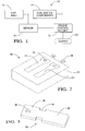
- FIG. 1 is a block diagram of a non-limiting system in accordance with present principles
- Figure 2 is a perspective view of a sensor made in accordance with present principles
- Figure 3 is a perspective view of a terminal with thermal relief structure
- Figure 4 is a detail perspective view showing a chamfered terminal hole
- Figure 5 is a flow chart of a first method of making the sensor using a photo resist layer
- Figure 6 is a flow chart of a second method of making the sensor using two molding steps with a carrier plastic.
- Figure 7 is a flow chart of a third method of making the sensor using laser etching.
- a system is shown, generally designated 10, which includes a vehicle fuel tank 12 that is cooperatively engaged with various fuel system components 14 such as injection systems, fuel pumps, etc.
- a sensor 16 in accordance with present principles is engaged with the fuel tank 12 and/or fuel system components 14 and can be immersed in fuel to sense, e.g., its percentage of ethanol concentration, level in the tank 12, etc.
- the sensor 16 can send signals to a computer such as an engine control module (ECM) 18 that in turn can use the signals to drive an output 20 such as a fuel tank level gage or fuel tank low level lamp or fuel pressure gage or other appropriate output device.
- ECM engine control module
- Figure 2 shows that the sensor 16 includes a polymer substrate 22 preferably made of acetal such as the acetal marketed under the trade name "Delrin.”
- the substrate 22 may be parallelepiped-shaped as shown.
- One or more electrical conductors may be disposed on the substrate 22.
- Each conductor 24, 26 is electrically connected to one or more respective metal terminals 28 that, in the embodiment shown in Figure 2 , are partially embedded in the substrate 22 and partially emerge from an end thereof. More particularly, an electrical path is established from a conductor 24/26 to a respective terminal 28 through a respective hole 30 that is formed in the substrate 22 in accordance with principles below.
- each terminal 28 is formed with a terminal opening 32 with which an electrical lead or connector can be engaged by, e.g., soldering, and each terminal 28 is also formed with thermal relief structure.
- the thermal relief structure is a narrower segment 34 that is formed between two wider segments 36, 38 of the otherwise parallelepiped-shaped terminal 28. The narrower segment 34 resists heat transfer from the solder in and around the terminal opening and the wider segment 36 to the opposed wider segment 38, which is embedded in the substrate 22.
- providing terminals with thermal relief structure permits soldering without unduly damaging the acetal substrate 22.
- FIG 4 shows that to facilitate smooth transition of plating between the conductors 24, 26 and respective terminals 28, the walls 40 of the holes 30 may be chamfered.
- the walls 40 slope inwardly as shown from the top surface of the substrate 22.
- Each hole 30 may have a square periphery as shown or a circular periphery or other suitably shaped periphery.
- a first method for making the sensor 16 is shown in Figure 5 . It is to be understood that in all embodiments the substrate 22 initially is made by overmolding the polymer onto the terminals 28.
- the holes 30 can be formed concurrently with the desired conductor patterns during etching or, more preferably, during the overmolding of the terminals.
- An extra inner shielding element made of thin metallic stock may also be incorporated into the substrate by overmolding.
- the shielding element terminates in or is soldered to a terminal. Or, if inner shielding is required it may be established by using two acetal substrates, plating a face of one substrate and then thermally bonding the two substrates together so that the shield is between the substrates.
- a photoresist layer is deposited on the substrate 22 by, e.g., gluing the resist layer to the substrate 22.
- the substrate with photoresist layer are exposed to light, e.g., ultraviolet light, in the desired pattern of the conductors to be subsequently plated.
- the photoresist layer is a mask that establishes the negative of the desired shape of the electrodes.
- the substrate with remaining photoresist is etched to form the desired patterns of the conductors 24, 26, which establish anchor points for the conductors to be plated.
- the etchant may be the substance marketed under the trade name "Delrin Etch.” The etch can be accomplished by submerging the substrate in a solution of the etchant. The mask is removed in accordance with photoresist removal principles known in the art.
- the conductors 24, 26 are deposited onto the patterns formed in the substrate 22, preferably using electroless plating techniques known in the art. If desired, the conductors 24, 26 may be protected by plating them with tin or aluminum through an electroplating process, and when aluminum is used it may be anodized.
- a second method for making the sensor 16 is shown in Figure 6 .
- a polymer such as acetal is molded into the substrate 22 with the desired pattern of the conductors 24, 26 formed in the mold.
- the substrate is overmolded with a carrier plastic, except for the parts of the substrate that form the desired pattern of the conductors. These portions are not overmolded.
- the carrier plastic is not sensitive to the etchant, so that only the portions of the substrate 22 that form the desired patterns of the conductors are etched at block 56.
- the conductors 24, 26 are then plated onto the substrate at block 58 in accordance with principles above. If desired, the carrier plastic may be removed.
- the initially molded part may be acrylonitrile-butadiene-styrene (ABS) and acetal may be used for the overmolding.
- ABS acrylonitrile-butadiene-styrene
- acetal may be used for the overmolding. The etching is done so that only the ABS, not the acetal, is etched. Then the ABS is plated.
- the acetal prior to molding at block 50 may be mixed with a metallization agent such as Palladium, and the carrier plastic used for overmolding at block 52 is non-metallized acetal, which promotes plating at block 56 after etching at block 54.
- a metallization agent such as Palladium
- Figure 7 shows that alternatively to etching using a solvent, the substrate 22 may be directly etched at block 5 8 using a laser to form the desired conductor patterns in the substrate. The etched substrate is then plated at block 60 in accordance with principles above.
Landscapes
- Physics & Mathematics (AREA)
- Thermal Sciences (AREA)
- Fluid Mechanics (AREA)
- General Physics & Mathematics (AREA)
- Electromagnetism (AREA)
- Engineering & Computer Science (AREA)
- Power Engineering (AREA)
- Investigating Or Analyzing Materials By The Use Of Electric Means (AREA)
Applications Claiming Priority (1)
| Application Number | Priority Date | Filing Date | Title |
|---|---|---|---|
| US11/973,179 US20090090179A1 (en) | 2007-10-05 | 2007-10-05 | Sensor with polymer substrate for use in corrosive liquids |
Publications (1)
| Publication Number | Publication Date |
|---|---|
| EP2045585A2 true EP2045585A2 (de) | 2009-04-08 |
Family
ID=39952170
Family Applications (1)
| Application Number | Title | Priority Date | Filing Date |
|---|---|---|---|
| EP08165530A Withdrawn EP2045585A2 (de) | 2007-10-05 | 2008-09-30 | Sensor mit einem Polymersubstrat für korrosive Flüssigkeiten |
Country Status (2)
| Country | Link |
|---|---|
| US (1) | US20090090179A1 (de) |
| EP (1) | EP2045585A2 (de) |
Families Citing this family (4)
| Publication number | Priority date | Publication date | Assignee | Title |
|---|---|---|---|---|
| WO2012090317A1 (ja) * | 2010-12-28 | 2012-07-05 | トヨタ自動車株式会社 | アルコール濃度センサの合理性診断装置 |
| US8973437B2 (en) * | 2012-09-25 | 2015-03-10 | Resource Conservation Technologies, Inc. | Condensate sensing device |
| US12422391B2 (en) | 2019-08-27 | 2025-09-23 | Chemelex Europe Gmbh | Ruggedized sensor for detecting organic liquids |
| USD953183S1 (en) | 2019-11-01 | 2022-05-31 | Nvent Services Gmbh | Fuel sensor |
-
2007
- 2007-10-05 US US11/973,179 patent/US20090090179A1/en not_active Abandoned
-
2008
- 2008-09-30 EP EP08165530A patent/EP2045585A2/de not_active Withdrawn
Also Published As
| Publication number | Publication date |
|---|---|
| US20090090179A1 (en) | 2009-04-09 |
Similar Documents
| Publication | Publication Date | Title |
|---|---|---|
| US12096549B1 (en) | Panel molded electronic assemblies with multi-surface conductive contacts | |
| US4985600A (en) | Printed circuit board having an injection molded substrate | |
| JPH08148240A (ja) | コネクタ | |
| KR19990014212A (ko) | 배선판 및 그 제조 방법과 무전해 도금 방법 | |
| EP2045585A2 (de) | Sensor mit einem Polymersubstrat für korrosive Flüssigkeiten | |
| EP0396248A2 (de) | Elektrischer Steckerstift und Verfahren zu seiner Herstellung | |
| US20120162860A1 (en) | Chip capacitor and method of manufacturing same | |
| WO2010001554A1 (ja) | 電子回路部品およびその製造方法 | |
| TW201322349A (zh) | 半導體封裝的製造方法、半導體封裝、以及半導體裝置 | |
| CN110678004B (zh) | 一种充电桩用pcb板的制作方法 | |
| KR20000022646A (ko) | 반도체 장치와 그 제조방법 및 이것에 사용하는 금속기판 | |
| US4236777A (en) | Integrated circuit package and manufacturing method | |
| CN1173614C (zh) | 用于在电绝缘的底座上形成金属的线路图的方法 | |
| KR102605794B1 (ko) | 배선 회로 기판, 및 촬상 장치 | |
| KR100756261B1 (ko) | 배선 기판의 제조 방법 | |
| US7670874B2 (en) | Plated pillar package formation | |
| US9622352B2 (en) | Manufacturing method for component incorporated substrate and component incorporated substrate | |
| US7951301B2 (en) | Method for producing a ceramic printed-circuit board | |
| CN221175883U (zh) | 贴片桥丝式点火电阻 | |
| US5766499A (en) | Method of making a circuitized substrate | |
| US20260025913A1 (en) | Circuit Board Structure, Manufacturing Method Thereof and Three-dimensional Electrical Connection Structure Including the Same | |
| CN222395029U (zh) | 一种lds天线组件及通信设备 | |
| KR100850221B1 (ko) | 감입식 피동부품의 제조방법 | |
| US7235432B2 (en) | Method for producing an electrical conductor element | |
| KR950000399B1 (ko) | 인쇄회로 기판 형성방법 |
Legal Events
| Date | Code | Title | Description |
|---|---|---|---|
| PUAI | Public reference made under article 153(3) epc to a published international application that has entered the european phase |
Free format text: ORIGINAL CODE: 0009012 |
|
| AK | Designated contracting states |
Kind code of ref document: A2 Designated state(s): AT BE BG CH CY CZ DE DK EE ES FI FR GB GR HR HU IE IS IT LI LT LU LV MC MT NL NO PL PT RO SE SI SK TR |
|
| AX | Request for extension of the european patent |
Extension state: AL BA MK RS |
|
| STAA | Information on the status of an ep patent application or granted ep patent |
Free format text: STATUS: THE APPLICATION IS DEEMED TO BE WITHDRAWN |
|
| 18D | Application deemed to be withdrawn |
Effective date: 20110401 |