EP2045371A2 - Method and apparatus for manufacturing an ultra low defect semiconductor single crystalline ingot - Google Patents
Method and apparatus for manufacturing an ultra low defect semiconductor single crystalline ingot Download PDFInfo
- Publication number
- EP2045371A2 EP2045371A2 EP08017323A EP08017323A EP2045371A2 EP 2045371 A2 EP2045371 A2 EP 2045371A2 EP 08017323 A EP08017323 A EP 08017323A EP 08017323 A EP08017323 A EP 08017323A EP 2045371 A2 EP2045371 A2 EP 2045371A2
- Authority
- EP
- European Patent Office
- Prior art keywords
- single crystalline
- crystalline ingot
- melt
- semiconductor
- manufacturing
- Prior art date
- Legal status (The legal status is an assumption and is not a legal conclusion. Google has not performed a legal analysis and makes no representation as to the accuracy of the status listed.)
- Granted
Links
- 239000004065 semiconductor Substances 0.000 title claims abstract description 37
- 238000000034 method Methods 0.000 title claims abstract description 36
- 230000007547 defect Effects 0.000 title claims abstract description 35
- 238000004519 manufacturing process Methods 0.000 title claims abstract description 30
- 239000010453 quartz Substances 0.000 claims abstract description 16
- VYPSYNLAJGMNEJ-UHFFFAOYSA-N silicon dioxide Inorganic materials O=[Si]=O VYPSYNLAJGMNEJ-UHFFFAOYSA-N 0.000 claims abstract description 16
- 230000003247 decreasing effect Effects 0.000 claims abstract description 10
- 239000007788 liquid Substances 0.000 claims abstract description 9
- 238000007598 dipping method Methods 0.000 claims abstract description 6
- 238000002231 Czochralski process Methods 0.000 claims abstract description 5
- 239000000155 melt Substances 0.000 claims description 33
- XUIMIQQOPSSXEZ-UHFFFAOYSA-N Silicon Chemical compound [Si] XUIMIQQOPSSXEZ-UHFFFAOYSA-N 0.000 description 31
- 229910052710 silicon Inorganic materials 0.000 description 31
- 239000010703 silicon Substances 0.000 description 31
- 238000009826 distribution Methods 0.000 description 9
- 238000010586 diagram Methods 0.000 description 4
- 230000005672 electromagnetic field Effects 0.000 description 4
- 238000010438 heat treatment Methods 0.000 description 4
- 238000007711 solidification Methods 0.000 description 4
- 230000008023 solidification Effects 0.000 description 4
- 230000005540 biological transmission Effects 0.000 description 3
- 230000007423 decrease Effects 0.000 description 3
- 238000013461 design Methods 0.000 description 3
- 239000011261 inert gas Substances 0.000 description 3
- 238000012986 modification Methods 0.000 description 3
- 230000004048 modification Effects 0.000 description 3
- XKRFYHLGVUSROY-UHFFFAOYSA-N Argon Chemical compound [Ar] XKRFYHLGVUSROY-UHFFFAOYSA-N 0.000 description 2
- 239000013078 crystal Substances 0.000 description 2
- 229910052786 argon Inorganic materials 0.000 description 1
- 238000007796 conventional method Methods 0.000 description 1
- 238000001816 cooling Methods 0.000 description 1
- 238000002425 crystallisation Methods 0.000 description 1
- 230000008025 crystallization Effects 0.000 description 1
- 238000009792 diffusion process Methods 0.000 description 1
- 230000000694 effects Effects 0.000 description 1
- 239000007789 gas Substances 0.000 description 1
- 230000020169 heat generation Effects 0.000 description 1
- 238000009434 installation Methods 0.000 description 1
- 238000005259 measurement Methods 0.000 description 1
- 230000003647 oxidation Effects 0.000 description 1
- 238000007254 oxidation reaction Methods 0.000 description 1
- 230000002093 peripheral effect Effects 0.000 description 1
- 229910021420 polycrystalline silicon Inorganic materials 0.000 description 1
- 230000005855 radiation Effects 0.000 description 1
- 239000000758 substrate Substances 0.000 description 1
Images


Classifications
-
- C—CHEMISTRY; METALLURGY
- C30—CRYSTAL GROWTH
- C30B—SINGLE-CRYSTAL GROWTH; UNIDIRECTIONAL SOLIDIFICATION OF EUTECTIC MATERIAL OR UNIDIRECTIONAL DEMIXING OF EUTECTOID MATERIAL; REFINING BY ZONE-MELTING OF MATERIAL; PRODUCTION OF A HOMOGENEOUS POLYCRYSTALLINE MATERIAL WITH DEFINED STRUCTURE; SINGLE CRYSTALS OR HOMOGENEOUS POLYCRYSTALLINE MATERIAL WITH DEFINED STRUCTURE; AFTER-TREATMENT OF SINGLE CRYSTALS OR A HOMOGENEOUS POLYCRYSTALLINE MATERIAL WITH DEFINED STRUCTURE; APPARATUS THEREFOR
- C30B15/00—Single-crystal growth by pulling from a melt, e.g. Czochralski method
- C30B15/20—Controlling or regulating
-
- C—CHEMISTRY; METALLURGY
- C30—CRYSTAL GROWTH
- C30B—SINGLE-CRYSTAL GROWTH; UNIDIRECTIONAL SOLIDIFICATION OF EUTECTIC MATERIAL OR UNIDIRECTIONAL DEMIXING OF EUTECTOID MATERIAL; REFINING BY ZONE-MELTING OF MATERIAL; PRODUCTION OF A HOMOGENEOUS POLYCRYSTALLINE MATERIAL WITH DEFINED STRUCTURE; SINGLE CRYSTALS OR HOMOGENEOUS POLYCRYSTALLINE MATERIAL WITH DEFINED STRUCTURE; AFTER-TREATMENT OF SINGLE CRYSTALS OR A HOMOGENEOUS POLYCRYSTALLINE MATERIAL WITH DEFINED STRUCTURE; APPARATUS THEREFOR
- C30B15/00—Single-crystal growth by pulling from a melt, e.g. Czochralski method
- C30B15/14—Heating of the melt or the crystallised materials
-
- C—CHEMISTRY; METALLURGY
- C30—CRYSTAL GROWTH
- C30B—SINGLE-CRYSTAL GROWTH; UNIDIRECTIONAL SOLIDIFICATION OF EUTECTIC MATERIAL OR UNIDIRECTIONAL DEMIXING OF EUTECTOID MATERIAL; REFINING BY ZONE-MELTING OF MATERIAL; PRODUCTION OF A HOMOGENEOUS POLYCRYSTALLINE MATERIAL WITH DEFINED STRUCTURE; SINGLE CRYSTALS OR HOMOGENEOUS POLYCRYSTALLINE MATERIAL WITH DEFINED STRUCTURE; AFTER-TREATMENT OF SINGLE CRYSTALS OR A HOMOGENEOUS POLYCRYSTALLINE MATERIAL WITH DEFINED STRUCTURE; APPARATUS THEREFOR
- C30B15/00—Single-crystal growth by pulling from a melt, e.g. Czochralski method
- C30B15/20—Controlling or regulating
- C30B15/203—Controlling or regulating the relationship of pull rate (v) to axial thermal gradient (G)
-
- C—CHEMISTRY; METALLURGY
- C30—CRYSTAL GROWTH
- C30B—SINGLE-CRYSTAL GROWTH; UNIDIRECTIONAL SOLIDIFICATION OF EUTECTIC MATERIAL OR UNIDIRECTIONAL DEMIXING OF EUTECTOID MATERIAL; REFINING BY ZONE-MELTING OF MATERIAL; PRODUCTION OF A HOMOGENEOUS POLYCRYSTALLINE MATERIAL WITH DEFINED STRUCTURE; SINGLE CRYSTALS OR HOMOGENEOUS POLYCRYSTALLINE MATERIAL WITH DEFINED STRUCTURE; AFTER-TREATMENT OF SINGLE CRYSTALS OR A HOMOGENEOUS POLYCRYSTALLINE MATERIAL WITH DEFINED STRUCTURE; APPARATUS THEREFOR
- C30B15/00—Single-crystal growth by pulling from a melt, e.g. Czochralski method
- C30B15/20—Controlling or regulating
- C30B15/206—Controlling or regulating the thermal history of growing the ingot
-
- C—CHEMISTRY; METALLURGY
- C30—CRYSTAL GROWTH
- C30B—SINGLE-CRYSTAL GROWTH; UNIDIRECTIONAL SOLIDIFICATION OF EUTECTIC MATERIAL OR UNIDIRECTIONAL DEMIXING OF EUTECTOID MATERIAL; REFINING BY ZONE-MELTING OF MATERIAL; PRODUCTION OF A HOMOGENEOUS POLYCRYSTALLINE MATERIAL WITH DEFINED STRUCTURE; SINGLE CRYSTALS OR HOMOGENEOUS POLYCRYSTALLINE MATERIAL WITH DEFINED STRUCTURE; AFTER-TREATMENT OF SINGLE CRYSTALS OR A HOMOGENEOUS POLYCRYSTALLINE MATERIAL WITH DEFINED STRUCTURE; APPARATUS THEREFOR
- C30B29/00—Single crystals or homogeneous polycrystalline material with defined structure characterised by the material or by their shape
- C30B29/02—Elements
- C30B29/06—Silicon
-
- H—ELECTRICITY
- H01—ELECTRIC ELEMENTS
- H01L—SEMICONDUCTOR DEVICES NOT COVERED BY CLASS H10
- H01L21/00—Processes or apparatus adapted for the manufacture or treatment of semiconductor or solid state devices or of parts thereof
- H01L21/02—Manufacture or treatment of semiconductor devices or of parts thereof
- H01L21/04—Manufacture or treatment of semiconductor devices or of parts thereof the devices having at least one potential-jump barrier or surface barrier, e.g. PN junction, depletion layer or carrier concentration layer
- H01L21/18—Manufacture or treatment of semiconductor devices or of parts thereof the devices having at least one potential-jump barrier or surface barrier, e.g. PN junction, depletion layer or carrier concentration layer the devices having semiconductor bodies comprising elements of Group IV of the Periodic System or AIIIBV compounds with or without impurities, e.g. doping materials
- H01L21/20—Deposition of semiconductor materials on a substrate, e.g. epitaxial growth solid phase epitaxy
-
- Y—GENERAL TAGGING OF NEW TECHNOLOGICAL DEVELOPMENTS; GENERAL TAGGING OF CROSS-SECTIONAL TECHNOLOGIES SPANNING OVER SEVERAL SECTIONS OF THE IPC; TECHNICAL SUBJECTS COVERED BY FORMER USPC CROSS-REFERENCE ART COLLECTIONS [XRACs] AND DIGESTS
- Y10—TECHNICAL SUBJECTS COVERED BY FORMER USPC
- Y10T—TECHNICAL SUBJECTS COVERED BY FORMER US CLASSIFICATION
- Y10T117/00—Single-crystal, oriented-crystal, and epitaxy growth processes; non-coating apparatus therefor
- Y10T117/10—Apparatus
- Y10T117/1024—Apparatus for crystallization from liquid or supercritical state
- Y10T117/1032—Seed pulling
- Y10T117/1068—Seed pulling including heating or cooling details [e.g., shield configuration]
Definitions
- a process margin in the manufacture of a defect-free single crystalline ingot is influenced by a vertical temperature gradient of a radial direction, and thus invariably, the temperature gradient should be large and uniform in a radial direction.
- a conventional technique for manufacturing a single crystalline ingot of 12 inch diameter and at least 300kg or 400kg weight exhibits a narrow process margin due to reduction in a G value of an edge portion, and when manufacturing an Si wafer, causes a DSOD (Direct Surface Oxide Defect) defect (See FIG. 2(b) ) in the shape of a ring at a peripheral portion of the wafer, thereby failing to manufacture a defect-free wafer, in which a defect-free margin is uniformly maintained in a radial direction.
- DSOD Direct Surface Oxide Defect
- a charge size is small, for example a single crystalline ingot is grown to 400kg or 300kg or less, a latent heat of solidification is relatively small, and thus a pulling speed should be controlled uniformly from an initial stage of growth to the last stage to maintain a margin uniformly, which may reduce productivity.
- FIG. 3 shows that as a G value of an edge portion of a single crystalline ingot reduces at the last stage of a single crystalline ingot growth process, a defect-free margin at the last stage remarkably reduces in comparison with a defect-free margin at an initial stage.
- this is mainly resulted from a change of latent heat due to change in a residual melt, and reduction in a G value of an edge portion caused by change in the shape of a melt flow and heat transmission due to a hot zone.
- the present invention is designed to solve the problems of the prior arts. Therefore, it is an object of the present invention to provide a method and apparatus for manufacturing an ultra low defect semiconductor single crystalline ingot that controls a cooling efficiency of a single crystalline ingot according to length of the single crystalline ingot to uniformly maintain or increase a defect-free margin throughout a process and improve a pulling speed.
- the present invention provides a method for manufacturing an ultra low defect semiconductor single crystalline ingot that uses a Czochralski process for growing a semiconductor single crystalline ingot through a solid-liquid interface by dipping a seed into a semiconductor melt received in a quartz crucible and slowly pulling up the seed while rotating the seed, wherein a defect-free margin is controlled by increasing or decreasing a heat space on a surface of the semiconductor melt according to change in length of the single crystalline ingot as progress of the single crystalline ingot growth process.
- the heat space may be increased or decreased by differentially changing a melt gap between a bottom of a heat shield structure spaced away from an outer periphery of the single crystalline ingot and the surface of the semiconductor melt according to length of the single crystalline ingot.
- the melt gap is controlled in the range of 25mm or less.
- an apparatus for manufacturing an ultra low defect semiconductor single crystalline ingot that performs a Czochralski process for growing a semiconductor single crystalline ingot through a solid-liquid interface by dipping a seed into a semiconductor melt received in a quartz crucible and slowly pulling up the seed while rotating the seed, includes a heat space control unit for controlling a defect-free margin by increasing or decreasing a heat space on a surface of the semiconductor melt according to change in length of the single crystalline ingot as progress of the single crystalline ingot growth process.
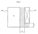
- FIG. 4 is a side view showing schematically a heat space on a silicon melt for description of a method for manufacturing an ultra low defect single crystalline ingot according to a preferred embodiment of the present invention.
- the present invention performs a Czochralksi process for growing a silicon single crystalline ingot 100 through a solid-liquid interface by dipping a seed into a silicon melt received in a quartz crucible and pulling up the seed while rotating the seed, and during crystalline ingot growth, controls a heat space (slanted lines) on a surface of a silicon melt or efficiency of the heat space to control a defect-free margin.
- the heat space is increased or decreased by changing a location of the heat shield structure 101 according to change in length of the silicon single crystalline ingot 100 as progress of a single crystalline ingot growth process.
- the heat space may be controlled by changing a gap, or a melt gap (A) between the surface of the silicon melt and the bottom of the heat shield structure 101, or an interval (B) between the outer periphery of the silicon single crystalline ingot 100 and the heat shield structure 101, or a combination thereof.
- the present invention changes a melt gap according to length of a single crystalline ingot during a single crystalline ingot growth process, so a temperature gradient in a radial direction is uniformly maintained from an initial stage of crystalline ingot growth (See FIG. 5(a) ) to an intermediate stage of crystalline ingot growth and thereafter (See FIG. 5(b) ).
- a defect-free margin can be maintained uniformly, and both of G values of a center portion and an edge portion are increased to improve a pulling speed.
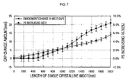
- FIG. 7 shows an actual experimental example, in which the heat space is reduced by decreasing a melt gap according to change in length of a growing single crystalline ingot for smooth heat radiation.
- a horizontal axis is a length of a single crystalline ingot changing according to crystalline ingot growth
- a left vertical axis is a change (reduction) amount of a melt gap
- a right vertical axis is an increasing rate of pulling speed (PS).
- PS pulling speed
- the PS increasing rate indicates the percentage of a degree of an improved PS value to a previous PS value.
- a pulling speed (V) of the single crystalline ingot is set to satisfy the following equation.
- V a + b * L + C * (a, b, c: constant, L: length of a single crystalline ingot, ⁇ Gap: a change amount of a melt gap)
- FIG. 8 is a graph showing an example of a change in a defect-free margin according to level of reduction of a heat space through reduction of a melt gap. It is found that as a melt gap is reduced to 12 to 14mm, a defect-free margin that was 0.01mm /min at an initial point, is increased up to 0.025mm/min or more, and thereafter is reduced. This shows that as reduction in a G value of an edge portion of a single crystalline ingot is improved according to level of a melt gap, a quality margin is improved, but in the case that the G value exceeds a critical value, the excessively increased G value of the edge portion causes a relative reduction of a G value of a center portion of the single crystalline ingot, which is opposite to the conventional phenomenon.
- a control pattern of the heat space can be variably changed depending on structure or shape of a heat shield structure. That is, for example, in the case that a space surround by the heat shield structure is relatively narrow, the heat space can be controlled by setting a level of change in a melt gap relatively small.
- a level of reduction of the melt gap is set to 25mm or less as shown in FIG. 7 .
- FIG. 9 is a view showing a main configuration of an apparatus for manufacturing a single crystalline ingot according to a preferred embodiment of the present invention.
- the quartz crucible rotating means 30 is installed below the crucible support 20, and rotates the crucible support 20 and the quartz crucible 10 and slowly moves up the quartz crucible 10 in order to uniformly maintain the height of a solid-liquid interface.
- the heating means 40 is spaced a predetermined distance away from a side wall of the crucible support 20 and heats the quartz crucible 10.
- the adiabatic means 50 is installed outside of the heating means 40 and prevents heat generated from the heating means 40 from emitting to the external environment.
- the single crystalline ingot pulling means 60 pulls a silicon single crystalline ingot 100 from the silicon melt (SM) received in the quartz crucible 10 by use of a seed rotating in a predetermined direction.
- the heat shield structure 101 is spaced a predetermined distance away from an outer periphery of the silicon single crystalline ingot 100 and shields heat emitted from the silicon single crystalline ingot 100.
- the inert gas supply means (not shown) supplies an inert gas (for example, Ar gas) to an upper surface of the silicon melt (SM) along the outer periphery of the silicon single crystalline ingot 100.
- the heat space control unit 200 controls a heat space on the silicon melt (SM).
- the heat space control unit 200 controls the heat space, for examples, increases or decreases the heat space according to change in length of the single crystalline ingot as progress of a single crystalline ingot growth process.
- the heat space may be controlled by changing a location of the heat shield structure, however the present invention is not limited in this regard.
- the heat space control unit 200 includes a predetermined drive tool and a controller for controlling the drive tool to increase or decrease the heat space by moving the heat shield structure 101.
- the present invention controls the heat space on the silicon melt to uniformly maintain a temperature gradient in a radial direction ranging from a center portion to an edge portion of the single crystalline ingot, thereby substantially sufficiently securing a defect-free margin from an initial stage of crystalline ingot growth to a last stage of crystalline ingot growth.
- the entire G value according to length of the single crystal increases to improve a pulling speed and consequently increase productivity, and to eliminate the need for change in design of the heat shield structure, thereby reducing the installation costs.
- the present invention can be advantageously applicable to, in particular, 12 inch defect-free silicon single crystalline ingot growth. That is, in the case of a 12 inch silicon single crystal manufactured with a large quantity charge of at least 300kg or 400kg, a crucible receiving a silicon melt and a heat shield structure surrounding the crucible are increased in size, and consequently an amount of heat accumulated in the heat shield structure is remarkably increased. Further, the convection of the silicon melt is suppressed by a strong electromagnetic field of at least 2000G or 3000G applied during the process, thereby suppressing heat emission, so that a G value of the edge portion of the single crystalline ingot is lowered.
- the present invention can solve the above-mentioned problems by decreasing the heat space.
Abstract
Description
- The present invention relates to a method and apparatus for manufacturing an ultra low defect semiconductor single crystalline ingot, and in particular, to a method and apparatus for manufacturing an ultra low defect semiconductor single crystalline ingot, in which a temperature gradient is uniform in a radial direction of a single crystalline ingot and a defect-free margin is maintained in a lengthwise direction of a single crystalline ingot.
- As a semiconductor device process moves toward a finer level, for example a nanometer level, even a crystalline defect having size of several tens of nanometers causes reduction in yield of devices. Accordingly, semiconductor device makers increasingly use a wafer having the controlled crystalline defects as a semiconductor substrate.
- However, based on Voronkov's theory, a process margin in the manufacture of a defect-free single crystalline ingot is influenced by a vertical temperature gradient of a radial direction, and thus invariably, the temperature gradient should be large and uniform in a radial direction.
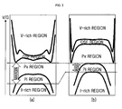
- According to Voronkov's theory, as shown in
FIG. 1 , in the case that a V/G value is larger than a critical value due to high speed growth, a vacancy-rich (V-rich) region is formed, which may be resulted from voids. In the case that a V/G value is smaller than a critical value due to low speed growth, an OSF (Oxidation induced Stacking Fault) region is formed near a crystalline. In the case of lower speed growth, an interstitial-rich (I-rich) region is formed that is resulted from a dislocation loop formed by concentration of interstitial silicon. And, a defect-free region that is neither a V-rich region nor an I-rich region is formed between the V-rich region and the I-rich region. The defect-free region includes a Pv region, or a residual vacancy type defect-free region and a Pi region, or a residual interstitial type defect-free region. In V/G, V indicates a pulling speed of a single crystalline ingot and is a convection term of a point defect in the silicon single crystalline. And, G indicates an axial temperature gradient near an interface of a melt and is a diffusion term of a point defect by the temperature gradient in a crystalline. - Generally, in the manufacture of a single crystalline wafer, a margin of a defect-free region is influenced by a temperature gradient of a radial direction, and thus a difference (ΔG) in G value between a center portion of the single crystalline ingot and an edge portion should be small in order to create a uniform temperature gradient in a radial direction.
- Conventionally, to manufacture a single crystalline wafer of high margin of a defect-free region, attempts have been made to design a hot zone (HZ) of a heat shield structure located on a solid-liquid interface in various shapes to control a G value of a single crystalline ingot or to adjust a relative location from a maximum heat generation portion of a heater to a surface of a melt to control the convection of a melt or a heat transmission path. And, studies have been made to improve a parameter such as an argon (Ar) flow ratio, a ratio between seed rotation (SR) speed and crucible rotation (CR) speed or types of an electromagnetic field. The related techniques are disclosed in, for example
JP Laid-open Patent Publication Nos. 2005-015296 2006-069803 2004-137093 - However, modification to design of a hot zone needs an additional device, and inevitably results in an increase of volume of an equipment, and in the case that a G value of any one of a center portion and an edge portion of a single crystalline ingot is improved, a G value of the other portion is deteriorated. For example, if a bottom of a heat shield structure is designed to be large or thick, the increased degree of a G value of a center portion is trivial in comparison with the increased degree of a G value of an edge portion. As a result, ΔG value is deteriorated.
- On the other hand, in the case that an electromagnetic field is improved, change of the electromagnetic field causes change in type of convection of a melt and consequently may reduce a G value or deteriorate ΔG value. And, it is found that a method for optimizing a parameter such as Ar, pressure or SR/CR ratio has a trivial effect.
- As shown in
FIG. 2(a) , a conventional technique for manufacturing a single crystalline ingot of 12 inch diameter and at least 300kg or 400kg weight exhibits a narrow process margin due to reduction in a G value of an edge portion, and when manufacturing an Si wafer, causes a DSOD (Direct Surface Oxide Defect) defect (SeeFIG. 2(b) ) in the shape of a ring at a peripheral portion of the wafer, thereby failing to manufacture a defect-free wafer, in which a defect-free margin is uniformly maintained in a radial direction. - And, as disclosed in
JP Laid-open Patent Publication No. 2005-015296 - As an example of the prior art,
FIG. 3 shows that as a G value of an edge portion of a single crystalline ingot reduces at the last stage of a single crystalline ingot growth process, a defect-free margin at the last stage remarkably reduces in comparison with a defect-free margin at an initial stage. As mentioned above, this is mainly resulted from a change of latent heat due to change in a residual melt, and reduction in a G value of an edge portion caused by change in the shape of a melt flow and heat transmission due to a hot zone. - The present invention is designed to solve the problems of the prior arts. Therefore, it is an object of the present invention to provide a method and apparatus for manufacturing an ultra low defect semiconductor single crystalline ingot that controls a cooling efficiency of a single crystalline ingot according to length of the single crystalline ingot to uniformly maintain or increase a defect-free margin throughout a process and improve a pulling speed.
- In order to achieve the object of the present invention, the present invention provides a method for manufacturing an ultra low defect semiconductor single crystalline ingot that uses a Czochralski process for growing a semiconductor single crystalline ingot through a solid-liquid interface by dipping a seed into a semiconductor melt received in a quartz crucible and slowly pulling up the seed while rotating the seed, wherein a defect-free margin is controlled by increasing or decreasing a heat space on a surface of the semiconductor melt according to change in length of the single crystalline ingot as progress of the single crystalline ingot growth process.
- Preferably, the heat space may be increased or decreased by differentially changing a melt gap between a bottom of a heat shield structure spaced away from an outer periphery of the single crystalline ingot and the surface of the semiconductor melt according to length of the single crystalline ingot.
- Preferably, the melt gap is controlled in the range of 25mm or less.
- Preferably, a pulling speed (V) of the single crystalline ingot is changed to satisfy an equation:

- The heat space may be increased or decreased by differentially changing an interval between a heat shield structure spaced away from an outer periphery of the single crystalline ingot and the outer periphery of the single crystalline ingot according to length of the single crystalline ingot.
- According to another aspect of the present invention, an apparatus for manufacturing an ultra low defect semiconductor single crystalline ingot that performs a Czochralski process for growing a semiconductor single crystalline ingot through a solid-liquid interface by dipping a seed into a semiconductor melt received in a quartz crucible and slowly pulling up the seed while rotating the seed, includes a heat space control unit for controlling a defect-free margin by increasing or decreasing a heat space on a surface of the semiconductor melt according to change in length of the single crystalline ingot as progress of the single crystalline ingot growth process.
- The present invention will be more fully described in the following detailed description, taken accompanying drawings, however, the description proposed herein is just a preferable example for the purpose of illustrations, not intended to limit the scope of the invention.
-
FIG. 1 is a defect distribution diagram showing a vertical defect distribution when growing a silicon single crystalline ingot of 12 inch diameter and 400kg weight. -
FIG. 2(a) is a temperature distribution diagram showing an actual defect distribution of the silicon single crystalline ingot ofFIG. 1 , andFIG. 2(b) is a photograph of a cross section showing an actual defect distribution of the silicon single crystalline ingot ofFIG. 1 . -
FIG. 3 is a defect distribution diagram showing a change in a defect-free margin by a conventional single crystalline ingot growth process. -
FIG. 4 is a side view showing schematically a heat space on a silicon melt for description of a method for manufacturing an ultra low defect single crystalline ingot according to a preferred embodiment of the present invention. -
FIG. 5 is a defect distribution diagram showing a defect-free margin maintained uniformly by a method for manufacturing an ultra low defect single crystalline ingot according to a preferred embodiment of the present invention. -
FIG. 6 is a photograph of a cross section showing analysis using a Cu-haze method of an actual defect distribution of a single crystalline ingot manufactured according to a preferred embodiment of the present invention. -
FIG. 7 is a graph showing a change amount of melt gap and an increasing rate of pulling speed according to length of a single crystalline ingot, controlled according to a preferred embodiment of the present invention. -
FIG. 8 is a graph showing a change in a defect-free margin according to change in a melt gap. -
FIG. 9 is a view showing a main configuration of an apparatus for manufacturing a single crystalline ingot according to a preferred embodiment of the present invention. - Hereinafter, preferred embodiments of the present invention will be described in detail with reference to the accompanying drawings. Prior to the description, it should be understood that the terms used in the specification and the appended claims should not be construed as limited to general and dictionary meanings, but interpreted based on the meanings and concepts corresponding to technical aspects of the present invention on the basis of the principle that the inventor is allowed to define terms appropriately for the best explanation. Therefore, the description proposed herein is just a preferable example for the purpose of illustrations only, not intended to limit the scope of the invention, so it should be understood that other equivalents and modifications could be made thereto without departing from the spirit and scope of the invention.
-
FIG. 4 is a side view showing schematically a heat space on a silicon melt for description of a method for manufacturing an ultra low defect single crystalline ingot according to a preferred embodiment of the present invention. - The present invention performs a Czochralksi process for growing a silicon single
crystalline ingot 100 through a solid-liquid interface by dipping a seed into a silicon melt received in a quartz crucible and pulling up the seed while rotating the seed, and during crystalline ingot growth, controls a heat space (slanted lines) on a surface of a silicon melt or efficiency of the heat space to control a defect-free margin. - The heat space includes a space between an outer periphery of the silicon single
crystalline ingot 100 and aheat shield structure 101 and a space between the surface of the silicon melt and a bottom of theheat shield structure 101, and is a space where heat emitted from the silicon singlecrystalline ingot 100 is accumulated. - Preferably, the heat space is increased or decreased by changing a location of the
heat shield structure 101 according to change in length of the silicon singlecrystalline ingot 100 as progress of a single crystalline ingot growth process. For example, the heat space may be controlled by changing a gap, or a melt gap (A) between the surface of the silicon melt and the bottom of theheat shield structure 101, or an interval (B) between the outer periphery of the silicon singlecrystalline ingot 100 and theheat shield structure 101, or a combination thereof. - The present invention changes a melt gap according to length of a single crystalline ingot during a single crystalline ingot growth process, so a temperature gradient in a radial direction is uniformly maintained from an initial stage of crystalline ingot growth (See
FIG. 5(a) ) to an intermediate stage of crystalline ingot growth and thereafter (SeeFIG. 5(b) ). As a result, a defect-free margin can be maintained uniformly, and both of G values of a center portion and an edge portion are increased to improve a pulling speed. -
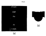
FIG. 6 shows analysis results that a vertical defect distribution of a single crystalline ingot grown according to the present invention is analyzed using a Cu-haze method. Referring toFIG. 6 , it is found that a defect-free margin is maintained by a change in a melt gap according to length of the single crystalline ingot, in particular, subsequent to the intermediate stage of crystalline ingot growth, although the pulling speed is changed up to 0.02mm/min or more, a defect-free margin of the initial stage of crystalline ingot growth is maintained, so that small-size vacancy defects occurred to the edge portion of the single crystalline ingot earlier are improved, and as shown in DSOD (Direct Surface Oxide Defect) measurement results (SeeFIG. 6(b) ), a defect-free region is distributed over the entire surface of a wafer. -
FIG. 7 shows an actual experimental example, in which the heat space is reduced by decreasing a melt gap according to change in length of a growing single crystalline ingot for smooth heat radiation. In the graph, a horizontal axis is a length of a single crystalline ingot changing according to crystalline ingot growth, a left vertical axis is a change (reduction) amount of a melt gap, and a right vertical axis is an increasing rate of pulling speed (PS). Here, the PS increasing rate indicates the percentage of a degree of an improved PS value to a previous PS value. - Referring to
FIG. 7 , it is found that reduction of the melt gap starts from the initial stage of crystalline ingot growth, and an increasing rate of a pulling speed starts to increase remarkably subsequent to the intermediate stage and further increases toward the last stage. Here, preferably a pulling speed (V) of the single crystalline ingot is set to satisfy the following equation.
-
FIG. 8 is a graph showing an example of a change in a defect-free margin according to level of reduction of a heat space through reduction of a melt gap. It is found that as a melt gap is reduced to 12 to 14mm, a defect-free margin that was 0.01mm /min at an initial point, is increased up to 0.025mm/min or more, and thereafter is reduced. This shows that as reduction in a G value of an edge portion of a single crystalline ingot is improved according to level of a melt gap, a quality margin is improved, but in the case that the G value exceeds a critical value, the excessively increased G value of the edge portion causes a relative reduction of a G value of a center portion of the single crystalline ingot, which is opposite to the conventional phenomenon. Thus, preferably the melt gap is reduced to 12 to 14mm in the example shown inFIG. 8 . As mentioned above, the present invention appropriate controls a heat space to uniformly control a temperature gradient in a radial direction of a single crystalline ingot, so that a sufficient defect-free margin can be secured and a pulling speed can be improved through increase of the entire G value of the single crystalline ingot. - In the present invention, a control pattern of the heat space can be variably changed depending on structure or shape of a heat shield structure. That is, for example, in the case that a space surround by the heat shield structure is relatively narrow, the heat space can be controlled by setting a level of change in a melt gap relatively small. In consideration of structure, shape or size of a general heat shield structure, preferably a level of reduction of the melt gap is set to 25mm or less as shown in
FIG. 7 . - And, the heat space can be controlled by slowly increasing a melt gap according to G values of a center portion and an edge portion of a single crystalline ingot and ΔG level.
-
FIG. 9 is a view showing a main configuration of an apparatus for manufacturing a single crystalline ingot according to a preferred embodiment of the present invention. - Referring to
FIG. 9 , the manufacturing apparatus includes aquartz crucible 10, acrucible support 20, a quartzcrucible rotating means 30, a heating means 40, an adiabatic means 50, a single crystallineingot pulling means 60, aheat shield structure 101, an inert gas supply means (not shown), and a heatspace control unit 200. Thequartz crucible 10 receives a silicon melt (SM) that a multicrystalline silicon is melt with high temperature. Thecrucible support 20 surrounds an outer periphery of thequartz crucible 10, and supports thequartz crucible 10 in a uniform shape at a high temperature atmosphere. The quartzcrucible rotating means 30 is installed below thecrucible support 20, and rotates thecrucible support 20 and thequartz crucible 10 and slowly moves up thequartz crucible 10 in order to uniformly maintain the height of a solid-liquid interface. The heating means 40 is spaced a predetermined distance away from a side wall of thecrucible support 20 and heats thequartz crucible 10. The adiabatic means 50 is installed outside of the heating means 40 and prevents heat generated from the heating means 40 from emitting to the external environment. The single crystallineingot pulling means 60 pulls a silicon singlecrystalline ingot 100 from the silicon melt (SM) received in thequartz crucible 10 by use of a seed rotating in a predetermined direction. Theheat shield structure 101 is spaced a predetermined distance away from an outer periphery of the silicon singlecrystalline ingot 100 and shields heat emitted from the silicon singlecrystalline ingot 100. The inert gas supply means (not shown) supplies an inert gas (for example, Ar gas) to an upper surface of the silicon melt (SM) along the outer periphery of the silicon singlecrystalline ingot 100. The heatspace control unit 200 controls a heat space on the silicon melt (SM). - The heat
space control unit 200 controls the heat space, for examples, increases or decreases the heat space according to change in length of the single crystalline ingot as progress of a single crystalline ingot growth process. The heat space may be controlled by changing a location of the heat shield structure, however the present invention is not limited in this regard. Although not shown inFIG. 9 , the heatspace control unit 200 includes a predetermined drive tool and a controller for controlling the drive tool to increase or decrease the heat space by moving theheat shield structure 101. - In the case that the heat space is controlled by changing a location of the
heat shield 101, the heatspace control unit 200 may perform a drive control to change a melt gap between the surface of the silicon melt (SM) and theheat shield structure 101, or an interval between the outer periphery of the silicon single crystalline ingot and the heat shield structure, or a combination thereof. - Preferably, the heat
space control unit 200 decreases the melt gap by moving down theheat shield structure 101 according to change in length of the single crystalline ingot as progress of the single crystalline ingot growth process. At this time, as shown inFIG. 7 , the melt gap is preferably controlled in the range of 25mm or less in consideration of an increasing rate of pulling speed or a defect-free margin. - The apparatus for manufacturing a single crystalline ingot according to the present invention has the same configuration as a typical apparatus for manufacturing a single crystalline ingot using a Czochralisk method known in the art, except the heat
space control unit 200, and the detailed description of the same configuration is omitted. - The present invention controls the heat space on the silicon melt to uniformly maintain a temperature gradient in a radial direction ranging from a center portion to an edge portion of the single crystalline ingot, thereby substantially sufficiently securing a defect-free margin from an initial stage of crystalline ingot growth to a last stage of crystalline ingot growth.
- According to the present invention, the entire G value according to length of the single crystal increases to improve a pulling speed and consequently increase productivity, and to eliminate the need for change in design of the heat shield structure, thereby reducing the installation costs.
- The present invention can be advantageously applicable to, in particular, 12 inch defect-free silicon single crystalline ingot growth. That is, in the case of a 12 inch silicon single crystal manufactured with a large quantity charge of at least 300kg or 400kg, a crucible receiving a silicon melt and a heat shield structure surrounding the crucible are increased in size, and consequently an amount of heat accumulated in the heat shield structure is remarkably increased. Further, the convection of the silicon melt is suppressed by a strong electromagnetic field of at least 2000G or 3000G applied during the process, thereby suppressing heat emission, so that a G value of the edge portion of the single crystalline ingot is lowered. However, the present invention can solve the above-mentioned problems by decreasing the heat space.
- Hereinabove, preferred embodiments of the present invention has been described in detail with reference to the accompanying drawings. However, it should be understood that the detailed description and specific examples, while indicating preferred embodiments of the invention, are given by way of illustration only, since various changes and modifications within the spirit and scope of the invention will become apparent to those skilled in the art from this detailed description.
Claims (9)
- A method for manufacturing an ultra low defect semiconductor single crystalline ingot, which uses a Czochralski process for growing a semiconductor single crystalline ingot through a solid-liquid interface by dipping a seed into a semiconductor melt received in a quartz crucible and slowly pulling up the seed while rotating the seed,
wherein a defect-free margin is controlled by increasing or decreasing a heat space on a surface of the semiconductor melt according to change in length of the single crystalline ingot as progress of the single crystalline ingot growth process. - The method for manufacturing an ultra low defect semiconductor single crystalline ingot according to claim 1,
wherein the heat space is controlled by differentially changing a melt gap between a bottom of a heat shield structure spaced away from an outer periphery of the single crystalline ingot and the surface of the semiconductor melt according to length of the single crystalline ingot. - The method for manufacturing an ultra low defect semiconductor single crystalline ingot according to claim 2,
wherein the melt gap is controlled in the range of 25mm or less. - The method for manufacturing an ultra low defect semiconductor single crystalline ingot according to claim 2,
wherein a pulling speed (V) of the single crystalline ingot is changed to satisfy an equation:
- The method for manufacturing an ultra low defect semiconductor single crystalline ingot according to claim 1,
wherein the heat space is controlled by differentially changing an interval between a heat shield structure spaced away from an outer periphery of the single crystalline ingot and the outer periphery of the single crystalline ingot according to length of the single crystalline ingot. - An apparatus for manufacturing an ultra low defect semiconductor single crystalline ingot, which performs a Czochralski process for growing a semiconductor single crystalline ingot through a solid-liquid interface by dipping a seed into a semiconductor melt received in a quartz crucible and slowly pulling up the seed while rotating the seed, the apparatus comprising:a heat space control unit for controlling a defect-free margin by increasing or decreasing a heat space on a surface of the semiconductor melt according to change in length of the single crystalline ingot as progress of the single crystalline ingot growth process.
- The apparatus for manufacturing an ultra low defect semiconductor single crystalline ingot according to claim 6,
wherein the heat space control unit controls the heat space by differentially changing a melt gap between a bottom of a heat shield structure spaced away from an outer periphery of the single crystalline ingot and the surface of the semiconductor melt according to length of the single crystalline ingot. - The apparatus for manufacturing an ultra low defect semiconductor single crystalline ingot according to claim 7,
wherein the heat space control unit controls the melt gap in the range of 25mm or less. - The apparatus for manufacturing an ultra low defect semiconductor single crystalline ingot according to claim 6,
wherein the heat space control unit controls the heat space by differentially changing an interval between a heat shield structure spaced away from an outer periphery of the single crystalline ingot and the outer periphery of the single crystalline ingot according to length of the single crystalline ingot.
Applications Claiming Priority (1)
| Application Number | Priority Date | Filing Date | Title |
|---|---|---|---|
| KR1020070099804A KR20090034534A (en) | 2007-10-04 | 2007-10-04 | Method of manufacturing ultra low defects semiconductor single crystalline ingot and apparatus for the same |
Publications (3)
| Publication Number | Publication Date |
|---|---|
| EP2045371A2 true EP2045371A2 (en) | 2009-04-08 |
| EP2045371A3 EP2045371A3 (en) | 2010-09-22 |
| EP2045371B1 EP2045371B1 (en) | 2013-04-10 |
Family
ID=40091340
Family Applications (1)
| Application Number | Title | Priority Date | Filing Date |
|---|---|---|---|
| EP08017323.0A Active EP2045371B1 (en) | 2007-10-04 | 2008-10-01 | Method and apparatus for manufacturing an ultra low defect semiconductor single crystalline ingot |
Country Status (5)
| Country | Link |
|---|---|
| US (1) | US8574362B2 (en) |
| EP (1) | EP2045371B1 (en) |
| JP (1) | JP5415052B2 (en) |
| KR (1) | KR20090034534A (en) |
| CN (1) | CN101403137A (en) |
Families Citing this family (4)
| Publication number | Priority date | Publication date | Assignee | Title |
|---|---|---|---|---|
| JP4432458B2 (en) * | 2003-10-30 | 2010-03-17 | 信越半導体株式会社 | Single crystal manufacturing method |
| JP6885286B2 (en) * | 2017-09-28 | 2021-06-09 | 株式会社Sumco | Method for manufacturing silicon single crystal |
| KR102037751B1 (en) * | 2018-01-09 | 2019-10-29 | 에스케이실트론 주식회사 | Method and apparatus for manufacturing silicon wafer |
| CN111926384B (en) * | 2020-06-05 | 2022-06-17 | 徐州鑫晶半导体科技有限公司 | Single crystal furnace, method for determining operating parameters of single crystal furnace in growth process of single crystal silicon and method for preparing single crystal silicon |
Citations (5)
| Publication number | Priority date | Publication date | Assignee | Title |
|---|---|---|---|---|
| EP1347083A1 (en) | 2000-12-28 | 2003-09-24 | Shin-Etsu Handotai Co., Ltd | Silicon single crystal wafer and method for producing silicon single crystal |
| JP2004137093A (en) | 2002-10-16 | 2004-05-13 | Sumitomo Mitsubishi Silicon Corp | Apparatus and method for controlling inert gas flow velocity in silicon single crystal pulling apparatus |
| JP2005015296A (en) | 2003-06-27 | 2005-01-20 | Shin Etsu Handotai Co Ltd | Method for manufacturing single crystal, and single crystal |
| US20060016387A1 (en) | 2002-11-14 | 2006-01-26 | Takashi Yokoyama | Silicon wafer, its manufacturing method, and its manufacturing apparatus |
| US20070151505A1 (en) | 2005-12-30 | 2007-07-05 | Siltron Inc. | Method for producing high quality silicon single crystal ingot and silicon single crystal wafer made thereby |
Family Cites Families (5)
| Publication number | Priority date | Publication date | Assignee | Title |
|---|---|---|---|---|
| JPS5913693A (en) * | 1982-07-15 | 1984-01-24 | Toshiba Corp | Growth device for compound semiconductor single crystal |
| US6503594B2 (en) * | 1997-02-13 | 2003-01-07 | Samsung Electronics Co., Ltd. | Silicon wafers having controlled distribution of defects and slip |
| US6171391B1 (en) * | 1998-10-14 | 2001-01-09 | Memc Electronic Materials, Inc. | Method and system for controlling growth of a silicon crystal |
| JP2005015290A (en) | 2003-06-27 | 2005-01-20 | Shin Etsu Handotai Co Ltd | Method for manufacturing single crystal, and single crystal |
| JP2006069803A (en) | 2004-08-31 | 2006-03-16 | Sumco Corp | Heat-shielding member for silicon single crystal pulling apparatus |
-
2007
- 2007-10-04 KR KR1020070099804A patent/KR20090034534A/en not_active Application Discontinuation
-
2008
- 2008-10-01 EP EP08017323.0A patent/EP2045371B1/en active Active
- 2008-10-01 JP JP2008256592A patent/JP5415052B2/en active Active
- 2008-10-02 US US12/244,283 patent/US8574362B2/en active Active
- 2008-10-06 CN CNA2008101682233A patent/CN101403137A/en active Pending
Patent Citations (6)
| Publication number | Priority date | Publication date | Assignee | Title |
|---|---|---|---|---|
| EP1347083A1 (en) | 2000-12-28 | 2003-09-24 | Shin-Etsu Handotai Co., Ltd | Silicon single crystal wafer and method for producing silicon single crystal |
| JP2004137093A (en) | 2002-10-16 | 2004-05-13 | Sumitomo Mitsubishi Silicon Corp | Apparatus and method for controlling inert gas flow velocity in silicon single crystal pulling apparatus |
| US20060016387A1 (en) | 2002-11-14 | 2006-01-26 | Takashi Yokoyama | Silicon wafer, its manufacturing method, and its manufacturing apparatus |
| JP2005015296A (en) | 2003-06-27 | 2005-01-20 | Shin Etsu Handotai Co Ltd | Method for manufacturing single crystal, and single crystal |
| EP1650332A1 (en) | 2003-06-27 | 2006-04-26 | Shin-Etsu Handotai Co., Ltd | Method for producing single crystal and single crystal |
| US20070151505A1 (en) | 2005-12-30 | 2007-07-05 | Siltron Inc. | Method for producing high quality silicon single crystal ingot and silicon single crystal wafer made thereby |
Also Published As
| Publication number | Publication date |
|---|---|
| JP2009091237A (en) | 2009-04-30 |
| KR20090034534A (en) | 2009-04-08 |
| US20090090294A1 (en) | 2009-04-09 |
| EP2045371B1 (en) | 2013-04-10 |
| CN101403137A (en) | 2009-04-08 |
| EP2045371A3 (en) | 2010-09-22 |
| JP5415052B2 (en) | 2014-02-12 |
| US8574362B2 (en) | 2013-11-05 |
Similar Documents
| Publication | Publication Date | Title |
|---|---|---|
| US8864906B2 (en) | Method for producing silicon wafer | |
| US7524371B2 (en) | Method for manufacturing defect-free silicon single crystal | |
| KR20080072548A (en) | Semiconductor wafers of silicon and method for their production | |
| US7427325B2 (en) | Method for producing high quality silicon single crystal ingot and silicon single crystal wafer made thereby | |
| JPWO2008146371A1 (en) | Silicon single crystal pulling device | |
| US20060016387A1 (en) | Silicon wafer, its manufacturing method, and its manufacturing apparatus | |
| US8574362B2 (en) | Method and apparatus for manufacturing an ultra low defect semiconductor single crystalline ingot | |
| KR100800253B1 (en) | Producing method of silicon single crystal ingot | |
| JP2007284260A (en) | Method for manufacturing silicon single crystal | |
| JP4758338B2 (en) | Manufacturing method of single crystal semiconductor | |
| JP2010018446A (en) | Method for producing single crystal and single crystal pulling apparatus | |
| EP3956499B1 (en) | Methods for growing a single crystal silicon ingot using continuous czochralski method | |
| KR100331552B1 (en) | Czochralski Pullers and Pulling Methods for Manufacturing Monocrystalline Silicon Ingots by Controlling Temperature Gradients at the Center and Edge of an Ingot-Melt Interface | |
| JP2020114802A (en) | Method for manufacturing silicon single crystal | |
| KR101028297B1 (en) | Method for controlling oxygen radial gradient of single crystal | |
| EP1614774A1 (en) | Process for producing single crystal | |
| KR101218664B1 (en) | Semiconductor Single Crystal Ingot dopped by carbon and Method of manufacturing the same | |
| JP2009242237A (en) | Apparatus and method for producing single crystal ingot | |
| JP2004161566A (en) | Method for manufacturing silicon wafer, apparatus for manufacturing the same, and silicon wafer | |
| JP2009274888A (en) | Production method of silicon single crystal, and silicon single crystal wafer | |
| KR101540567B1 (en) | Single crystalline ingots, method and apparatus for manufacturing the ingots | |
| KR100906281B1 (en) | Heat shield structure for growing silicon single crystal ingot and grower using the same | |
| KR20160023301A (en) | Apparatus of growth of silicon single crystal ingot | |
| KR100690959B1 (en) | An apparatus of growing single crystal ingot | |
| JP2008019128A (en) | Apparatus for producing single crystal, method for producing single crystal, and single crystal |
Legal Events
| Date | Code | Title | Description |
|---|---|---|---|
| PUAI | Public reference made under article 153(3) epc to a published international application that has entered the european phase |
Free format text: ORIGINAL CODE: 0009012 |
|
| AK | Designated contracting states |
Kind code of ref document: A2 Designated state(s): AT BE BG CH CY CZ DE DK EE ES FI FR GB GR HR HU IE IS IT LI LT LU LV MC MT NL NO PL PT RO SE SI SK TR |
|
| AX | Request for extension of the european patent |
Extension state: AL BA MK RS |
|
| PUAL | Search report despatched |
Free format text: ORIGINAL CODE: 0009013 |
|
| AK | Designated contracting states |
Kind code of ref document: A3 Designated state(s): AT BE BG CH CY CZ DE DK EE ES FI FR GB GR HR HU IE IS IT LI LT LU LV MC MT NL NO PL PT RO SE SI SK TR |
|
| AX | Request for extension of the european patent |
Extension state: AL BA MK RS |
|
| 17P | Request for examination filed |
Effective date: 20110322 |
|
| AKX | Designation fees paid |
Designated state(s): DE FR IT |
|
| 17Q | First examination report despatched |
Effective date: 20120515 |
|
| GRAP | Despatch of communication of intention to grant a patent |
Free format text: ORIGINAL CODE: EPIDOSNIGR1 |
|
| RIN1 | Information on inventor provided before grant (corrected) |
Inventor name: HONG, YOUNG-HO Inventor name: LEE, HONG-WOO Inventor name: CHO, HYON-JONG Inventor name: LEE, SUNG-YOUNG Inventor name: SHIN, SEUNG-HO |
|
| GRAS | Grant fee paid |
Free format text: ORIGINAL CODE: EPIDOSNIGR3 |
|
| GRAA | (expected) grant |
Free format text: ORIGINAL CODE: 0009210 |
|
| AK | Designated contracting states |
Kind code of ref document: B1 Designated state(s): DE FR IT |
|
| REG | Reference to a national code |
Ref country code: DE Ref legal event code: R096 Ref document number: 602008023596 Country of ref document: DE Effective date: 20130606 |
|
| PLBE | No opposition filed within time limit |
Free format text: ORIGINAL CODE: 0009261 |
|
| STAA | Information on the status of an ep patent application or granted ep patent |
Free format text: STATUS: NO OPPOSITION FILED WITHIN TIME LIMIT |
|
| 26N | No opposition filed |
Effective date: 20140113 |
|
| REG | Reference to a national code |
Ref country code: DE Ref legal event code: R097 Ref document number: 602008023596 Country of ref document: DE Effective date: 20140113 |
|
| REG | Reference to a national code |
Ref country code: FR Ref legal event code: PLFP Year of fee payment: 8 |
|
| REG | Reference to a national code |
Ref country code: FR Ref legal event code: PLFP Year of fee payment: 9 |
|
| REG | Reference to a national code |
Ref country code: FR Ref legal event code: PLFP Year of fee payment: 10 |
|
| REG | Reference to a national code |
Ref country code: FR Ref legal event code: PLFP Year of fee payment: 11 |
|
| PGFP | Annual fee paid to national office [announced via postgrant information from national office to epo] |
Ref country code: FR Payment date: 20220920 Year of fee payment: 15 |
|
| PGFP | Annual fee paid to national office [announced via postgrant information from national office to epo] |
Ref country code: IT Payment date: 20220921 Year of fee payment: 15 |
|
| PGFP | Annual fee paid to national office [announced via postgrant information from national office to epo] |
Ref country code: DE Payment date: 20230920 Year of fee payment: 16 |