EP2043152A2 - Electronic apparatus with stacked semiconductor chips and manufacturing method thereof - Google Patents
Electronic apparatus with stacked semiconductor chips and manufacturing method thereof Download PDFInfo
- Publication number
- EP2043152A2 EP2043152A2 EP08165316A EP08165316A EP2043152A2 EP 2043152 A2 EP2043152 A2 EP 2043152A2 EP 08165316 A EP08165316 A EP 08165316A EP 08165316 A EP08165316 A EP 08165316A EP 2043152 A2 EP2043152 A2 EP 2043152A2
- Authority
- EP
- European Patent Office
- Prior art keywords
- semiconductor
- apparatuses
- electronic apparatus
- disposed
- semiconductor apparatuses
- Prior art date
- Legal status (The legal status is an assumption and is not a legal conclusion. Google has not performed a legal analysis and makes no representation as to the accuracy of the status listed.)
- Withdrawn
Links
Images











Classifications
-
- H—ELECTRICITY
- H10—SEMICONDUCTOR DEVICES; ELECTRIC SOLID-STATE DEVICES NOT OTHERWISE PROVIDED FOR
- H10W—GENERIC PACKAGES, INTERCONNECTIONS, CONNECTORS OR OTHER CONSTRUCTIONAL DETAILS OF DEVICES COVERED BY CLASS H10
- H10W72/00—Interconnections or connectors in packages
-
- H—ELECTRICITY
- H10—SEMICONDUCTOR DEVICES; ELECTRIC SOLID-STATE DEVICES NOT OTHERWISE PROVIDED FOR
- H10W—GENERIC PACKAGES, INTERCONNECTIONS, CONNECTORS OR OTHER CONSTRUCTIONAL DETAILS OF DEVICES COVERED BY CLASS H10
- H10W42/00—Arrangements for protection of devices
-
- H—ELECTRICITY
- H10—SEMICONDUCTOR DEVICES; ELECTRIC SOLID-STATE DEVICES NOT OTHERWISE PROVIDED FOR
- H10W—GENERIC PACKAGES, INTERCONNECTIONS, CONNECTORS OR OTHER CONSTRUCTIONAL DETAILS OF DEVICES COVERED BY CLASS H10
- H10W90/00—Package configurations
-
- H—ELECTRICITY
- H10—SEMICONDUCTOR DEVICES; ELECTRIC SOLID-STATE DEVICES NOT OTHERWISE PROVIDED FOR
- H10W—GENERIC PACKAGES, INTERCONNECTIONS, CONNECTORS OR OTHER CONSTRUCTIONAL DETAILS OF DEVICES COVERED BY CLASS H10
- H10W70/00—Package substrates; Interposers; Redistribution layers [RDL]
- H10W70/60—Insulating or insulated package substrates; Interposers; Redistribution layers
-
- H—ELECTRICITY
- H10—SEMICONDUCTOR DEVICES; ELECTRIC SOLID-STATE DEVICES NOT OTHERWISE PROVIDED FOR
- H10W—GENERIC PACKAGES, INTERCONNECTIONS, CONNECTORS OR OTHER CONSTRUCTIONAL DETAILS OF DEVICES COVERED BY CLASS H10
- H10W72/00—Interconnections or connectors in packages
- H10W72/01—Manufacture or treatment
- H10W72/019—Manufacture or treatment of bond pads
-
- H—ELECTRICITY
- H10—SEMICONDUCTOR DEVICES; ELECTRIC SOLID-STATE DEVICES NOT OTHERWISE PROVIDED FOR
- H10W—GENERIC PACKAGES, INTERCONNECTIONS, CONNECTORS OR OTHER CONSTRUCTIONAL DETAILS OF DEVICES COVERED BY CLASS H10
- H10W72/00—Interconnections or connectors in packages
- H10W72/071—Connecting or disconnecting
- H10W72/073—Connecting or disconnecting of die-attach connectors
-
- H—ELECTRICITY
- H10—SEMICONDUCTOR DEVICES; ELECTRIC SOLID-STATE DEVICES NOT OTHERWISE PROVIDED FOR
- H10W—GENERIC PACKAGES, INTERCONNECTIONS, CONNECTORS OR OTHER CONSTRUCTIONAL DETAILS OF DEVICES COVERED BY CLASS H10
- H10W72/00—Interconnections or connectors in packages
- H10W72/071—Connecting or disconnecting
- H10W72/075—Connecting or disconnecting of bond wires
-
- H—ELECTRICITY
- H10—SEMICONDUCTOR DEVICES; ELECTRIC SOLID-STATE DEVICES NOT OTHERWISE PROVIDED FOR
- H10W—GENERIC PACKAGES, INTERCONNECTIONS, CONNECTORS OR OTHER CONSTRUCTIONAL DETAILS OF DEVICES COVERED BY CLASS H10
- H10W72/00—Interconnections or connectors in packages
- H10W72/20—Bump connectors, e.g. solder bumps or copper pillars; Dummy bumps; Thermal bumps
- H10W72/29—Bond pads specially adapted therefor
-
- H—ELECTRICITY
- H10—SEMICONDUCTOR DEVICES; ELECTRIC SOLID-STATE DEVICES NOT OTHERWISE PROVIDED FOR
- H10W—GENERIC PACKAGES, INTERCONNECTIONS, CONNECTORS OR OTHER CONSTRUCTIONAL DETAILS OF DEVICES COVERED BY CLASS H10
- H10W72/00—Interconnections or connectors in packages
- H10W72/50—Bond wires
- H10W72/541—Dispositions of bond wires
- H10W72/547—Dispositions of multiple bond wires
- H10W72/5473—Dispositions of multiple bond wires multiple bond wires connected to a common bond pad
-
- H—ELECTRICITY
- H10—SEMICONDUCTOR DEVICES; ELECTRIC SOLID-STATE DEVICES NOT OTHERWISE PROVIDED FOR
- H10W—GENERIC PACKAGES, INTERCONNECTIONS, CONNECTORS OR OTHER CONSTRUCTIONAL DETAILS OF DEVICES COVERED BY CLASS H10
- H10W72/00—Interconnections or connectors in packages
- H10W72/50—Bond wires
- H10W72/59—Bond pads specially adapted therefor
-
- H—ELECTRICITY
- H10—SEMICONDUCTOR DEVICES; ELECTRIC SOLID-STATE DEVICES NOT OTHERWISE PROVIDED FOR
- H10W—GENERIC PACKAGES, INTERCONNECTIONS, CONNECTORS OR OTHER CONSTRUCTIONAL DETAILS OF DEVICES COVERED BY CLASS H10
- H10W72/00—Interconnections or connectors in packages
- H10W72/851—Dispositions of multiple connectors or interconnections
- H10W72/874—On different surfaces
- H10W72/884—Die-attach connectors and bond wires
-
- H—ELECTRICITY
- H10—SEMICONDUCTOR DEVICES; ELECTRIC SOLID-STATE DEVICES NOT OTHERWISE PROVIDED FOR
- H10W—GENERIC PACKAGES, INTERCONNECTIONS, CONNECTORS OR OTHER CONSTRUCTIONAL DETAILS OF DEVICES COVERED BY CLASS H10
- H10W72/00—Interconnections or connectors in packages
- H10W72/90—Bond pads, in general
- H10W72/941—Dispositions of bond pads
- H10W72/944—Dispositions of multiple bond pads
- H10W72/9445—Top-view layouts, e.g. mirror arrays
-
- H—ELECTRICITY
- H10—SEMICONDUCTOR DEVICES; ELECTRIC SOLID-STATE DEVICES NOT OTHERWISE PROVIDED FOR
- H10W—GENERIC PACKAGES, INTERCONNECTIONS, CONNECTORS OR OTHER CONSTRUCTIONAL DETAILS OF DEVICES COVERED BY CLASS H10
- H10W72/00—Interconnections or connectors in packages
- H10W72/90—Bond pads, in general
- H10W72/951—Materials of bond pads
-
- H—ELECTRICITY
- H10—SEMICONDUCTOR DEVICES; ELECTRIC SOLID-STATE DEVICES NOT OTHERWISE PROVIDED FOR
- H10W—GENERIC PACKAGES, INTERCONNECTIONS, CONNECTORS OR OTHER CONSTRUCTIONAL DETAILS OF DEVICES COVERED BY CLASS H10
- H10W74/00—Encapsulations, e.g. protective coatings
-
- H—ELECTRICITY
- H10—SEMICONDUCTOR DEVICES; ELECTRIC SOLID-STATE DEVICES NOT OTHERWISE PROVIDED FOR
- H10W—GENERIC PACKAGES, INTERCONNECTIONS, CONNECTORS OR OTHER CONSTRUCTIONAL DETAILS OF DEVICES COVERED BY CLASS H10
- H10W74/00—Encapsulations, e.g. protective coatings
- H10W74/10—Encapsulations, e.g. protective coatings characterised by their shape or disposition
- H10W74/111—Encapsulations, e.g. protective coatings characterised by their shape or disposition the semiconductor body being completely enclosed
- H10W74/114—Encapsulations, e.g. protective coatings characterised by their shape or disposition the semiconductor body being completely enclosed by a substrate and the encapsulations
- H10W74/117—Encapsulations, e.g. protective coatings characterised by their shape or disposition the semiconductor body being completely enclosed by a substrate and the encapsulations the substrate having spherical bumps for external connection
-
- H—ELECTRICITY
- H10—SEMICONDUCTOR DEVICES; ELECTRIC SOLID-STATE DEVICES NOT OTHERWISE PROVIDED FOR
- H10W—GENERIC PACKAGES, INTERCONNECTIONS, CONNECTORS OR OTHER CONSTRUCTIONAL DETAILS OF DEVICES COVERED BY CLASS H10
- H10W90/00—Package configurations
- H10W90/20—Configurations of stacked chips
- H10W90/24—Configurations of stacked chips at least one of the stacked chips being laterally offset from a neighbouring stacked chip, e.g. chip stacks having a staircase shape
-
- H—ELECTRICITY
- H10—SEMICONDUCTOR DEVICES; ELECTRIC SOLID-STATE DEVICES NOT OTHERWISE PROVIDED FOR
- H10W—GENERIC PACKAGES, INTERCONNECTIONS, CONNECTORS OR OTHER CONSTRUCTIONAL DETAILS OF DEVICES COVERED BY CLASS H10
- H10W90/00—Package configurations
- H10W90/701—Package configurations characterised by the relative positions of pads or connectors relative to package parts
- H10W90/731—Package configurations characterised by the relative positions of pads or connectors relative to package parts of die-attach connectors
- H10W90/732—Package configurations characterised by the relative positions of pads or connectors relative to package parts of die-attach connectors between stacked chips
-
- H—ELECTRICITY
- H10—SEMICONDUCTOR DEVICES; ELECTRIC SOLID-STATE DEVICES NOT OTHERWISE PROVIDED FOR
- H10W—GENERIC PACKAGES, INTERCONNECTIONS, CONNECTORS OR OTHER CONSTRUCTIONAL DETAILS OF DEVICES COVERED BY CLASS H10
- H10W90/00—Package configurations
- H10W90/701—Package configurations characterised by the relative positions of pads or connectors relative to package parts
- H10W90/731—Package configurations characterised by the relative positions of pads or connectors relative to package parts of die-attach connectors
- H10W90/734—Package configurations characterised by the relative positions of pads or connectors relative to package parts of die-attach connectors between a chip and a stacked insulating package substrate, interposer or RDL
-
- H—ELECTRICITY
- H10—SEMICONDUCTOR DEVICES; ELECTRIC SOLID-STATE DEVICES NOT OTHERWISE PROVIDED FOR
- H10W—GENERIC PACKAGES, INTERCONNECTIONS, CONNECTORS OR OTHER CONSTRUCTIONAL DETAILS OF DEVICES COVERED BY CLASS H10
- H10W90/00—Package configurations
- H10W90/701—Package configurations characterised by the relative positions of pads or connectors relative to package parts
- H10W90/751—Package configurations characterised by the relative positions of pads or connectors relative to package parts of bond wires
- H10W90/752—Package configurations characterised by the relative positions of pads or connectors relative to package parts of bond wires between stacked chips
-
- H—ELECTRICITY
- H10—SEMICONDUCTOR DEVICES; ELECTRIC SOLID-STATE DEVICES NOT OTHERWISE PROVIDED FOR
- H10W—GENERIC PACKAGES, INTERCONNECTIONS, CONNECTORS OR OTHER CONSTRUCTIONAL DETAILS OF DEVICES COVERED BY CLASS H10
- H10W90/00—Package configurations
- H10W90/701—Package configurations characterised by the relative positions of pads or connectors relative to package parts
- H10W90/751—Package configurations characterised by the relative positions of pads or connectors relative to package parts of bond wires
- H10W90/754—Package configurations characterised by the relative positions of pads or connectors relative to package parts of bond wires between a chip and a stacked insulating package substrate, interposer or RDL
Definitions
- the semiconductor chip 203 has a semiconductor substrate 234, a semiconductor integrated circuit 235, electrode pads 236 and a protective film 237.
- the semiconductor integrated circuit 235 is disposed on the upper surface side of the semiconductor substrate 234.
- the electrode pad 236 is disposed on the semiconductor integrated circuit 235 and is electrically connected to the semiconductor integrated circuit 235.
- a metal wire 223 connected to the electrode pad 228 of the semiconductor chip 202 and a metal wire 224 connected to an electrode pad 244 of the semiconductor chip 204 are connected to the electrode pad 236. Consequently, the semiconductor chip 203 is electrically connected to the semiconductor chips 202, 204.
- the protective film 237 is disposed on the semiconductor integrated circuit 235 so as to expose the electrode pads 236.
- the sealing resin 205 is disposed on the wiring substrate 201 so as to seal the stacked semiconductor chips 202 to 204 and the metal wires 222 to 224.
- a molding resin having thermosetting properties can be used as the sealing resin 205.
- a wiring substrate 201 is manufactured by a well-known technique.
- a plurality of semiconductor chips 202 to 204 are prepared.
- the plurality of semiconductor chips 202 to 204 are a semiconductor chip which is not a KGD (Known Good Die).
- the sealing resin 205 was cured and packaging processing was performed.
- a high pressure for example, 5 MPa to 10 MPa
- a metal mold for example, a metal mold
- heating for example, 180 °C
- the solder resist 28 is disposed so as to cover the lower surface 21B of the core substrate 21.
- the solder resist 28 has an opening part for exposing a lower surface of the pad 27 for external connection.
- the probe pin By disposing the pad 49 for inspection on which the probe pin of the probe apparatus is abutted in the case of making the electrical inspection of the semiconductor apparatus 12-1 in the wiring pattern 35 electrically connected to the internal connection terminal 32 thus, the probe pin does not damage the connection part 48, so that reliability of electrical connection between the wiring pattern 35 and metal wires 16 to 18 can be improved.
- the dummy pattern 36 is disposed on the upper surface 33A of the resin layer 33 of the portion in which the wiring pattern 35 is not disposed.
- the dummy pattern 36 is constructed so as to have the same material as that of the wiring pattern 35 and become substantially the same thickness as that of the wiring pattern 35.
- the diffusion preventive film 38 is disposed on the connection part 48 and the pad 49 for inspection.
- the metal wire 16 electrically connected to the pad 23 of the wiring substrate 11 and the metal wire 17 electrically connected to the semiconductor apparatus 12-2 are connected to the diffusion preventive film 38. Consequently, wire bonding connection to the semiconductor apparatus 12-2 and the wiring substrate 11 is made in the semiconductor apparatus 12-1.
- the diffusion preventive film 38 for example, an Ni/Au film in which an Ni layer and an Au layer are sequentially provided on the connection part 48 and the pad 49 for inspection can be used.
- a thickness of the Ni layer can be set at, for example, 2 ⁇ m to 5 ⁇ m, in particular 3 ⁇ m to 4 ⁇ m.
- a thickness of the Au layer can be set at, for example, 1 ⁇ m.
- the semiconductor apparatus 12-1 constructed above is glued on the solder resist 24 of the wiring substrate 11 by a sticky sheet 51 (concretely, for example, a die attach film) stuck on a lower surface 41B of the semiconductor substrate 41.
- the semiconductor apparatus 12-1 is a semiconductor apparatus (KGD (Known Good Die)) judged as a good item in electrical and functional inspections made before being glued on the wiring substrate 11.
- the external connection terminal 14 is arranged on the pad 27 for external connection of the wiring substrate 11.
- the external connection terminal 14 is a terminal electrically connected to a mounting substrate (not shown) such as a motherboard.
- a solder bump can be used as the external connection terminal 14, for example, a solder bump can be used.
- one internal connection terminal 32 is respectively formed on all the electrode pads 43.
- the internal connection terminal 32 for example, an Au bump or a metal bump constructed of a Ni film formed by an electroless plating method and an Au film with which its Ni film is covered can be used.
- variations in height may be present in the plurality of internal connection terminals 32 formed in the step shown in Fig. 10 .
- a metal layer 63 is formed on an upper surface 33A of the resin layer 33.
- the metal layer 63 is etched and results in a wiring pattern 35 and a dummy pattern 36 in a step shown in Fig. 14 described below.
- the metal layer 63 is formed on the upper surface 33A of the resin layer 33 by preparing Cu foil as the metal layer 63 and sticking this Cu foil on the upper surface 33A of the resin layer 33.
- a thickness of the metal layer 63 can be set at, for example, 5 ⁇ m to 15 ⁇ m, in particular 8 ⁇ m to 12 ⁇ m.
- the semiconductor substrate 61 formed in the thin plate is cut along the cut positions B. Consequently, a plurality of semiconductor apparatuses 12 are manufactured (the steps shown in Figs. 9 to 17 correspond to a semiconductor apparatus formation step).
- the plurality of semiconductor apparatuses 12 are semiconductor apparatuses having configurations similar to those of the semiconductor apparatuses 12-1 to 12-3 described above and also are the semiconductor apparatuses before electrical and functional inspections are made. In addition, the electrical and functional inspections of the semiconductor apparatuses 12 may be made before the semiconductor apparatuses 12 are individualized.
- a probe pin is brought into contact with the diffusion preventive film 38 disposed on the pad 49 for inspection of the semiconductor apparatus 12 shown in Fig. 17 and the electrical and functional inspections of the plurality of semiconductor apparatuses 12 and the semiconductor apparatuses 12-1 to 12-3 (KGD (Known Good Die)) judged as good items are acquired (a good item semiconductor apparatus acquisition step).
- KGD known Good Die
- the semiconductor apparatus 12-2 stepwise stacked on the semiconductor apparatus 12-1 is placed so as to expose the diffusion preventive film 38 disposed on the connection part 48 of the semiconductor apparatus 12-1
- the semiconductor apparatus 12-3 stepwise stacked on the semiconductor apparatus 12-2 is placed so as to expose the diffusion preventive film 38 disposed on the connection part 48 of the semiconductor apparatus 12-2.
- the manufacturing method of the electronic apparatus of the embodiment electrical and functional inspections of the plurality of semiconductor apparatuses 12 having the resin layers 33 which are disposed on surfaces of the semiconductor chips 31 in which the electrode pads 43 are formed and expose the internal connection terminals 32 and the wiring patterns 35 which are disposed on the resin layers 33 and are connected to the internal connection terminals 32 are made and the plurality of semiconductor apparatuses 12-1 to 12-3 (KGD (Known Good Die)) judged as good items are acquired and the semiconductor apparatuses 12-1 to 12-3 previously judged as the good items are stacked on the wiring substrate 11 and then electrical connection between the wiring substrate 11 and the stacked semiconductor apparatuses 12-1 to 12-3 are made and thereafter the semiconductor apparatuses 12-1 to 12-3 are sealed with the sealing resin 13 and thereby, a yield of the electronic apparatus 10 can be improved.
- KGD known Good Die
- the semiconductor chips 31 disposed in the plurality of semiconductor apparatuses 12-1 to 12-3 previously judged as the good items before the sealing resin 13 is formed become resistant to breakage by influence of a pressure or a temperature, etc. at the time of forming the sealing resin 13, so that a yield of the electronic apparatus 10 can be improved.
- the case of stacking three semiconductor apparatuses (semiconductor apparatuses 12-1 to 12-3) on the wiring substrate 11 has been described by way of example, but the number of semiconductor apparatuses stacked on the wiring substrate 11 may be two or three or more.
Landscapes
- Encapsulation Of And Coatings For Semiconductor Or Solid State Devices (AREA)
- Internal Circuitry In Semiconductor Integrated Circuit Devices (AREA)
Abstract
Description
- The present disclosure relates to an electronic apparatus and a manufacturing method thereof, and relates to an electronic apparatus comprising a plurality of semiconductor chips stacked on a wiring substrate and a sealing resin with which the plurality of semiconductor chips are sealed, and a manufacturing method of the electronic apparatus.
-
Fig. 1 is a sectional diagram of a related-art electronic apparatus. - Referring to
Fig. 1 , a related-artelectronic component 200 has awiring substrate 201,semiconductor chips 202 to 204, asealing resin 205 andexternal connection terminals 206. - The
wiring substrate 201 has acore substrate 211, throughvias 212,pads - The
core substrate 211 is a substrate formed in a plate shape and has throughholes 219. The throughvias 212 are disposed in the throughholes 219. The upper end of the through via 212 is connected to thepad 213 and the lower end of the through via 212 is connected to thepad 216. Thepad 213 is disposed on anupper surface 211A of thecore substrate 211. Thepad 213 is connected to the upper end of the through via 212. Thepad 213 is connected to ametal wire 222 electrically connected to thesemiconductor chip 202. - The
solder resist 214 is disposed on theupper surface 211A of thecore substrate 211 so as to expose thepad 213. Thepad 216 is disposed on alower surface 211B of thecore substrate 211. Thepad 216 is connected to the lower end of the through via 212. Theexternal connection terminal 206 is disposed on thepad 216. Thesolder resist 217 is disposed on thelower surface 211B of thecore substrate 211 so as to expose thepad 216. - The
semiconductor chip 202 has asemiconductor substrate 226, a semiconductor integratedcircuit 227,electrode pads 228 and aprotective film 229. The semiconductor integratedcircuit 227 is disposed on the upper surface side of thesemiconductor substrate 226. Theelectrode pad 228 is disposed on the semiconductor integratedcircuit 227 and is electrically connected to the semiconductor integratedcircuit 227. Themetal wire 222 connected to thepad 213 of thewiring substrate 201 is connected to theelectrode pad 228. Consequently, thesemiconductor chip 202 is electrically connected to thewiring substrate 201. Theprotective film 229 is disposed on the semiconductor integratedcircuit 227 so as to expose theelectrode pads 228. Thesemiconductor chip 202 constructed above is a chip in which a short open test is passed. However, thesemiconductor chip 202 is a chip in which a functional inspection (concretely, an action check of the semiconductor integratedcircuit 227 disposed in the semiconductor chip 202 (for example, a check of the presence or absence of a reading error)) is not made. That is, thesemiconductor chip 202 is not a KGD (Known Good Die). Thesemiconductor chip 202 is glued on thesolder resist 214 of thewiring substrate 201 by asticky layer 232 stuck on a lower surface of thesemiconductor substrate 226. - The
semiconductor chip 203 has asemiconductor substrate 234, a semiconductor integratedcircuit 235,electrode pads 236 and aprotective film 237. The semiconductor integratedcircuit 235 is disposed on the upper surface side of thesemiconductor substrate 234. Theelectrode pad 236 is disposed on the semiconductor integratedcircuit 235 and is electrically connected to the semiconductor integratedcircuit 235. Ametal wire 223 connected to theelectrode pad 228 of thesemiconductor chip 202 and ametal wire 224 connected to anelectrode pad 244 of thesemiconductor chip 204 are connected to theelectrode pad 236. Consequently, thesemiconductor chip 203 is electrically connected to thesemiconductor chips protective film 237 is disposed on the semiconductor integratedcircuit 235 so as to expose theelectrode pads 236. Thesemiconductor chip 203 constructed above is a chip in which a short open test is passed. However, thesemiconductor chip 203 is a chip in which a functional inspection (concretely, an action check of the semiconductor integratedcircuit 235 disposed in the semiconductor chip 203 (for example, a check of the presence or absence of a reading error)) is not made. That is, thesemiconductor chip 203 is not a KGD (Known Good Die). Thesemiconductor chip 203 is glued on theprotective film 229 of thesemiconductor chip 202 by asticky layer 232 stuck on a lower surface of thesemiconductor substrate 234. - The
semiconductor chip 204 has asemiconductor substrate 242, a semiconductor integratedcircuit 243,electrode pads 244 and aprotective film 245. The semiconductor integratedcircuit 243 is disposed on the upper surface side of thesemiconductor substrate 242. Theelectrode pad 244 is disposed on the semiconductor integratedcircuit 243 and is electrically connected to the semiconductor integratedcircuit 243. Themetal wire 224 connected to theelectrode pad 236 of thesemiconductor chip 203 is connected to theelectrode pad 244. Consequently, thesemiconductor chip 204 is electrically connected to thesemiconductor chip 203. Theprotective film 245 is disposed on the semiconductor integratedcircuit 243 so as to expose theelectrode pads 244. Thesemiconductor chip 204 constructed above is a chip in which a short open test is passed. However, thesemiconductor chip 204 is a chip in which a functional inspection (concretely, an action check of the semiconductor integratedcircuit 243 disposed in the semiconductor chip 204 (for example, a check of the presence or absence of a reading error)) is not made. That is, thesemiconductor chip 204 is not a KGD (Known Good Die). Thesemiconductor chip 204 is glued on theprotective film 237 of thesemiconductor chip 203 by asticky layer 232 stuck on a lower surface of thesemiconductor substrate 242. As thesemiconductor chips 202 to 204, for example, NAND type flash memory can be used. - The sealing
resin 205 is disposed on thewiring substrate 201 so as to seal thestacked semiconductor chips 202 to 204 and themetal wires 222 to 224. As thesealing resin 205, for example, a molding resin having thermosetting properties can be used. - The
external connection terminal 206 is arranged on thepad 216 of thewiring substrate 201. Theexternal connection terminal 206 is a terminal electrically connected to a mounting substrate (not shown) such as a motherboard. As theexternal connection terminal 206, for example, a solder bump can be used. -
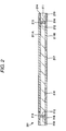
Figs. 2 to 7 are diagrams showing manufacturing steps of the related-art electronic apparatus. InFigs. 2 to 7 , the same numerals are assigned to the same components as those of the related-artelectronic apparatus 200. - First, in a step shown in
Fig. 2 , awiring substrate 201 is manufactured by a well-known technique. Next, in a step shown inFig. 3 , a plurality ofsemiconductor chips 202 to 204 are prepared. The plurality ofsemiconductor chips 202 to 204 are a semiconductor chip which is not a KGD (Known Good Die). - Then, in a step shown in
Fig. 4 ,sticky layers 232 are stuck on lower surfaces ofsemiconductor substrates semiconductor chips 202 to 204. Then, in a step shown inFig. 5 , thesemiconductor chips 202 to 204 on which thesticky layers 232 are formed are sequentially stacked on thewiring substrate 201 and thereafter, wire bonding connection between thewiring substrate 201 and thesemiconductor chips 202 to 204 is made usingmetal wires 222 to 224. - Then, in a step shown in
Fig. 6 , thesemiconductor chips 202 to 204 and themetal wires 222 to 224 are sealed with a sealing resin 205 (for example, a molding resin). Concretely, for example, thesealing resin 205 in a partially cured state is formed while applying a high pressure (for example, 5 MPa to 10 MPa) using a metal mold and thereafter, the sealingresin 205 in the partially cured state is heated (for example, 180 °C) and thesealing resin 205 is cured. - Then, in a step shown in
Fig. 7 , external connection terminals 206 (for example, solder bumps) are formed onpads 216 of thewiring substrate 201. Consequently, theelectronic apparatus 200 is manufactured (for example, see Patent Reference 1). [Patent Reference 1] Japanese Patent Unexamined Application Publication No.2007-5800 - However, in the related-art
electronic apparatus 200, thesemiconductor chips 202 to 204 which are not a KGD (Known Good Die) are stacked on thewiring substrate 201, so that there was a problem that a yield of theelectronic apparatus 200 reduces. - Also, by stacking the
semiconductor chips 202 to 204 on thewiring substrate 201 and thereafter forming the sealingresin 205 in a partially cured state while applying a high pressure (for example, 5 MPa to 10 MPa) using a metal mold and thereafter heating (for example, 180 °C) the sealingresin 205 in the partially cured state, the sealingresin 205 was cured and packaging processing was performed. As a result of that, due to influence of a highpressure or a high temperature, etc. in a step of formation of the sealingresin 205, thesemiconductor chips 202 to 204 are broken and a yield of theelectronic apparatus 200 reduces. - In light of the above, an electronic apparatus according to
independent claim 1 and a manufacturing method of an electronic apparatus according to independent claim 8 are provided.
Further advantages, features, aspects and details are evident from the dependent claims, the description and the drawings.
Exemplary embodiments of the present invention provide an electronic apparatus capable of improving a yield of the electronic apparatus by stacking semiconductor chips on a wiring substrate after previously performing WLP (Wafer Level Package) packaging processing of each of the semiconductor chips and forming a KGD before a sealing resin formation step, and a manufacturing method of the electronic apparatus. - According to one standpoint of the invention, there is provided an electronic apparatus comprising:
- a plurality of semiconductor apparatuses, each of semiconductor apparatuses having a semiconductor chip having an electrode pad, an internal connection terminal disposed on the electrode pad, a resin layer which is disposed on a surface of the semiconductor chip in which the electrode pad is formed and expose the internal connection terminal, and a wiring pattern which is disposed on the resin layer and is connected to the internal connection terminal;
- a wiring substrate on which the plurality of semiconductor apparatuses are stacked, the wiring substrate electrically connected to the plurality of semiconductor apparatuses through the wiring patterns; and
- a sealing resin with which the plurality of semiconductor apparatuses stacked on the wiring substrate are sealed,
- According to the invention, a plurality of semiconductor apparatuses (KGD (Known Good Die)) judged as good items in electrical and functional inspections made before being stacked on a wiring substrate while having resin layers which are disposed surfaces of semiconductor chips in which electrode pads are formed and expose the internal connection terminals and wiring patterns which are disposed on the resin layers and are connected to the internal connection terminals are stacked on the wiring substrate and thereby, a yield of an electronic apparatus can be improved.
- Also, since a high pressure or a high temperature, etc. at the time of forming the wiring pattern and the resin layer is applied to the semiconductor chips disposed in the plurality of semiconductor apparatuses judged as the good items before a sealing resin is formed. Consequently, the semiconductor chips disposed in the plurality of semiconductor apparatuses become resistant to breakage by influence of a pressure or a temperature, etc. at the time of forming the sealing resin (influence by a packaging processing process), so that a yield of the electronic apparatus can be improved.
- According to another standpoint of the invention, there is provided a manufacturing method of an electronic apparatus comprising a plurality of semiconductor apparatuses, a wiring substrate on which the plurality of semiconductor apparatuses are stacked, and a sealing resin with which the plurality of semiconductor apparatuses stacked on the wiring substrate are sealed, the method comprising:
- a semiconductor apparatus formation step of forming the plurality of semiconductor apparatuses;
- a good item semiconductor apparatus acquisition step of making electrical and functional inspections of the plurality of semiconductor apparatuses and acquiring a plurality of semiconductor apparatuses judged as good items;
- a semiconductor apparatus stacking step of stacking the plurality of semiconductor apparatuses judged as the good items on the wiring substrate;
- an electrical connection step of making electrical connection between the wiring substrate and the plurality of semiconductor apparatuses judged as the good items after the semiconductor apparatus stacking step; and
- a sealing resin formation step of sealing the plurality of semiconductor apparatuses judged as the good items with the sealing resin after the electrical connection step.
- According to the invention, electrical and functional inspections of a plurality of semiconductor apparatuses having resin layers which are disposed on surfaces of semiconductor chips in which electrode pads are formed and expose internal connection terminals and wiring patterns which are disposed on the resin layers and are connected to the internal connection terminals are made and the plurality of semiconductor apparatuses judged as good items are acquired and the plurality of semiconductor apparatuses (KGD (Known Good Die)) judged as the good items are stacked on the wiring substrate and then electrical connection between the wiring substrate and the stacked a plurality of semiconductor apparatuses are made and thereafter the plurality of semiconductor apparatuses are sealed with a sealing resin and thereby, a yield of an electronic apparatus can be improved.
- Also, since a high pressure or a high temperature, etc. at the time of forming the wiring pattern and the resin layer is applied to the semiconductor chips disposed in the plurality of semiconductor apparatuses judged as the good items before the sealing resin is formed. Consequently, the semiconductor chips disposed in the plurality of semiconductor apparatuses become resistant to breakage by influence of a pressure or a temperature, etc. at the time of forming the sealing resin (influence by a packaging processing process), so that a yield of the electronic apparatus can be improved.
- According to the invention, a yield of an electronic apparatus can be improved by preventing breakage of a semiconductor chip in a packaging processing process including a sealing resin formation step.
According to an embodiment, there are provided a plurality of semiconductor apparatuses judged as good items in electrical and functional inspections while having internal connection terminals disposed on electrode pads of semiconductor chips, resin layers which are disposed on surfaces of the semiconductor chips in which the electrode pads are formed and expose the internal connection terminals, and wiring patterns which are disposed on the resin layers and are connected to the internal connection terminals, a wiring substrate on which the plurality of semiconductor apparatuses are stepwise stacked, the wiring substrate electrically connected to the plurality of semiconductor apparatuses, and a sealing resin with which the plurality of semiconductor apparatuses are sealed.
Embodiments are also directed to apparatuses for carrying out the disclosed methods and including apparatus parts for performing described method steps. Furthermore, embodiments are also directed to methods by which the described apparatus operates or by which the described apparatus is manufactured. It may include method steps for carrying out functions of the apparatus or manufacturing parts of the apparatus. The method steps may be performed by way of hardware components, firmware, software, a computer programmed by appropriate software, by any combination thereof or in any other manner.
Other features and advantages maybe apparent from the following detailed description, the accompanying drawings and the claims. - So that the manner in which the above recited features of the present invention can be understood in detail, a more particular description of the invention, briefly summarized above, may be had by reference to embodiments. The accompanying drawings relate to embodiments of the invention and are described in the following:
-
Fig. 1 is a sectional diagram of a related-art electronic apparatus. -
Fig. 2 is a diagram showing a manufacturing step of the related-art electronic apparatus (first). -
Fig. 3 is a diagram showing a manufacturing step of the related-art electronic apparatus (second). -
Fig. 4 is a diagram showing a manufacturing step of the related-art electronic apparatus (third). -
Fig. 5 is a diagram showing a manufacturing step of the related-art electronic apparatus (fourth). -
Fig. 6 is a diagram showing a manufacturing step of the related-art electronic apparatus (fifth). -
Fig. 7 is a diagram showing a manufacturing step of the related-art electronic apparatus (sixth). -
Fig. 8 is a sectional diagram of an electronic apparatus according to an embodiment of the invention. -
Fig. 9 is a diagram showing a manufacturing step of the electronic apparatus according to the embodiment of the invention (first). -
Fig. 10 is a diagram showing a manufacturing step of the electronic apparatus according to the embodiment of the invention (second). -
Fig. 11 is a diagram showing a manufacturing step of the electronic apparatus according to the embodiment of the invention (third). -
Fig. 12 is a diagram showing a manufacturing step of the electronic apparatus according to the embodiment of the invention (fourth). -
Fig. 13 is a diagram showing a manufacturing step of the electronic apparatus according to the embodiment of the invention (fifth). -
Fig. 14 is a diagram showing a manufacturing step of the electronic apparatus according to the embodiment of the invention (sixth). -
Fig. 15 is a diagram showing a manufacturing step of the electronic apparatus according to the embodiment of the invention (seventh). -
Fig. 16 is a diagram showing a manufacturing step of the electronic apparatus according to the embodiment of the invention (eighth). -
Fig. 17 is a diagram showing a manufacturing step of the electronic apparatus according to the embodiment of the invention (ninth). -
Fig. 18 is a diagram showing a manufacturing step of the electronic apparatus according to the embodiment of the invention (tenth). -
Fig. 19 is a diagram showing a manufacturing step of the electronic apparatus according to the embodiment of the invention (eleventh). -
Fig. 20 is a diagram showing a manufacturing step of the electronic apparatus according to the embodiment of the invention (twelfth). -
Fig. 21 is a diagram showing a manufacturing step of the electronic apparatus according to the embodiment of the invention (thirteenth). -
Fig. 22 is a diagram showing a manufacturing step of the electronic apparatus according to the embodiment of the invention (fourteenth). -
Fig. 23 is a diagram showing a manufacturing step of the electronic apparatus according to the embodiment of the invention (fifteenth). -
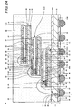
Fig. 24 is a diagram showing a manufacturing step of the electronic apparatus according to the embodiment of the invention (sixteenth). - Next, an embodiment of the invention will be described based on the drawings.
-
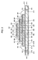
Fig. 8 is a sectional diagram of an electronic apparatus according to an embodiment of the invention. - Referring to
Fig. 8 , anelectronic apparatus 10 of the present embodiment has awiring substrate 11, semiconductor apparatuses 12-1 to 12-3 which are a plurality of semiconductor apparatuses, a sealingresin 13 andexternal connection terminals 14. - The
wiring substrate 11 has acore substrate 21, a through via 22, apad 23, solder resists 24, 28, a diffusionpreventive film 25 andpads 27 for external connection. Thecore substrate 21 is a substrate formed in a plate shape and has a throughhole 29. As a material of thecore substrate 21, for example, a glass epoxy resin or an FR-4 can be used. The through via 22 is disposed in the throughhole 29. The upper end of the through via 22 is connected to thepad 23 and the lower end of the through via 22 is connected to thepad 27 for external connection. The through via 22 is a via for making electrical connection between thepad 23 and thepad 27 for external connection. - The
pad 23 is disposed on an upper surface of the through via 22 and anupper surface 21A of thecore substrate 21. Thepad 23 is connected to the through via 22 and also is electrically connected to the semiconductor apparatus 12-1 through ametal wire 16 and the diffusionpreventive film 25. - The solder resist 24 is disposed so as to cover the
upper surface 21A of thecore substrate 21. The solder resist 24 has an opening part for exposing an upper surface of thepad 23. - The diffusion
preventive film 25 is disposed so as to cover the upper surface of thepad 23. The diffusionpreventive film 25 is connected to themetal wire 16 electrically connected to the semiconductor apparatus 12-1. As the diffusionpreventive film 25, for example, an Ni/Au film in which an Ni layer and an Au layer are sequentially provided on thepad 23 can be used. - The
pad 27 for external connection is disposed on a lower surface of the through via 22 and alower surface 21B of thecore substrate 21. Consequently, thepad 27 for external connection is connected to the through via 22. - The solder resist 28 is disposed so as to cover the
lower surface 21B of thecore substrate 21. The solder resist 28 has an opening part for exposing a lower surface of thepad 27 for external connection. - The semiconductor apparatus 12-1 has a
semiconductor chip 31, aninternal connection terminal 32, aresin layer 33, awiring pattern 35,dummy patterns 36, a solder resist 37 and a diffusionpreventive film 38. - The
semiconductor chip 31 has asemiconductor substrate 41, a semiconductor integratedcircuit 42, anelectrode pad 43 and aprotective film 44. Thesemiconductor substrate 41 is a substrate formed in a plate shape. As thesemiconductor substrate 41, for example, a silicon substrate can be used. In the case of using the silicon substrate as thesemiconductor substrate 41, a thickness of thesemiconductor substrate 41 can be set at, for example, 50 µm to 100 µm. - The semiconductor integrated
circuit 42 is disposed on the side of anupper surface 41A of thesemiconductor substrate 41. The semiconductor integratedcircuit 42 is a circuit constructed by a diffusion layer, an insulating film, a via and wiring (not shown). - The
electrode pad 43 is disposed on the semiconductor integratedcircuit 42. Theelectrode pad 43 is electrically connected to the diffusion layer, the via and the wiring (all are not shown) disposed in the semiconductor integratedcircuit 42. - The
protective film 44 is disposed on the semiconductor integratedcircuit 42 so as to expose theelectrode pad 43.protective film 44 is a film for protecting the semiconductor integratedcircuit 42. As theprotective film 44, for example, an SiN film or a PSG film can be used. Also, a polyimide film may be formed on a film such as the SiN film or the PSG film. - The
internal connection terminal 32 is disposedon the electrode pad43. Theinternal connection terminal 32 is electrically connected to the semiconductor integratedcircuit 42 through theelectrode pad 43. Anupper surface 32A of theinternal connection terminal 32 is formed in substantially a flat surface and is connected to thewiring pattern 35. A height of the internal connection terminal 32canbesetat, for example, 10 µm to 60 µm. As theinternal connection terminal 32, for example, an Au bump or a metal bump constructed of a Ni film formed by an electroless plating method and an Au film with which its Ni film is covered can be used. The Au bump can be formed by, for example, a bonding method or a plating method. - Substantially the flat
upper surface 32A of theinternal connection terminal 32 can be formed by, for example, pressing the upper ends of theinternal connection terminal 32 and theresin layer 33 by a flat plate to which a high pressure is applied after theresin layer 33 is formed so as to cover theinternal connection terminal 32. - The
resin layer 33 is disposed on theprotective film 44 so as to cover theupper surface 32A of theinternal connection terminal 32. Anupper surface 33A of theresin layer 33 is formed so as to be substantially flush with theupper surface 32A of theinternal connection terminal 32. As theresin layer 33, for example, a sheet-shaped resin having thermosetting properties (for example, an NCF (Non Conductive Film)), a pasty resin (for example, an NCP (Non Conductive Paste)) or an anisotropic conductive resin (for example, an ACF (Anisotropic Conductive Film)) can be used. A thickness of theresin layer 33 can be set at, for example, 10 µm to 60 µm. In the case of using the sheet-shaped resin having thermosetting properties, for example, 180 °C can be used as a heating temperature in the case of curing theresin layer 33. - The
wiring pattern 35 is disposed on theupper surface 32A of theinternal connection terminal 32 and theupper surface 33A of theresin layer 33. Consequently, thewiring pattern 35 is electrically connected to theinternal connection terminal 32. Thewiring pattern 35 has aconnection part 48 and apad 49 for inspection. Theconnection part 48 is electrically connected tometal wires preventive film 38. Thepad 49 for inspection is placed in a position spaced from theconnection part 48. Thepad 49 for inspection is a pad for test on which a probe pin disposed in a probe apparatus is abutted in the case of inspecting the semiconductor apparatus 12-1 using the probe apparatus (not shown) which is an inspection apparatus for making electrical and functional inspections. In addition, the functional inspection refers to an inspection such as an action check of the semiconductor integratedcircuit 42 disposed in the semiconductor chip 31 (for example, a check of the presence or absence of a reading error)). - By disposing the
pad 49 for inspection on which the probe pin of the probe apparatus is abutted in the case of making the electrical inspection of the semiconductor apparatus 12-1 in thewiring pattern 35 electrically connected to theinternal connection terminal 32 thus, the probe pin does not damage theconnection part 48, so that reliability of electrical connection between thewiring pattern 35 andmetal wires 16 to 18 can be improved. - As a material of the
wiring pattern 35 constructed above, for example, a Cu film can be used. In the case of using Cu as the material of thewiring pattern 35, a thickness of thewiring pattern 35 can be set at, for example, 5 µm to 15 µm, in particular 8 µm to 12µm. - The
dummy pattern 36 is disposed on theupper surface 33A of theresin layer 33 of the portion in which thewiring pattern 35 is not disposed. Thedummy pattern 36 is constructed so as to have the same material as that of thewiring pattern 35 and become substantially the same thickness as that of thewiring pattern 35. - By disposing the
dummy pattern 36 constructed by the same material as that of thewiring pattern 35 on theresin layer 33 of the portion in which thewiring pattern 35 is not disposed and setting a thickness of thedummy pattern 36 at substantially the same thickness as that of thewiring pattern 35 thus, warpage occurring in the semiconductor apparatus 12-1 can be reduced. Consequently, stacking the semiconductor apparatus 12-1 to thewiring substrate 11 is facilitated. - The solder resist 37 is disposed on the
upper surface 33A of theresin layer 33 so as to cover thedummy pattern 36 and thewiring pattern 35 of the portion excluding theconnection part 48 and thepad 49 for inspection. The solder resist 37 has an opening part for exposing an upper surface of theconnection part 48 and an opening part for exposing an upper surface of thepad 49 for inspection. - The diffusion
preventive film 38 is disposed on theconnection part 48 and thepad 49 for inspection. Themetal wire 16 electrically connected to thepad 23 of thewiring substrate 11 and themetal wire 17 electrically connected to the semiconductor apparatus 12-2 are connected to the diffusionpreventive film 38. Consequently, wire bonding connection to the semiconductor apparatus 12-2 and thewiring substrate 11 is made in the semiconductor apparatus 12-1. As the diffusionpreventive film 38, for example, an Ni/Au film in which an Ni layer and an Au layer are sequentially provided on theconnection part 48 and thepad 49 for inspection can be used. In the case of using the Ni/Au film as the diffusionpreventive film 38, a thickness of the Ni layer can be set at, for example, 2 µm to 5 µm, in particular 3µm to 4µm. In this case, a thickness of the Au layer can be set at, for example, 1 µm. - The semiconductor apparatus 12-1 constructed above is glued on the solder resist 24 of the
wiring substrate 11 by a sticky sheet 51 (concretely, for example, a die attach film) stuck on alower surface 41B of thesemiconductor substrate 41. The semiconductor apparatus 12-1 is a semiconductor apparatus (KGD (Known Good Die)) judged as a good item in electrical and functional inspections made before being glued on thewiring substrate 11. - The semiconductor apparatus 12-2 has a configuration similar to that of the semiconductor apparatus 12-1. The semiconductor apparatus 12-2 is glued on the solder resist 37 of the semiconductor apparatus 12-1 by a
sticky sheet 51 stuck on a lower surface of asemiconductor substrate 41. The semiconductor apparatus 12-2 is stepwise placed on the semiconductor apparatus 12-1 so as to expose the diffusionpreventive film 38 disposed on theconnection part 48 of the semiconductor apparatus 12-1. A diffusionpreventive film 38 disposed on aconnection part 48 of the semiconductor apparatus 12-2 is electrically connected to the semiconductor apparatuses 12-1, 12-3 through themetal wires - The semiconductor apparatus 12-2 constructed above is a semiconductor apparatus (KGD (Known Good Die)) judged as a good item in electrical and functional inspections made before being glued on the semiconductor apparatus 12-1.
- The semiconductor apparatus 12-3 has a configuration similar to that of the semiconductor apparatus 12-1. The semiconductor apparatus 12-3 is glued on a solder resist 37 of the semiconductor apparatus 12-2 by a
sticky sheet 51 stuck on a lower surface of asemiconductor substrate 41. The semiconductor apparatus 12-3 is stepwise placed on the semiconductor apparatus 12-2 so as to expose a diffusionpreventive film 38 disposed on aconnection part 48 of the semiconductor apparatus 12-2. A diffusionpreventive film 38 disposed on aconnection part 48 of the semiconductor apparatus 12-3 is electrically connected to the semiconductor apparatus 12-2 through themetal wire 18. That is, wire bonding connection between the semiconductor apparatus 12-3 and the semiconductor apparatus 12-2 is made. - The semiconductor apparatus 12-3 constructed above is a semiconductor apparatus (KGD (Known Good Die)) judged as a good item in electrical and functional inspections made before being glued on the semiconductor apparatus 12-2. The semiconductor apparatuses 12-1 to 12-3 are stepwise stacked.
- By stepwise stacking the semiconductor apparatuses 12-1 to 12-3 previously judged as the good items on the
wiring substrate 11 while having the resin layers 33 which are disposed on surfaces of the semiconductor chips 31 in which theelectrode pads 43 are formed and expose theinternal connection terminals 32 placed on theelectrode pads 43 and thewiring patterns 35 which are disposed on the resin layers 33 and are connected to theinternal connection terminals 32 thus, a yield of theelectronic apparatus 10 can be improved. - Also, since a load by packaging processing of a high pressure or a high temperature, etc. at the time of forming the
wiring pattern 35 and theresin layer 33 is applied to the semiconductor chips 31 disposed in the plurality of semiconductor apparatuses 12-1 to 12-3 previously judged as the good items before the sealingresin 13 is formed, the semiconductor chips 31 disposed in the plurality of semiconductor apparatuses 12-1 to 12-3 judged as the good items become resistant to breakage, so that a yield of theelectronic apparatus 10 can be improved. - The sealing
resin 13 is disposed on thewiring substrate 11 so as to seal themetal wires 16 to 18 and the semiconductor apparatuses 12-1 to 12-3 stacked. As the sealingresin 13, for example, a molding resin (for example, an epoxy resin) having thermosetting properties can be used. - The
external connection terminal 14 is arranged on thepad 27 for external connection of thewiring substrate 11. Theexternal connection terminal 14 is a terminal electrically connected to a mounting substrate (not shown) such as a motherboard. As theexternal connection terminal 14, for example, a solder bump can be used. - According to the electronic apparatus of the embodiment, by stepwise stacking the semiconductor apparatuses 12-1 to 12-3 (KGD (Known Good Die)) previously judged as the good items on the
wiring substrate 11 while having the resin layers 33 which are disposed on surfaces of the semiconductor chips 31 in which theelectrode pads 43 are formed and expose theinternal connection terminals 32 placed on theelectrode pads 43 and thewiring patterns 35 which are disposed on the resin layers 33 and are connected to theinternal connection terminals 32, a yield of theelectronic apparatus 10 can be improved. - Also, since a load by packaging processing of a high pressure or a high temperature, etc. at the time of forming the
wiring pattern 35 and theresin layer 33 is applied to the semiconductor chips 31 disposed in the plurality of semiconductor apparatuses 12-1 to 12-3 previously judged as the good items before the sealingresin 13 is formed, the semiconductor chips 31 disposed in the plurality of semiconductor apparatuses 12-1 to 12-3 previously judged as the good items become resistant to breakage by influence of a pressure or a temperature, etc. at the time of forming the sealingresin 13, so that a yield of theelectronic apparatus 10 can be improved. -
Figs. 9 to 24 are diagrams showing manufacturing steps of the electronic apparatus according to the embodiment of the invention. InFigs. 9 to 24 , the same numerals are assigned to the same components as those of theelectronic apparatus 10 of the embodiment. Also, inFigs. 9 to 17 , B shows a position (hereinafter called a "cut position B") in which a dicer or a slicer cuts asemiconductor substrate 61. - First, in a step shown in
Fig. 9 , thesemiconductor substrate 61 having a plurality of semiconductor apparatus formation regions A is prepared, and asemiconductor chip 31 having a semiconductor integratedcircuit 42, anelectrode pad 43 and aprotective film 44 is formed on the side of anupper surface 61A of thesemiconductor substrate 61 corresponding to the semiconductor apparatus formation region A by a well-known technique. The semiconductor apparatus formation region A is a region in which asemiconductor apparatus 12 is formed. Thesemiconductor apparatus 12 is a semiconductor apparatus having a configuration similar to that of the semiconductor apparatuses 12-1 to 12-3 (seeFig. 8 ) described above. Thesemiconductor substrate 61 results in the semiconductor substrate 41 (seeFig. 8 ) described above by being formed in a thin plate and being cut in the cut positions B in steps described below. - As the
semiconductor substrate 61, for example, a silicon wafer can be used. A thickness of thesemiconductor substrate 61 can be set at, for example, 500 µm to 775 µm, in particular 550µm to 650µm. As a material of theelectrode pad 43, for example, A1 can be used. Also, as theprotective film 44, for example, an SiN film or a PSG film can be used. - Next, in a step shown in
Fig. 10 , oneinternal connection terminal 32 is respectively formed on all theelectrode pads 43. As theinternal connection terminal 32, for example, an Au bump or a metal bump constructed of a Ni film formed by an electroless plating method and an Au film with which its Ni film is covered can be used. TheAubumpcanbeformedby, for example, abondingmethod. Inaddition, variations in height may be present in the plurality ofinternal connection terminals 32 formed in the step shown inFig. 10 . - Then, in a step shown in
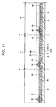
Fig. 11 , aresin layer 33 is formed so as to cover theinternal connection terminals 32 and the plurality of semiconductor chips 31 (the upper surface side of the plurality of semiconductor chips 31) of the side on which theinternal connection terminals 32 are disposed. As theresin layer 33, a sheet-shaped resin having thermosetting properties and sticky properties (for example, an NCF (Non Conductive Film)), a pasty resin having thermosetting properties (for example, an NCP (Non Conductive Paste)) or an anisotropic conductive resin (for example, an ACF (Anisotropic Conductive Film)) can be used. In the case of using the sheet-shaped resin having thermosetting properties and sticky properties, theresin layer 33 is formed by sticking the sheet-shaped resin on the upper surface side of a structural body shown inFig. 10 . Also, in the case of using the pasty resin as theresin layer 33, a pasty resin is formed on the upper surface side of the structural body shown inFig. 10 by a printing method etc. and thereafter is pre-baked and the resin is partially cured. This partially cured resin has adhesive properties. A thickness of theresin layer 33 can be set at, for example, 20 µm to 100 µm, in particular 40µm to 70µm. - Then, in a step shown in
Fig. 12 , ametal layer 63 is formed on anupper surface 33A of theresin layer 33. Themetal layer 63 is etched and results in awiring pattern 35 and adummy pattern 36 in a step shown inFig. 14 described below. Concretely, themetal layer 63 is formed on theupper surface 33A of theresin layer 33 by preparing Cu foil as themetal layer 63 and sticking this Cu foil on theupper surface 33A of theresin layer 33. A thickness of themetal layer 63 can be set at, for example, 5 µm to 15 µm, in particular 8µm to 12µm. - Then, in a step shown in
Fig. 13 , in a state of heating a structural body shown inFig. 12 (a heating temperature is, for example, 180 °C), a flat plate (not shown) is placed on themetal layer 63 and themetal layer 63 is pressed from the side of anupper surface 63A of themetal layer 63 through the flat plate (a pressure is, for example, 1.5 MPa to 3.0 MPa, in particular 2 Mpa) and alower surface 63B of themetal layer 63 is brought into contact withupper surfaces 32A of the plurality ofinternal connection terminals 32 and themetal layer 63 is crimped on theinternal connection terminals 32. Also, theresin layer 33 cures by heating the structural body shown inFig. 12 . A thickness of theresin layer 33 after crimping can be set at, for example, 10 µm to 60 µm, in particular 30 µm to 50µm. - Then, in a step shown in
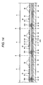
Fig. 14 , themetal layer 63 is patterned by etching andwiring patterns 35 anddummy patterns 36 are simultaneously formed and thereafter, roughening treatment of thewiring patterns 35 and thedummy patterns 36 is performed. Concretely, a resist film patterned is formed on themetal layer 63 and then using this resist film as a mask, themetal layer 63 is etched and thewiring patterns 35 and thedummy patterns 36 are formed. - By simultaneously forming the
wiring patterns 35 and thedummy patterns 36 thus, the manufacturing steps canbe simplified as compared with the case of separately forming thewiring patterns 35 and thedummy patterns 36. - The roughening treatment of the
wiring patterns 35 and thedummy patterns 36 can be performed by any method of blackening treatment or roughening etching treatment. The roughening treatment is treatment for improving adhesion between thewiring patterns 35 and thedummy patterns 36 and a solder resist 37 formed on side surfaces and upper surfaces of thewiring patterns 35 and thedummy patterns 36. - Then, in a step shown in
Fig. 15 , the solder resist 37 is disposed on theupper surface 33A of theresin layer 33 so as to cover thedummy patterns 36 and thewiring patterns 35 of the portion excludingconnection parts 48 andpads 49 for inspection and thereafter, a diffusionpreventive film 38 is formed on theconnection parts 48 and thepads 49 for inspection. The diffusionpreventive film 38 can be formed by, for example, a plating method. As the diffusionpreventive film 38, for example, an Ni/Au film in which an Ni layer and an Au layer are sequentially provided on theconnection parts 48 and thepads 49 for inspection can be used. In the case of using the Ni/Au film as the diffusionpreventive film 38, a thickness of the Ni layer can be set at, for example, 2 µm to 5 µm, in particular 3µm to 4µm. In this case, a thickness of the Au layer can be set at, for example, 1 µm. - Then, in a step shown in
Fig. 16 , thesemiconductor substrate 61 is polished or ground from the side of alower surface 61B of thesemiconductor substrate 61 and thesemiconductor substrate 61 is formed in a thin plate. In the thin plate formation of thesemiconductor substrate 61, for example, a back side grinder can be used. A thickness of thesemiconductor substrate 61 after the thin plate formation can be set at, for example, 50 µm to 100 µm, in particular 65µm to 85µm. - Then, in a step shown in
Fig. 17 , thesemiconductor substrate 61 formed in the thin plate is cut along the cut positions B. Consequently, a plurality ofsemiconductor apparatuses 12 are manufactured (the steps shown inFigs. 9 to 17 correspond to a semiconductor apparatus formation step). The plurality ofsemiconductor apparatuses 12 are semiconductor apparatuses having configurations similar to those of the semiconductor apparatuses 12-1 to 12-3 described above and also are the semiconductor apparatuses before electrical and functional inspections are made. In addition, the electrical and functional inspections of thesemiconductor apparatuses 12 may be made before thesemiconductor apparatuses 12 are individualized. - Then, in a step shown in
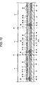
Fig. 18 , using a probe apparatus (not shown), a probe pin is brought into contact with the diffusionpreventive film 38 disposed on thepad 49 for inspection of thesemiconductor apparatus 12 shown inFig. 17 and the electrical and functional inspections of the plurality ofsemiconductor apparatuses 12 and the semiconductor apparatuses 12-1 to 12-3 (KGD (Known Good Die)) judged as good items are acquired (a good item semiconductor apparatus acquisition step). - Then, in a step shown in
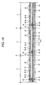
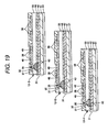
Fig. 19 ,sticky tapes 51 are stuck onlower surfaces 41B ofsemiconductor substrates 41 disposed in the semiconductor apparatuses 12-1 to 12-3 judged as the good items in the step shown inFig. 18 . As thesticky tape 51, for example, a die attach film can be used. Thesticky tape 51 may be stuck on thelower surface 41B of thesemiconductor substrate 41 disposed in thesemiconductor apparatus 12 before individualization. In this case, thesticky tape 51 is cut together with thesemiconductor substrate 61 formed in the thin plate. - Then, in a step shown in
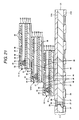
Fig. 20 , awiring substrate 11 is formed by a well-known technique. Then, in a step shown inFig. 21 , the semiconductor apparatuses 12-1 to 12-3 judged as the good items are sequentially stacked stepwise on thewiring substrate 11 shown inFig. 20 (a semiconductor apparatus stacking step). - At this time, the semiconductor apparatus 12-2 stepwise stacked on the semiconductor apparatus 12-1 is placed so as to expose the diffusion
preventive film 38 disposed on theconnection part 48 of the semiconductor apparatus 12-1, and the semiconductor apparatus 12-3 stepwise stacked on the semiconductor apparatus 12-2 is placed so as to expose the diffusionpreventive film 38 disposed on theconnection part 48 of the semiconductor apparatus 12-2. - Then, in a step shown in
Fig. 22 , electrical connection (wire bonding connection) between thewiring substrate 11 shown inFig. 21 and the semiconductor apparatuses 12-1 to 12-3 judged as the good items are made bymetal wires 16 to 18 (an electrical connection step). - Then, in a step shown in
Fig. 23 , a sealingresin 13 for sealing themetal wires 16 to 18 and the semiconductor apparatuses 12-1 to 12-3 judged as the good items shown inFig. 22 is formed (a sealing resin formation step). As the sealingresin 13, for example, a molding resin (for example, an epoxy resin) having thermosetting properties can be used. Concretely, in the case of using the molding resin having thermosetting properties as the sealingresin 13, a structural body shown inFig. 22 is received inside a metal mold and the molding resin to which a pressure (for example, 5 MPa to 10 MPa) is applied is introduced into the metal mold and thereafter the molding resin is heated (a heating temperature is, for example, 180 °C) and cured and thereby, the sealingresin 13 is formed. Since the high heat and the high pressure have already been applied to the semiconductor apparatuses 12-1 to 12-3 judged as the good items in the step shown inFig. 13 described above, the semiconductor chips 31 disposed in the semiconductor apparatuses 12-1 to 12-3 judged as the good items are not broken in a packaging processing process including the subsequent sealing resin formation step. - Then, in a step shown in
Fig. 24 ,external connection terminals 14 are formed onpads 27 for external connection of a structural body shown inFig. 23 . Consequently, anelectronic apparatus 10 of the embodiment is manufactured. As theexternal connection terminal 14, for example, a solder bump can be used. - According to the manufacturing method of the electronic apparatus of the embodiment, electrical and functional inspections of the plurality of
semiconductor apparatuses 12 having the resin layers 33 which are disposed on surfaces of the semiconductor chips 31 in which theelectrode pads 43 are formed and expose theinternal connection terminals 32 and thewiring patterns 35 which are disposed on the resin layers 33 and are connected to theinternal connection terminals 32 are made and the plurality of semiconductor apparatuses 12-1 to 12-3 (KGD (Known Good Die)) judged as good items are acquired and the semiconductor apparatuses 12-1 to 12-3 previously judged as the good items are stacked on thewiring substrate 11 and then electrical connection between thewiring substrate 11 and the stacked semiconductor apparatuses 12-1 to 12-3 are made and thereafter the semiconductor apparatuses 12-1 to 12-3 are sealed with the sealingresin 13 and thereby, a yield of theelectronic apparatus 10 can be improved. - Also, since a high pressure or a high temperature, etc. at the time of forming the
wiring pattern 35 and theresin layer 33 is applied to the semiconductor chips 31 disposed in the plurality of semiconductor apparatuses 12-1 to 12-3 previously judged as the good items before the sealingresin 13 is formed, the semiconductor chips 31 disposed in the plurality of semiconductor apparatuses 12-1 to 12-3 previously judged as the good items become resistant to breakage by influence of a pressure or a temperature, etc. at the time of forming the sealingresin 13, so that a yield of theelectronic apparatus 10 can be improved. - The preferred embodiment of the invention has been described above in detail, but the invention is not limited to such a specific embodiment and various modifications and changes can be made within the gist of the invention described in the claims. For example, in the embodiment, the case of stacking the semiconductor apparatuses 12-1 to 12-3 comprising the semiconductor chips 31 of the same kind on the
wiring substrate 11 has been described by way of example, but a plurality of semiconductor apparatuses comprising semiconductor chips of different kinds may be stacked on thewiring substrate 11 and may be sealed with the sealingresin 13. - Also, in the embodiment, the case of stacking three semiconductor apparatuses (semiconductor apparatuses 12-1 to 12-3) on the
wiring substrate 11 has been described by way of example, but the number of semiconductor apparatuses stacked on thewiring substrate 11 may be two or three or more. - Also, as shown in
Fig. 11 , in the case where the semiconductor apparatuses 12-1 to 12-3 in which the upper ends of theinternal connection terminals 32 are exposed and thereafter thewiring patterns 35 and thedummy patterns 36 are formed on the resin layers 33 are disposed in theelectronic apparatus 10, an effect similar to that of the embodiment can be obtained. That is, the manufacturing method of the semiconductor apparatuses 12-1 to 12-3 disposed in theelectronic apparatus 10 is not limited to the steps shown inFigs. 9 to 17 . - The invention can be applied to an electronic apparatus comprising a plurality of semiconductor chips (KGD (Known Good Die)) stacked on a wiring substrate and a sealing resin with which the plurality of semiconductor chips (KGD (Known Good Die)) are sealed, and a manufacturing method of the electronic apparatus.
Claims (10)
- An electronic apparatus (10) comprising:a plurality of semiconductor apparatuses (12-1, 12-2, 12-3), each of semiconductor apparatuses having a semiconductor chip (31) having an electrode pad (43), an internal connection terminal (32) disposed on the electrode pad, a resin layer (33) which is disposed on a surface of the semiconductor chip in which the electrode pad is formed and expose the internal connection terminal, and a wiring pattern (35) which is disposed on the resin layer and is connected to the internal connection terminal;a wiring substrate (11) on which the plurality of semiconductor apparatuses are stacked, the wiring substrate electrically connected to the plurality of semiconductor apparatuses through the wiring patterns; anda sealing resin (13) with which the plurality of semiconductor apparatuses stacked on the wiring substrate are sealed,wherein the plurality of semiconductor apparatuses are semiconductor apparatuses judged as good items in electrical and functional inspections made before being stacked on the wiring substrate.
- An electronic apparatus as claimed in claim 1, wherein the wiring pattern has a connection part to which a metal wire is connected, and the plurality of semiconductor apparatuses and the wiring substrate are connected to each other through wire bonding.
- An electronic apparatus as claimed in claim 2, wherein the plurality of semiconductor apparatuses (12-1, 12-2, 12-3) are stacked so as to expose the connection parts of the other semiconductor apparatuses.
- An electronic apparatus as claimed in claim 2 or 3, wherein a diffusion preventive film (25, 38) is disposed on the connection part, and the metal wire is connected to the diffusion preventive film.
- An electronic apparatus as in any one of claims 1 to 4, wherein the wiring pattern has an inspection pad for making the electrical and functional inspections of the semiconductor apparatus.
- An electronic apparatus as in any one of claims 1 to 5, wherein each of the plurality of semiconductor apparatuses has a dummy pattern made by the same material as that of the wiring pattern, the dummy pattern being disposed on the resin layer of a portion in which the wiring pattern is not disposed, the dummy pattern having a thickness set at substantially the same thickness as that of the wiring pattern.
- An electronic apparatus as in any one of claims 1 to 6, wherein the plurality of semiconductor apparatuses are stepwise stacked on the wiring substrate.
- A manufacturing method of an electronic apparatus comprising a plurality of semiconductor apparatuses, a wiring substrate on which the plurality of semiconductor apparatuses are stacked, and a sealing resin with which the plurality of semiconductor apparatuses stacked on the wiring substrate are sealed, comprising:a semiconductor apparatus formation step of forming the plurality of semiconductor apparatuses;a good item semiconductor apparatus acquisition step of making electrical and functional inspections of the plurality of semiconductor apparatuses and acquiring a plurality of semiconductor apparatuses judged as good items;a semiconductor apparatus stacking step of stacking the plurality of semiconductor apparatuses judged as the good items on the wiring substrate;an electrical connection step of making electrical connection between the wiring substrate and the plurality of semiconductor apparatuses judged as the good items after the semiconductor apparatus stacking step; anda sealing resin formation step of sealing the plurality of semiconductor apparatuses judged as the good items with the sealing resin after the electrical connection step.
- A manufacturing method of an electronic apparatus as claimed in claim 8, wherein the semiconductor apparatus formation step includes preparing semiconductor chips having electrode pads, forming internal connection terminals on the electrode pads, forming resin layers on surfaces of the semiconductor chips in which the electrode pads are formed so as to expose the internal connection terminals, and forming wiring patterns on the resin layers and connecting the wiring patterns to the internal connection terminals.
- A manufacturing method of an electronic apparatus as claimed in claim 8 or 9, wherein in the semiconductor apparatus staking step, the plurality of semiconductor apparatuses are stepwise stacked on the wiring substrate.
Applications Claiming Priority (1)
| Application Number | Priority Date | Filing Date | Title |
|---|---|---|---|
| JP2007250804A JP4317245B2 (en) | 2007-09-27 | 2007-09-27 | Electronic device and manufacturing method thereof |
Publications (2)
| Publication Number | Publication Date |
|---|---|
| EP2043152A2 true EP2043152A2 (en) | 2009-04-01 |
| EP2043152A3 EP2043152A3 (en) | 2010-03-17 |
Family
ID=40213481
Family Applications (1)
| Application Number | Title | Priority Date | Filing Date |
|---|---|---|---|
| EP08165316A Withdrawn EP2043152A3 (en) | 2007-09-27 | 2008-09-26 | Electronic apparatus with stacked semiconductor chips and manufacturing method thereof |
Country Status (6)
| Country | Link |
|---|---|
| US (2) | US20090085222A1 (en) |
| EP (1) | EP2043152A3 (en) |
| JP (1) | JP4317245B2 (en) |
| KR (1) | KR20090033012A (en) |
| CN (1) | CN101399256A (en) |
| TW (1) | TW200915533A (en) |
Cited By (1)
| Publication number | Priority date | Publication date | Assignee | Title |
|---|---|---|---|---|
| US9589930B2 (en) | 2014-01-16 | 2017-03-07 | Samsung Electronics Co., Ltd. | Semiconductor package including stepwise stacked chips |
Families Citing this family (36)
| Publication number | Priority date | Publication date | Assignee | Title |
|---|---|---|---|---|
| US9889043B2 (en) * | 2006-01-20 | 2018-02-13 | Lensar, Inc. | System and apparatus for delivering a laser beam to the lens of an eye |
| US7936057B2 (en) * | 2008-11-04 | 2011-05-03 | Seagate Technology Llc | High bandwidth package |
| WO2010073800A1 (en) * | 2008-12-22 | 2010-07-01 | 富士通株式会社 | Electronic component and method for manufacturing same |
| KR101026488B1 (en) * | 2009-08-10 | 2011-04-01 | 주식회사 하이닉스반도체 | Semiconductor package |
| KR101676620B1 (en) * | 2010-02-05 | 2016-11-16 | 에스케이하이닉스 주식회사 | Stacked semiconductor package |
| US8373280B2 (en) * | 2010-09-01 | 2013-02-12 | Oracle America, Inc. | Manufacturing fixture for a ramp-stack chip package using solder for coupling a ramp component |
| KR101061531B1 (en) * | 2010-12-17 | 2011-09-01 | 테세라 리써치 엘엘씨 | Enhanced stacked microelectronic assemblies with central contacts and improved ground or power distribution |
| WO2013153742A1 (en) * | 2012-04-11 | 2013-10-17 | パナソニック株式会社 | Semiconductor device |
| US9082632B2 (en) | 2012-05-10 | 2015-07-14 | Oracle International Corporation | Ramp-stack chip package with variable chip spacing |
| US8975754B2 (en) * | 2013-02-11 | 2015-03-10 | Oracle International Corporation | Chip package for high-count chip stacks |
| TWI616979B (en) * | 2014-03-14 | 2018-03-01 | Toshiba Memory Corporation | Semiconductor device and manufacturing method thereof |
| KR102161793B1 (en) * | 2014-07-18 | 2020-10-06 | 삼성전자주식회사 | Semiconductor devices and methods of manufacturing the same |
| TWI594341B (en) | 2015-01-19 | 2017-08-01 | 神盾股份有限公司 | Fingerprint identification device package and method of manufacturing same |
| JP2016192447A (en) | 2015-03-30 | 2016-11-10 | 株式会社東芝 | Semiconductor device |
| KR20170061816A (en) * | 2015-11-26 | 2017-06-07 | 에스케이하이닉스 주식회사 | Semiconductor package including molded stack die with terrace like edge |
| JP2017204511A (en) * | 2016-05-10 | 2017-11-16 | ソニー株式会社 | SEMICONDUCTOR DEVICE, SEMICONDUCTOR DEVICE MANUFACTURING METHOD, AND ELECTRONIC DEVICE |
| CN107579061B (en) | 2016-07-04 | 2020-01-07 | 晟碟信息科技(上海)有限公司 | Semiconductor device including interconnected stacked package |
| US9991235B2 (en) * | 2016-07-22 | 2018-06-05 | Invensas Corporation | Package on-package devices with upper RDL of WLPS and methods therefor |
| US10269706B2 (en) * | 2016-07-26 | 2019-04-23 | Taiwan Semiconductor Manufacturing Co., Ltd. | Semiconductor device and manufacturing method thereof |
| CN107768319B (en) * | 2016-08-18 | 2020-03-17 | 福州瑞芯微电子股份有限公司 | Packaging structure and method without electrical connection chip |
| CN107768259B (en) * | 2016-08-18 | 2020-04-24 | 福州瑞芯微电子股份有限公司 | Double-sided packaging structure and packaging method of chip |
| TWI668821B (en) * | 2016-10-25 | 2019-08-11 | Tdk Corporation | Electronic component module and manufacturing method thereof |
| CN109950223B (en) * | 2017-12-20 | 2021-01-26 | 晟碟半导体(上海)有限公司 | Semiconductor device including dual pad wirebond interconnect |
| CN107016158B (en) * | 2017-02-27 | 2020-04-17 | 中车大连机车车辆有限公司 | Method for inspecting electric wiring of urban rail vehicle |
| US10368448B2 (en) | 2017-11-11 | 2019-07-30 | At&S Austria Technologie & Systemtechnik Aktiengesellschaft | Method of manufacturing a component carrier |
| US10847505B2 (en) | 2018-04-10 | 2020-11-24 | Taiwan Semiconductor Manufacturing Company, Ltd. | Multi-chip semiconductor package |
| US11587903B2 (en) * | 2018-04-23 | 2023-02-21 | Advanced Semiconductor Engineering, Inc. | Semiconductor device package and a method of manufacturing the same |
| CN110660809B (en) * | 2018-06-28 | 2023-06-16 | 西部数据技术公司 | Semiconductor device including vertical interconnects for branched memory die modules |
| KR102534733B1 (en) * | 2018-07-31 | 2023-05-19 | 삼성전자 주식회사 | Fan-out semiconductor package having redistribution line structure |
| CN109192720B (en) | 2018-08-14 | 2020-10-30 | 苏州德林泰精工科技有限公司 | Stepped stacked chip packaging structure based on resin gasket and processing technology |
| JP7384820B2 (en) * | 2018-11-15 | 2023-11-21 | ローム株式会社 | semiconductor equipment |
| US10733136B1 (en) * | 2019-03-01 | 2020-08-04 | Western Digital Technologies, Inc. | Vertical surface mount type C USB connector |
| KR102798702B1 (en) * | 2019-07-22 | 2025-04-23 | 삼성전자주식회사 | Semiconductor package |
| JP7741745B2 (en) * | 2022-02-15 | 2025-09-18 | キオクシア株式会社 | Semiconductor device and manufacturing method thereof |
| JP2023121355A (en) * | 2022-02-21 | 2023-08-31 | キオクシア株式会社 | Semiconductor device and method for manufacturing semiconductor device |
| JP2024083816A (en) * | 2022-12-12 | 2024-06-24 | キオクシア株式会社 | Semiconductor device and method for manufacturing the same |
Citations (1)
| Publication number | Priority date | Publication date | Assignee | Title |
|---|---|---|---|---|
| JP2007005800A (en) | 2005-06-20 | 2007-01-11 | Stats Chippac Ltd | Module having stacked chip scale semiconductor package |
Family Cites Families (19)
| Publication number | Priority date | Publication date | Assignee | Title |
|---|---|---|---|---|
| JP2000243876A (en) * | 1999-02-23 | 2000-09-08 | Fujitsu Ltd | Semiconductor device and manufacturing method thereof |
| JP3756041B2 (en) * | 1999-05-27 | 2006-03-15 | Hoya株式会社 | Manufacturing method of multilayer printed wiring board |
| JP2001127256A (en) * | 1999-10-29 | 2001-05-11 | Fuji Xerox Co Ltd | Semiconductor device |
| JP3813788B2 (en) | 2000-04-14 | 2006-08-23 | 株式会社ルネサステクノロジ | Semiconductor device and manufacturing method thereof |
| US6921979B2 (en) * | 2002-03-13 | 2005-07-26 | Freescale Semiconductor, Inc. | Semiconductor device having a bond pad and method therefor |
| US6784544B1 (en) * | 2002-06-25 | 2004-08-31 | Micron Technology, Inc. | Semiconductor component having conductors with wire bondable metalization layers |
| JP2004140037A (en) * | 2002-10-15 | 2004-05-13 | Oki Electric Ind Co Ltd | Semiconductor device and manufacturing method thereof |
| US20040191955A1 (en) * | 2002-11-15 | 2004-09-30 | Rajeev Joshi | Wafer-level chip scale package and method for fabricating and using the same |
| JP3825753B2 (en) * | 2003-01-14 | 2006-09-27 | 株式会社東芝 | Manufacturing method of semiconductor device |
| US6861288B2 (en) * | 2003-01-23 | 2005-03-01 | St Assembly Test Services, Ltd. | Stacked semiconductor packages and method for the fabrication thereof |
| JP3880572B2 (en) * | 2003-10-31 | 2007-02-14 | 沖電気工業株式会社 | Semiconductor chip and semiconductor device |
| US7091124B2 (en) * | 2003-11-13 | 2006-08-15 | Micron Technology, Inc. | Methods for forming vias in microelectronic devices, and methods for packaging microelectronic devices |
| US7095105B2 (en) * | 2004-03-23 | 2006-08-22 | Texas Instruments Incorporated | Vertically stacked semiconductor device |
| JP2005302871A (en) | 2004-04-08 | 2005-10-27 | Toshiba Corp | Multilayer semiconductor device and manufacturing method thereof. |
| US8324725B2 (en) * | 2004-09-27 | 2012-12-04 | Formfactor, Inc. | Stacked die module |
| DE102004049356B4 (en) * | 2004-10-08 | 2006-06-29 | Infineon Technologies Ag | Semiconductor module with an internal semiconductor chip stack and method for producing the same |
| JP4972306B2 (en) * | 2004-12-21 | 2012-07-11 | オンセミコンダクター・トレーディング・リミテッド | Semiconductor device and circuit device |
| JP2006294650A (en) * | 2005-04-05 | 2006-10-26 | Oki Electric Ind Co Ltd | Electronic component mounting method |
| JP4287458B2 (en) * | 2005-11-16 | 2009-07-01 | サムソン エレクトロ−メカニックス カンパニーリミテッド. | Printed circuit board using paste bump and manufacturing method thereof |
-
2007
- 2007-09-27 JP JP2007250804A patent/JP4317245B2/en not_active Expired - Fee Related
-
2008
- 2008-09-22 KR KR1020080092491A patent/KR20090033012A/en not_active Withdrawn
- 2008-09-26 TW TW097137226A patent/TW200915533A/en unknown
- 2008-09-26 US US12/238,699 patent/US20090085222A1/en not_active Abandoned
- 2008-09-26 EP EP08165316A patent/EP2043152A3/en not_active Withdrawn
- 2008-09-27 CN CNA2008101488322A patent/CN101399256A/en active Pending
-
2009
- 2009-10-02 US US12/588,076 patent/US7875499B2/en active Active
Patent Citations (1)
| Publication number | Priority date | Publication date | Assignee | Title |
|---|---|---|---|---|
| JP2007005800A (en) | 2005-06-20 | 2007-01-11 | Stats Chippac Ltd | Module having stacked chip scale semiconductor package |
Cited By (2)
| Publication number | Priority date | Publication date | Assignee | Title |
|---|---|---|---|---|
| US9589930B2 (en) | 2014-01-16 | 2017-03-07 | Samsung Electronics Co., Ltd. | Semiconductor package including stepwise stacked chips |
| US10157883B2 (en) | 2014-01-16 | 2018-12-18 | Samsung Electronics Co., Ltd. | Semiconductor package including stepwise stacked chips |
Also Published As
| Publication number | Publication date |
|---|---|
| TW200915533A (en) | 2009-04-01 |
| US20100022035A1 (en) | 2010-01-28 |
| US7875499B2 (en) | 2011-01-25 |
| KR20090033012A (en) | 2009-04-01 |
| JP4317245B2 (en) | 2009-08-19 |
| EP2043152A3 (en) | 2010-03-17 |
| CN101399256A (en) | 2009-04-01 |
| JP2009081355A (en) | 2009-04-16 |
| US20090085222A1 (en) | 2009-04-02 |
Similar Documents
| Publication | Publication Date | Title |
|---|---|---|
| US7875499B2 (en) | Method of manufacturing a stacked semiconductor apparatus | |
| US7772091B2 (en) | Manufacturing method of semiconductor apparatus comprising alignment patterns in scribe regions | |
| US6706547B2 (en) | Method of manufacturing a circuit device with trenches in a conductive foil | |
| US5731709A (en) | Method for testing a ball grid array semiconductor device and a device for such testing | |
| US8344492B2 (en) | Semiconductor device and method of manufacturing the same, and electronic apparatus | |
| US20090291515A1 (en) | Semiconductor device and a semiconductor device manufacturing method | |
| KR100849181B1 (en) | Semiconductor package, method of manufacturing the same, and semiconductor package molding apparatus and molding method for manufacturing the same | |
| EP2141972A1 (en) | Component-incorporating module and its manufacturing method | |
| EP1906445A2 (en) | Manufacturing method of semiconductor device | |
| CN114256170B (en) | Fan-out packaging structure and preparation method thereof | |
| US7615408B2 (en) | Method of manufacturing semiconductor device | |
| JP5543084B2 (en) | Manufacturing method of semiconductor device | |
| US20150351234A1 (en) | Support structure for stacked integrated circuit dies | |
| US7964493B2 (en) | Method of manufacturing semiconductor device | |
| EP2071622A2 (en) | Package for semiconductor device and method of manufacturing the same | |
| CN101656246B (en) | Chip stack packaging structure with substrate with opening and packaging method thereof | |
| KR102320098B1 (en) | Electrical characteristic inspection method | |
| CN101656247A (en) | Semiconductor packaging structure | |
| US7100814B2 (en) | Method for preparing integrated circuit modules for attachment to printed circuit substrates | |
| CN100466209C (en) | Semiconductor device and processing and packaging method thereof | |
| US10504806B2 (en) | Semiconductor package with electrical test pads | |
| MX2008012339A (en) | Methods for attaching a flip chip integrated circuit assembly to a substrate. | |
| WO2019103676A1 (en) | Ultra-thin fingerprint sensor component and manufacturing method | |
| KR101690859B1 (en) | Manufacturing method of a semiconductor substrate and the package | |
| JP2002026188A (en) | Method of manufacturing ball grid array type semiconductor device |
Legal Events
| Date | Code | Title | Description |
|---|---|---|---|
| PUAI | Public reference made under article 153(3) epc to a published international application that has entered the european phase |
Free format text: ORIGINAL CODE: 0009012 |
|
| AK | Designated contracting states |
Kind code of ref document: A2 Designated state(s): AT BE BG CH CY CZ DE DK EE ES FI FR GB GR HR HU IE IS IT LI LT LU LV MC MT NL NO PL PT RO SE SI SK TR |
|
| AX | Request for extension of the european patent |
Extension state: AL BA MK RS |
|
| PUAL | Search report despatched |
Free format text: ORIGINAL CODE: 0009013 |
|
| AK | Designated contracting states |
Kind code of ref document: A3 Designated state(s): AT BE BG CH CY CZ DE DK EE ES FI FR GB GR HR HU IE IS IT LI LT LU LV MC MT NL NO PL PT RO SE SI SK TR |
|
| AX | Request for extension of the european patent |
Extension state: AL BA MK RS |
|
| RIC1 | Information provided on ipc code assigned before grant |
Ipc: H01L 23/58 20060101ALI20100210BHEP Ipc: H01L 23/31 20060101ALI20100210BHEP Ipc: H01L 25/065 20060101AFI20090126BHEP |
|
| AKY | No designation fees paid | ||
| STAA | Information on the status of an ep patent application or granted ep patent |
Free format text: STATUS: THE APPLICATION IS DEEMED TO BE WITHDRAWN |
|
| 18D | Application deemed to be withdrawn |
Effective date: 20100918 |
|
| REG | Reference to a national code |
Ref country code: DE Ref legal event code: R108 Effective date: 20110222 Ref country code: DE Ref legal event code: 8566 |